EP2290789A1 - Rectifier of ac generator for vehicle - Google Patents
Rectifier of ac generator for vehicle Download PDFInfo
- Publication number
- EP2290789A1 EP2290789A1 EP08765642A EP08765642A EP2290789A1 EP 2290789 A1 EP2290789 A1 EP 2290789A1 EP 08765642 A EP08765642 A EP 08765642A EP 08765642 A EP08765642 A EP 08765642A EP 2290789 A1 EP2290789 A1 EP 2290789A1
- Authority
- EP
- European Patent Office
- Prior art keywords
- bent
- rectifying device
- connection lead
- vehicle alternator
- chip
- Prior art date
- Legal status (The legal status is an assumption and is not a legal conclusion. Google has not performed a legal analysis and makes no representation as to the accuracy of the status listed.)
- Granted
Links
Images

Classifications
-
- H—ELECTRICITY
- H02—GENERATION; CONVERSION OR DISTRIBUTION OF ELECTRIC POWER
- H02K—DYNAMO-ELECTRIC MACHINES
- H02K11/00—Structural association of dynamo-electric machines with electric components or with devices for shielding, monitoring or protection
- H02K11/04—Structural association of dynamo-electric machines with electric components or with devices for shielding, monitoring or protection for rectification
- H02K11/049—Rectifiers associated with stationary parts, e.g. stator cores
- H02K11/05—Rectifiers associated with casings, enclosures or brackets
Definitions
- the present invention relates to a rectifying device of a vehicle alternator that is incorporated in the vehicle alternator and rectifies an AC output voltage of the vehicle alternator into a DC voltage.
- a conventional vehicle alternator has a field current fed to an exciting coil thereof via a brush and a slip ring.
- a rotating torque for an engine is conveyed to a rotation shaft by way of a pulley and a belt, and a rotor is driven to rotate.
- a rectifying device is attached to a rear bracket, is connected to an output terminal of a stator coil, and converts an AC output voltage, which is developed at the stator, into a DC voltage.
- a diode included in the rectifying device has an IC chip soldered to a copper base.
- a copper relay lead is soldered to the IC chip, and a copper connection lead is further soldered to the relay lead.
- the IC chip is then molded with a sealing resin body.
- Patent Document 1 Japanese Patent No. 3839576
- connection lead has a bend or a bent part so that a stress generated at an IC chip due to a vibration stemming from attachment to a vehicle can be alleviated.
- the bend or bent part causes concentration of the stress.
- the bend or bent part is located close to a junction region with respect to the IC chip or relay lead, a large stress is generated due to a displacement of the junction region by the vibration. This poses a problem in that the connection lead is broken at the bend or bent part.
- An object of the present invention is to provide a rectifying device of a vehicle alternator capable of improving the vibration resistance of a diode.
- the present invention is a rectifying device of a vehicle alternator that includes a heat sink, a circuit board which has a connection terminal disposed to be orthogonal to the heat sink and which is disposed in parallel with the heat sink, and a diode which includes a metallic base having one surface thereof joined to the heat sink, an IC chip joined to the other surface of the metallic base, a sealing resin body with which the IC chip is molded, and a connection lead having one end thereof electrically coupled to the IC chip and having the other end thereof joined to the connection terminal of the circuit board.
- the rectifying device is incorporated in the vehicle alternator, and rectifies an AC output voltage of the vehicle alternator into a DC voltage.
- connection lead of the diode has a linear part extended in parallel from the metallic base and bared from the sealing resin body, and a bent part that is bent 90° or more substantially like an arc from the linear part.
- the bending radius R of the bent part is set to a value larger than a separation distance w in a horizontal direction between the root of the linear part bared from the sealing resin body and the distal part of the connection lead.
- the bending radius R of the bent part of the connection lead of the diode can be made large, even if the rectifying device is downsized, concentration of a generated stress on the bent part of the connection lead of the diode can be alleviated and breakage of the bent part can be suppressed.
- the highly reliable rectifying device of the vehicle alternator can be provided.
- Fig. 1 is a sectional view showing a vehicle alternator in which a rectifying device in accordance with Embodiment 1 of the present invention is incorporated
- Fig. 2 is a perspective view showing the rectifying device shown in Fig. 1
- a stator 1 includes a stator core 2 and a stator coil 3 wound around the stator core 2.
- a rotor 4 includes a pair of pole cores 5 and 6 that are opposed to each other, an exciting coil 7 interposed between the cores 5 and 6, a rotation shaft 8, and a slip ring 9 fixed to the rotation shaft 8.
- a rear bracket 13 is fixed to a front bracket 12 by a fastening bolt 14, and the stator 1 is supported between the front bracket 12 and rear bracket 13.
- the rotation shaft 8 is borne by the front bracket 12 and rear bracket 13 via bearings 15 and 16-A pulley 17 is fixed to one end of the rotation shaft 8.
- a rectifying device 18 is attached to the rear bracket 13, is connected to an output terminal of the stator coil 3, and converts an AC voltage developed at the stator 1 into a DC voltage.
- a voltage regulator 19 is attached to the rear bracket 13 together with a brush holder 20.
- the brush holder 20 bears a brush 21 so that the brush 21 can abut against the slip ring 9.
- a field current is fed to the exciting coil 7 via the brush 21 and the slip ring 9.
- a rotating torque for an engine is conveyed to the rotation shaft 8 by way of the pulley 17 and a belt (not shown).
- the rotor 4 is driven to rotate.
- This causes the stator 1 to develop an AC voltage.
- the AC voltage is converted into a DC voltage by the rectifying device 18.
- the rectifying device 18 includes a + side heat sink 30 having plural + side diodes 33 mounted therein, a - side heat sink 31 having plural - side diodes 34 mounted therein, and a circuit board assembly 32.
- the + side heat sink 30 is made of aluminum and includes a notched annular part 30a and plural heat radiation fins 30b stood on the rear side of the notched annular part 30a.
- Positioning guides 30c are extended from three respective positions on the notched annular part, that is, at both the ends of the notched annular part 30a and in the center thereof to outside in a radial direction.
- Plural + side diode mounts 30d are formed convexly in a circumferential direction of the principal surface of the notched annular part 30a.
- the plural + side diodes 33 are joined to the respective + side diode mounts 30d, and thus mounted in the circumferential direction on the principal surface of the notched annular part 30a.
- the - side heat sink 31 is made of aluminum, and includes a notched annular part 31a, guide portions 31b disposed at three positions on the notched annular part 31a, that is, at both the ends of the notched annular part 31a and in the center thereof, and plural - side diode mounts 31c formed concavely in a circumferential direction in the principal surface of the notched annular part 31a.
- the plural - side diodes 34 are joined to the respective - side diode mounts 31c, and thus mounted in the circumferential direction on the principal surface of the notched annular part 31a.
- the circuit board 32 includes a resin body 36 that has an iron circuit board molded with a polyphenylene sulfide (PPS) and shaped like a notched annulus, and guide portions 36a formed at three positions on the resin body 36, that is, at both the ends of the resin body 36 and in the center thereof. Connection terminals 37 of the circuit board are jutted downward from the resin body 36 at plural positions in the circumferential direction.
- PPS polyphenylene sulfide
- Fig. 3 is a schematic side view of a diode adapted to the rectifying device in accordance with Embodiment 1.
- the + side diode 33 has an IC chip 33a soldered to a metallic base 33b made of copper, has a relay lead 33c, which is made of copper, soldered to the IC chip 33a, has a connection lead 33d, which is made of copper, soldered to the relay lead 33c, so as to be molded with a sealing resin body 33e.
- the connection lead 33d has a shape of being bent nearly at right angles while forming a bent part 33g that is bent 90° or more substantially like an arc from a linear part 33f extended from the sealing resin body 33e in parallel with the metallic base 33b.
- a junction region 33h to be joined to the connection terminal 37 of the circuit board is formed.
- the bending radius R of the bent part 33g of the connection lead 33d is set to a value larger than a separation distance w in a horizontal direction between the terminal of the linear part 33f and the distal part of the connection lead 33d.
- the - side diode 34 is constructed similarly to the + side diode 33.
- the bending radius R of the bent part 33g can be increased. Therefore, concentration of a generated stress on the bent part 33g can be alleviated, and breakage of the bent part 33g can be suppressed.
- the bent part 33g acts as a spring structure, a vibration can be absorbed, and a stress generated at the IC chip 3:3a can be reduced.
- Embodiment 1 when the bending radius R is larger, a stress generated at the bending part 33g is more greatly alleviated.
- 1 [mm] denotes the distance from the root of the connection lead 33d to the neutral line of a region bent at right angles
- h [mm] denotes the distance from the neutral line of the linear part 33f to the junction region 33h of the distal part of the connection lead
- it is under h>21 that the stress is alleviated owing to the formation of the bent part 33a.
- h ⁇ 21 it is better not to form the bent part 33g.
- a bent part 40 of a bending radius R' ⁇ 1 is merely formed as shown in Fig. 5 , the bend part 40 fills the role of a damper that absorbs a vibration stemming from attachment to a vehicle.
- the bending radius R' is small, a damper effect is limited. A stress generated at the IC chip 33a cannot be reduced.
- the bending radius R' is small, concentration of the generated stress on the bent part is intense. The connection lead is broken at the bent part.
- a bend 41 is formed in the linear part as shown in Fig.
- the bent part 33g like the one in Embodiment 1 shown in Fig. 3
- the bent part 33g acts as a spring structure
- concentration of the generated stress on the bent part can be alleviated.
- the distance between the junction region 33h and bent part 33g is large. Therefore, a stress generated due to a displacement of the junction region can be reduced. Eventually, the stress generated at the IC chip 33a can be reduced without breakage of the connection lead 33d.
- the present invention is not limited to the shape of the connection lead 33d shown in Fig. 3 . Even with, for example, a shape of being bent at right angles from the bent part 33g through an inclined part 33i as shown in Fig. 7 , the same advantage is exerted.
Landscapes
- Engineering & Computer Science (AREA)
- Power Engineering (AREA)
- Synchronous Machinery (AREA)
Abstract
Description
- The present invention relates to a rectifying device of a vehicle alternator that is incorporated in the vehicle alternator and rectifies an AC output voltage of the vehicle alternator into a DC voltage.
- As described in Patent Document 1, a conventional vehicle alternator has a field current fed to an exciting coil thereof via a brush and a slip ring. At the same time, a rotating torque for an engine is conveyed to a rotation shaft by way of a pulley and a belt, and a rotor is driven to rotate. This causes a stator to develop an AC voltage. A rectifying device is attached to a rear bracket, is connected to an output terminal of a stator coil, and converts an AC output voltage, which is developed at the stator, into a DC voltage.
A diode included in the rectifying device has an IC chip soldered to a copper base. A copper relay lead is soldered to the IC chip, and a copper connection lead is further soldered to the relay lead. The IC chip is then molded with a sealing resin body. - Patent Document 1: Japanese Patent No.
3839576 - In the foregoing rectifying device, the connection lead has a bend or a bent part so that a stress generated at an IC chip due to a vibration stemming from attachment to a vehicle can be alleviated. The bend or bent part causes concentration of the stress. In addition, since the bend or bent part is located close to a junction region with respect to the IC chip or relay lead, a large stress is generated due to a displacement of the junction region by the vibration. This poses a problem in that the connection lead is broken at the bend or bent part.
- The present invention is intended to solve the foregoing problem. An object of the present invention is to provide a rectifying device of a vehicle alternator capable of improving the vibration resistance of a diode.
- The present invention is a rectifying device of a vehicle alternator that includes a heat sink, a circuit board which has a connection terminal disposed to be orthogonal to the heat sink and which is disposed in parallel with the heat sink, and a diode which includes a metallic base having one surface thereof joined to the heat sink, an IC chip joined to the other surface of the metallic base, a sealing resin body with which the IC chip is molded, and a connection lead having one end thereof electrically coupled to the IC chip and having the other end thereof joined to the connection terminal of the circuit board. The rectifying device is incorporated in the vehicle alternator, and rectifies an AC output voltage of the vehicle alternator into a DC voltage. Herein, the connection lead of the diode has a linear part extended in parallel from the metallic base and bared from the sealing resin body, and a bent part that is bent 90° or more substantially like an arc from the linear part. The bending radius R of the bent part is set to a value larger than a separation distance w in a horizontal direction between the root of the linear part bared from the sealing resin body and the distal part of the connection lead.
- According to the present invention, since the bending radius R of the bent part of the connection lead of the diode can be made large, even if the rectifying device is downsized, concentration of a generated stress on the bent part of the connection lead of the diode can be alleviated and breakage of the bent part can be suppressed. The highly reliable rectifying device of the vehicle alternator can be provided.
-
-
Fig. 1 is a sectional view showing a vehicle alternator in which a rectifying device in accordance with Embodiment 1 of the present invention is incorporated; -
Fig. 2 is a perspective view showing the rectifying device in accordance with Embodiment 1; -
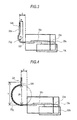
Fig. 3 is a schematic side view of a diode adapted to the rectifying device in accordance with Embodiment 1; -
Fig. 4 is a schematic explanatory diagram for explaining the shape of a lead of the diode in Embodiment 1; -
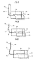
Fig. 5 is a schematic side view of a diode adapted to a conventional rectifying device; -
Fig. 6 is a schematic side view showing another example of the diode adapted to the conventional rectifying device; and -
Fig. 7 is a schematic side view showing another example of the diode adapted to the rectifying device in accordance with Embodiment 1. -
- 100:
- vehicle alternator
- 18:
- rectifying device
- 30:
- heat sink
- 32:
- circuit board
- 33:
- diode
- 33a:
- IC chip
- 33b:
- metallic base
- 33c:
- relay lead
- 33d:
- connection lead
- 33e:
- sealing resin body
- 33f:
- linear part
- 33g:
- bent part
- 33h:
- junction region
- 33i:
- inclined part
- 34:
- diode
- 37:
- connection terminal
-
Fig. 1 is a sectional view showing a vehicle alternator in which a rectifying device in accordance with Embodiment 1 of the present invention is incorporated, andFig. 2 is a perspective view showing the rectifying device shown inFig. 1 .
InFig. 1 , a stator 1 includes astator core 2 and astator coil 3 wound around thestator core 2. Arotor 4 includes a pair of pole cores 5 and 6 that are opposed to each other, an exciting coil 7 interposed between the cores 5 and 6, arotation shaft 8, and aslip ring 9 fixed to therotation shaft 8. Arear bracket 13 is fixed to afront bracket 12 by afastening bolt 14, and the stator 1 is supported between thefront bracket 12 andrear bracket 13. Therotation shaft 8 is borne by thefront bracket 12 andrear bracket 13 viabearings 15 and 16-A pulley 17 is fixed to one end of therotation shaft 8. A rectifyingdevice 18 is attached to therear bracket 13, is connected to an output terminal of thestator coil 3, and converts an AC voltage developed at the stator 1 into a DC voltage. Avoltage regulator 19 is attached to therear bracket 13 together with abrush holder 20. Thebrush holder 20 bears abrush 21 so that thebrush 21 can abut against theslip ring 9. - In the
vehicle alternator 100, a field current is fed to the exciting coil 7 via thebrush 21 and theslip ring 9. At the same time, a rotating torque for an engine is conveyed to therotation shaft 8 by way of thepulley 17 and a belt (not shown). Thus, therotor 4 is driven to rotate. This causes the stator 1 to develop an AC voltage. The AC voltage is converted into a DC voltage by the rectifyingdevice 18. - Now, referring to
Fig. 2 , the construction of the rectifyingdevice 18 will be described below.
The rectifyingdevice 18 includes a +side heat sink 30 having plural +side diodes 33 mounted therein, a -side heat sink 31 having plural -side diodes 34 mounted therein, and acircuit board assembly 32.
The +side heat sink 30 is made of aluminum and includes a notchedannular part 30a and pluralheat radiation fins 30b stood on the rear side of the notchedannular part 30a. Positioning guides 30c are extended from three respective positions on the notched annular part, that is, at both the ends of the notchedannular part 30a and in the center thereof to outside in a radial direction. Plural + side diode mounts 30d are formed convexly in a circumferential direction of the principal surface of the notchedannular part 30a. The plural +side diodes 33 are joined to the respective + side diode mounts 30d, and thus mounted in the circumferential direction on the principal surface of the notchedannular part 30a.
The -side heat sink 31 is made of aluminum, and includes a notchedannular part 31a, guide portions 31b disposed at three positions on the notchedannular part 31a, that is, at both the ends of the notchedannular part 31a and in the center thereof, and plural - side diode mounts 31c formed concavely in a circumferential direction in the principal surface of the notchedannular part 31a. The plural -side diodes 34 are joined to the respective - side diode mounts 31c, and thus mounted in the circumferential direction on the principal surface of the notchedannular part 31a.
Thecircuit board 32 includes aresin body 36 that has an iron circuit board molded with a polyphenylene sulfide (PPS) and shaped like a notched annulus, and guideportions 36a formed at three positions on theresin body 36, that is, at both the ends of theresin body 36 and in the center thereof.Connection terminals 37 of the circuit board are jutted downward from theresin body 36 at plural positions in the circumferential direction. -
Fig. 3 is a schematic side view of a diode adapted to the rectifying device in accordance with Embodiment 1.
InFig. 3 , the +side diode 33 has anIC chip 33a soldered to ametallic base 33b made of copper, has arelay lead 33c, which is made of copper, soldered to theIC chip 33a, has aconnection lead 33d, which is made of copper, soldered to therelay lead 33c, so as to be molded with a sealingresin body 33e.
Theconnection lead 33d has a shape of being bent nearly at right angles while forming abent part 33g that is bent 90° or more substantially like an arc from alinear part 33f extended from the sealingresin body 33e in parallel with themetallic base 33b. In the distal part thereof, ajunction region 33h to be joined to theconnection terminal 37 of the circuit board is formed.
Herein, the bending radius R of thebent part 33g of theconnection lead 33d is set to a value larger than a separation distance w in a horizontal direction between the terminal of thelinear part 33f and the distal part of theconnection lead 33d.
Incidentally, the -side diode 34 is constructed similarly to the +side diode 33. - Along with downsizing of the rectifying
device 18, even when the distance 1 between the junction region of theconnection lead 33d (part to be joined to theconnection terminal 37 of the circuit board 32) and the bared root of thelinear part 33f is short, the bending radius R of thebent part 33g can be increased. Therefore, concentration of a generated stress on thebent part 33g can be alleviated, and breakage of thebent part 33g can be suppressed.
In addition, since thebent part 33g acts as a spring structure, a vibration can be absorbed, and a stress generated at the IC chip 3:3a can be reduced. - In Embodiment 1, when the bending radius R is larger, a stress generated at the bending
part 33g is more greatly alleviated. Assuming that 1 [mm] denotes the distance from the root of theconnection lead 33d to the neutral line of a region bent at right angles, and h [mm] (seeFig. 4 ) denotes the distance from the neutral line of thelinear part 33f to thejunction region 33h of the distal part of the connection lead, it is under h>21 that the stress is alleviated owing to the formation of thebent part 33a. In contrast, under h≤21, it is better not to form thebent part 33g. - For example,
Fig. 5 and Fig. 6 show examples of a conventional diode under h=10 [mm] and 1=4 [mm]. When abent part 40 of a bending radius R'≤1 is merely formed as shown inFig. 5 , thebend part 40 fills the role of a damper that absorbs a vibration stemming from attachment to a vehicle. However, since the bending radius R' is small, a damper effect is limited. A stress generated at theIC chip 33a cannot be reduced. In addition, since the bending radius R' is small, concentration of the generated stress on the bent part is intense. The connection lead is broken at the bent part.
Next, when abend 41 is formed in the linear part as shown inFig. 6 , since thebend 41 serves as a damper, a stress generated at theIC chip 33a can be reduced. However, since both thebent part 40 and bend 41 are formed over the distance h [mm], the bending radius R of the bend cannot help being small. The stress is concentrated on the bend. In addition, a stress generated at thebend 41 due to a displacement of thejunction region 33h is inversely proportional to the distance from thejunction region 33h. As apparent from the drawing, however, since the distance between thejunction region 33h and bend 41 is small, a large stress is generated at thebend 41 due to the displacement of thejunction region 33h. For the two reasons, the connection lead may be broken at thebent part 40 orbend 41. - In contrast, when the
bent part 33g like the one in Embodiment 1 shown inFig. 3 is formed, since thebent part 33g acts as a spring structure, a stress generated at theIC chip 33a can be reduced. In addition, since the bending radius R of the bent part is large, concentration of the generated stress on the bent part can be alleviated. Compared withFig. 6 , the distance between thejunction region 33h andbent part 33g is large. Therefore, a stress generated due to a displacement of the junction region can be reduced. Eventually, the stress generated at theIC chip 33a can be reduced without breakage of theconnection lead 33d.
According to the results of stress analysis conducted, assuming that in the case of applying the conventional bent part 40 a maximum stress generated at theconnection lead 33d is 1 and a stress generated at theIC chip 33a is 1, when thebend 41 is formed in the linear part 33F as shown inFig. 6 , the maximum stress generated at theconnection lead 33d is 1.5 and the stress generated at theIC chip 33a is 0.6. In contrast, when thebent part 33g like the one shown inFig. 3 is formed, the maximum stress generated at theconnection lead 33d is 0.7 and the stress generated at theIC chip 33a is 0.5. The advantage of the present invention has thus been verified. - Incidentally, the present invention is not limited to the shape of the
connection lead 33d shown inFig. 3 . Even with, for example, a shape of being bent at right angles from thebent part 33g through an inclined part 33i as shown inFig. 7 , the same advantage is exerted.
Claims (3)
- A rectifying device of a vehicle alternator characterized in that:the rectifying device comprisesa heat sink,a circuit board including a connection terminal disposed to be orthogonal to the heat sink, and being disposed in parallel with the heat sink, anda diode including a metallic base that has one surface thereof joined to the heat sink, an IC chip joined to the other surface of the metallic base, a sealing resin body with which the IC chip is molded, and a connection lead that has one end thereof electrically coupled to the IC chip and has the other end thereof joined to the connection terminal of the circuit board;the rectifying device is incorporated in a vehicle alternator and rectifies an AC output voltage of the vehicle alternator into a DC voltage;the connection lead of the diode includes a linear part that is extended in parallel from the metallic base and bared from the sealing resin body, and a bent part that is bent 90° or more substantially like an arc from the linear part; andthe bending radius R of the bent part is set to a value larger than a separation distance w in a horizontal direction between the terminal of the linear part and the distal part of the connection lead.
- The rectifying device of a vehicle alternator according to Claim 1, characterized in that assuming that l [mm] denotes the distance from the bared root of the linear part to the neutral line of a region bent at right angles, and h [mm] denotes the distance from the neutral line of the linear part to a junction between the connection terminal and connection lead, the connection lead has a relationship of h>21.
- The rectifying device of a vehicle alternator according to Claim 1 or 2, characterized in that the connection lead has a shape of being bent at right angles from the bent part through an inclined part.
Applications Claiming Priority (1)
| Application Number | Priority Date | Filing Date | Title |
|---|---|---|---|
| PCT/JP2008/060959 WO2009153850A1 (en) | 2008-06-16 | 2008-06-16 | Rectifier of ac generator for vehicle |
Publications (3)
| Publication Number | Publication Date |
|---|---|
| EP2290789A1 true EP2290789A1 (en) | 2011-03-02 |
| EP2290789A4 EP2290789A4 (en) | 2017-04-19 |
| EP2290789B1 EP2290789B1 (en) | 2020-04-01 |
Family
ID=41433781
Family Applications (1)
| Application Number | Title | Priority Date | Filing Date |
|---|---|---|---|
| EP08765642.7A Active EP2290789B1 (en) | 2008-06-16 | 2008-06-16 | Rectifier of ac generator for vehicle |
Country Status (6)
| Country | Link |
|---|---|
| US (1) | US8803382B2 (en) |
| EP (1) | EP2290789B1 (en) |
| JP (1) | JP5116848B2 (en) |
| KR (1) | KR101126404B1 (en) |
| CN (1) | CN101960694B (en) |
| WO (1) | WO2009153850A1 (en) |
Families Citing this family (3)
| Publication number | Priority date | Publication date | Assignee | Title |
|---|---|---|---|---|
| CN101960694B (en) * | 2008-06-16 | 2013-05-01 | 三菱电机株式会社 | Rectifier for automotive alternator |
| DE102010003557A1 (en) * | 2010-03-31 | 2011-10-06 | Robert Bosch Gmbh | Rectifier for alternators |
| CN104953298A (en) * | 2015-06-02 | 2015-09-30 | 成都国光电气股份有限公司 | Electrode lead protector |
Family Cites Families (20)
| Publication number | Priority date | Publication date | Assignee | Title |
|---|---|---|---|---|
| US3540494A (en) * | 1968-05-31 | 1970-11-17 | Magnavox Co | Machine for treating electrical components |
| DE2714145C2 (en) * | 1976-03-31 | 1985-01-10 | Mitsubishi Denki K.K., Tokio/Tokyo | Stamped metal carrier plate for the production of plastic-coated semiconductor components |
| US4489374A (en) * | 1981-09-21 | 1984-12-18 | Mitsubishi Denki Kabushiki Kaisha | Rectifying apparatus for automotive A.C. generator |
| JPS61150255A (en) * | 1984-12-24 | 1986-07-08 | Toshiba Corp | Semiconductor device and manufacture thereof |
| US4862929A (en) * | 1988-02-29 | 1989-09-05 | Honeywell Inc. | Single camel hump die |
| US5234363A (en) * | 1989-04-10 | 1993-08-10 | Sanshin Kogyo Kabushiki Kaisha | Battery charging device installing structure for outboard motor |
| US5339218A (en) * | 1993-05-20 | 1994-08-16 | Microsemi Corporation | Surface mount device |
| JP3342987B2 (en) * | 1995-06-28 | 2002-11-11 | 三菱電機株式会社 | AC generator for vehicles |
| FR2768870B1 (en) * | 1997-09-25 | 2003-09-26 | Denso Corp | ALTERNATOR FOR A MOTOR VEHICLE |
| JP3839576B2 (en) * | 1998-02-26 | 2006-11-01 | 三菱電機株式会社 | AC generator rectifier for vehicles |
| JPH11307708A (en) * | 1998-04-23 | 1999-11-05 | Nec Corp | Semiconductor device |
| US6275404B1 (en) * | 1999-03-30 | 2001-08-14 | Denso Corporation | Rectifier arrangement of vehicle AC generator |
| JP4684381B2 (en) | 1999-12-21 | 2011-05-18 | ノリタケ伊勢電子株式会社 | Fluorescent display tube |
| JP4106852B2 (en) * | 2000-04-14 | 2008-06-25 | 株式会社デンソー | AC generator for vehicles |
| JP3894413B2 (en) * | 2000-06-08 | 2007-03-22 | 三菱電機株式会社 | AC generator for vehicles |
| DE60123715T2 (en) * | 2000-08-09 | 2007-08-23 | Denso Corp., Kariya | Rotary electric machine for vehicles |
| JP3905300B2 (en) * | 2000-10-30 | 2007-04-18 | 三菱電機株式会社 | AC generator for vehicles |
| US6661662B2 (en) * | 2001-02-21 | 2003-12-09 | Transpo Electronics, Inc. | Vehicular modular design multiple application rectifier assembly |
| JP3775235B2 (en) * | 2001-03-29 | 2006-05-17 | 株式会社デンソー | AC generator for vehicles |
| CN101960694B (en) * | 2008-06-16 | 2013-05-01 | 三菱电机株式会社 | Rectifier for automotive alternator |
-
2008
- 2008-06-16 CN CN2008801276581A patent/CN101960694B/en not_active Expired - Fee Related
- 2008-06-16 EP EP08765642.7A patent/EP2290789B1/en active Active
- 2008-06-16 WO PCT/JP2008/060959 patent/WO2009153850A1/en not_active Ceased
- 2008-06-16 JP JP2010517575A patent/JP5116848B2/en not_active Expired - Fee Related
- 2008-06-16 KR KR1020107020512A patent/KR101126404B1/en not_active Expired - Fee Related
- 2008-06-16 US US12/936,846 patent/US8803382B2/en active Active
Non-Patent Citations (1)
| Title |
|---|
| See references of WO2009153850A1 * |
Also Published As
| Publication number | Publication date |
|---|---|
| CN101960694A (en) | 2011-01-26 |
| KR101126404B1 (en) | 2012-03-28 |
| US8803382B2 (en) | 2014-08-12 |
| EP2290789B1 (en) | 2020-04-01 |
| WO2009153850A1 (en) | 2009-12-23 |
| US20110037356A1 (en) | 2011-02-17 |
| KR20100120210A (en) | 2010-11-12 |
| JP5116848B2 (en) | 2013-01-09 |
| JPWO2009153850A1 (en) | 2011-11-17 |
| EP2290789A4 (en) | 2017-04-19 |
| CN101960694B (en) | 2013-05-01 |
Similar Documents
| Publication | Publication Date | Title |
|---|---|---|
| CN108352771B (en) | alternator | |
| JP4506820B2 (en) | AC generator rectifier for vehicle | |
| US6160335A (en) | Terminal arrangement of vehicle AC generator | |
| CN101924422B (en) | Automotive alternator and method for manufacturing a rectifying apparatus mounted thereto | |
| EP2290789B1 (en) | Rectifier of ac generator for vehicle | |
| US7855480B2 (en) | Rectifier device for automotive alternator | |
| JP6242506B2 (en) | AC generator for vehicles | |
| CN105684271B (en) | Rotating Motors for Vehicles | |
| EP1811635A1 (en) | Rectifier of ac generator | |
| EP2787608B1 (en) | Rotating electrical machine for vehicle | |
| WO2016079865A1 (en) | Alternating-current generator for vehicle | |
| US9906089B2 (en) | Rotating electric machine | |
| JP4869386B2 (en) | Rotating electric machine | |
| US7535137B2 (en) | Alternator | |
| US6744161B2 (en) | Vehicle alternator having impact and vibration resistant terminal connection | |
| WO2016063337A1 (en) | Rotating electrical machine for vehicle | |
| US9000635B2 (en) | Alternator with engaged heat sinks and rectifier board | |
| US9131612B2 (en) | Automotive alternator rectifying apparatus | |
| JP2009112149A (en) | AC generator for vehicles | |
| KR19990037979U (en) | Connection of voltage regulator and rectifier terminal of automotive alternator | |
| KR20180073341A (en) | Heat Sink of Alternator for vehicle | |
| KR19990016912U (en) | Connection structure of diode lead wire of rectifier for automobile alternator |
Legal Events
| Date | Code | Title | Description |
|---|---|---|---|
| PUAI | Public reference made under article 153(3) epc to a published international application that has entered the european phase |
Free format text: ORIGINAL CODE: 0009012 |
|
| 17P | Request for examination filed |
Effective date: 20100812 |
|
| AK | Designated contracting states |
Kind code of ref document: A1 Designated state(s): AT BE BG CH CY CZ DE DK EE ES FI FR GB GR HR HU IE IS IT LI LT LU LV MC MT NL NO PL PT RO SE SI SK TR |
|
| AX | Request for extension of the european patent |
Extension state: AL BA MK RS |
|
| DAX | Request for extension of the european patent (deleted) | ||
| RA4 | Supplementary search report drawn up and despatched (corrected) |
Effective date: 20170321 |
|
| RIC1 | Information provided on ipc code assigned before grant |
Ipc: H02K 19/36 20060101ALI20170315BHEP Ipc: H02K 19/22 20060101AFI20170315BHEP |
|
| STAA | Information on the status of an ep patent application or granted ep patent |
Free format text: STATUS: EXAMINATION IS IN PROGRESS |
|
| 17Q | First examination report despatched |
Effective date: 20190402 |
|
| GRAP | Despatch of communication of intention to grant a patent |
Free format text: ORIGINAL CODE: EPIDOSNIGR1 |
|
| STAA | Information on the status of an ep patent application or granted ep patent |
Free format text: STATUS: GRANT OF PATENT IS INTENDED |
|
| INTG | Intention to grant announced |
Effective date: 20191219 |
|
| GRAS | Grant fee paid |
Free format text: ORIGINAL CODE: EPIDOSNIGR3 |
|
| GRAA | (expected) grant |
Free format text: ORIGINAL CODE: 0009210 |
|
| STAA | Information on the status of an ep patent application or granted ep patent |
Free format text: STATUS: THE PATENT HAS BEEN GRANTED |
|
| AK | Designated contracting states |
Kind code of ref document: B1 Designated state(s): AT BE BG CH CY CZ DE DK EE ES FI FR GB GR HR HU IE IS IT LI LT LU LV MC MT NL NO PL PT RO SE SI SK TR |
|
| REG | Reference to a national code |
Ref country code: GB Ref legal event code: FG4D |
|
| REG | Reference to a national code |
Ref country code: CH Ref legal event code: EP Ref country code: AT Ref legal event code: REF Ref document number: 1252645 Country of ref document: AT Kind code of ref document: T Effective date: 20200415 |
|
| REG | Reference to a national code |
Ref country code: DE Ref legal event code: R096 Ref document number: 602008062436 Country of ref document: DE |
|
| REG | Reference to a national code |
Ref country code: IE Ref legal event code: FG4D |
|
| PG25 | Lapsed in a contracting state [announced via postgrant information from national office to epo] |
Ref country code: BG Free format text: LAPSE BECAUSE OF FAILURE TO SUBMIT A TRANSLATION OF THE DESCRIPTION OR TO PAY THE FEE WITHIN THE PRESCRIBED TIME-LIMIT Effective date: 20200701 |
|
| REG | Reference to a national code |
Ref country code: NL Ref legal event code: MP Effective date: 20200401 |
|
| REG | Reference to a national code |
Ref country code: LT Ref legal event code: MG4D |
|
| PG25 | Lapsed in a contracting state [announced via postgrant information from national office to epo] |
Ref country code: IS Free format text: LAPSE BECAUSE OF FAILURE TO SUBMIT A TRANSLATION OF THE DESCRIPTION OR TO PAY THE FEE WITHIN THE PRESCRIBED TIME-LIMIT Effective date: 20200801 Ref country code: FI Free format text: LAPSE BECAUSE OF FAILURE TO SUBMIT A TRANSLATION OF THE DESCRIPTION OR TO PAY THE FEE WITHIN THE PRESCRIBED TIME-LIMIT Effective date: 20200401 Ref country code: CZ Free format text: LAPSE BECAUSE OF FAILURE TO SUBMIT A TRANSLATION OF THE DESCRIPTION OR TO PAY THE FEE WITHIN THE PRESCRIBED TIME-LIMIT Effective date: 20200401 Ref country code: LT Free format text: LAPSE BECAUSE OF FAILURE TO SUBMIT A TRANSLATION OF THE DESCRIPTION OR TO PAY THE FEE WITHIN THE PRESCRIBED TIME-LIMIT Effective date: 20200401 Ref country code: NO Free format text: LAPSE BECAUSE OF FAILURE TO SUBMIT A TRANSLATION OF THE DESCRIPTION OR TO PAY THE FEE WITHIN THE PRESCRIBED TIME-LIMIT Effective date: 20200701 Ref country code: GR Free format text: LAPSE BECAUSE OF FAILURE TO SUBMIT A TRANSLATION OF THE DESCRIPTION OR TO PAY THE FEE WITHIN THE PRESCRIBED TIME-LIMIT Effective date: 20200702 Ref country code: SE Free format text: LAPSE BECAUSE OF FAILURE TO SUBMIT A TRANSLATION OF THE DESCRIPTION OR TO PAY THE FEE WITHIN THE PRESCRIBED TIME-LIMIT Effective date: 20200401 Ref country code: NL Free format text: LAPSE BECAUSE OF FAILURE TO SUBMIT A TRANSLATION OF THE DESCRIPTION OR TO PAY THE FEE WITHIN THE PRESCRIBED TIME-LIMIT Effective date: 20200401 Ref country code: PT Free format text: LAPSE BECAUSE OF FAILURE TO SUBMIT A TRANSLATION OF THE DESCRIPTION OR TO PAY THE FEE WITHIN THE PRESCRIBED TIME-LIMIT Effective date: 20200817 |
|
| REG | Reference to a national code |
Ref country code: AT Ref legal event code: MK05 Ref document number: 1252645 Country of ref document: AT Kind code of ref document: T Effective date: 20200401 |
|
| PG25 | Lapsed in a contracting state [announced via postgrant information from national office to epo] |
Ref country code: HR Free format text: LAPSE BECAUSE OF FAILURE TO SUBMIT A TRANSLATION OF THE DESCRIPTION OR TO PAY THE FEE WITHIN THE PRESCRIBED TIME-LIMIT Effective date: 20200401 Ref country code: LV Free format text: LAPSE BECAUSE OF FAILURE TO SUBMIT A TRANSLATION OF THE DESCRIPTION OR TO PAY THE FEE WITHIN THE PRESCRIBED TIME-LIMIT Effective date: 20200401 |
|
| REG | Reference to a national code |
Ref country code: DE Ref legal event code: R097 Ref document number: 602008062436 Country of ref document: DE |
|
| PG25 | Lapsed in a contracting state [announced via postgrant information from national office to epo] |
Ref country code: AT Free format text: LAPSE BECAUSE OF FAILURE TO SUBMIT A TRANSLATION OF THE DESCRIPTION OR TO PAY THE FEE WITHIN THE PRESCRIBED TIME-LIMIT Effective date: 20200401 Ref country code: ES Free format text: LAPSE BECAUSE OF FAILURE TO SUBMIT A TRANSLATION OF THE DESCRIPTION OR TO PAY THE FEE WITHIN THE PRESCRIBED TIME-LIMIT Effective date: 20200401 Ref country code: DK Free format text: LAPSE BECAUSE OF FAILURE TO SUBMIT A TRANSLATION OF THE DESCRIPTION OR TO PAY THE FEE WITHIN THE PRESCRIBED TIME-LIMIT Effective date: 20200401 Ref country code: MC Free format text: LAPSE BECAUSE OF FAILURE TO SUBMIT A TRANSLATION OF THE DESCRIPTION OR TO PAY THE FEE WITHIN THE PRESCRIBED TIME-LIMIT Effective date: 20200401 Ref country code: IT Free format text: LAPSE BECAUSE OF FAILURE TO SUBMIT A TRANSLATION OF THE DESCRIPTION OR TO PAY THE FEE WITHIN THE PRESCRIBED TIME-LIMIT Effective date: 20200401 Ref country code: RO Free format text: LAPSE BECAUSE OF FAILURE TO SUBMIT A TRANSLATION OF THE DESCRIPTION OR TO PAY THE FEE WITHIN THE PRESCRIBED TIME-LIMIT Effective date: 20200401 Ref country code: EE Free format text: LAPSE BECAUSE OF FAILURE TO SUBMIT A TRANSLATION OF THE DESCRIPTION OR TO PAY THE FEE WITHIN THE PRESCRIBED TIME-LIMIT Effective date: 20200401 |
|
| REG | Reference to a national code |
Ref country code: CH Ref legal event code: PL |
|
| PLBE | No opposition filed within time limit |
Free format text: ORIGINAL CODE: 0009261 |
|
| STAA | Information on the status of an ep patent application or granted ep patent |
Free format text: STATUS: NO OPPOSITION FILED WITHIN TIME LIMIT |
|
| PG25 | Lapsed in a contracting state [announced via postgrant information from national office to epo] |
Ref country code: PL Free format text: LAPSE BECAUSE OF FAILURE TO SUBMIT A TRANSLATION OF THE DESCRIPTION OR TO PAY THE FEE WITHIN THE PRESCRIBED TIME-LIMIT Effective date: 20200401 Ref country code: SK Free format text: LAPSE BECAUSE OF FAILURE TO SUBMIT A TRANSLATION OF THE DESCRIPTION OR TO PAY THE FEE WITHIN THE PRESCRIBED TIME-LIMIT Effective date: 20200401 |
|
| 26N | No opposition filed |
Effective date: 20210112 |
|
| GBPC | Gb: european patent ceased through non-payment of renewal fee |
Effective date: 20200701 |
|
| PG25 | Lapsed in a contracting state [announced via postgrant information from national office to epo] |
Ref country code: LU Free format text: LAPSE BECAUSE OF NON-PAYMENT OF DUE FEES Effective date: 20200616 |
|
| REG | Reference to a national code |
Ref country code: BE Ref legal event code: MM Effective date: 20200630 |
|
| PG25 | Lapsed in a contracting state [announced via postgrant information from national office to epo] |
Ref country code: GB Free format text: LAPSE BECAUSE OF NON-PAYMENT OF DUE FEES Effective date: 20200701 Ref country code: IE Free format text: LAPSE BECAUSE OF NON-PAYMENT OF DUE FEES Effective date: 20200616 Ref country code: LI Free format text: LAPSE BECAUSE OF NON-PAYMENT OF DUE FEES Effective date: 20200630 Ref country code: CH Free format text: LAPSE BECAUSE OF NON-PAYMENT OF DUE FEES Effective date: 20200630 |
|
| PG25 | Lapsed in a contracting state [announced via postgrant information from national office to epo] |
Ref country code: SI Free format text: LAPSE BECAUSE OF FAILURE TO SUBMIT A TRANSLATION OF THE DESCRIPTION OR TO PAY THE FEE WITHIN THE PRESCRIBED TIME-LIMIT Effective date: 20200401 Ref country code: BE Free format text: LAPSE BECAUSE OF NON-PAYMENT OF DUE FEES Effective date: 20200630 |
|
| PG25 | Lapsed in a contracting state [announced via postgrant information from national office to epo] |
Ref country code: TR Free format text: LAPSE BECAUSE OF FAILURE TO SUBMIT A TRANSLATION OF THE DESCRIPTION OR TO PAY THE FEE WITHIN THE PRESCRIBED TIME-LIMIT Effective date: 20200401 Ref country code: MT Free format text: LAPSE BECAUSE OF FAILURE TO SUBMIT A TRANSLATION OF THE DESCRIPTION OR TO PAY THE FEE WITHIN THE PRESCRIBED TIME-LIMIT Effective date: 20200401 Ref country code: CY Free format text: LAPSE BECAUSE OF FAILURE TO SUBMIT A TRANSLATION OF THE DESCRIPTION OR TO PAY THE FEE WITHIN THE PRESCRIBED TIME-LIMIT Effective date: 20200401 |
|
| PGFP | Annual fee paid to national office [announced via postgrant information from national office to epo] |
Ref country code: FR Payment date: 20220510 Year of fee payment: 15 Ref country code: DE Payment date: 20220505 Year of fee payment: 15 |
|
| REG | Reference to a national code |
Ref country code: DE Ref legal event code: R119 Ref document number: 602008062436 Country of ref document: DE |
|
| PG25 | Lapsed in a contracting state [announced via postgrant information from national office to epo] |
Ref country code: DE Free format text: LAPSE BECAUSE OF NON-PAYMENT OF DUE FEES Effective date: 20240103 |
|
| PG25 | Lapsed in a contracting state [announced via postgrant information from national office to epo] |
Ref country code: FR Free format text: LAPSE BECAUSE OF NON-PAYMENT OF DUE FEES Effective date: 20230630 |