EP2290709A2 - Semiconductor light-emitting device - Google Patents
Semiconductor light-emitting device Download PDFInfo
- Publication number
- EP2290709A2 EP2290709A2 EP09746782A EP09746782A EP2290709A2 EP 2290709 A2 EP2290709 A2 EP 2290709A2 EP 09746782 A EP09746782 A EP 09746782A EP 09746782 A EP09746782 A EP 09746782A EP 2290709 A2 EP2290709 A2 EP 2290709A2
- Authority
- EP
- European Patent Office
- Prior art keywords
- layer
- conductive semiconductor
- semiconductor layer
- light emitting
- conductive
- Prior art date
- Legal status (The legal status is an assumption and is not a legal conclusion. Google has not performed a legal analysis and makes no representation as to the accuracy of the status listed.)
- Granted
Links
Images



Classifications
-
- H—ELECTRICITY
- H10—SEMICONDUCTOR DEVICES; ELECTRIC SOLID-STATE DEVICES NOT OTHERWISE PROVIDED FOR
- H10H—INORGANIC LIGHT-EMITTING SEMICONDUCTOR DEVICES HAVING POTENTIAL BARRIERS
- H10H20/00—Individual inorganic light-emitting semiconductor devices having potential barriers, e.g. light-emitting diodes [LED]
- H10H20/80—Constructional details
- H10H20/85—Packages
- H10H20/857—Interconnections, e.g. lead-frames, bond wires or solder balls
-
- H—ELECTRICITY
- H10—SEMICONDUCTOR DEVICES; ELECTRIC SOLID-STATE DEVICES NOT OTHERWISE PROVIDED FOR
- H10H—INORGANIC LIGHT-EMITTING SEMICONDUCTOR DEVICES HAVING POTENTIAL BARRIERS
- H10H20/00—Individual inorganic light-emitting semiconductor devices having potential barriers, e.g. light-emitting diodes [LED]
- H10H20/80—Constructional details
- H10H20/84—Coatings, e.g. passivation layers or antireflective coatings
-
- H—ELECTRICITY
- H10—SEMICONDUCTOR DEVICES; ELECTRIC SOLID-STATE DEVICES NOT OTHERWISE PROVIDED FOR
- H10H—INORGANIC LIGHT-EMITTING SEMICONDUCTOR DEVICES HAVING POTENTIAL BARRIERS
- H10H20/00—Individual inorganic light-emitting semiconductor devices having potential barriers, e.g. light-emitting diodes [LED]
- H10H20/01—Manufacture or treatment
- H10H20/011—Manufacture or treatment of bodies, e.g. forming semiconductor layers
- H10H20/018—Bonding of wafers
Definitions
- the embodiment relates to a semiconductor light emitting device.
- Groups III-V nitride semiconductors have been variously applied to an optical device such as blue and green light emitting diodes (LED), a high speed switching device, such as a MOSFET (Metal Semiconductor Field Effect Transistor) and an HEMT (Hetero junction Field Effect Transistors), and a light source of an illumination device or a display device.
- a light emitting device including the group III nitride semiconductor has a direct fundamental band gap corresponding to a visible ray band to an ultra-violet band so that high light emission efficiency can be realized.
- the nitride semiconductor is mainly used for the LED (Light Emitting Diode) or an LD (laser diode), and studies have been continuously conducted to improve the manufacturing process or a light efficiency of the nitride semiconductor.
- the embodiment provides a semiconductor light emitting device including an insulating layer formed on an outer peripheral surface of a plurality of conductive semiconductor layers.
- the embodiment provides a semiconductor light emitting device in which a second electrode layer is provided under a light emitting structure, and an insulating layer is provided on outer peripheral surface of at least one of semiconductor layers of the light emitting structure.
- the embodiment provides a semiconductor light emitting device in which an insulating layer is provided on an outer peripheral surface of a light emitting structure and a passivation layer is provided on an outer peripheral surface of a top surface of the second electrode layer.
- a semiconductor light emitting device includes a first conductive semiconductor layer, an active layer under the first conductive semiconductor layer, a second conductive semiconductor layer under the active layer, a second electrode layer under the second conductive semiconductor layer; and an insulating layer on an outer peripheral surface of at least two layers among the first conductive semiconductor layer, the active layer, and the second conductive semiconductor layer.
- a semiconductor light emitting device includes a light emitting structure including a first conductive semiconductor layer, an active layer under the first conductive semiconductor layer, and a second conductive semiconductor layer under the active layer, a first electrode on the first conductive semiconductor layer, a second electrode layer under the second conductive semiconductor layer, and an insulating layer on an outer peripheral surface of both of the active layer and the second conductive semiconductor layer.
- the adhesion strength with the second electrode layer can be improved by using the insulating layer.
- an additional photolithography process for the second electrode layer can be removed, so that the manufacturing process can be simplified.
- the electrical reliability for the semiconductor light emitting device can be improved.
- FIG. 1 is a side sectional view showing a semiconductor light emitting device according to a first embodiment.
- the semiconductor light emitting device 100 includes a first conductive semiconductor layer 110, an active layer 120, a second conductive semiconductor layer 130, an insulating layer 140, a second electrode layer 150, and a conductive support member 160.
- the semiconductor light emitting device 100 includes LEDs made of group III-V compound semiconductors, and the LEDs may include color LEDs to emit blue, green or red light, or UV LEDs.
- the emission light of the LEDs may be variously realized within the technical scope of the embodiment.
- the first conductive semiconductor layer 110 may include compound semiconductors of group III-V elements doped with first conductive dopants.
- the first conductive semiconductor layer 110 may be selected from the group consisting of GaN, AlN, AlGaN, InGaN, InN, InAlGaN, AlInN, AlGaAs, GaP, GaAs, GaAsP, and AlGaInP.
- the first conductive dopant may include an N type dopant such as Si, Ge, Sn, Se, or Te.
- the first conductive semiconductor layer 110 may serve as an electrode contact layer, and may have a single-layer structure or a multi-layer structure, but the embodiment is not limited thereto.
- a first electrode 170 is formed on the first conductive semiconductor layer 110, and the first electrode 170 supplies power having first polarity.
- a roughness (not shown) having a predetermined shape may be formed on a top surface of the first conductive semiconductor layer 110, and the roughness may be additionally provided or modified within the technical scope of the embodiment.
- a transmissive electrode layer (not shown) may be formed on the first conductive semiconductor layer 110, and spreads the power having the first polarity, which has been supplied by the first electrode 170, onto the whole region.
- the transmissive electrode layer may include at least one selected from the group consisting of ITO(indium tin oxide), IZO(indium zinc oxide), IZTO(indium zinc tin oxide), IAZO(indium aluminum zinc oxide), IGZO(indium gallium zinc oxide), IGTO(indium gallium tin oxide), AZO(aluminum zinc oxide), ATO(antimony tin oxide), GZO(gallium zinc oxide), IrOx, RuOx, RuOx/ITO, Ni/IrOx/Au, and Ni/IrOx/Au/ITO.
- the active layer 120 is formed under the first conductive semiconductor layer 110, and may have a single quantum well structure or a multiple quantum well structure.
- the active layer 120 may have a stack structure including a well layer and a barrier layer, which are made from group III-V compound semiconductor material.
- the active layer 120 may have a stack structure of InGaN well/GaN barrier layers.
- the active layer 120 is made of material having band gap energy according to wavelengths of light to be emitted.
- the active layer 120 may include material capable of providing color light such as blue light, red light, or green light, but the embodiment is not limited thereto.
- a conductive clad layer may be formed on and/or under the active layer 120.
- the conductive clad layer may include an AlGaN layer.
- the insulating layer 140 is formed at a region 147 which has been formed through the first mesa etching process.
- the insulating layer 140 may include insulating material such as SiO 2 , Si 3 N 4 , Al 2 O 3 , or TiO 2 , but the embodiment is not limited thereto.
- a second mesa etching process is performed.
- the second mesa etching process is to etch the central portion of the insulating layer 140 provided on the outer peripheral surface of each chip.
- the second mesa etching process is performed along the chip boundary line L1 at a predetermined depth.
- the second mesa etching process may include a dry etching scheme or a wet etching scheme.
- the first electrode 170 may be formed before or after the first mesa etching process is performed. Before the first electrode 170 is formed, a transmissive conductive layer (not shown) including ITO may be formed on the first conductive semiconductor layer 110. The transmissive conductive layer diffuses current supplied through the first electrode 170.
- an additional insulating layer to protect an outer portion of the light emitting structure 135 from an external environment is omitted.
- a semiconductor light emitting device 100A includes an insulating layer 142 formed on an outer peripheral surface of the light emitting structure 135.
- the insulating layer 142 may be formed at a thickness D2 from the second conductive semiconductor layer 130 to a portion of the first conductive semiconductor layer 110.
- the insulating layer 142 can perform a function the same as that of the insulating layer 140 according to the first embodiment even if the insulating layer 142 is not formed over the whole area of an outer portion of the first conductive semiconductor layer 110.
- a point P1 of an upper end of the insulating layer 142 may vary according to the etching depth of the first mesa etching process.
- the insulating layer 142 may be formed at a thickness D3 less than or equal to that of the active layer 120.
- the insulating layer 142 may be formed from the active layer 120 to the second conductive semiconductor layer 130 or the third conductive semiconductor layer (not shown).
- the insulating layer 142 has material, a function, and an effect the same as those of the insulating layer 140 according to the first embodiment.
- the insulating layer 144 may be formed on an outer peripheral surface of the active layer 120, the second conductive semiconductor layer 130, and the second electrode layer 150.
- the insulating layer 144 may protrude downward from the second conductive semiconductor layer 130 at a predetermined thickness D4, so that the insulating layer 144 may be provided at an outer portion of the second electrode layer 150.
- An upper end of the insulating layer 144 may extend to a portion of the first conductive semiconductor layer 110 or an upper end of the first conductive semiconductor layer 110, but the embodiment is not limited thereto.
- the insulating layer 144 has material, a function, and an effect the same as those of the insulating layer 140 according to the first embodiment.
- a semiconductor light emitting device 100C includes the insulating layer 142 formed on an outer peripheral surface of the light emitting structure 135, and includes a passivation layer 155 formed on an outer peripheral surface of a top surface of the second electrode layer 150.
- the passivation layer 155 may include insulating material the same as that of the insulating layer 142 or may include a transmissive conductive layer. If the passivation layer 155 is the transmissive conductive layer, the passivation layer 155 may include ITO, IZO, AZO, IZTO, IAZO, IGZO, IGTO, or ATO.
- the embodiment can provide a semiconductor light emitting device such as an LED.
- the embodiment can improve the reliability for the manufacturing process of the semiconductor light emitting device.
- a light source formed by packaging the semiconductor light emitting device is applicable to various fields such as lighting, indicators, and displays.
Landscapes
- Led Devices (AREA)
Abstract
Description
- The embodiment relates to a semiconductor light emitting device.
- Groups III-V nitride semiconductors have been variously applied to an optical device such as blue and green light emitting diodes (LED), a high speed switching device, such as a MOSFET (Metal Semiconductor Field Effect Transistor) and an HEMT (Hetero junction Field Effect Transistors), and a light source of an illumination device or a display device. Particularly, a light emitting device including the group III nitride semiconductor has a direct fundamental band gap corresponding to a visible ray band to an ultra-violet band so that high light emission efficiency can be realized.
- The nitride semiconductor is mainly used for the LED (Light Emitting Diode) or an LD (laser diode), and studies have been continuously conducted to improve the manufacturing process or a light efficiency of the nitride semiconductor.
- The embodiment provides a semiconductor light emitting device including an insulating layer formed on an outer peripheral surface of a plurality of conductive semiconductor layers.
- The embodiment provides a semiconductor light emitting device in which a second electrode layer is provided under a light emitting structure, and an insulating layer is provided on outer peripheral surface of at least one of semiconductor layers of the light emitting structure.
- The embodiment provides a semiconductor light emitting device in which an insulating layer is provided on an outer peripheral surface of a light emitting structure and a passivation layer is provided on an outer peripheral surface of a top surface of the second electrode layer.
- According to an embodiment, a semiconductor light emitting device includes a first conductive semiconductor layer, an active layer under the first conductive semiconductor layer, a second conductive semiconductor layer under the active layer, a second electrode layer under the second conductive semiconductor layer; and an insulating layer on an outer peripheral surface of at least two layers among the first conductive semiconductor layer, the active layer, and the second conductive semiconductor layer.
- According to the embodiment, a semiconductor light emitting device includes a light emitting structure including a first conductive semiconductor layer, an active layer under the first conductive semiconductor layer, and a second conductive semiconductor layer under the active layer, a first electrode on the first conductive semiconductor layer, a second electrode layer under the second conductive semiconductor layer, and an insulating layer on an outer peripheral surface of both of the active layer and the second conductive semiconductor layer.
- According to the embodiment, current can be prevented from leaking out of the light emitting structure.
- According to the embodiment, the adhesion strength with the second electrode layer can be improved by using the insulating layer.
- According to the embodiment, an additional photolithography process for the second electrode layer can be removed, so that the manufacturing process can be simplified.
- According to the embodiment, the electrical reliability for the semiconductor light emitting device can be improved.
-
-
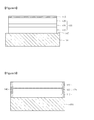
FIG. 1 is a side sectional view showing a semiconductor light emitting device according to a first embodiment; -
FIGS. 2 to 9 are side sectional views showing the manufacturing process of the semiconductor light emitting device according to the first embodiment ofFIG. 1 ; -
FIG. 10 is a side sectional view showing a semiconductor light emitting device according to a second embodiment; -
FIG. 11 is a side sectional view showing a semiconductor light emitting device according to a third embodiment; and -
FIG. 12 is a side sectional view showing a semiconductor light emitting device according to a fourth embodiment. - Hereinafter, a semiconductor light emitting device according to the embodiments will be described in detail with reference to accompanying drawings. In the following description, the thickness and size of each layer shown in the drawings can be exaggerated, omitted or schematically drawn for the purpose of convenience or clarity. In addition, the top or the bottom of each layer will be determined on the basis of the drawings.
- In the description of the embodiments, it will be understood that, when a layer (or film), a region, a pattern, or a structure is referred to as being "on" or "under" another substrate, another layer (or film), another region, another pad, or another pattern, it can be "directly" or "indirectly" on the other substrate, layer (or film), region, pad, or pattern, or one or more intervening layers may also be present. Such a position of the layer has been described with reference to the drawings.
-
FIG. 1 is a side sectional view showing a semiconductor light emitting device according to a first embodiment. - Referring to
FIG. 1 , the semiconductorlight emitting device 100 includes a firstconductive semiconductor layer 110, anactive layer 120, a secondconductive semiconductor layer 130, aninsulating layer 140, asecond electrode layer 150, and aconductive support member 160. - The semiconductor
light emitting device 100 includes LEDs made of group III-V compound semiconductors, and the LEDs may include color LEDs to emit blue, green or red light, or UV LEDs. The emission light of the LEDs may be variously realized within the technical scope of the embodiment. - The first
conductive semiconductor layer 110 may include compound semiconductors of group III-V elements doped with first conductive dopants. For instance, the firstconductive semiconductor layer 110 may be selected from the group consisting of GaN, AlN, AlGaN, InGaN, InN, InAlGaN, AlInN, AlGaAs, GaP, GaAs, GaAsP, and AlGaInP. - If the first
conductive semiconductor layer 110 includes an N type semiconductor layer, the first conductive dopant may include an N type dopant such as Si, Ge, Sn, Se, or Te. The firstconductive semiconductor layer 110 may serve as an electrode contact layer, and may have a single-layer structure or a multi-layer structure, but the embodiment is not limited thereto. - A
first electrode 170 is formed on the firstconductive semiconductor layer 110, and thefirst electrode 170 supplies power having first polarity. A roughness (not shown) having a predetermined shape may be formed on a top surface of the firstconductive semiconductor layer 110, and the roughness may be additionally provided or modified within the technical scope of the embodiment. - In addition, a transmissive electrode layer (not shown) may be formed on the first
conductive semiconductor layer 110, and spreads the power having the first polarity, which has been supplied by thefirst electrode 170, onto the whole region. The transmissive electrode layer may include at least one selected from the group consisting of ITO(indium tin oxide), IZO(indium zinc oxide), IZTO(indium zinc tin oxide), IAZO(indium aluminum zinc oxide), IGZO(indium gallium zinc oxide), IGTO(indium gallium tin oxide), AZO(aluminum zinc oxide), ATO(antimony tin oxide), GZO(gallium zinc oxide), IrOx, RuOx, RuOx/ITO, Ni/IrOx/Au, and Ni/IrOx/Au/ITO. - The
active layer 120 is formed under the firstconductive semiconductor layer 110, and may have a single quantum well structure or a multiple quantum well structure. Theactive layer 120 may have a stack structure including a well layer and a barrier layer, which are made from group III-V compound semiconductor material. For instance, theactive layer 120 may have a stack structure of InGaN well/GaN barrier layers. - The
active layer 120 is made of material having band gap energy according to wavelengths of light to be emitted. Theactive layer 120 may include material capable of providing color light such as blue light, red light, or green light, but the embodiment is not limited thereto. A conductive clad layer may be formed on and/or under theactive layer 120. The conductive clad layer may include an AlGaN layer. - The second
conductive semiconductor layer 130 is provided under theactive layer 120. The secondconductive semiconductor layer 130 may include compound semiconductors of group III-V elements doped with the second conductive dopant. For instance, the secondconductive layer 130 may be selected from the group consisting of GaN, AlN, AlGaN, InGaN, InN, InAlGaN, AlInN, AlGaAs, GaP, GaAs, GaAsP, and AlGaInP. If the secondconductive semiconductor layer 130 is a P type semiconductor layer, the second conductive dopant includes a P type dopant such as Mg or Ze. The secondconductive semiconductor layer 130 may serve as an electrode contact layer, and may have a single-layer structure or a multi-layer structure, but the embodiment is not limited thereto. - The first
conductive semiconductor layer 110, theactive layer 120, and the secondconductive semiconductor layer 130 may be defined as alight emitting structure 135. The firstconductive semiconductor layer 110 may include a P type semiconductor, and the secondconductive semiconductor layer 130 may include an N type semiconductor. A third conductive semiconductor layer such as an N type semiconductor layer or a P type semiconductor layer may be formed under the secondconductive semiconductor layer 130. Accordingly, thelight emitting structure 135 may include at least one of an N-P junction structure, a P-N junction structure, an N-P-N junction structure and a P-N-P junction structure. - The
insulating layer 140 is formed on an outer peripheral surface of thelight emitting structure 135. Theinsulating layer 140 serves as a sidewall on the outer peripheral surface of the secondconductive semiconductor layer 130, theactive layer 120, and the firstconductive semiconductor layer 110. Theinsulating layer 140 may be formed in the shape of a band or a ring. - The
insulating layer 140 may include insulating material such as SiO2, Si3N4, Al2O3, or TiO2, but the embodiment is not limited thereto. - The
insulating layer 140 may be formed as a sidewall on an outer peripheral surface of at least one semiconductor layer. For instance, theinsulating layer 140 may be formed on an outer peripheral surface of theactive layer 120 or both the secondconductive semiconductor layer 130 and theactive layer 120. - In addition, an upper end of the
insulating layer 140 may extend to a lower portion of the firstconductive semiconductor layer 110. A lower end of the insulatinglayer 140 may extend downward beyond the secondconductive semiconductor layer 130. - The insulating
layer 140 may have a thickness less than or equal to that of thelight emitting structure 135, or may have a thickness greater than or equal to that of thelight emitting structure 135. - The
second electrode layer 150 may be formed under the secondconductive semiconductor layer 130, or may extend to a lower portion of the insulatinglayer 140. - The
second electrode layer 150 may include Ag, Ni, Al, Rh, Pd, Ir, Ru, Mg, Zn, Pt, Au, Hf, or the combination thereof. Thesecond electrode layer 150 may include reflective electrode material having 50% or more of a reflective rate. - An ohmic contact layer (not shown) having a plurality of patterns arranged in the form of a matrix and/or a layer may be interposed between the
second electrode layer 150 and the secondconductive semiconductor layer 130. The ohmic contact layer includes at least one selected from the group consisting of ITO, IZO, AZO, IZTO, IAZO, IGZO, IGTO, and ATO. - The
second electrode layer 150 may make schottky contact with the secondconductive semiconductor layer 130 or make ohmic contact with the secondconductive semiconductor layer 130. If an ohmic contact layer having a pattern exists between thesecond electrode layer 150 and the secondconductive semiconductor layer 130, thesecond electrode layer 150 may make schottky contact with the secondconductive semiconductor layer 130, and the ohmic contact layer makes ohmic contact with the secondconductive semiconductor layer 130. Accordingly, since thesecond electrode layer 150 has an electric characteristic different from that of the ohmic contact layer, current supplied to the secondconductive semiconductor layer 130 can be diffused. - The
second electrode layer 150 stably supplies power having the second polarity to thelight emitting structure 135, and reflects light incident through the secondconductive semiconductor layer 130. - The
conductive support member 160 is formed under thesecond electrode layer 150. The secondconductive support member 160 may be realized by using Cu, Au, Ni, Mo, Cu-W, and carrier wafers such as Si, Ge, GaAs, ZnO, and SiC. Theconductive support member 160 may be formed through an electroplating process, but the embodiment is not limited thereto. - The
second electrode layer 150 and theconductive support member 160 may be used as a second electrode part to supply power having the second polarity to thelight emitting structure 135. The second electrode part may include electrode material in a single-layer structure or a multiple-layer structure, or may be bonded to a lower portion of the secondconductive semiconductor layer 130 by using an adhesive agent. - In the semiconductor
light emitting device 100, the insulatinglayer 140 is provided at an outer portion of thelight emitting structure 135, thereby preventing residual materials or external moisture from infiltrating into an outer portion of thelight emitting structure 135. Accordingly, electrical short among the semiconductor layers 110, 120, and 130 can be prevented from occurring at the outer portion of the semiconductorlight emitting device 100. - The insulating
layer 140 is provided at an outer portion of thelight emitting structure 135, thereby preventing current from leaking out of thelight emitting structure 135. For instance, current applied through thesecond electrode layer 150 has tendency to be directed to the outside of thelight emitting structure 135. However, such current is shut off by the insulatinglayer 140, so that current injection efficiency can be improved. - The insulating
layer 140 is provided at outer portions of thesecond electrode layer 150 and the secondconductive semiconductor layer 130, so that the adhesion strength of thesecond electrode layer 150 can be improved. -
FIGS. 2 to 9 are sectional views showing the manufacturing process of the semiconductor light emitting device according to the first embodiment. - Referring to
FIG. 2 , the firstconductive semiconductor layer 110 is formed on asubstrate 101, and theactive layer 120 is formed on the firstconductive semiconductor layer 110. The secondconducive semiconductor layer 130 is formed on theactive layer 120. - The
substrate 101 may be selected from the group consisting of a sapphire substrate (Al2O3), GaN, SiC, ZnO, Si, GaP, InP, Ga203, and GaAs. A concave-convex pattern may be formed on the surface of thesubstrate 101, but the embodiment is not limited thereto. - A group III-V compound semiconductor may be grown on the
substrate 101, and growth equipment may be selected from the group consisting of an E-beam evaporator, PVD (physical vapor deposition), CVD (chemical vapor deposition), PLD (plasma laser deposition), dual-type thermal evaporator, sputtering, and MOCVD (metal organic chemical vapor deposition). However, the embodiment is not limited thereto. - A buffer layer (not shown) and/or an undoped semiconductor layer (not shown) may be formed between the
substrate 101 and the firstconductive semiconductor layer 110 by using a compound semiconductor of group III-V elements, and may be separated or removed from thesubstrate 101 after a thin film has been grown. The buffer layer can reduce a lattice constant mismatch with respect to thesubstrate 101, and the undoped semiconductor layer may be a base to grow a compound semiconductor layer. - The first
conductive semiconductor layer 110 may include a compound semiconductor of group III-V elements doped with the first conductive dopant. For example, the firstconductive semiconductor layer 110 may be selected from the group consisting of GaN, AlN, AlGaN, InGaN, InN, InAlGaN, AlInN, AlGaAs, GaP, GaAs, GaAsP, and AlGaInP. If the firstconductive semiconductor layer 110 is an N-type semiconductor layer, the first conductive dopant includes an N type dopant such as Si, Ge, Sn, Se, or Te. The firstconductive semiconductor layer 110 may serve as an electrode contact layer, and may have a single-layer structure or a multiple-layer structure. However, the embodiment is not limited thereto. - The
active layer 120 may have a single quantum well structure or a multiple quantum well structure. Theactive layer 120 may have a stack structure including well and barrier layers which are made of a compound semiconductor of group III-V elements. For instance, theactive layer 120 may have a stack structure of InGaN well/GaN barrier layers. A conductive clad layer may be formed on and/or under theactive layer 120, and may include an AlGaN layer. - The second
conductive semiconductor layer 130 is formed on theactive layer 120. The secondconductive semiconductor layer 130 may include a compound semiconductor of group III-V elements doped with the second conductive dopant. For instance, the secondconductive semiconductor layer 130 may be selected from the group consisting of GaN, AIN, AlGaN, InGaN, InN, InAlGaN, AlInN, AlGaAs, GaP, GaAs, GaAsP, and AlGaInP. If the secondconductive semiconductor layer 130 is a P type semiconductor layer, the second conductive dopant is a P type dopant such as Mg or Ze. The secondconductive semiconductor layer 130 may serve as an electrode contact layer, and may have a single-layer structure or a multi-layer structure, but the embodiment is not limited thereto. - The first
conductive semiconductor layer 110, theactive layer 120, and the secondconductive semiconductor layer 130 may be defined as thelight emitting structure 135. The firstconductive semiconductor layer 110 may include a P type semiconductor, and the secondconductive semiconductor layer 130 may include an N type semiconductor. A third conductive semiconductor layer such as an N type semiconductor layer or a P type semiconductor layer may be formed on the secondconductive semiconductor layer 130. Accordingly, thelight emitting structure 135 may include at least one of an N-P junction structure, a P-N junction structure, an N-P-N junction structure, and a P-N-P junction structure. - Referring to
FIGS. 3 and4 , amask layer 145 is formed on an inner region (light emission region) of the secondconductive semiconductor layer 130. - The
mask layer 145 is formed on the secondconductive semiconductor layer 130 through a photolithography process, and an outerperipheral surface 146 of the secondconductive semiconductor layer 130 may be etched in a predetermined mask pattern. Accordingly, themask layer 145 is formed at the inner region of the secondconductive semiconductor layer 130 except for the outerperipheral surface 146 of the secondconductive semiconductor layer 130. To form themask layer 145, various schemes may be used within the technical scope of the embodiment. However, the embodiment is not limited thereto. - A first mesa etching process may be performed with respect to the outer
peripheral surface 146 of the secondconductive semiconductor layer 130. The first mesa etching process may include a dry and/or wet etching process. Equipment for the dry etching process includes an ICP (Inductively Coupled Plasma), but the embodiment is not limited thereto. - The etching depth D1 of the first mesa etching process may correspond to a depth from the second
conductive semiconductor layer 130 to a position in which thesubstrate 101 or the firstconductive semiconductor layer 110 is exposed. The etching depth D1 of the first mesa etching process may be formed with respect to at least one of the semiconductor layers 130, 120, and 110 of thelight emitting structure 135 or all of the semiconductor layers 130, 120, and 110. - Referring to
FIGS. 4 and 5 , the insulatinglayer 140 is formed at aregion 147 which has been formed through the first mesa etching process. The insulatinglayer 140 may include insulating material such as SiO2, Si3N4, Al2O3, or TiO2, but the embodiment is not limited thereto. - The insulating
layer 140 is formed as a sidewall on the outer peripheral surface of the secondconductive semiconductor layer 130, theactive layer 120, and the firstconductive semiconductor layer 110, and may be formed in the shape of a band or a ring. - The insulating
layer 140 is provided at on the outer peripheral surface of the semiconductor layers 130, 120, and 110, thereby preventing residual material or external moisture from infiltrating into outer portions of the semiconductor layers 130, 120, and 110. Accordingly, electrical short can be prevented from occurring among the semiconductor layers 110, 120, and 130. - The upper end of the insulating
layer 140 may protrude upward beyond the secondconductive semiconductor layer 130. The insulatinglayer 140 may have a thickness less than or equal to that of thelight emitting structure 135, or may have a thickness greater than or equal to that of thelight emitting structure 135. - After the insulating
layer 140 has been formed, the mask layer (see 145 ofFIG. 3 ) is removed. -
FIG. 6 is a plan view showing a plurality of chip regions. The insulatinglayer 140 may be formed in the shape of a polygonal band or ring on the outer peripheral surface of each chip. A central line L1 of the insulatinglayer 140 becomes a chip boundary region used to cut thesubstrate 101 in chip size. - Referring to
FIG. 7 , thesecond electrode layer 150 is formed on the secondconductive semiconductor layer 130. Thesecond electrode layer 150 may be formed on the secondconductive semiconductor layer 130, or may be formed on the secondconductive semiconductor layer 130 and the insulatinglayer 140. - The
second electrode layer 150 may include Ag, Ni, Al, Rh, Pd, Ir, Ru, Mg, Zn, Pt, Au, Hf, or the combination thereof. In this case, thesecond electrode layer 150 may include reflective electrode material having 50% or more of a reflective rate. - An ohmic contact layer (not shown) having a plurality of patterns arranged in the form of a matrix and/or a layer may be interposed between the
second electrode layer 150 and the secondconductive semiconductor layer 130. The ohmic contact layer includes at least one selected from the group consisting of ITO, IZO, AZO, IZTO, IAZO, IGZO, IGTO, and ATO. - The
second electrode layer 150 may make schottky contact with the secondconductive semiconductor layer 130 or may make ohmic contact with the secondconductive semiconductor layer 130. If an ohmic contact layer having a pattern exists between thesecond electrode layer 150 and the secondconductive semiconductor layer 130, thesecond electrode layer 150 makes schottky contact with the secondconductive semiconductor layer 130, and the ohmic contact layer makes ohmic contact with the secondconductive semiconductor layer 130. Accordingly, since thesecond electrode layer 150 has an electric characteristic different from that of the ohmic contact layer, current supplied to the secondconductive semiconductor layer 130 can be diffused. - The
second electrode layer 150 stably supplies power having the second polarity to thelight emitting structure 135, and reflects light incident through the secondconductive semiconductor layer 130. - Referring to
FIG. 8 , theconductive support member 160 is formed on thesecond electrode layer 150. The secondconductive support member 160 may be realized by using Cu, Au, Ni, Mo, Cu-W, and carrier wafers such as Si, Ge, GaAs, ZnO, and SiC. Theconductive support member 160 may be formed through an electroplating process, but the embodiment is not limited thereto. - The
second electrode layer 150 and theconductive support member 160 may be used as the second electrode part to supply power having the second polarity to thelight emitting structure 135. The second electrode part may include electrode material having a single-layer structure or a multiple-layer structure, or may be bonded to a lower portion of the secondconductive semiconductor layer 130 by using an adhesive agent. - When the
conductive support member 160 has been formed, the resultant structure is turned over such that thesubstrate 101 is located at the uppermost layer and theconductive support member 160 serves as a base. - The
substrate 101 is separated from the firstconductive semiconductor layer 110 by irradiating a laser beam having a predetermined wavelength through thesubstrate 101. In other words, thesubstrate 101 may be removed through an LLO (Laser Lift Off) process. If another semiconductor layer (e.g., buffer layer) is formed between thesubstrate 101 and the firstconductive semiconductor layer 110, the buffer layer is removed through a wet etching scheme, thereby separating thesubstrate 101 from the firstconductive semiconductor layer 110. The substrate removing scheme is only one example, and thesubstrate 101 may be removed through various schemes. - In addition, the insulating
layer 140 is provided at outer portions of the secondconductive semiconductor layer 130 and thesecond electrode layer 150, so that adhesion strength between the secondconductive semiconductor layer 130 and thesecond electrode layer 150 can be enhanced. Accordingly, the secondconductive semiconductor layer 130 and thesecond electrode layer 150 can be protected from external impact. Therefore, the electrical reliability for the semiconductor light emitting device can be improved. - In addition, the insulating
layer 140 can reduce impact caused by a laser beam when the laser beam is transmitted. - The surface of the first
conductive semiconductor layer 110 without thesubstrate 101 may be polished through ICP/RIE (Inductively coupled Plasma/Reactive Ion Etching). - A roughness may be formed on the surface of the first
conductive semiconductor layer 110. - Referring to
FIG. 9 , thefirst electrode 170 is formed on the firstconductive semiconductor layer 110. - In this case, a second mesa etching process is performed. The second mesa etching process is to etch the central portion of the insulating
layer 140 provided on the outer peripheral surface of each chip. In other words, the second mesa etching process is performed along the chip boundary line L1 at a predetermined depth. The second mesa etching process may include a dry etching scheme or a wet etching scheme. - The
first electrode 170 may be formed before or after the first mesa etching process is performed. Before thefirst electrode 170 is formed, a transmissive conductive layer (not shown) including ITO may be formed on the firstconductive semiconductor layer 110. The transmissive conductive layer diffuses current supplied through thefirst electrode 170. - After the second mesa etching process has been performed, the structure is divided to an individual chip through a breaking process.
- Since the insulating
layer 140 is etched through the second mesa etching process, electrical short caused by the etching for the semiconductor material can be prevented. In other word, the stability of the manufacturing process can be improved. Accordingly, light emission efficiency can be improved by the ohmic characteristic of the insulatinglayer 140. - Since the insulating
layer 140 has been formed, an additional insulating layer to protect an outer portion of thelight emitting structure 135 from an external environment is omitted. -
FIG. 10 is a side sectional view showing a semiconductor light emitting device according to a second embodiment. Hereinafter, the second embodiment will be described while focusing on the difference from the first embodiment in order to avoid redundancy. - Referring to
FIG. 10 , a semiconductorlight emitting device 100A includes an insulatinglayer 142 formed on an outer peripheral surface of thelight emitting structure 135. The insulatinglayer 142 may be formed at a thickness D2 from the secondconductive semiconductor layer 130 to a portion of the firstconductive semiconductor layer 110. The insulatinglayer 142 can perform a function the same as that of the insulatinglayer 140 according to the first embodiment even if the insulatinglayer 142 is not formed over the whole area of an outer portion of the firstconductive semiconductor layer 110. - A point P1 of an upper end of the insulating
layer 142 may vary according to the etching depth of the first mesa etching process. - In addition, the insulating
layer 142 may be formed at a thickness D3 less than or equal to that of theactive layer 120. For example, the insulatinglayer 142 may be formed from theactive layer 120 to the secondconductive semiconductor layer 130 or the third conductive semiconductor layer (not shown). - In the semiconductor
light emitting device 100A, the insulatinglayer 142 has material, a function, and an effect the same as those of the insulatinglayer 140 according to the first embodiment. -
FIG. 11 is a side sectional view showing a semiconductor light emitting device according to a third embodiment. Hereinafter, the third embodiment will be described while focusing on the difference from the first embodiment in order to avoid redundancy. - Referring to
FIG. 11 , the semiconductorlight emitting device 100B includes an insulatinglayer 144 formed on an outer peripheral surface of thelight emitting structure 135 and thesecond electrode layer 150. - The insulating
layer 144 may be formed on an outer peripheral surface of theactive layer 120, the secondconductive semiconductor layer 130, and thesecond electrode layer 150. - The insulating
layer 144 may protrude downward from the secondconductive semiconductor layer 130 at a predetermined thickness D4, so that the insulatinglayer 144 may be provided at an outer portion of thesecond electrode layer 150. - The
second electrode layer 150 may be formed under the secondconductive semiconductor layer 130, or may be formed under both of the secondconductive semiconductor layer 130 and the insulatinglayer 144. - Since the insulating
layer 144 places the outer portion of thesecond electrode layer 150 at a lower position to more increase the distance between thesecond electrode layer 150 and the semiconductor layers 110, 120, and 130. The above structure can improve the electrical reliability for the semiconductorlight emitting device 100B. - An upper end of the insulating
layer 144 may extend to a portion of the firstconductive semiconductor layer 110 or an upper end of the firstconductive semiconductor layer 110, but the embodiment is not limited thereto. - In the semiconductor
light emitting device 100B, the insulatinglayer 144 has material, a function, and an effect the same as those of the insulatinglayer 140 according to the first embodiment. -
FIG. 12 is a side sectional view showing a semiconductor light emitting device according to a fourth embodiment. Hereinafter, the fourth embodiment will be described while focusing on the difference from the first and second embodiments in order to avoid redundancy. - Referring to
FIG. 12 , a semiconductorlight emitting device 100C includes the insulatinglayer 142 formed on an outer peripheral surface of thelight emitting structure 135, and includes apassivation layer 155 formed on an outer peripheral surface of a top surface of thesecond electrode layer 150. - The
passivation layer 155 may be formed in the shape of a band or a ring along an outer peripheral surface between thesecond electrode 150 and the insulatinglayer 142. Thepassivation layer 155 may make contact with an outer peripheral surface of a bottom surface of the secondconductive semiconductor layer 130. If thepassivation layer 155 includes conductive material, the electrical characteristic of thepassivation layer 155 can be used. - In addition, the
passivation layer 155 may include insulating material the same as that of the insulatinglayer 142 or may include a transmissive conductive layer. If thepassivation layer 155 is the transmissive conductive layer, thepassivation layer 155 may include ITO, IZO, AZO, IZTO, IAZO, IGZO, IGTO, or ATO. - Since the
passivation layer 155 is formed at a chip boundary region, thepassivation layer 155 can minimize the impact transferred to thelight emitting structure 135 when the substrate is separated. If thepassivation layer 155 is a transmissive conductive layer, thepassivation layer 155 can reduce the width of the insulatinglayer 142 to increase the light emission area. - The technical characteristics of each embodiment are applicable to another embodiment, and are not limited to each embodiment.
- Although the exemplary embodiments of the present invention have been described, it is understood that the present invention should not be limited to these exemplary embodiments but various changes and modifications can be made by one ordinary skilled in the art within the spirit and scope of the present invention as hereinafter claimed.
- The embodiment can provide a semiconductor light emitting device such as an LED.
- The embodiment can improve the reliability for the manufacturing process of the semiconductor light emitting device.
- According to the embodiment, a light source formed by packaging the semiconductor light emitting device is applicable to various fields such as lighting, indicators, and displays.
Claims (15)
- A semiconductor light emitting device comprising:a first conductive semiconductor layer;an active layer under the first conductive semiconductor layer;a second conductive semiconductor layer under the active layer;an insulating layer on an outer peripheral surface of at least the active layer among the first conductive semiconductor layer, the active layer, and the second conductive semiconductor layer; anda second electrode layer under the second conductive semiconductor layer.
- The semiconductor light emitting device of claim 1, further comprising:
a first electrode on the first conductive semiconductor layer; and
a conductive support member under the second electrode layer. - The semiconductor light emitting device of claim 1, wherein the insulating layer is formed on an outer peripheral surface of both of the second conductive semiconductor layer and the active layer.
- The semiconductor light emitting device of claim 1, wherein the second electrode layer includes a reflective electrode layer under the second conductive semiconductor layer and the insulating layer.
- The semiconductor light emitting device of claim 1, wherein the insulating layer extends from an outer portion of the second conductive semiconductor layer to a part of an outer portion of the first conductive semiconductor layer or over a whole area of the outer portion of the first conductive semiconductor layer.
- The semiconductor light emitting device of claim 5, wherein the insulating layer is formed on an outer peripheral surface of the electrode layer.
- The semiconductor light emitting device of claim 1, wherein the insulating layer includes at least one selected from the group consisting of SiO2, Si3N4, Al2O3, and TiO2.
- The semiconductor light emitting device of claim 3, further comprising a passivation layer between the insulating layer and the second electrode layer.
- The semiconductor light emitting device of claim 1, wherein the insulating layer has a band shape or a ring shape.
- A semiconductor light emitting device comprising:a light emitting structure including a first conductive semiconductor layer, an active layer under the first conductive semiconductor layer, and a second conductive semiconductor layer under the active layer;a first electrode on the first conductive semiconductor layer;a second electrode layer under the second conductive semiconductor layer; andan insulating layer on an outer peripheral surface of both of the active layer and the second conductive semiconductor layer.
- The semiconductor light emitting device of claim 10, wherein the insulating layer is interposed between the first conductive semiconductor layer and the second electrode layer.
- The semiconductor light emitting device of claim 10, further comprising:a conductive support member under the second electrode layer; andan ohmic contact layer having a plurality of patterns between the second electrode layer and the second conductive semiconductor layer.
- The semiconductor light emitting device of claim 10, further comprising a third conductive semiconductor layer between the second conductive semiconductor layer and the second electrode layer, wherein the insulating layer is formed on an outer peripheral surface of the third conductive semiconductor layer.
- The semiconductor light emitting device of claim 10, further comprising a transmissive conductive layer on an outer peripheral surface between the second conductive semiconductor layer and the second electrode layer, wherein the transmissive conductive layer has a band shape or a ring shape.
- The semiconductor light emitting device of claim 10, wherein the insulating layer extends from a part of an outer portion of the first conductive semiconductor layer to an outer portion of the second conductive semiconductor layer.
Applications Claiming Priority (2)
| Application Number | Priority Date | Filing Date | Title |
|---|---|---|---|
| KR1020080045740A KR20090119596A (en) | 2008-05-16 | 2008-05-16 | Semiconductor light emitting device and manufacturing method thereof |
| PCT/KR2009/002596 WO2009139603A2 (en) | 2008-05-16 | 2009-05-15 | Semiconductor light-emitting device |
Publications (3)
| Publication Number | Publication Date |
|---|---|
| EP2290709A2 true EP2290709A2 (en) | 2011-03-02 |
| EP2290709A4 EP2290709A4 (en) | 2012-10-10 |
| EP2290709B1 EP2290709B1 (en) | 2016-08-17 |
Family
ID=41319183
Family Applications (1)
| Application Number | Title | Priority Date | Filing Date |
|---|---|---|---|
| EP09746782.3A Active EP2290709B1 (en) | 2008-05-16 | 2009-05-15 | Semiconductor light-emitting device |
Country Status (5)
| Country | Link |
|---|---|
| US (2) | US8530919B2 (en) |
| EP (1) | EP2290709B1 (en) |
| KR (1) | KR20090119596A (en) |
| CN (1) | CN102027606B (en) |
| WO (1) | WO2009139603A2 (en) |
Families Citing this family (9)
| Publication number | Priority date | Publication date | Assignee | Title |
|---|---|---|---|---|
| KR101039896B1 (en) * | 2009-12-03 | 2011-06-09 | 엘지이노텍 주식회사 | Light emitting device and manufacturing method |
| KR100999798B1 (en) * | 2010-02-11 | 2010-12-08 | 엘지이노텍 주식회사 | Semiconductor light emitting device and manufacturing method thereof |
| KR20110123118A (en) * | 2010-05-06 | 2011-11-14 | 삼성전자주식회사 | Vertical light emitting device with patterned light emitting part |
| KR101799451B1 (en) * | 2011-06-02 | 2017-11-20 | 엘지이노텍 주식회사 | A light emitting device |
| KR102092911B1 (en) * | 2014-03-28 | 2020-03-24 | 동우 화인켐 주식회사 | Soft etching agent of semiconductor light emitting layer, light emitting element and display element |
| KR101771461B1 (en) * | 2015-04-24 | 2017-08-25 | 엘지전자 주식회사 | Display device using semiconductor light emitting device and method for manufacturing the same |
| KR101771463B1 (en) * | 2016-07-15 | 2017-08-25 | 엘지전자 주식회사 | Display device using semiconductor light emitting device |
| KR102271031B1 (en) * | 2019-10-15 | 2021-06-30 | (재)한국나노기술원 | a high efficiency micro LED device using insulator electron affinity |
| CN110911536A (en) * | 2019-12-13 | 2020-03-24 | 深圳第三代半导体研究院 | A Micro-LED chip and its manufacturing method |
Family Cites Families (15)
| Publication number | Priority date | Publication date | Assignee | Title |
|---|---|---|---|---|
| JP3723434B2 (en) * | 1999-09-24 | 2005-12-07 | 三洋電機株式会社 | Semiconductor light emitting device |
| US6900069B2 (en) | 2001-03-09 | 2005-05-31 | Seiko Epson Corporation | Method of fabricating surface-emission type light-emitting device, surface-emitting semiconductor laser, method of fabricating the same, optical module and optical transmission device |
| CN1848564A (en) * | 2001-03-09 | 2006-10-18 | 精工爱普生株式会社 | Manufacturing method of light-emitting element, semiconductor laser and manufacturing method thereof |
| TWI278995B (en) * | 2002-01-28 | 2007-04-11 | Nichia Corp | Nitride semiconductor element with a supporting substrate and a method for producing a nitride semiconductor element |
| JP2006100500A (en) | 2004-09-29 | 2006-04-13 | Sanken Electric Co Ltd | Semiconductor light emitting device and manufacturing method thereof |
| KR101203137B1 (en) * | 2004-10-22 | 2012-11-20 | 학교법인 포항공과대학교 | GaN compound semiconductor light emitting element and method of manufacturing the same |
| CN100561758C (en) * | 2004-10-22 | 2009-11-18 | 首尔Opto仪器股份有限公司 | Gallium nitride compound semiconductor light-emitting element and method for manufacturing same |
| KR100638819B1 (en) * | 2005-05-19 | 2006-10-27 | 삼성전기주식회사 | Vertical nitride semiconductor light emitting device with improved light extraction efficiency |
| KR101154744B1 (en) | 2005-08-01 | 2012-06-08 | 엘지이노텍 주식회사 | Nitride light emitting device and fabrication method thereof |
| JP5016808B2 (en) | 2005-11-08 | 2012-09-05 | ローム株式会社 | Nitride semiconductor light emitting device and method for manufacturing nitride semiconductor light emitting device |
| JP2008053685A (en) * | 2006-08-23 | 2008-03-06 | Samsung Electro Mech Co Ltd | Vertical structure gallium nitride based light-emitting diode device and method of manufacturing the same |
| KR100856089B1 (en) * | 2006-08-23 | 2008-09-02 | 삼성전기주식회사 | Vertically structured GaN type Light Emitting Diode device And Manufacturing Method thereof |
| KR101371511B1 (en) * | 2007-10-04 | 2014-03-11 | 엘지이노텍 주식회사 | Light emitting device having vertical topology |
| CN102017193B (en) | 2008-03-25 | 2012-05-30 | 晶能光电(江西)有限公司 | Semiconductor light-emitting device with double-sided passivation |
| KR100992657B1 (en) | 2009-02-16 | 2010-11-05 | 엘지이노텍 주식회사 | Semiconductor light emitting device and manufacturing method thereof |
-
2008
- 2008-05-16 KR KR1020080045740A patent/KR20090119596A/en not_active Ceased
-
2009
- 2009-05-15 US US12/992,950 patent/US8530919B2/en active Active
- 2009-05-15 CN CN2009801176605A patent/CN102027606B/en active Active
- 2009-05-15 EP EP09746782.3A patent/EP2290709B1/en active Active
- 2009-05-15 WO PCT/KR2009/002596 patent/WO2009139603A2/en not_active Ceased
-
2013
- 2013-08-09 US US13/963,724 patent/US8766308B2/en active Active
Also Published As
| Publication number | Publication date |
|---|---|
| US8530919B2 (en) | 2013-09-10 |
| US20110062480A1 (en) | 2011-03-17 |
| WO2009139603A2 (en) | 2009-11-19 |
| US20130320389A1 (en) | 2013-12-05 |
| US8766308B2 (en) | 2014-07-01 |
| CN102027606B (en) | 2013-04-24 |
| CN102027606A (en) | 2011-04-20 |
| EP2290709A4 (en) | 2012-10-10 |
| EP2290709B1 (en) | 2016-08-17 |
| KR20090119596A (en) | 2009-11-19 |
| WO2009139603A3 (en) | 2010-02-18 |
Similar Documents
| Publication | Publication Date | Title |
|---|---|---|
| US8022428B2 (en) | Semiconductor light emitting device | |
| US8129727B2 (en) | Semiconductor light emitting device | |
| US8766308B2 (en) | Semiconductor light-emitting device | |
| US8614457B2 (en) | Semiconductor light emitting device | |
| EP2311108B1 (en) | Semiconductor light emitting device | |
| US8471286B2 (en) | Semiconductor light emitting device | |
| EP2262010A2 (en) | Semiconductor light-emitting device | |
| EP2317575B1 (en) | Semiconductor light emitting device and method for manufacturing same | |
| US20140332836A1 (en) | Semiconductor light emitting device | |
| KR20100093341A (en) | Semiconductor light emitting device and fabrication method thereof | |
| KR101500027B1 (en) | Semiconductor light emitting device | |
| KR20150142738A (en) | Light emitting device and lighting system | |
| KR20160054331A (en) | Light emitting device and light emitting device package thereof |
Legal Events
| Date | Code | Title | Description |
|---|---|---|---|
| PUAI | Public reference made under article 153(3) epc to a published international application that has entered the european phase |
Free format text: ORIGINAL CODE: 0009012 |
|
| 17P | Request for examination filed |
Effective date: 20101130 |
|
| AK | Designated contracting states |
Kind code of ref document: A2 Designated state(s): AT BE BG CH CY CZ DE DK EE ES FI FR GB GR HR HU IE IS IT LI LT LU LV MC MK MT NL NO PL PT RO SE SI SK TR |
|
| AX | Request for extension of the european patent |
Extension state: AL BA RS |
|
| DAX | Request for extension of the european patent (deleted) | ||
| A4 | Supplementary search report drawn up and despatched |
Effective date: 20120906 |
|
| RIC1 | Information provided on ipc code assigned before grant |
Ipc: H01L 33/44 20100101AFI20120831BHEP |
|
| 17Q | First examination report despatched |
Effective date: 20130503 |
|
| REG | Reference to a national code |
Ref country code: DE Ref legal event code: R079 Ref document number: 602009040448 Country of ref document: DE Free format text: PREVIOUS MAIN CLASS: H01L0033000000 Ipc: H01L0033200000 |
|
| GRAP | Despatch of communication of intention to grant a patent |
Free format text: ORIGINAL CODE: EPIDOSNIGR1 |
|
| RIC1 | Information provided on ipc code assigned before grant |
Ipc: H01L 33/42 20100101ALI20160217BHEP Ipc: H01L 33/20 20100101AFI20160217BHEP Ipc: H01L 33/38 20100101ALI20160217BHEP Ipc: H01L 33/44 20100101ALI20160217BHEP |
|
| INTG | Intention to grant announced |
Effective date: 20160307 |
|
| GRAS | Grant fee paid |
Free format text: ORIGINAL CODE: EPIDOSNIGR3 |
|
| GRAA | (expected) grant |
Free format text: ORIGINAL CODE: 0009210 |
|
| AK | Designated contracting states |
Kind code of ref document: B1 Designated state(s): AT BE BG CH CY CZ DE DK EE ES FI FR GB GR HR HU IE IS IT LI LT LU LV MC MK MT NL NO PL PT RO SE SI SK TR |
|
| REG | Reference to a national code |
Ref country code: GB Ref legal event code: FG4D |
|
| REG | Reference to a national code |
Ref country code: CH Ref legal event code: EP |
|
| REG | Reference to a national code |
Ref country code: IE Ref legal event code: FG4D |
|
| REG | Reference to a national code |
Ref country code: AT Ref legal event code: REF Ref document number: 821805 Country of ref document: AT Kind code of ref document: T Effective date: 20160915 |
|
| REG | Reference to a national code |
Ref country code: DE Ref legal event code: R096 Ref document number: 602009040448 Country of ref document: DE |
|
| REG | Reference to a national code |
Ref country code: NL Ref legal event code: FP |
|
| REG | Reference to a national code |
Ref country code: LT Ref legal event code: MG4D |
|
| REG | Reference to a national code |
Ref country code: AT Ref legal event code: MK05 Ref document number: 821805 Country of ref document: AT Kind code of ref document: T Effective date: 20160817 |
|
| PG25 | Lapsed in a contracting state [announced via postgrant information from national office to epo] |
Ref country code: FI Free format text: LAPSE BECAUSE OF FAILURE TO SUBMIT A TRANSLATION OF THE DESCRIPTION OR TO PAY THE FEE WITHIN THE PRESCRIBED TIME-LIMIT Effective date: 20160817 Ref country code: IT Free format text: LAPSE BECAUSE OF FAILURE TO SUBMIT A TRANSLATION OF THE DESCRIPTION OR TO PAY THE FEE WITHIN THE PRESCRIBED TIME-LIMIT Effective date: 20160817 Ref country code: LT Free format text: LAPSE BECAUSE OF FAILURE TO SUBMIT A TRANSLATION OF THE DESCRIPTION OR TO PAY THE FEE WITHIN THE PRESCRIBED TIME-LIMIT Effective date: 20160817 Ref country code: NO Free format text: LAPSE BECAUSE OF FAILURE TO SUBMIT A TRANSLATION OF THE DESCRIPTION OR TO PAY THE FEE WITHIN THE PRESCRIBED TIME-LIMIT Effective date: 20161117 Ref country code: HR Free format text: LAPSE BECAUSE OF FAILURE TO SUBMIT A TRANSLATION OF THE DESCRIPTION OR TO PAY THE FEE WITHIN THE PRESCRIBED TIME-LIMIT Effective date: 20160817 |
|
| PG25 | Lapsed in a contracting state [announced via postgrant information from national office to epo] |
Ref country code: ES Free format text: LAPSE BECAUSE OF FAILURE TO SUBMIT A TRANSLATION OF THE DESCRIPTION OR TO PAY THE FEE WITHIN THE PRESCRIBED TIME-LIMIT Effective date: 20160817 Ref country code: AT Free format text: LAPSE BECAUSE OF FAILURE TO SUBMIT A TRANSLATION OF THE DESCRIPTION OR TO PAY THE FEE WITHIN THE PRESCRIBED TIME-LIMIT Effective date: 20160817 Ref country code: SE Free format text: LAPSE BECAUSE OF FAILURE TO SUBMIT A TRANSLATION OF THE DESCRIPTION OR TO PAY THE FEE WITHIN THE PRESCRIBED TIME-LIMIT Effective date: 20160817 Ref country code: PT Free format text: LAPSE BECAUSE OF FAILURE TO SUBMIT A TRANSLATION OF THE DESCRIPTION OR TO PAY THE FEE WITHIN THE PRESCRIBED TIME-LIMIT Effective date: 20161219 Ref country code: PL Free format text: LAPSE BECAUSE OF FAILURE TO SUBMIT A TRANSLATION OF THE DESCRIPTION OR TO PAY THE FEE WITHIN THE PRESCRIBED TIME-LIMIT Effective date: 20160817 Ref country code: LV Free format text: LAPSE BECAUSE OF FAILURE TO SUBMIT A TRANSLATION OF THE DESCRIPTION OR TO PAY THE FEE WITHIN THE PRESCRIBED TIME-LIMIT Effective date: 20160817 Ref country code: GR Free format text: LAPSE BECAUSE OF FAILURE TO SUBMIT A TRANSLATION OF THE DESCRIPTION OR TO PAY THE FEE WITHIN THE PRESCRIBED TIME-LIMIT Effective date: 20161118 |
|
| REG | Reference to a national code |
Ref country code: FR Ref legal event code: PLFP Year of fee payment: 9 |
|
| PG25 | Lapsed in a contracting state [announced via postgrant information from national office to epo] |
Ref country code: RO Free format text: LAPSE BECAUSE OF FAILURE TO SUBMIT A TRANSLATION OF THE DESCRIPTION OR TO PAY THE FEE WITHIN THE PRESCRIBED TIME-LIMIT Effective date: 20160817 Ref country code: EE Free format text: LAPSE BECAUSE OF FAILURE TO SUBMIT A TRANSLATION OF THE DESCRIPTION OR TO PAY THE FEE WITHIN THE PRESCRIBED TIME-LIMIT Effective date: 20160817 |
|
| RAP2 | Party data changed (patent owner data changed or rights of a patent transferred) |
Owner name: LG INNOTEK CO., LTD. |
|
| REG | Reference to a national code |
Ref country code: DE Ref legal event code: R097 Ref document number: 602009040448 Country of ref document: DE |
|
| PG25 | Lapsed in a contracting state [announced via postgrant information from national office to epo] |
Ref country code: BE Free format text: LAPSE BECAUSE OF FAILURE TO SUBMIT A TRANSLATION OF THE DESCRIPTION OR TO PAY THE FEE WITHIN THE PRESCRIBED TIME-LIMIT Effective date: 20160817 Ref country code: SK Free format text: LAPSE BECAUSE OF FAILURE TO SUBMIT A TRANSLATION OF THE DESCRIPTION OR TO PAY THE FEE WITHIN THE PRESCRIBED TIME-LIMIT Effective date: 20160817 Ref country code: BG Free format text: LAPSE BECAUSE OF FAILURE TO SUBMIT A TRANSLATION OF THE DESCRIPTION OR TO PAY THE FEE WITHIN THE PRESCRIBED TIME-LIMIT Effective date: 20161117 Ref country code: CZ Free format text: LAPSE BECAUSE OF FAILURE TO SUBMIT A TRANSLATION OF THE DESCRIPTION OR TO PAY THE FEE WITHIN THE PRESCRIBED TIME-LIMIT Effective date: 20160817 Ref country code: DK Free format text: LAPSE BECAUSE OF FAILURE TO SUBMIT A TRANSLATION OF THE DESCRIPTION OR TO PAY THE FEE WITHIN THE PRESCRIBED TIME-LIMIT Effective date: 20160817 |
|
| PLBE | No opposition filed within time limit |
Free format text: ORIGINAL CODE: 0009261 |
|
| STAA | Information on the status of an ep patent application or granted ep patent |
Free format text: STATUS: NO OPPOSITION FILED WITHIN TIME LIMIT |
|
| PGFP | Annual fee paid to national office [announced via postgrant information from national office to epo] |
Ref country code: NL Payment date: 20170407 Year of fee payment: 9 |
|
| 26N | No opposition filed |
Effective date: 20170518 |
|
| PGFP | Annual fee paid to national office [announced via postgrant information from national office to epo] |
Ref country code: FR Payment date: 20170410 Year of fee payment: 9 |
|
| PG25 | Lapsed in a contracting state [announced via postgrant information from national office to epo] |
Ref country code: SI Free format text: LAPSE BECAUSE OF FAILURE TO SUBMIT A TRANSLATION OF THE DESCRIPTION OR TO PAY THE FEE WITHIN THE PRESCRIBED TIME-LIMIT Effective date: 20160817 Ref country code: LU Free format text: LAPSE BECAUSE OF NON-PAYMENT OF DUE FEES Effective date: 20170531 |
|
| REG | Reference to a national code |
Ref country code: CH Ref legal event code: PL |
|
| GBPC | Gb: european patent ceased through non-payment of renewal fee |
Effective date: 20170515 |
|
| PG25 | Lapsed in a contracting state [announced via postgrant information from national office to epo] |
Ref country code: MC Free format text: LAPSE BECAUSE OF FAILURE TO SUBMIT A TRANSLATION OF THE DESCRIPTION OR TO PAY THE FEE WITHIN THE PRESCRIBED TIME-LIMIT Effective date: 20160817 |
|
| REG | Reference to a national code |
Ref country code: IE Ref legal event code: MM4A |
|
| PG25 | Lapsed in a contracting state [announced via postgrant information from national office to epo] |
Ref country code: CH Free format text: LAPSE BECAUSE OF NON-PAYMENT OF DUE FEES Effective date: 20170531 Ref country code: LI Free format text: LAPSE BECAUSE OF NON-PAYMENT OF DUE FEES Effective date: 20170531 |
|
| PG25 | Lapsed in a contracting state [announced via postgrant information from national office to epo] |
Ref country code: LU Free format text: LAPSE BECAUSE OF NON-PAYMENT OF DUE FEES Effective date: 20170515 |
|
| PG25 | Lapsed in a contracting state [announced via postgrant information from national office to epo] |
Ref country code: GB Free format text: LAPSE BECAUSE OF NON-PAYMENT OF DUE FEES Effective date: 20170515 Ref country code: IE Free format text: LAPSE BECAUSE OF NON-PAYMENT OF DUE FEES Effective date: 20170515 |
|
| PG25 | Lapsed in a contracting state [announced via postgrant information from national office to epo] |
Ref country code: MT Free format text: LAPSE BECAUSE OF NON-PAYMENT OF DUE FEES Effective date: 20170515 |
|
| REG | Reference to a national code |
Ref country code: NL Ref legal event code: MM Effective date: 20180601 |
|
| PG25 | Lapsed in a contracting state [announced via postgrant information from national office to epo] |
Ref country code: FR Free format text: LAPSE BECAUSE OF NON-PAYMENT OF DUE FEES Effective date: 20180531 Ref country code: NL Free format text: LAPSE BECAUSE OF NON-PAYMENT OF DUE FEES Effective date: 20180601 |
|
| PG25 | Lapsed in a contracting state [announced via postgrant information from national office to epo] |
Ref country code: HU Free format text: LAPSE BECAUSE OF FAILURE TO SUBMIT A TRANSLATION OF THE DESCRIPTION OR TO PAY THE FEE WITHIN THE PRESCRIBED TIME-LIMIT; INVALID AB INITIO Effective date: 20090515 |
|
| PG25 | Lapsed in a contracting state [announced via postgrant information from national office to epo] |
Ref country code: CY Free format text: LAPSE BECAUSE OF NON-PAYMENT OF DUE FEES Effective date: 20160817 |
|
| PG25 | Lapsed in a contracting state [announced via postgrant information from national office to epo] |
Ref country code: MK Free format text: LAPSE BECAUSE OF FAILURE TO SUBMIT A TRANSLATION OF THE DESCRIPTION OR TO PAY THE FEE WITHIN THE PRESCRIBED TIME-LIMIT Effective date: 20160817 |
|
| PG25 | Lapsed in a contracting state [announced via postgrant information from national office to epo] |
Ref country code: TR Free format text: LAPSE BECAUSE OF FAILURE TO SUBMIT A TRANSLATION OF THE DESCRIPTION OR TO PAY THE FEE WITHIN THE PRESCRIBED TIME-LIMIT Effective date: 20160817 |
|
| PG25 | Lapsed in a contracting state [announced via postgrant information from national office to epo] |
Ref country code: IS Free format text: LAPSE BECAUSE OF FAILURE TO SUBMIT A TRANSLATION OF THE DESCRIPTION OR TO PAY THE FEE WITHIN THE PRESCRIBED TIME-LIMIT Effective date: 20161217 |
|
| REG | Reference to a national code |
Ref country code: DE Ref legal event code: R081 Ref document number: 602009040448 Country of ref document: DE Owner name: SUZHOU LEKIN SEMICONDUCTOR CO. LTD., TAICANG, CN Free format text: FORMER OWNER: LG INNOTEK CO., LTD., SEOUL, KR |
|
| REG | Reference to a national code |
Ref country code: DE Ref legal event code: R079 Ref document number: 602009040448 Country of ref document: DE Free format text: PREVIOUS MAIN CLASS: H01L0033200000 Ipc: H10H0020819000 |
|
| PGFP | Annual fee paid to national office [announced via postgrant information from national office to epo] |
Ref country code: DE Payment date: 20250408 Year of fee payment: 17 |