EP2287863A1 - Magnetic tunnel junction device and method for manufacturing the same - Google Patents
Magnetic tunnel junction device and method for manufacturing the same Download PDFInfo
- Publication number
- EP2287863A1 EP2287863A1 EP10162168A EP10162168A EP2287863A1 EP 2287863 A1 EP2287863 A1 EP 2287863A1 EP 10162168 A EP10162168 A EP 10162168A EP 10162168 A EP10162168 A EP 10162168A EP 2287863 A1 EP2287863 A1 EP 2287863A1
- Authority
- EP
- European Patent Office
- Prior art keywords
- magnetic
- layer
- magnetic layer
- tunnel junction
- junction device
- Prior art date
- Legal status (The legal status is an assumption and is not a legal conclusion. Google has not performed a legal analysis and makes no representation as to the accuracy of the status listed.)
- Granted
Links
Images



Classifications
-
- H—ELECTRICITY
- H10—SEMICONDUCTOR DEVICES; ELECTRIC SOLID-STATE DEVICES NOT OTHERWISE PROVIDED FOR
- H10N—ELECTRIC SOLID-STATE DEVICES NOT OTHERWISE PROVIDED FOR
- H10N50/00—Galvanomagnetic devices
- H10N50/80—Constructional details
- H10N50/85—Materials of the active region
-
- G—PHYSICS
- G01—MEASURING; TESTING
- G01R—MEASURING ELECTRIC VARIABLES; MEASURING MAGNETIC VARIABLES
- G01R33/00—Arrangements or instruments for measuring magnetic variables
- G01R33/02—Measuring direction or magnitude of magnetic fields or magnetic flux
- G01R33/06—Measuring direction or magnitude of magnetic fields or magnetic flux using galvano-magnetic devices
- G01R33/09—Magnetoresistive devices
- G01R33/091—Constructional adaptation of the sensor to specific applications
-
- G—PHYSICS
- G11—INFORMATION STORAGE
- G11C—STATIC STORES
- G11C11/00—Digital stores characterised by the use of particular electric or magnetic storage elements; Storage elements therefor
- G11C11/02—Digital stores characterised by the use of particular electric or magnetic storage elements; Storage elements therefor using magnetic elements
- G11C11/14—Digital stores characterised by the use of particular electric or magnetic storage elements; Storage elements therefor using magnetic elements using thin-film elements
- G11C11/15—Digital stores characterised by the use of particular electric or magnetic storage elements; Storage elements therefor using magnetic elements using thin-film elements using multiple magnetic layers
-
- G—PHYSICS
- G11—INFORMATION STORAGE
- G11C—STATIC STORES
- G11C11/00—Digital stores characterised by the use of particular electric or magnetic storage elements; Storage elements therefor
- G11C11/02—Digital stores characterised by the use of particular electric or magnetic storage elements; Storage elements therefor using magnetic elements
- G11C11/16—Digital stores characterised by the use of particular electric or magnetic storage elements; Storage elements therefor using magnetic elements using elements in which the storage effect is based on magnetic spin effect
- G11C11/161—Digital stores characterised by the use of particular electric or magnetic storage elements; Storage elements therefor using magnetic elements using elements in which the storage effect is based on magnetic spin effect details concerning the memory cell structure, e.g. the layers of the ferromagnetic memory cell
-
- H—ELECTRICITY
- H01—ELECTRIC ELEMENTS
- H01F—MAGNETS; INDUCTANCES; TRANSFORMERS; SELECTION OF MATERIALS FOR THEIR MAGNETIC PROPERTIES
- H01F10/00—Thin magnetic films, e.g. of one-domain structure
- H01F10/08—Thin magnetic films, e.g. of one-domain structure characterised by magnetic layers
- H01F10/10—Thin magnetic films, e.g. of one-domain structure characterised by magnetic layers characterised by the composition
- H01F10/12—Thin magnetic films, e.g. of one-domain structure characterised by magnetic layers characterised by the composition being metals or alloys
- H01F10/14—Thin magnetic films, e.g. of one-domain structure characterised by magnetic layers characterised by the composition being metals or alloys containing iron or nickel
-
- H—ELECTRICITY
- H01—ELECTRIC ELEMENTS
- H01F—MAGNETS; INDUCTANCES; TRANSFORMERS; SELECTION OF MATERIALS FOR THEIR MAGNETIC PROPERTIES
- H01F10/00—Thin magnetic films, e.g. of one-domain structure
- H01F10/32—Spin-exchange-coupled multilayers, e.g. nanostructured superlattices
- H01F10/324—Exchange coupling of magnetic film pairs via a very thin non-magnetic spacer, e.g. by exchange with conduction electrons of the spacer
- H01F10/3254—Exchange coupling of magnetic film pairs via a very thin non-magnetic spacer, e.g. by exchange with conduction electrons of the spacer the spacer being semiconducting or insulating, e.g. for spin tunnel junction [STJ]
-
- H—ELECTRICITY
- H01—ELECTRIC ELEMENTS
- H01F—MAGNETS; INDUCTANCES; TRANSFORMERS; SELECTION OF MATERIALS FOR THEIR MAGNETIC PROPERTIES
- H01F10/00—Thin magnetic films, e.g. of one-domain structure
- H01F10/32—Spin-exchange-coupled multilayers, e.g. nanostructured superlattices
- H01F10/324—Exchange coupling of magnetic film pairs via a very thin non-magnetic spacer, e.g. by exchange with conduction electrons of the spacer
- H01F10/3286—Spin-exchange coupled multilayers having at least one layer with perpendicular magnetic anisotropy
-
- H—ELECTRICITY
- H01—ELECTRIC ELEMENTS
- H01F—MAGNETS; INDUCTANCES; TRANSFORMERS; SELECTION OF MATERIALS FOR THEIR MAGNETIC PROPERTIES
- H01F41/00—Apparatus or processes specially adapted for manufacturing or assembling magnets, inductances or transformers; Apparatus or processes specially adapted for manufacturing materials characterised by their magnetic properties
- H01F41/14—Apparatus or processes specially adapted for manufacturing or assembling magnets, inductances or transformers; Apparatus or processes specially adapted for manufacturing materials characterised by their magnetic properties for applying magnetic films to substrates
- H01F41/30—Apparatus or processes specially adapted for manufacturing or assembling magnets, inductances or transformers; Apparatus or processes specially adapted for manufacturing materials characterised by their magnetic properties for applying magnetic films to substrates for applying nanostructures, e.g. by molecular beam epitaxy [MBE]
- H01F41/302—Apparatus or processes specially adapted for manufacturing or assembling magnets, inductances or transformers; Apparatus or processes specially adapted for manufacturing materials characterised by their magnetic properties for applying magnetic films to substrates for applying nanostructures, e.g. by molecular beam epitaxy [MBE] for applying spin-exchange-coupled multilayers, e.g. nanostructured superlattices
- H01F41/305—Apparatus or processes specially adapted for manufacturing or assembling magnets, inductances or transformers; Apparatus or processes specially adapted for manufacturing materials characterised by their magnetic properties for applying magnetic films to substrates for applying nanostructures, e.g. by molecular beam epitaxy [MBE] for applying spin-exchange-coupled multilayers, e.g. nanostructured superlattices applying the spacer or adjusting its interface, e.g. in order to enable particular effect different from exchange coupling
- H01F41/307—Apparatus or processes specially adapted for manufacturing or assembling magnets, inductances or transformers; Apparatus or processes specially adapted for manufacturing materials characterised by their magnetic properties for applying magnetic films to substrates for applying nanostructures, e.g. by molecular beam epitaxy [MBE] for applying spin-exchange-coupled multilayers, e.g. nanostructured superlattices applying the spacer or adjusting its interface, e.g. in order to enable particular effect different from exchange coupling insulating or semiconductive spacer
-
- H—ELECTRICITY
- H10—SEMICONDUCTOR DEVICES; ELECTRIC SOLID-STATE DEVICES NOT OTHERWISE PROVIDED FOR
- H10B—ELECTRONIC MEMORY DEVICES
- H10B61/00—Magnetic memory devices, e.g. magnetoresistive RAM [MRAM] devices
-
- H—ELECTRICITY
- H10—SEMICONDUCTOR DEVICES; ELECTRIC SOLID-STATE DEVICES NOT OTHERWISE PROVIDED FOR
- H10N—ELECTRIC SOLID-STATE DEVICES NOT OTHERWISE PROVIDED FOR
- H10N50/00—Galvanomagnetic devices
- H10N50/01—Manufacture or treatment
-
- H—ELECTRICITY
- H10—SEMICONDUCTOR DEVICES; ELECTRIC SOLID-STATE DEVICES NOT OTHERWISE PROVIDED FOR
- H10N—ELECTRIC SOLID-STATE DEVICES NOT OTHERWISE PROVIDED FOR
- H10N50/00—Galvanomagnetic devices
- H10N50/10—Magnetoresistive devices
-
- B—PERFORMING OPERATIONS; TRANSPORTING
- B82—NANOTECHNOLOGY
- B82Y—SPECIFIC USES OR APPLICATIONS OF NANOSTRUCTURES; MEASUREMENT OR ANALYSIS OF NANOSTRUCTURES; MANUFACTURE OR TREATMENT OF NANOSTRUCTURES
- B82Y25/00—Nanomagnetism, e.g. magnetoimpedance, anisotropic magnetoresistance, giant magnetoresistance or tunneling magnetoresistance
-
- B—PERFORMING OPERATIONS; TRANSPORTING
- B82—NANOTECHNOLOGY
- B82Y—SPECIFIC USES OR APPLICATIONS OF NANOSTRUCTURES; MEASUREMENT OR ANALYSIS OF NANOSTRUCTURES; MANUFACTURE OR TREATMENT OF NANOSTRUCTURES
- B82Y40/00—Manufacture or treatment of nanostructures
-
- G—PHYSICS
- G01—MEASURING; TESTING
- G01R—MEASURING ELECTRIC VARIABLES; MEASURING MAGNETIC VARIABLES
- G01R33/00—Arrangements or instruments for measuring magnetic variables
- G01R33/02—Measuring direction or magnitude of magnetic fields or magnetic flux
- G01R33/06—Measuring direction or magnitude of magnetic fields or magnetic flux using galvano-magnetic devices
- G01R33/09—Magnetoresistive devices
- G01R33/098—Magnetoresistive devices comprising tunnel junctions, e.g. tunnel magnetoresistance sensors
-
- H—ELECTRICITY
- H01—ELECTRIC ELEMENTS
- H01F—MAGNETS; INDUCTANCES; TRANSFORMERS; SELECTION OF MATERIALS FOR THEIR MAGNETIC PROPERTIES
- H01F10/00—Thin magnetic films, e.g. of one-domain structure
- H01F10/08—Thin magnetic films, e.g. of one-domain structure characterised by magnetic layers
- H01F10/10—Thin magnetic films, e.g. of one-domain structure characterised by magnetic layers characterised by the composition
- H01F10/12—Thin magnetic films, e.g. of one-domain structure characterised by magnetic layers characterised by the composition being metals or alloys
- H01F10/123—Thin magnetic films, e.g. of one-domain structure characterised by magnetic layers characterised by the composition being metals or alloys having a L10 crystallographic structure, e.g. [Co,Fe][Pt,Pd] thin films
-
- Y—GENERAL TAGGING OF NEW TECHNOLOGICAL DEVELOPMENTS; GENERAL TAGGING OF CROSS-SECTIONAL TECHNOLOGIES SPANNING OVER SEVERAL SECTIONS OF THE IPC; TECHNICAL SUBJECTS COVERED BY FORMER USPC CROSS-REFERENCE ART COLLECTIONS [XRACs] AND DIGESTS
- Y10—TECHNICAL SUBJECTS COVERED BY FORMER USPC
- Y10T—TECHNICAL SUBJECTS COVERED BY FORMER US CLASSIFICATION
- Y10T428/00—Stock material or miscellaneous articles
- Y10T428/11—Magnetic recording head
- Y10T428/115—Magnetic layer composition
Definitions
- the present invention relates to a magnetic tunnel junction device and a method for manufacturing the same. More particularly, it relates to a magnetic tunnel junction device using an amorphous perpendicular magnetic anisotropic material, and a method of manufacturing the same.
- MRAM magnetic random access memory
- PRAM phase-change random access memory
- RRAM resistive random access memory
- the MRAM uses a magnetic tunnel junction (MJT) element as a data storage element.
- the magnetic tunnel junction is included in a memory cell and thus forms a ferromagnetic tunnel junction.
- the magnetic tunnel junction element is structured with a magnetic layer, an insulating layer, and a magnetic layer, and a current flows in the insulating layer through the tunneling mechanism.
- the magnetic tunnel junction element has low resistance.
- the magnetic tunnel junction element has high resistance.
- the low resistance and the high resistance indicate digital data, respectively corresponding to 0 and 1.
- Thermal stability is defined as the ability of maintaining the digital data for a long period of time.
- the thermal stability is proportional to anisotropy energy of the magnetic layer of the magnetic tunnel junction element.
- Most anisotropy energy of a horizontal magnetic anisotropic ferromagnetic substance used as a material of the magnetic tunnel junction element is shape anisotropy energy, and therefore the entire anisotropy energy is small.
- a perpendicular magnetic anisotropic ferromagnetic substance having high crystalline anisotropy energy is used as a material of the magnetic tunnel junction element. Accordingly, the entire anisotropy energy of the magnetic tunnel junction device is large so that the magnetic tunnel junction device can have superior thermal stability with a small volume.
- the present invention has been made in an effort to provide a magnetic tunnel junction device having advantages of increasing a regeneration signal value and improving thermal stability.
- the present invention provides a manufacturing method of the magnetic tunnel junction device.
- a magnetic tunnel junction device includes: i) a first magnetic layer including a compound having a chemical formula of (A 100-x B x ) 100-y C y ; ii) an insulating layer disposed on the first magnetic layer; and iii) a second magnetic layer disposed on the insulating layer and including a compound having a chemical formula of (A 100-x B x ) 100-y C y .
- the first and second magnetic layers have perpendicular magnetic anisotropy, and A and B are metal elements and C is at least one amorphized element selected from a group consisting of boron (B), carbon (C), tantalum (Ta), and hafnium (Hf).
- A may be at least one element selected from a group consisting of iron (Fe), cobalt (Co), nickel (Ni), manganese (Mn), and chrome (Cr).
- B may be at least one element selected from a group consisting of platinum (Pt), palladium (Pd), rhodium (Rh), gold (Au), mercury (Hg), and aluminum (Al).
- the insulating layer includes a compound having a chemical formula of D 100-z E z
- D may be at least one element selected from a group consisting of lithium (Li), beryllium (Be), sodium (Na), magnesium (Mg), niobium (Nb), titanium (Ti), vanadium (V), tantalum (Ta), barium (Ba), palladium (Pd), zirconium (Zr), holmium (Ho), potassium (K), and silver (Ag)
- E is at least one element selected from a group consisting of oxygen (O), nitrogen (N), carbon (C), hydrogen (H), selenium (Se), chlorine (Cl), and fluorine (F).
- At least one of the first and second magnetic layers may have a cubic or tetragonal structure.
- the magnetic tunnel junction device may further include i) a first horizontal magnetic anisotropic magnetic layer disposed between the second magnetic layer and the insulating layer and ii) a first crystalline inductive layer disposed on the second magnetic layer.
- the first horizontal magnetic anisotropic magnetic layer may include at least one element selected from a group consisting of Fe, CoFe, and CoFeB.
- the first crystalline inductive layer may include at least one element selected from a group consisting of Pd, Pt, Au, and Fe.
- the magnetic tunnel junction device according to the exemplary embodiment of the present invention may further include i) a second horizontal magnetic anisotropic magnetic layer disposed between the first magnetic layer and the insulating layer and ii) a second crystalline inductive layer disposed under the first magnetic layer.
- a magnetic tunnel junction device includes: i) a crystalline inductive layer; ii) a perpendicular magnetic anisotropic magnetic layer disposed on the crystalline inductive layer and including a compound having a chemical formula of (A 100-x B x ) 100-y C y ; iii) a horizontal magnetic anisotropic magnetic layer disposed on the perpendicular magnetic anisotropic magnetic layer; iv) an insulating layer disposed on the horizontal magnetic anisotropic magnetic layer; v) a horizontal magnetic anisotropic inductive layer disposed on the insulating layer; and vi) a perpendicular magnetic anisotropic magnetic layer disposed on the horizontal magnetic anisotropic magnetic layer.
- A may be at least one element selected from a group consisting of iron (Fe), cobalt (Co), nickel (Ni), manganese (Mn), and chrome (Cr), B is at least one element selected from a group consisting of platinum (Pt), palladium (Pd), rhodium (Rh), gold (Au), mercury (Hg), and aluminum (Al), and C is at least one element selected from a group consisting of boron (B), carbon (C), tantalum (Ta), and hafnium (Hf).
- a manufacturing method of a magnetic tunnel junction device includes: i) providing a first magnetic layer including an amorphized element; ii) providing an insulating layer on the first magnetic layer; iii) providing a second magnetic layer including an amorphized element on the insulating layer; and iv) crystallizing the first and second magnetic layers by performing thermal treatment on the first magnetic layer, the insulating layer, and the second magnetic layer.
- the first and second magnetic layers may respectively include a compound having a chemical formula of (A 100-x B x ) 100-y C y
- A may be at least one element selected from a consisting of iron (Fe), cobalt (Co), nickel (Ni), manganese (Mn), and chrome (Cr)
- B may be at least one element selected from a group consisting of platinum (Pt), palladium (Pd), rhodium (Rh), gold (Au), mercury (Hg), and aluminum (Al)
- C may be at least one amorphized element selected from a group consisting of boron (B), carbon (C), tantalum (Ta), and hafnium (Hf).
- the first and second magnetic layers may have perpendicular magnetic anisotropy.
- the thermal treatment may be performed on the first magnetic layer, the insulating layer, and the second magnetic layer at 300°C to 600°C.
- the manufacturing method according to the other exemplary embodiment of the present invention may further include i) providing a horizontal magnetic anisotropic magnetic layer between the second magnetic layer and the insulating layer and ii) providing a crystalline inductive layer on the second magnetic layer.
- the manufacturing method according to the other exemplary embodiment of the present invention may further include i) providing another horizontal magnetic anisotropic magnetic layer between the first magnetic layer and the insulating layer and ii) providing a crystalline inductive layer under the first magnetic layer.
- a manufacturing method of a magnetic tunnel junction device includes: i) providing a crystalline inductive layer; ii) providing a magnetic layer including a compound having a chemical formula of (A 100-x B x ) 100-y C y on the crystalline inductive layer; iii) providing a first horizontal magnetic anisotropic magnetic layer on the magnetic layer; iv) providing an insulating layer on the first horizontal magnetic anisotropic magnetic layer; v) providing a second horizontal magnetic anisotropic magnetic layer on the insulating layer; vi) providing a perpendicular magnetic anisotropic magnetic layer on the second horizontal magnetic anisotropic magnetic layer; and vii) crystallizing the magnetic layer by performing thermal treatment on the crystalline inductive layer, the magnetic layer, the first horizontal magnetic anisotropic magnetic layer, the insulating layer, the second horizontal magnetic anisotropic magnetic layer, and the perpendicular magnetic anisotropic magnetic layer,
- the magnetic layer may have perpendicular magnetic anisotropy and may include a compound having a chemical formula of (A 100-x B x ) 100-y C y in which A may be at least one element selected from a group consisting of iron (Fe), cobalt (Co), nickel (Ni), manganese (Mn), and chrome (Cr), B may be at least one element selected from a group consisting of platinum (Pt), palladium (Pd), rhodium (Rh), gold (Au), mercury (Hg), and aluminum (Al), and C may be at least one amorphized element selected from a group consisting of boron (B), carbon (C), tantalum (Ta), and hafnium (Hf).
- A may be at least one element selected from a group consisting of iron (Fe), cobalt (Co), nickel (Ni), manganese (Mn), and chrome (Cr)
- B may be at least one element selected from a group consisting of platinum (Pt
- the insulating layer is deposited on the amorphous magnetic layer so that the insulating layer is deposited with low flatness index. Accordingly, the magnetic tunnel junction device having a high regeneration signal value can be manufactured. In addition, a crystal structure of the amorphous magnetic layer is recovered through thermal treatment so that it has perpendicular magnetic anisotropy. Accordingly, the magnetic tunnel junction device having higher thermal stability can be manufactured. As a result, the regeneration signal value and thermal stability of the magnetic tunnel junction device can be increased so that the magnetic tunnel junction device can be used in a magnetic random access memory (MRAM) or a high frequency oscillator.
- MRAM magnetic random access memory
- first, second, third, etc. may be used herein to describe various elements, components, regions, layers, and/or sections, they are not limited thereto. These terms are only used to distinguish one element, component, region, layer, or section from another element, component, region, layer, or section. Thus, a first element, component, region, layer, or section discussed below could be termed a second element, component, region, layer, or section without departing from the teachings of the present invention.
- spatially relative terms such as “below” and “above” and the like, may be used herein for ease of description to describe one element or feature's relationship to another element(s) or feature(s) as illustrated in the figures. It will be understood that spatially relative terms are intended to encompass different orientations of the device in use or operation in addition to the orientation depicted in the drawings. For example, if the device in the figures is turned over, elements described as “below” other elements or features would then be oriented “above” the other elements or features. Thus, the exemplary term “below” can encompass both an orientation of above and below. Apparatuses may be otherwise rotated 90 degrees or at other angles, and the spatially relative descriptors used herein are then interpreted accordingly.
- Exemplary embodiments of the present invention described with reference to cross-sectional views represent ideal exemplary embodiments of the present invention in detail. Therefore, various modification of diagrams, for example, modifications of manufacturing methods and/or specifications, are expected. Accordingly, exemplary embodiments are not limited to specific shapes of shown regions, and for example, also include modifications of the shape by manufacturing. For example, regions shown or described as flat may generally have rough or rough and nonlinear characteristics. Further, portions shown to have sharp angles may be rounded. Therefore, the regions shown in the drawings are basically just schematic and the shapes thereof are not intended to show the exact shapes of the region and are also not intended to reduce the scope of the present invention.
- the term "flatness index” implies an index indicating height deviation of thin film interface in a perpendicular direction. If the flatness index is low, the height of interface is constant, that is, the interface is flat. On the contrary, if the flatness index is high, the height deviation of interface is great, that is, the interface is curved. In order to increase a regeneration signal of an element, it is preferably to form a flat interface by decreasing the flatness index of an insulating layer.
- FIG. 1 schematically shows a cross-sectional structure of a magnetic tunnel junction device 100 according to a first exemplary embodiment of the present invention.
- the cross-sectional structure of the magnetic tunnel junction device 100 shown in FIG. 1 is an example of the present invention, and the present invention is not limited thereto. That is, the cross-sectional structure of the magnetic tunnel junction device 100 can be modified in various shapes.
- the magnetic tunnel junction device 100 includes a first magnetic layer 10, an insulating layer 20, and a second magnetic layer 30.
- the first magnetic layer 10 functions as a fixed magnetic layer
- the second magnetic layer 30 functions as a free magnetic layer.
- the first and second magnetic layers 10 and 20 are formed of a ferromagnetic substance having perpendicular magnetic anisotropy when a crystal structure arranged as an L1 0 based alloy is recovered.
- the first magnetic layer 10 and the second magnetic layer 30 respectively include a material having a chemical formula of (A 100-x B x ) 100-y C y .
- a and B may respectively be metal elements.
- A may be iron (Fe), cobalt (Co), nickel (Ni), manganese (Mn), or chrome (Cr).
- B may be platinum (Pt), palladium (Pd), rhodium (Rh), gold (Au), mercury (Hg), or aluminum (Al).
- C may be boron (B), carbon (C), tantalum (Ta), and hafnium (Hf).
- An alloy having a chemical formula of A 100-x B x has an arranged structured.
- the arranged structure may be a cubic structure or a tetragonal structure.
- the cubic structure may exemplarily include a crystal structure of an L1 2 type.
- the tetragon structure may exemplarily include a crystal structure of L1 0 .
- C is an alloy having a chemical formula of A 100-x B x before thermal treatment for amorphization.
- the first magnetic layer 10 and the second magnetic layer 30 may be respectively formed of different materials or the same material.
- the insulating layer 20 includes a compound having a chemical formula of D 100-z E z .
- D is at least one element selected from a group consisting of lithium (Li), beryllium (Be), sodium (Na), magnesium (Mg), niobium (Nb), titanium (Ti), vanadium (V), tantalum (Ta), barium (Ba), palladium (Pd), zirconium (Zr), holmium (Ho), potassium (K), and silver (Ag)
- E is at least one element selected from a group consisting of oxygen (O), nitrogen (N), carbon (C), hydrogen (H), selenium (Se), chlorine (Cl), and fluorine (F).
- the insulating layer 20 may be made of magnesium oxide (MgO).
- the insulating layer 20 may have a cubic structure.
- the cubic structure may exemplarily include a crystal structure of a B1 type.
- the insulating layer may have a (001) orientation along a direction that is perpendicular to a substrate surface of a thin film interface for increasing a regeneration signal value of the magnetic tunnel junction device 100.
- the first magnetic layer 10 and the second magnetic layer 30 have perpendicular magnetic anisotropy after recovering their crystal structures through thermal treatment. Accordingly, the magnetic tunnel junction device 100 having excellent thermal stability and a high regeneration signal value can be manufactured.
- a manufacturing method of the magnetic tunnel junction device 100 of FIG. 1 will be described in further detail with reference to FIG. 2 and FIG. 3 .
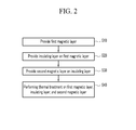
- FIG. 2 schematically shows a flowchart of a manufacturing method of the magnetic tunnel junction device 100 of FIG. 1 .
- the manufacturing method of the magnetic tunnel junction device 100 includes: i) providing the first magnetic layer 10 of FIG. 1 (S10); ii) providing the insulating layer 20 of FIG. 1 on the first magnetic layer 10 (S20); iii) providing the second magnetic layer 30 on the insulating layer 20 (S30); and thermally processing the first magnetic layer 10, the insulating layer 20, and the second magnetic layer 30 (S40).
- the manufacturing method of the magnetic tunnel junction device 100 may further include other steps.
- the first magnetic layer 10 is provided for manufacturing the magnetic tunnel junction device 100.
- the first magnetic layer 10 may be formed by a deposition method. If the ferromagnetic substance with an arranged crystal structure and a perpendicular magnetic anisotropy is used, deposition of the first magnetic layer 10 is performed by adding an amorphized element to the ferromagnetic substance. During the deposition process, the first magnetic layer 10 does not have perpendicular magnetic anisotropy. The first magnetic layer 10 has the perpendicular magnetic anisotropy by recovering a crystal structure through the thermal process of S40.
- a crystal lattice constant of the magnetic layer 10 may be greatly different from that of the insulating layer 20.
- the insulating layer 20 having a (001) orientation has difficulty in growth on the first magnetic layer 10.
- the flatness index of the insulating layer 20 is increased because the insulating layer 20 is greatly different from the first magnetic layer 10 in crystal lattice constant.
- a lattice constant of an alloy structured in the type of L1 0 having strong perpendicular magnetic anisotropy is greatly different from that of magnesium oxide which is used as a material of the insulating layer 20.
- magnesium oxide on the L1 0 -structure alloy it is difficult to grow magnesium oxide on the L1 0 -structure alloy to the (001) orientation of a crystal structure of B1. Furthermore, although magnesium oxide is grown on the L1 0 -sturcture alloy, the flatness index of the insulating layer 20 is increased due to a great difference in lattice constant therebetween, thereby causing a decrease of the regeneration signal value of the magnetic tunnel junction device 100.
- the first magnetic layer 10 according to the first exemplary embodiment of the present invention is amorphous so that the insulating layer 20 is grown well with the (001) orientation on the first magnetic 10.
- a crystal structure does not exist in the amorphous first magnetic layer 10.
- the first magnetic layer 10 and the insulating layer 20 do not have a crystal structure difference so that the flatness index of the insulating layer 20 is decreased. Accordingly, the regeneration signal value of the magnetic tunnel junction device 100 can be greatly increased and resistance of the magnetic tunnel junction device 100 can be greatly decreased.
- the insulating layer 20 is formed on the first magnetic layer 10. That is, the insulating layer 20 is deposed with the (001) orientation on the first magnetic layer 10. In addition, the flatness index of the insulating layer 20 is decreased.
- the second magnetic layer 30 is formed on the insulating layer 20.
- the second magnetic layer 30 is amorphous.
- the second magnetic layer 30 can be manufactured by using the same method as that of the first magnetic layer 10 of the step S10.
- FIG. 3 schematically shows a sequentially stacked first magnetic layer 10, insulating layer 20, and second magnetic layer 30 of the magnetic tunnel junction device before thermal treatment.
- the first and second magnetic layers 10 and 30 formed with the amorphous phase are not crystalline before the thermal treatment is performed on the magnetic tunnel junction device, the first and second magnetic layers 10 and 30 do not have perpendicular magnetic anisotropy.
- magnetized moments of the first and second magnetic layers 10 and 30 are formed along the x-axis direction, that is, the horizontal direction.
- the first magnetic layer 10, the insulating layer 20, and the second magnetic layer 30 manufactured through the above-described method are thermally treated in the step S40. While the first magnetic layer 10, the insulating layer 20, and the second magnetic layer 30 experience the thermal treatment at a high temperature for a sufficient period of time, the first and second magnetic layers 10 and 30 having the chemical formula of (A 100-x B x ) 100-y C y may be recovered to the arranged crystal structure. In further detail, the thermal treatment may be performed for several minutes to several hours at a temperature of 300°C to 600°C in order to prevent performance deterioration of the magnetic tunnel junction device due to diffusion of other elements.
- the first and second magnetic layers 10 and 30 changed to amorphous ferromagnetic substances by the thermal treatment gain perpendicular magnetic anisotropy while being changed to the arranged crystal structure. That is, the magnetic tunnel junction device is manufactured by respectively depositing the first and second magnetic layers 10 and 30 in the amorphous phase and then the magnetic tunnel junction device is thermally treated according to the first exemplary embodiment of the present invention.
- the regeneration signal value of the magnetic tunnel junction device 100 can be increased and thermal stability thereof can be increased with a small volume. Accordingly, perpendicular magnetic anisotropy of the magnetic tunnel junction device 100 can be assured while the first magnetic layer 10, the second magnetic layer 30, and the insulating layer 20 with materials having excellent signal characteristics are manufactured.
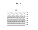
- FIG. 4 schematically shows a cross-sectional view of a magnetic tunnel junction device 200 according to a second exemplary embodiment of the present invention.
- the magnetic tunnel junction device 200 of FIG. 4 is similar to the magnetic tunnel junction device 100 of FIG. 1 , and therefore like reference numerals designate like elements and detailed description thereof will be omitted.
- the magnetic tunnel junction device 200 includes a first magnetic layer 10, an insulating layer 20, a second magnetic layer 30, horizontal anisotropic magnetic layers 40 and 42, and crystalline inductive layers 50 and 52.
- the horizontal anisotropic magnetic layers 40 and 42 are used to compensate a great difference in crystal structure between the magnetic layers 10 and 30 and the insulating layer 20.
- the horizontal anisotropic magnetic layers 40 and 42 may be used to increase a regeneration signal value of the magnetic tunnel junction device 200.
- the insulating layer 20 matches the horizontal anisotropic magnetic layers 40 and 42, and the first magnetic layer 10 and the second magnetic layer 30 match the crystalline inductive layers 50 and 52.
- the first and second magnetic layers 10 and 30 having vertical anisotropy do not match the horizontal anisotropic magnetic layers 40 and 42, but they are magnetically connected thereto. Accordingly, the strong vertical anisotropy of the first and second magnetic layers 10 and 30 vertically arrange magnetic moments of the horizontal anisotropic magnetic layers 40 and 42 so that a magnetic tunnel junction having perpendicular magnetic anisotropy can be realized in the magnetic tunnel junction device 200.
- the horizontal anisotropic magnetic layers 40 and 42 have a high spin polarization rate, and lattice constants thereof are slightly different from that of the insulating layer 20.
- the horizontal anisotropic magnetic layers 40 and 42 may be formed of a material such as Fe, CoFe, or CoFeB.
- the crystalline inductive layers 50 and 52 make the amorphous first and second magnetic layers 10 and 30 have an arranged crystal structure through thermal treatment without contacting the insulating layer 20.
- the first magnetic layer 10 and the second magnetic layer 30 are formed of FePdB or FePtB, Pd, Pt, Au, or Fe is grown to have a (100) orientation so as to be used as a material of the crystalline inductive layers 50 and 52.
- perpendicular magnetic anisotropy of the magnetic tunnel junction device 200 can be realized by using the horizontal anisotropic magnetic layers 40 and 42 and the crystalline inductive layers 50 and 52.
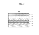
- FIG. 5 schematically shows a cross-sectional view of a magnetic tunnel junction device 300 according to a third exemplary embodiment of the present invention.
- the magnetic tunnel junction device 300 of FIG. 5 is similar to the magnetic tunnel junction device 200 of FIG. 4 , and therefore like reference numerals designate like elements and detailed description thereof will be omitted.
- the magnetic tunnel junction device 300 includes a first magnetic layer 10, an insulating layer 20, a horizontal anisotropic magnetic layer 40, a crystalline inductive layer 50, a horizontal anisotropic magnetic layer 60, and a perpendicular magnetic anisotropic inductive layer 62.
- a structure of the insulating layer 20 of the magnetic tunnel junction device 300 of FIG. 5 is the same as that of the magnetic tunnel junction device 200, excluding an upper structure thereof.
- the magnetic tunnel junction device 300 may use an amorphous material at one side and a crystalline material at the other end as a perpendicular magnetic anisotropic inductive layer. After thermal treatment, the amorphous material becomes the first magnetic layer 10 and the crystalline material becomes the perpendicular magnetic anisotropic inductive layer 62.
- an amorphous material is used as a perpendicular magnetic anisotropic inductive layer in a lower portion of the insulating layer 20.
- the lower structure of the insulating layer 20 is the same as that of the insulating layer 20 of the magnetic tunnel junction device of FIG. 4 .
- the horizontal anisotropic magnetic layer 50 and the crystalline perpendicular magnetic anisotropic inductive layer 62 are formed in an upper portion of the insulating layer 20 of the magnetic tunnel junction device 300.
- the horizontal anisotropic magnetic layer 50 may be formed of a CoFeB alloy
- the perpendicular magnetic anisotropic inductive layer 62 may be formed of a multi-layered Co/Pt alloy.
- a magnetic tunnel junction device was manufactured by sequentially stacking a magnetic layer, an insulating layer, and a magnetic layer.
- the magnetic layer was manufactured by adding 20at% of boron to a Fe 50 Pd 50 alloy having 1:1 element contents.
- the Fe 50 Pd 50 alloy had an arranged crystal structure and perpendicular magnetic anisotropy.
- the magnetic layer was amorphized by adding boron.
- the thickness of the magnetic layer was 3nm.
- the insulating layer was deposited on the magnetic layer.
- the insulating layer was formed of magnesium oxide, and had a thickness of 10nm.
- the magnetic layer formed of (Fe 50 Pd 50 ) 80 B 20 was deposited on the insulating layer.
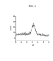
- FIG. 6 shows an X-ray diffraction graph of a magnetic tunnel junction device manufactured according to Experimental Example 1.
- the X-ray diffraction peak was observed at a location where 2 ⁇ is approximately 43°. This implies that MgO, that is, the insulating layer, was grown with a (001) orientation. Accordingly, it shows that the insulating layer was grown with a (001) orientation on the magnetic layer. In addition, since the insulating layer was deposited on the amorphized magnetic layer, it is predicted that the flatness index of the insulating layer would be low.
- a Pt layer was deposited at 40nm to have a (001) orientation on a single crystal substrate formed of MgO having a (001) orientation.
- the Pt layer had a thickness of 40nm, and functioned as a crystalline inductive layer of an amorphous magnetic layer.
- a magnetic layer formed of (Fe 50 Pd 50 ) 80 B 20 was deposited in the amorphous phase on the Pt layer.
- the thickness of the magnetic layer formed of (Fe 50 Pd 50 ) 80 B 20 was 10nm.
- the magnetic layer was deposited and thermal treatment was performed for one hour at 500 °C.
- FIG. 7 shows a magnetic hysteresis curve of a magnetic layer of a magnetic tunnel junction device manufactured according to the second experimental example before thermal treatment and after thermal treatment.
- the magnetic layer is formed of (Fe 50 Pd 50 ) 80 B 20 .
- the thin line indicates a degree of normal magnetization in the amorphous phase before thermal treatment
- the thick line indicates a degree of normal magnetization in the state that a crystal structure is recovered after thermal treatment.
- intensity of magnetization was increased in proportion to a magnetic field before the magnetic layer formed of (Fe 50 Pd 50 ) 80 B 20 is thermally treated, and the magnetization of the magnetic layer was saturated around 7000 Oe which is a value of a demagnetization field value generated from a shape deposited in a thin film state.
- a saturation magnetic moment of the magnetic layer formed of (Fe 50 Pd 50 ) 80 B 20 was 560emu/cc, and the demagnetization field value was 7000 Oe when the deposited shape was a thin film.
- the magnetic layer formed of (Fe 50 Pd 50 ) 80 B 20 does not have a crystal structure before the thermal treatment, the magnetic layer had horizontal magnetic anisotropy without assuring perpendicular magnetic anisotropy.
- the magnetization of the magnetic layer was saturated around 1000 Oe, which is smaller than 7000 Oe. That is, the perpendicular magnetic anisotropy was assured while a crystal structure of the magnetic layer formed of (Fe 50 Pd 50 ) 80 B 20 was recovered after the thermal treatment.
Landscapes
- Engineering & Computer Science (AREA)
- Power Engineering (AREA)
- Chemical & Material Sciences (AREA)
- Crystallography & Structural Chemistry (AREA)
- Manufacturing & Machinery (AREA)
- Nanotechnology (AREA)
- Physics & Mathematics (AREA)
- Computer Hardware Design (AREA)
- Spectroscopy & Molecular Physics (AREA)
- Condensed Matter Physics & Semiconductors (AREA)
- General Physics & Mathematics (AREA)
- Hall/Mr Elements (AREA)
- Mram Or Spin Memory Techniques (AREA)
- Thin Magnetic Films (AREA)
Abstract
Description
- The present invention relates to a magnetic tunnel junction device and a method for manufacturing the same. More particularly, it relates to a magnetic tunnel junction device using an amorphous perpendicular magnetic anisotropic material, and a method of manufacturing the same.
- Recently, various types of memories have been developed. For example, a magnetic random access memory (MRAM), a phase-change random access memory (PRAM), and a resistive random access memory (RRAM) have been developed.
- The MRAM uses a magnetic tunnel junction (MJT) element as a data storage element. The magnetic tunnel junction is included in a memory cell and thus forms a ferromagnetic tunnel junction. The magnetic tunnel junction element is structured with a magnetic layer, an insulating layer, and a magnetic layer, and a current flows in the insulating layer through the tunneling mechanism. Here, when relative magnetization directions of the two magnetic layers are equivalent to each other, the magnetic tunnel junction element has low resistance. On the contrary, when the two magnetic layers have different magnetization directions, the magnetic tunnel junction element has high resistance. The low resistance and the high resistance indicate digital data, respectively corresponding to 0 and 1.
- Thermal stability is defined as the ability of maintaining the digital data for a long period of time. The thermal stability is proportional to anisotropy energy of the magnetic layer of the magnetic tunnel junction element. Most anisotropy energy of a horizontal magnetic anisotropic ferromagnetic substance used as a material of the magnetic tunnel junction element is shape anisotropy energy, and therefore the entire anisotropy energy is small. In order to solve this problem, a perpendicular magnetic anisotropic ferromagnetic substance having high crystalline anisotropy energy is used as a material of the magnetic tunnel junction element. Accordingly, the entire anisotropy energy of the magnetic tunnel junction device is large so that the magnetic tunnel junction device can have superior thermal stability with a small volume.
- The above information disclosed in this Background section is only for enhancement of understanding of the background of the invention and therefore it may contain information that does not form the prior art that is already known in this country to a person of ordinary skill in the art.
- The present invention has been made in an effort to provide a magnetic tunnel junction device having advantages of increasing a regeneration signal value and improving thermal stability. In addition, the present invention provides a manufacturing method of the magnetic tunnel junction device.
- A magnetic tunnel junction device according to an exemplary embodiment of the present invention includes: i) a first magnetic layer including a compound having a chemical formula of (A100-xBx)100-yCy; ii) an insulating layer disposed on the first magnetic layer; and iii) a second magnetic layer disposed on the insulating layer and including a compound having a chemical formula of (A100-xBx)100-yCy. The first and second magnetic layers have perpendicular magnetic anisotropy, and A and B are metal elements and C is at least one amorphized element selected from a group consisting of boron (B), carbon (C), tantalum (Ta), and hafnium (Hf).
- A may be at least one element selected from a group consisting of iron (Fe), cobalt (Co), nickel (Ni), manganese (Mn), and chrome (Cr). B may be at least one element selected from a group consisting of platinum (Pt), palladium (Pd), rhodium (Rh), gold (Au), mercury (Hg), and aluminum (Al). The insulating layer includes a compound having a chemical formula of D100-zEz, and D may be at least one element selected from a group consisting of lithium (Li), beryllium (Be), sodium (Na), magnesium (Mg), niobium (Nb), titanium (Ti), vanadium (V), tantalum (Ta), barium (Ba), palladium (Pd), zirconium (Zr), holmium (Ho), potassium (K), and silver (Ag), and E is at least one element selected from a group consisting of oxygen (O), nitrogen (N), carbon (C), hydrogen (H), selenium (Se), chlorine (Cl), and fluorine (F). At least one of the first and second magnetic layers may have a cubic or tetragonal structure.
- The magnetic tunnel junction device according to the exemplary embodiment of the present invention may further include i) a first horizontal magnetic anisotropic magnetic layer disposed between the second magnetic layer and the insulating layer and ii) a first crystalline inductive layer disposed on the second magnetic layer. The first horizontal magnetic anisotropic magnetic layer may include at least one element selected from a group consisting of Fe, CoFe, and CoFeB. When the compound included at least one of the first and second magnetic layers has a chemical formula of (Fe100-xPdx)100-xBx or (Fe100-xPtx)100-xBx, the first crystalline inductive layer may include at least one element selected from a group consisting of Pd, Pt, Au, and Fe. The magnetic tunnel junction device according to the exemplary embodiment of the present invention may further include i) a second horizontal magnetic anisotropic magnetic layer disposed between the first magnetic layer and the insulating layer and ii) a second crystalline inductive layer disposed under the first magnetic layer.
- A magnetic tunnel junction device according to another exemplary embodiment of the present invention includes: i) a crystalline inductive layer; ii) a perpendicular magnetic anisotropic magnetic layer disposed on the crystalline inductive layer and including a compound having a chemical formula of (A100-xBx)100-yCy; iii) a horizontal magnetic anisotropic magnetic layer disposed on the perpendicular magnetic anisotropic magnetic layer; iv) an insulating layer disposed on the horizontal magnetic anisotropic magnetic layer; v) a horizontal magnetic anisotropic inductive layer disposed on the insulating layer; and vi) a perpendicular magnetic anisotropic magnetic layer disposed on the horizontal magnetic anisotropic magnetic layer. A may be at least one element selected from a group consisting of iron (Fe), cobalt (Co), nickel (Ni), manganese (Mn), and chrome (Cr), B is at least one element selected from a group consisting of platinum (Pt), palladium (Pd), rhodium (Rh), gold (Au), mercury (Hg), and aluminum (Al), and C is at least one element selected from a group consisting of boron (B), carbon (C), tantalum (Ta), and hafnium (Hf).
- A manufacturing method of a magnetic tunnel junction device according to another exemplary embodiment of the present invention includes: i) providing a first magnetic layer including an amorphized element; ii) providing an insulating layer on the first magnetic layer; iii) providing a second magnetic layer including an amorphized element on the insulating layer; and iv) crystallizing the first and second magnetic layers by performing thermal treatment on the first magnetic layer, the insulating layer, and the second magnetic layer.
- In the providing of the first magnetic layer and in the providing of the second magnetic layer, the first and second magnetic layers may respectively include a compound having a chemical formula of (A100-xBx)100-yCy, and A may be at least one element selected from a consisting of iron (Fe), cobalt (Co), nickel (Ni), manganese (Mn), and chrome (Cr), B may be at least one element selected from a group consisting of platinum (Pt), palladium (Pd), rhodium (Rh), gold (Au), mercury (Hg), and aluminum (Al), and C may be at least one amorphized element selected from a group consisting of boron (B), carbon (C), tantalum (Ta), and hafnium (Hf). In the crystallizing of the first and second magnetic layers, the first and second magnetic layers may have perpendicular magnetic anisotropy. In the crystallizing of the first and second magnetic layers, the thermal treatment may be performed on the first magnetic layer, the insulating layer, and the second magnetic layer at 300°C to 600°C.
- The manufacturing method according to the other exemplary embodiment of the present invention may further include i) providing a horizontal magnetic anisotropic magnetic layer between the second magnetic layer and the insulating layer and ii) providing a crystalline inductive layer on the second magnetic layer. The manufacturing method according to the other exemplary embodiment of the present invention may further include i) providing another horizontal magnetic anisotropic magnetic layer between the first magnetic layer and the insulating layer and ii) providing a crystalline inductive layer under the first magnetic layer.
- A manufacturing method of a magnetic tunnel junction device according to another exemplary embodiment of the present invention includes: i) providing a crystalline inductive layer; ii) providing a magnetic layer including a compound having a chemical formula of (A100-xBx)100-yCy on the crystalline inductive layer; iii) providing a first horizontal magnetic anisotropic magnetic layer on the magnetic layer; iv) providing an insulating layer on the first horizontal magnetic anisotropic magnetic layer; v) providing a second horizontal magnetic anisotropic magnetic layer on the insulating layer; vi) providing a perpendicular magnetic anisotropic magnetic layer on the second horizontal magnetic anisotropic magnetic layer; and vii) crystallizing the magnetic layer by performing thermal treatment on the crystalline inductive layer, the magnetic layer, the first horizontal magnetic anisotropic magnetic layer, the insulating layer, the second horizontal magnetic anisotropic magnetic layer, and the perpendicular magnetic anisotropic magnetic layer,
- In the crystallizing of the magnetic layer, the magnetic layer may have perpendicular magnetic anisotropy and may include a compound having a chemical formula of (A100-xBx)100-yCy in which A may be at least one element selected from a group consisting of iron (Fe), cobalt (Co), nickel (Ni), manganese (Mn), and chrome (Cr), B may be at least one element selected from a group consisting of platinum (Pt), palladium (Pd), rhodium (Rh), gold (Au), mercury (Hg), and aluminum (Al), and C may be at least one amorphized element selected from a group consisting of boron (B), carbon (C), tantalum (Ta), and hafnium (Hf).
- According to the present invention, the insulating layer is deposited on the amorphous magnetic layer so that the insulating layer is deposited with low flatness index. Accordingly, the magnetic tunnel junction device having a high regeneration signal value can be manufactured. In addition, a crystal structure of the amorphous magnetic layer is recovered through thermal treatment so that it has perpendicular magnetic anisotropy. Accordingly, the magnetic tunnel junction device having higher thermal stability can be manufactured. As a result, the regeneration signal value and thermal stability of the magnetic tunnel junction device can be increased so that the magnetic tunnel junction device can be used in a magnetic random access memory (MRAM) or a high frequency oscillator.
-
-
FIG. 1 schematically shows a cross-sectional view of a magnetic tunnel junction device according to a first exemplary embodiment of the present invention. -
FIG. 2 schematically shows a flowchart of a manufacturing method of the magnetic tunnel junction device ofFIG. 1 . -
FIG. 3 schematically shows a magnetic tunnel junction device formed of a sequentially stacked first magnetic layer, insulating layer, and second magnetic layer before thermal treatment. -
FIG. 4 schematically shows a cross-sectional view of a magnetic tunnel junction device according to a second exemplary embodiment of the present invention. -
FIG. 5 schematically shows a cross-sectional view of a magnetic tunnel junction device according to a third exemplary embodiment of the present invention. -
FIG. 6 is an X-ray diffraction graph of a magnetic tunnel junction device manufactured according to a first experimental example. -
FIG. 7 is a magnetic hysteresis curve of a magnetic layer of a magnetic tunnel junction device manufactured according to a second experimental example before thermal treatment and after thermal treatment. - It will be understood that when an element is referred to as being "on" another element, it can be directly on another element or intervening elements may be present therebetween. In contrast, when an element is referred to as being "directly on" another element, there are no intervening elements therebetween.
- It will be understood that, although the terms first, second, third, etc. may be used herein to describe various elements, components, regions, layers, and/or sections, they are not limited thereto. These terms are only used to distinguish one element, component, region, layer, or section from another element, component, region, layer, or section. Thus, a first element, component, region, layer, or section discussed below could be termed a second element, component, region, layer, or section without departing from the teachings of the present invention.
- Terminologies used herein are provided to merely mention specific exemplary embodiments and are not intended to limit the present invention. Singular expressions used herein include plurals unless they have definitely opposite meanings. The meaning of "including" used in this specification gives shape to specific characteristics, regions, positive numbers, steps, operations, elements, and/or components, and do not exclude the existence or addition of other specific characteristics, regions, positive numbers, steps, operations, elements, components, and/or groups.
- Spatially relative terms, such as "below" and "above" and the like, may be used herein for ease of description to describe one element or feature's relationship to another element(s) or feature(s) as illustrated in the figures. It will be understood that spatially relative terms are intended to encompass different orientations of the device in use or operation in addition to the orientation depicted in the drawings. For example, if the device in the figures is turned over, elements described as "below" other elements or features would then be oriented "above" the other elements or features. Thus, the exemplary term "below" can encompass both an orientation of above and below. Apparatuses may be otherwise rotated 90 degrees or at other angles, and the spatially relative descriptors used herein are then interpreted accordingly.
- All the terminologies including technical terms and scientific terms used herein have the same meanings that those skilled in the art generally understandTerms defined in dictionaries are construed to have meanings corresponding to related technical documents and the present description, and they are not construed as ideal or very official meanings, if not defined.
- Exemplary embodiments of the present invention described with reference to cross-sectional views represent ideal exemplary embodiments of the present invention in detail. Therefore, various modification of diagrams, for example, modifications of manufacturing methods and/or specifications, are expected. Accordingly, exemplary embodiments are not limited to specific shapes of shown regions, and for example, also include modifications of the shape by manufacturing. For example, regions shown or described as flat may generally have rough or rough and nonlinear characteristics. Further, portions shown to have sharp angles may be rounded. Therefore, the regions shown in the drawings are basically just schematic and the shapes thereof are not intended to show the exact shapes of the region and are also not intended to reduce the scope of the present invention.
- In the specification, the term "flatness index" implies an index indicating height deviation of thin film interface in a perpendicular direction. If the flatness index is low, the height of interface is constant, that is, the interface is flat. On the contrary, if the flatness index is high, the height deviation of interface is great, that is, the interface is curved. In order to increase a regeneration signal of an element, it is preferably to form a flat interface by decreasing the flatness index of an insulating layer.
-
FIG. 1 schematically shows a cross-sectional structure of a magnetictunnel junction device 100 according to a first exemplary embodiment of the present invention. The cross-sectional structure of the magnetictunnel junction device 100 shown inFIG. 1 is an example of the present invention, and the present invention is not limited thereto. That is, the cross-sectional structure of the magnetictunnel junction device 100 can be modified in various shapes. - As shown in
FIG. 1 , the magnetictunnel junction device 100 includes a firstmagnetic layer 10, an insulatinglayer 20, and a secondmagnetic layer 30. The firstmagnetic layer 10 functions as a fixed magnetic layer, and the secondmagnetic layer 30 functions as a free magnetic layer. In order to increase thermal stability of the magnetictunnel junction device 100, the first and secondmagnetic layers - The first
magnetic layer 10 and the secondmagnetic layer 30 respectively include a material having a chemical formula of (A100-xBx)100-yCy. Here, A and B may respectively be metal elements. In further detail, A may be iron (Fe), cobalt (Co), nickel (Ni), manganese (Mn), or chrome (Cr). In addition, B may be platinum (Pt), palladium (Pd), rhodium (Rh), gold (Au), mercury (Hg), or aluminum (Al). Further, C may be boron (B), carbon (C), tantalum (Ta), and hafnium (Hf). - An alloy having a chemical formula of A100-xBx has an arranged structured. The arranged structure may be a cubic structure or a tetragonal structure. The cubic structure may exemplarily include a crystal structure of an L12 type. In addition, the tetragon structure may exemplarily include a crystal structure of L10. C is an alloy having a chemical formula of A100-xBx before thermal treatment for amorphization. The first
magnetic layer 10 and the secondmagnetic layer 30 may be respectively formed of different materials or the same material. - The insulating
layer 20 includes a compound having a chemical formula of D100-zEz. Here, D is at least one element selected from a group consisting of lithium (Li), beryllium (Be), sodium (Na), magnesium (Mg), niobium (Nb), titanium (Ti), vanadium (V), tantalum (Ta), barium (Ba), palladium (Pd), zirconium (Zr), holmium (Ho), potassium (K), and silver (Ag), and E is at least one element selected from a group consisting of oxygen (O), nitrogen (N), carbon (C), hydrogen (H), selenium (Se), chlorine (Cl), and fluorine (F). For example, the insulatinglayer 20 may be made of magnesium oxide (MgO). - The insulating
layer 20 may have a cubic structure. The cubic structure may exemplarily include a crystal structure of a B1 type. The insulating layer may have a (001) orientation along a direction that is perpendicular to a substrate surface of a thin film interface for increasing a regeneration signal value of the magnetictunnel junction device 100. - As shown by the arrow of
FIG. 1 , the firstmagnetic layer 10 and the secondmagnetic layer 30 have perpendicular magnetic anisotropy after recovering their crystal structures through thermal treatment. Accordingly, the magnetictunnel junction device 100 having excellent thermal stability and a high regeneration signal value can be manufactured. Hereinafter, a manufacturing method of the magnetictunnel junction device 100 ofFIG. 1 will be described in further detail with reference toFIG. 2 andFIG. 3 . -
FIG. 2 schematically shows a flowchart of a manufacturing method of the magnetictunnel junction device 100 ofFIG. 1 . - As shown in
FIG. 2 , the manufacturing method of the magnetictunnel junction device 100 includes: i) providing the firstmagnetic layer 10 ofFIG. 1 (S10); ii) providing the insulatinglayer 20 ofFIG. 1 on the first magnetic layer 10 (S20); iii) providing the secondmagnetic layer 30 on the insulating layer 20 (S30); and thermally processing the firstmagnetic layer 10, the insulatinglayer 20, and the second magnetic layer 30 (S40). The manufacturing method of the magnetictunnel junction device 100 may further include other steps. - In the step S10, the first
magnetic layer 10 is provided for manufacturing the magnetictunnel junction device 100. The firstmagnetic layer 10 may be formed by a deposition method. If the ferromagnetic substance with an arranged crystal structure and a perpendicular magnetic anisotropy is used, deposition of the firstmagnetic layer 10 is performed by adding an amorphized element to the ferromagnetic substance. During the deposition process, the firstmagnetic layer 10 does not have perpendicular magnetic anisotropy. The firstmagnetic layer 10 has the perpendicular magnetic anisotropy by recovering a crystal structure through the thermal process of S40. - In the case that the first
magnetic layer 10 has a crystal structure, a crystal lattice constant of themagnetic layer 10 may be greatly different from that of the insulatinglayer 20. In this case, the insulatinglayer 20 having a (001) orientation has difficulty in growth on the firstmagnetic layer 10. In addition, although the insulatinglayer 20 having the (001) orientation grows on the insulatinglayer 20, the flatness index of the insulatinglayer 20 is increased because the insulatinglayer 20 is greatly different from the firstmagnetic layer 10 in crystal lattice constant. Particularly, a lattice constant of an alloy structured in the type of L10 having strong perpendicular magnetic anisotropy is greatly different from that of magnesium oxide which is used as a material of the insulatinglayer 20. Therefore, it is difficult to grow magnesium oxide on the L10-structure alloy to the (001) orientation of a crystal structure of B1. Furthermore, although magnesium oxide is grown on the L10-sturcture alloy, the flatness index of the insulatinglayer 20 is increased due to a great difference in lattice constant therebetween, thereby causing a decrease of the regeneration signal value of the magnetictunnel junction device 100. - However, the first
magnetic layer 10 according to the first exemplary embodiment of the present invention is amorphous so that the insulatinglayer 20 is grown well with the (001) orientation on the first magnetic 10. In addition, a crystal structure does not exist in the amorphous firstmagnetic layer 10. Thus, the firstmagnetic layer 10 and the insulatinglayer 20 do not have a crystal structure difference so that the flatness index of the insulatinglayer 20 is decreased. Accordingly, the regeneration signal value of the magnetictunnel junction device 100 can be greatly increased and resistance of the magnetictunnel junction device 100 can be greatly decreased. - In the step S20, the insulating
layer 20 is formed on the firstmagnetic layer 10. That is, the insulatinglayer 20 is deposed with the (001) orientation on the firstmagnetic layer 10. In addition, the flatness index of the insulatinglayer 20 is decreased. - In the step S30, the second
magnetic layer 30 is formed on the insulatinglayer 20. The secondmagnetic layer 30 is amorphous. The secondmagnetic layer 30 can be manufactured by using the same method as that of the firstmagnetic layer 10 of the step S10. -
FIG. 3 schematically shows a sequentially stacked firstmagnetic layer 10, insulatinglayer 20, and secondmagnetic layer 30 of the magnetic tunnel junction device before thermal treatment. - Since the first
magnetic layer 10 and the secondmagnetic layer 30 formed with the amorphous phase are not crystalline before the thermal treatment is performed on the magnetic tunnel junction device, the first and secondmagnetic layers FIG. 3 , magnetized moments of the first and secondmagnetic layers - Referring back to
FIG. 2 , the firstmagnetic layer 10, the insulatinglayer 20, and the secondmagnetic layer 30 manufactured through the above-described method are thermally treated in the step S40. While the firstmagnetic layer 10, the insulatinglayer 20, and the secondmagnetic layer 30 experience the thermal treatment at a high temperature for a sufficient period of time, the first and secondmagnetic layers - The first and second
magnetic layers magnetic layers magnetic layers tunnel junction device 100 can be increased and thermal stability thereof can be increased with a small volume. Accordingly, perpendicular magnetic anisotropy of the magnetictunnel junction device 100 can be assured while the firstmagnetic layer 10, the secondmagnetic layer 30, and the insulatinglayer 20 with materials having excellent signal characteristics are manufactured. -
FIG. 4 schematically shows a cross-sectional view of a magnetictunnel junction device 200 according to a second exemplary embodiment of the present invention. The magnetictunnel junction device 200 ofFIG. 4 is similar to the magnetictunnel junction device 100 ofFIG. 1 , and therefore like reference numerals designate like elements and detailed description thereof will be omitted. - As shown in
FIG. 4 , the magnetictunnel junction device 200 includes a firstmagnetic layer 10, an insulatinglayer 20, a secondmagnetic layer 30, horizontal anisotropicmagnetic layers inductive layers magnetic layers magnetic layers layer 20. In addition, the horizontal anisotropicmagnetic layers tunnel junction device 200. - In this case, the insulating
layer 20 matches the horizontal anisotropicmagnetic layers magnetic layer 10 and the secondmagnetic layer 30 match the crystallineinductive layers magnetic layers magnetic layers magnetic layers magnetic layers tunnel junction device 200. - The horizontal anisotropic
magnetic layers layer 20. The horizontal anisotropicmagnetic layers - Meanwhile, the crystalline
inductive layers magnetic layers layer 20. For example, when the firstmagnetic layer 10 and the secondmagnetic layer 30 are formed of FePdB or FePtB, Pd, Pt, Au, or Fe is grown to have a (100) orientation so as to be used as a material of the crystallineinductive layers - As described above, although the first and second
magnetic layers layer 20 are greatly different from each other in crystal structure, perpendicular magnetic anisotropy of the magnetictunnel junction device 200 can be realized by using the horizontal anisotropicmagnetic layers inductive layers -
FIG. 5 schematically shows a cross-sectional view of a magnetictunnel junction device 300 according to a third exemplary embodiment of the present invention. The magnetictunnel junction device 300 ofFIG. 5 is similar to the magnetictunnel junction device 200 ofFIG. 4 , and therefore like reference numerals designate like elements and detailed description thereof will be omitted. - As shown in
FIG. 5 , the magnetictunnel junction device 300 includes a firstmagnetic layer 10, an insulatinglayer 20, a horizontal anisotropicmagnetic layer 40, a crystallineinductive layer 50, a horizontal anisotropicmagnetic layer 60, and a perpendicular magnetic anisotropicinductive layer 62. - A structure of the insulating
layer 20 of the magnetictunnel junction device 300 ofFIG. 5 is the same as that of the magnetictunnel junction device 200, excluding an upper structure thereof. - As shown in
FIG. 5 , the magnetictunnel junction device 300 may use an amorphous material at one side and a crystalline material at the other end as a perpendicular magnetic anisotropic inductive layer. After thermal treatment, the amorphous material becomes the firstmagnetic layer 10 and the crystalline material becomes the perpendicular magnetic anisotropicinductive layer 62. InFIG. 5 , an amorphous material is used as a perpendicular magnetic anisotropic inductive layer in a lower portion of the insulatinglayer 20. In this case, the lower structure of the insulatinglayer 20 is the same as that of the insulatinglayer 20 of the magnetic tunnel junction device ofFIG. 4 . - As shown in
FIG. 5 , the horizontal anisotropicmagnetic layer 50 and the crystalline perpendicular magnetic anisotropicinductive layer 62 are formed in an upper portion of the insulatinglayer 20 of the magnetictunnel junction device 300. For example, the horizontal anisotropicmagnetic layer 50 may be formed of a CoFeB alloy, and the perpendicular magnetic anisotropicinductive layer 62 may be formed of a multi-layered Co/Pt alloy. - Hereinafter, the present invention will be described in further detail through experimental examples. The experimental examples are provided as examples of the present invention, and therefore the present invention is not limited thereto.
- A magnetic tunnel junction device was manufactured by sequentially stacking a magnetic layer, an insulating layer, and a magnetic layer. The magnetic layer was manufactured by adding 20at% of boron to a Fe50Pd50 alloy having 1:1 element contents. The Fe50Pd50 alloy had an arranged crystal structure and perpendicular magnetic anisotropy. The magnetic layer was amorphized by adding boron. The thickness of the magnetic layer was 3nm.
- Next, the insulating layer was deposited on the magnetic layer. The insulating layer was formed of magnesium oxide, and had a thickness of 10nm. The magnetic layer formed of (Fe50Pd50)80B20 was deposited on the insulating layer.
-
FIG. 6 shows an X-ray diffraction graph of a magnetic tunnel junction device manufactured according to Experimental Example 1. - As shown in
FIG. 6 , the X-ray diffraction peak was observed at a location where 2θ is approximately 43°. This implies that MgO, that is, the insulating layer, was grown with a (001) orientation. Accordingly, it shows that the insulating layer was grown with a (001) orientation on the magnetic layer. In addition, since the insulating layer was deposited on the amorphized magnetic layer, it is predicted that the flatness index of the insulating layer would be low. - A Pt layer was deposited at 40nm to have a (001) orientation on a single crystal substrate formed of MgO having a (001) orientation. Here, the Pt layer had a thickness of 40nm, and functioned as a crystalline inductive layer of an amorphous magnetic layer. Next, a magnetic layer formed of (Fe50Pd50)80B20 was deposited in the amorphous phase on the Pt layer. The thickness of the magnetic layer formed of (Fe50Pd50)80B20 was 10nm. The magnetic layer was deposited and thermal treatment was performed for one hour at 500 °C.
-
FIG. 7 shows a magnetic hysteresis curve of a magnetic layer of a magnetic tunnel junction device manufactured according to the second experimental example before thermal treatment and after thermal treatment. Here, the magnetic layer is formed of (Fe50Pd50)80B20. InFIG. 7 , the thin line indicates a degree of normal magnetization in the amorphous phase before thermal treatment, and the thick line indicates a degree of normal magnetization in the state that a crystal structure is recovered after thermal treatment. - As shown in
FIG. 7 , intensity of magnetization was increased in proportion to a magnetic field before the magnetic layer formed of (Fe50Pd50)80B20 is thermally treated, and the magnetization of the magnetic layer was saturated around 7000 Oe which is a value of a demagnetization field value generated from a shape deposited in a thin film state. A saturation magnetic moment of the magnetic layer formed of (Fe50Pd50)80B20 was 560emu/cc, and the demagnetization field value was 7000 Oe when the deposited shape was a thin film. That is, since the magnetic layer formed of (Fe50Pd50)80B20 does not have a crystal structure before the thermal treatment, the magnetic layer had horizontal magnetic anisotropy without assuring perpendicular magnetic anisotropy. However, after the magnetic layer formed of (Fe50Pd50)80B20 is thermally treated, the magnetization of the magnetic layer was saturated around 1000 Oe, which is smaller than 7000 Oe. That is, the perpendicular magnetic anisotropy was assured while a crystal structure of the magnetic layer formed of (Fe50Pd50)80B20 was recovered after the thermal treatment. - While this invention has been described in connection with what is presently considered to be practical exemplary embodiments, it is to be understood that the invention is not limited to the disclosed embodiments, but, on the contrary, is intended to cover various modifications and equivalent arrangements included within the spirit and scope of the appended claims.
Claims (17)
- A magnetic tunnel junction device (100) comprising:a first magnetic layer (10) including a compound having a chemical formula of (A100-xBx)100-yCy;an insulating layer (20) disposed on the first magnetic layer; anda second magnetic layer (30) disposed on the insulating layer (20) and including a compound having a chemical formula of (A100-xBx)100-yCy,wherein the first and second magnetic layers (10, 30) have perpendicular magnetic anisotropy, andA and B are metal elements and C is at least one amorphized element selected from a group consisting of boron (B), carbon (C), tantalum (Ta), and hafnium (Hf).
- The magnetic tunnel junction device (100) of claim 1, wherein A is at least one element selected from a group consisting of iron (Fe), cobalt (Co), nickel (Ni), manganese (Mn), and chrome (Cr).
- The magnetic tunnel junction device (100) of claim 2, wherein B is at least one element selected from a group consisting of platinum (Pt), palladium (Pd), rhodium (Rh), gold (Au), mercury (Hg), and aluminum (Al).
- The magnetic tunnel junction device (100) of claim 1, wherein the insulating layer (20) includes a compound having a chemical formula of D100-zEz, and D is at least one element selected from a group consisting of lithium (Li), beryllium (Be), sodium (Na), magnesium (Mg), niobium (Nb), titanium (Ti), vanadium (V), tantalum (Ta), barium (Ba), palladium (Pd), zirconium (Zr), holmium (Ho), potassium (K), and silver (Ag), and E is at least one element selected from a group consisting of oxygen (O), nitrogen (N), carbon (C), hydrogen (H), selenium (Se), chlorine (Cl), and fluorine (F).
- The magnetic tunnel junction device (100) of claim 1, wherein at least one of the first and second magnetic layers (10, 30) has a cubic or tetragonal structure.
- The magnetic tunnel junction device (200) of claim 1, further comprising:a first horizontal magnetic anisotropic magnetic layer (40) disposed between the second magnetic layer (30) and the insulating layer (20); anda first crystalline inductive layer (50) disposed on the second magnetic layer (30).
- The magnetic tunnel junction device (200) of claim 6, wherein the first horizontal magnetic anisotropic magnetic layer (40) comprises at least one element selected from a group consisting of Fe, CoFe, and CoFeB.
- The magnetic tunnel junction device (200) of claim 6, wherein when the compound included at least one of the first and second magnetic layers (10, 30) has a chemical formula of (Fe100-xPdx)100-xBx or (Fe100-xPtx)100-xBx, the first crystalline inductive layer (50) includes at least one element selected from a group consisting of Pd, Pt, Au, and Fe.
- The magnetic tunnel junction device (200) of claim 6, further comprising:a second horizontal magnetic anisotropic magnetic layer (42) disposed between the first magnetic layer (10) and the insulating layer (20); anda second crystalline inductive layer (52) disposed under the first magnetic layer (10).
- A magnetic tunnel junction device (300) comprising:a crystalline inductive layer (50);a perpendicular magnetic anisotropic magnetic layer (10) disposed on the crystalline inductive layer (50) and including a compound having a chemical formula of (A100-xBx)100-yCy;a horizontal magnetic anisotropic magnetic layer (40) disposed on the perpendicular magnetic anisotropic magnetic layer (10);an insulating layer (20) disposed on the horizontal magnetic anisotropic magnetic layer (40);a horizontal magnetic anisotropic magnetic layer (60) disposed on the insulating layer (20); anda perpendicular magnetic inductive magnetic layer (62) disposed on the horizontal magnetic anisotropic magnetic layer (60),wherein A is at least one element selected from a group consisting of iron (Fe), cobalt (Co), nickel (Ni), manganese (Mn), and chrome (Cr), B is at least one element selected from a group consisting of platinum (Pt), palladium (Pd), rhodium (Rh), gold (Au), mercury (Hg), and aluminum (Al), and C is at least one element selected from a group consisting of boron (B), carbon (C), tantalum (Ta), and hafnium (Hf).
- A manufacturing method of a magnetic tunnel junction device (100), comprising:providing a first magnetic layer (10) including an amorphized element;providing an insulating layer (20) on the first magnetic layer (10);providing a second magnetic layer (30) including an amorphized element on the insulating layer (20); andcrystallizing the first and second magnetic layers (10, 30) by performing thermal treatment on the first magnetic layer (10), the insulating layer (20), and the second magnetic layer (30).
- The manufacturing method of claim 11, wherein in the providing of the first magnetic layer (10) and in the providing of the second magnetic layer (30), the first and second magnetic layers (10, 30) respectively include a compound having a chemical formula of (A100-xBx)100-yCy, and A is at least one element selected from a consisting of iron (Fe), cobalt (Co), nickel (Ni), manganese (Mn), and chrome (Cr), B is at least one element selected from a group consisting of platinum (Pt), palladium (Pd), rhodium (Rh), gold (Au), mercury (Hg), and aluminum (Al), and C is at least one amorphized element selected from a group consisting of boron (B), carbon (C), tantalum (Ta), and hafnium (Hf).
- The manufacturing method of claim 11, wherein in the crystallizing of the first and second magnetic layers (10, 30), the first and second magnetic layers (10, 30) have perpendicular magnetic anisotropy.
- The manufacturing method of claim 11, wherein in the crystallizing of the first and second magnetic layers (10, 30), the thermal treatment is performed on the first magnetic layer (10), the insulating layer (20), and the second magnetic layer (30) at 300°C to 600°C.
- The manufacturing method of claim 11, further comprising:providing a horizontal magnetic anisotropic magnetic layer (40) between the second magnetic layer (30) and the insulating layer (20); andproviding a crystalline inductive layer (50) on the second magnetic layer (30).
- The manufacturing method of claim 15, further comprising:providing another horizontal magnetic anisotropic magnetic layer (42) between the first magnetic layer (10) and the insulating layer (20); andproviding a crystalline inductive layer (52) under the first magnetic layer (10).
- A manufacturing method of a magnetic tunnel junction device, comprising:providing a crystalline inductive layer (50);providing a magnetic layer (10) including a compound having a chemical formula of (A100-xBx)100-yCy on the crystalline inductive layer (50);providing a first horizontal magnetic anisotropic magnetic layer (40) on the magnetic layer (10);providing an insulating layer (20) on the first horizontal magnetic anisotropic magnetic layer (40);providing a second horizontal magnetic anisotropic magnetic layer (60) on the insulating layer (20);providing a perpendicular magnetic anisotropic magnetic layer (62) on the second horizontal magnetic anisotropic magnetic layer (60); andcrystallizing the magnetic layer (10) by performing thermal treatment on the crystalline inductive layer (50), the magnetic layer (10), the first horizontal magnetic anisotropic magnetic layer (40), the insulating layer (20), the second horizontal magnetic anisotropic magnetic layer (60), and the perpendicular magnetic anisotropic magnetic layer (62),wherein, in the crystallizing of the magnetic layer (10), the magnetic layer (10) has perpendicular magnetic anisotropy and includes a compound having a chemical formula of (A100-xBx)100-yCy in which A is at least one element selected from a group consisting of iron (Fe), cobalt (Co), nickel (Ni), manganese (Mn), and chrome (Cr), B is at least one element selected from a
group consisting of platinum (Pt), palladium (Pd), rhodium (Rh), gold (Au), mercury (Hg), and aluminum (Al), and C is at least one amorphized element selected from a group consisting of boron (B), carbon (C), tantalum (Ta), and hafnium (Hf).
Applications Claiming Priority (1)
| Application Number | Priority Date | Filing Date | Title |
|---|---|---|---|
| KR1020090077492A KR101115039B1 (en) | 2009-08-21 | 2009-08-21 | Magnetic tunnel junction device and method for manufacturing the same |
Publications (2)
| Publication Number | Publication Date |
|---|---|
| EP2287863A1 true EP2287863A1 (en) | 2011-02-23 |
| EP2287863B1 EP2287863B1 (en) | 2017-11-15 |
Family
ID=42245996
Family Applications (1)
| Application Number | Title | Priority Date | Filing Date |
|---|---|---|---|
| EP10162168.8A Not-in-force EP2287863B1 (en) | 2009-08-21 | 2010-05-06 | Magnetic tunnel junction device and method for manufacturing the same |
Country Status (4)
| Country | Link |
|---|---|
| US (2) | US8841006B2 (en) |
| EP (1) | EP2287863B1 (en) |
| JP (1) | JP5300701B2 (en) |
| KR (1) | KR101115039B1 (en) |
Cited By (1)
| Publication number | Priority date | Publication date | Assignee | Title |
|---|---|---|---|---|
| EP2595164A1 (en) * | 2011-11-18 | 2013-05-22 | Korea Institute of Science and Technology | Perpendicularly magnetized thin film structure and method for manufacturing the same |
Families Citing this family (18)
| Publication number | Priority date | Publication date | Assignee | Title |
|---|---|---|---|---|
| KR101115039B1 (en) * | 2009-08-21 | 2012-03-07 | 한국과학기술연구원 | Magnetic tunnel junction device and method for manufacturing the same |
| JP5725735B2 (en) * | 2010-06-04 | 2015-05-27 | 株式会社日立製作所 | Magnetoresistive element and magnetic memory |
| JP2012204432A (en) * | 2011-03-24 | 2012-10-22 | Toshiba Corp | Magnetic random access memory and manufacturing method thereof |
| US8817426B2 (en) | 2011-10-17 | 2014-08-26 | HGST Netherlands B.V. | Magnetic sensor having CoFeBTa in pinned and free layer structures |
| KR101901323B1 (en) | 2011-12-21 | 2018-09-27 | 삼성전자주식회사 | Magnetoresistive element and memory device including the same |
| US9490054B2 (en) * | 2012-10-11 | 2016-11-08 | Headway Technologies, Inc. | Seed layer for multilayer magnetic materials |
| KR101537449B1 (en) * | 2013-10-10 | 2015-07-16 | 한양대학교 산학협력단 | Method of manufacturing multilayer thin film and magnetic tunnel junction structure including the multilayer thin film |
| US9831422B2 (en) * | 2015-10-21 | 2017-11-28 | Samsung Electronics Co., Ltd. | Magnetic memory devices having perpendicular magnetic tunnel junction |
| US10115892B2 (en) | 2015-11-23 | 2018-10-30 | Headway Technologies, Inc. | Multilayer structure for reducing film roughness in magnetic devices |
| US9780299B2 (en) | 2015-11-23 | 2017-10-03 | Headway Technologies, Inc. | Multilayer structure for reducing film roughness in magnetic devices |
| US9966528B2 (en) * | 2016-03-07 | 2018-05-08 | Samsung Electronics Co., Ltd. | Method and system for providing a magnetic layer in a magnetic junction usable in spin transfer torque applications using a sacrificial oxide layer |
| US10438638B2 (en) * | 2016-03-07 | 2019-10-08 | Samsung Electronics Co., Ltd. | Method and system for providing a magnetic layer in a magnetic junction usable in spin transfer or spin orbit torque applications using a sacrificial oxide layer |
| US10490732B2 (en) | 2016-03-11 | 2019-11-26 | Toshiba Memory Corporation | Magnetic memory device with sidewall layer containing boron and manufacturing method thereof |
| TWI688131B (en) | 2016-09-14 | 2020-03-11 | 日商東芝記憶體股份有限公司 | Semiconductor device |
| US10283246B1 (en) | 2017-10-20 | 2019-05-07 | Globalfoundries Singapore Pte. Ltd. | MTJ structures, STT MRAM structures, and methods for fabricating integrated circuits including the same |
| CN108062450B (en) * | 2018-01-03 | 2021-03-16 | 中国铁路设计集团有限公司 | Design method of ground settlement severe area in high-speed rail tunnel crossing area |
| CN112962122B (en) * | 2021-02-01 | 2022-03-15 | 浙江工业大学 | A kind of preparation method of high coercivity B-doped FePt thin film |
| CN114002252B (en) * | 2021-12-31 | 2022-04-26 | 季华实验室 | Detection method for perpendicular magnetic anisotropy of multilayer thin film materials |
Citations (4)
| Publication number | Priority date | Publication date | Assignee | Title |
|---|---|---|---|---|
| US20070086121A1 (en) * | 2005-10-19 | 2007-04-19 | Toshihiko Nagase | Magnetoresistive element |
| US20080088980A1 (en) * | 2006-10-13 | 2008-04-17 | Eiji Kitagawa | Magnetoresistive element and magnetic memory |
| US20080180991A1 (en) * | 2006-11-01 | 2008-07-31 | Yadav Technology | Current-Confined Effect of Magnetic Nano-Current-Channel (NCC) for Magnetic Random Access Memory (MRAM) |
| US20090080124A1 (en) * | 2007-09-25 | 2009-03-26 | Kabushiki Kaisha Toshiba | Magnetoresistive element and magnetoresistive random access memory including the same |
Family Cites Families (19)
| Publication number | Priority date | Publication date | Assignee | Title |
|---|---|---|---|---|
| US6846543B2 (en) * | 1999-04-20 | 2005-01-25 | Hitachi Global Storage Technologies Netherlands, B.V. | Thin film magnetic recording disk with ruthenium-aluminum layer |
| JP3589346B2 (en) * | 1999-06-17 | 2004-11-17 | 松下電器産業株式会社 | Magnetoresistance effect element and magnetoresistance effect storage element |
| US6845038B1 (en) * | 2003-02-01 | 2005-01-18 | Alla Mikhailovna Shukh | Magnetic tunnel junction memory device |
| JP2004311607A (en) * | 2003-04-04 | 2004-11-04 | Canon Inc | Magnetic body, magnetic recording medium, magnetic recording / reproducing device, information processing device and method of manufacturing the same |
| US20050202287A1 (en) * | 2004-03-10 | 2005-09-15 | Seagate Technology Llc | Thermally isolated granular media for heat assisted magnetic recording |
| JP5267884B2 (en) * | 2007-09-18 | 2013-08-21 | 独立行政法人科学技術振興機構 | Metal glass, magnetic recording medium using the same, and manufacturing method thereof |
| JP4738395B2 (en) * | 2007-09-25 | 2011-08-03 | 株式会社東芝 | Magnetoresistive element and magnetic random access memory using the same |
| JP2009081315A (en) * | 2007-09-26 | 2009-04-16 | Toshiba Corp | Magnetoresistive element and magnetic memory |
| JP4649457B2 (en) * | 2007-09-26 | 2011-03-09 | 株式会社東芝 | Magnetoresistive element and magnetic memory |
| JP2009212156A (en) * | 2008-02-29 | 2009-09-17 | Toshiba Corp | Magnetoresistive element and magnetic memory using the same |
| US8932667B2 (en) * | 2008-04-30 | 2015-01-13 | Seagate Technology Llc | Hard magnet with cap and seed layers and data storage device read/write head incorporating the same |
| US8169753B2 (en) * | 2008-11-21 | 2012-05-01 | Hitachi Global Storage Technologies Netherlands B.V. | Current-perpendicular-to-plane (CPP) read sensor with ferromagnetic amorphous buffer and polycrystalline seed layers |
| WO2010080542A1 (en) * | 2008-12-17 | 2010-07-15 | Yadav Technology, Inc. | Spin-transfer torque magnetic random access memory having magnetic tunnel junction with perpendicular magnetic anisotropy |
| US8133332B2 (en) * | 2009-02-12 | 2012-03-13 | Seagate Technology Llc | Method for preparing FePt media at low ordering temperature and fabrication of exchange coupled composite media and gradient anisotropy media for magnetic recording |
| KR101115039B1 (en) * | 2009-08-21 | 2012-03-07 | 한국과학기술연구원 | Magnetic tunnel junction device and method for manufacturing the same |
| US8648589B2 (en) * | 2009-10-16 | 2014-02-11 | HGST Netherlands B.V. | Magnetoresistive sensor employing nitrogenated Cu/Ag under-layers with (100) textured growth as templates for CoFe, CoFeX, and Co2(MnFe)X alloys |
| US8907436B2 (en) * | 2010-08-24 | 2014-12-09 | Samsung Electronics Co., Ltd. | Magnetic devices having perpendicular magnetic tunnel junction |
| KR102082328B1 (en) * | 2013-07-03 | 2020-02-27 | 삼성전자주식회사 | Magnetic memory devices having perpendicular magnetic tunnel junction |
| US9236564B2 (en) * | 2013-12-11 | 2016-01-12 | Samsung Electronics Co., Ltd. | Method and system for providing an engineered magnetic layer including Heusler layers and an amorphous insertion layer |
-
2009
- 2009-08-21 KR KR1020090077492A patent/KR101115039B1/en not_active Expired - Fee Related
- 2009-11-30 JP JP2009272188A patent/JP5300701B2/en active Active
-
2010
- 2010-02-16 US US12/658,853 patent/US8841006B2/en active Active
- 2010-05-06 EP EP10162168.8A patent/EP2287863B1/en not_active Not-in-force
-
2014
- 2014-08-13 US US14/458,617 patent/US9263668B2/en active Active
Patent Citations (4)
| Publication number | Priority date | Publication date | Assignee | Title |
|---|---|---|---|---|
| US20070086121A1 (en) * | 2005-10-19 | 2007-04-19 | Toshihiko Nagase | Magnetoresistive element |
| US20080088980A1 (en) * | 2006-10-13 | 2008-04-17 | Eiji Kitagawa | Magnetoresistive element and magnetic memory |
| US20080180991A1 (en) * | 2006-11-01 | 2008-07-31 | Yadav Technology | Current-Confined Effect of Magnetic Nano-Current-Channel (NCC) for Magnetic Random Access Memory (MRAM) |
| US20090080124A1 (en) * | 2007-09-25 | 2009-03-26 | Kabushiki Kaisha Toshiba | Magnetoresistive element and magnetoresistive random access memory including the same |
Cited By (2)
| Publication number | Priority date | Publication date | Assignee | Title |
|---|---|---|---|---|
| EP2595164A1 (en) * | 2011-11-18 | 2013-05-22 | Korea Institute of Science and Technology | Perpendicularly magnetized thin film structure and method for manufacturing the same |
| US9355669B2 (en) | 2011-11-18 | 2016-05-31 | Korea Institute Of Science And Technology | Perpendicularly magnetized thin film structure and method for manufacturing the same |
Also Published As
| Publication number | Publication date |
|---|---|
| JP5300701B2 (en) | 2013-09-25 |
| US20140349416A1 (en) | 2014-11-27 |
| US9263668B2 (en) | 2016-02-16 |
| KR20110019886A (en) | 2011-03-02 |
| US8841006B2 (en) | 2014-09-23 |
| KR101115039B1 (en) | 2012-03-07 |
| EP2287863B1 (en) | 2017-11-15 |
| US20110045320A1 (en) | 2011-02-24 |
| JP2011044684A (en) | 2011-03-03 |
Similar Documents
| Publication | Publication Date | Title |
|---|---|---|
| EP2287863B1 (en) | Magnetic tunnel junction device and method for manufacturing the same | |
| EP2873079B1 (en) | Engineered magnetic layer with improved perpendicular anisotropy using glassing agents for spintronic applications | |
| EP2820680B1 (en) | Engineered magnetic layer with improved perpendicular anisotropy using glassing agents for spintronic applications | |
| KR101287370B1 (en) | Copt multilyers having an inverted structure and method for preparing the same | |
| EP2907170B1 (en) | Improved seed layer for multilayer magnetic materials | |
| US10580970B2 (en) | PSTTM device with free magnetic layers coupled through a metal layer having high temperature stability | |
| US20190165253A1 (en) | Magnetoresistive stacks and methods therefor | |
| CN108028313B (en) | PSTTM device with multi-layer filter stack | |
| CN112838160B (en) | Magnetic junction, magnetic device and method for providing a magnetic junction | |
| US11133458B2 (en) | Multi-bit magnetic memory device | |
| TW201721916A (en) | PSTTM device with bottom electrode interface material | |
| WO2019014131A1 (en) | Magnetoresistive stack/structure | |
| KR101661275B1 (en) | Memory device | |
| CN111613720A (en) | Magnetic random access memory storage unit and magnetic random access memory | |
| US20190172997A1 (en) | Memory device | |
| KR101537715B1 (en) | Memory device | |
| KR20200060090A (en) | Memory device | |
| KR101583783B1 (en) | Memory device | |
| CN103137850B (en) | Magnetic multi-layer film hall element and preparation method thereof | |
| CN104733606B (en) | A kind of magnetoresistive element with dual-layer optimization layer | |
| CN204481054U (en) | A kind of microminiaturized rectilinear anisotropic magnetoresistance element | |
| KR101308105B1 (en) | Perpendicularly magnetized thin film structure and method for manufacturing the same | |
| TW202529534A (en) | Magnetic element, magnetic memory, high frequency oscillator, and manufacturing method thereof | |
| US8643130B2 (en) | Magnetic stack and memory cell comprising such a stack | |
| US20170229642A1 (en) | Low Magnetic Moment Materials for Spin Transfer Torque Magnetoresistive Random Access Memory Devices |
Legal Events
| Date | Code | Title | Description |
|---|---|---|---|
| PUAI | Public reference made under article 153(3) epc to a published international application that has entered the european phase |
Free format text: ORIGINAL CODE: 0009012 |
|
| 17P | Request for examination filed |
Effective date: 20100506 |
|
| AK | Designated contracting states |
Kind code of ref document: A1 Designated state(s): AL AT BE BG CH CY CZ DE DK EE ES FI FR GB GR HR HU IE IS IT LI LT LU LV MC MK MT NL NO PL PT RO SE SI SK SM TR |
|
| AX | Request for extension of the european patent |
Extension state: BA ME RS |
|
| 17Q | First examination report despatched |
Effective date: 20161130 |
|
| GRAP | Despatch of communication of intention to grant a patent |
Free format text: ORIGINAL CODE: EPIDOSNIGR1 |
|
| INTG | Intention to grant announced |
Effective date: 20170713 |
|
| RIN1 | Information on inventor provided before grant (corrected) |
Inventor name: SHIN, KYUNG HO Inventor name: MIN, BYOUNG CHUL Inventor name: CHOI, GYUNG-MIN |
|
| GRAS | Grant fee paid |
Free format text: ORIGINAL CODE: EPIDOSNIGR3 |
|
| GRAA | (expected) grant |
Free format text: ORIGINAL CODE: 0009210 |
|
| AK | Designated contracting states |
Kind code of ref document: B1 Designated state(s): AL AT BE BG CH CY CZ DE DK EE ES FI FR GB GR HR HU IE IS IT LI LT LU LV MC MK MT NL NO PL PT RO SE SI SK SM TR |
|
| REG | Reference to a national code |
Ref country code: CH Ref legal event code: EP Ref country code: GB Ref legal event code: FG4D Ref country code: AT Ref legal event code: REF Ref document number: 947018 Country of ref document: AT Kind code of ref document: T Effective date: 20171115 |
|
| REG | Reference to a national code |
Ref country code: IE Ref legal event code: FG4D |
|
| REG | Reference to a national code |
Ref country code: DE Ref legal event code: R096 Ref document number: 602010046666 Country of ref document: DE |
|
| REG | Reference to a national code |
Ref country code: NL Ref legal event code: MP Effective date: 20171115 |
|
| REG | Reference to a national code |
Ref country code: LT Ref legal event code: MG4D |
|
| REG | Reference to a national code |
Ref country code: AT Ref legal event code: MK05 Ref document number: 947018 Country of ref document: AT Kind code of ref document: T Effective date: 20171115 |
|
| REG | Reference to a national code |
Ref country code: FR Ref legal event code: PLFP Year of fee payment: 9 |
|
| PG25 | Lapsed in a contracting state [announced via postgrant information from national office to epo] |
Ref country code: LT Free format text: LAPSE BECAUSE OF FAILURE TO SUBMIT A TRANSLATION OF THE DESCRIPTION OR TO PAY THE FEE WITHIN THE PRESCRIBED TIME-LIMIT Effective date: 20171115 Ref country code: NO Free format text: LAPSE BECAUSE OF FAILURE TO SUBMIT A TRANSLATION OF THE DESCRIPTION OR TO PAY THE FEE WITHIN THE PRESCRIBED TIME-LIMIT Effective date: 20180215 Ref country code: NL Free format text: LAPSE BECAUSE OF FAILURE TO SUBMIT A TRANSLATION OF THE DESCRIPTION OR TO PAY THE FEE WITHIN THE PRESCRIBED TIME-LIMIT Effective date: 20171115 Ref country code: SE Free format text: LAPSE BECAUSE OF FAILURE TO SUBMIT A TRANSLATION OF THE DESCRIPTION OR TO PAY THE FEE WITHIN THE PRESCRIBED TIME-LIMIT Effective date: 20171115 Ref country code: FI Free format text: LAPSE BECAUSE OF FAILURE TO SUBMIT A TRANSLATION OF THE DESCRIPTION OR TO PAY THE FEE WITHIN THE PRESCRIBED TIME-LIMIT Effective date: 20171115 Ref country code: ES Free format text: LAPSE BECAUSE OF FAILURE TO SUBMIT A TRANSLATION OF THE DESCRIPTION OR TO PAY THE FEE WITHIN THE PRESCRIBED TIME-LIMIT Effective date: 20171115 |
|
| PG25 | Lapsed in a contracting state [announced via postgrant information from national office to epo] |
Ref country code: AT Free format text: LAPSE BECAUSE OF FAILURE TO SUBMIT A TRANSLATION OF THE DESCRIPTION OR TO PAY THE FEE WITHIN THE PRESCRIBED TIME-LIMIT Effective date: 20171115 Ref country code: GR Free format text: LAPSE BECAUSE OF FAILURE TO SUBMIT A TRANSLATION OF THE DESCRIPTION OR TO PAY THE FEE WITHIN THE PRESCRIBED TIME-LIMIT Effective date: 20180216 Ref country code: HR Free format text: LAPSE BECAUSE OF FAILURE TO SUBMIT A TRANSLATION OF THE DESCRIPTION OR TO PAY THE FEE WITHIN THE PRESCRIBED TIME-LIMIT Effective date: 20171115 Ref country code: LV Free format text: LAPSE BECAUSE OF FAILURE TO SUBMIT A TRANSLATION OF THE DESCRIPTION OR TO PAY THE FEE WITHIN THE PRESCRIBED TIME-LIMIT Effective date: 20171115 Ref country code: BG Free format text: LAPSE BECAUSE OF FAILURE TO SUBMIT A TRANSLATION OF THE DESCRIPTION OR TO PAY THE FEE WITHIN THE PRESCRIBED TIME-LIMIT Effective date: 20180215 |
|
| PG25 | Lapsed in a contracting state [announced via postgrant information from national office to epo] |
Ref country code: CZ Free format text: LAPSE BECAUSE OF FAILURE TO SUBMIT A TRANSLATION OF THE DESCRIPTION OR TO PAY THE FEE WITHIN THE PRESCRIBED TIME-LIMIT Effective date: 20171115 Ref country code: SK Free format text: LAPSE BECAUSE OF FAILURE TO SUBMIT A TRANSLATION OF THE DESCRIPTION OR TO PAY THE FEE WITHIN THE PRESCRIBED TIME-LIMIT Effective date: 20171115 Ref country code: DK Free format text: LAPSE BECAUSE OF FAILURE TO SUBMIT A TRANSLATION OF THE DESCRIPTION OR TO PAY THE FEE WITHIN THE PRESCRIBED TIME-LIMIT Effective date: 20171115 Ref country code: CY Free format text: LAPSE BECAUSE OF FAILURE TO SUBMIT A TRANSLATION OF THE DESCRIPTION OR TO PAY THE FEE WITHIN THE PRESCRIBED TIME-LIMIT Effective date: 20171115 Ref country code: EE Free format text: LAPSE BECAUSE OF FAILURE TO SUBMIT A TRANSLATION OF THE DESCRIPTION OR TO PAY THE FEE WITHIN THE PRESCRIBED TIME-LIMIT Effective date: 20171115 |
|
| REG | Reference to a national code |
Ref country code: DE Ref legal event code: R097 Ref document number: 602010046666 Country of ref document: DE |
|
| PG25 | Lapsed in a contracting state [announced via postgrant information from national office to epo] |
Ref country code: RO Free format text: LAPSE BECAUSE OF FAILURE TO SUBMIT A TRANSLATION OF THE DESCRIPTION OR TO PAY THE FEE WITHIN THE PRESCRIBED TIME-LIMIT Effective date: 20171115 Ref country code: PL Free format text: LAPSE BECAUSE OF FAILURE TO SUBMIT A TRANSLATION OF THE DESCRIPTION OR TO PAY THE FEE WITHIN THE PRESCRIBED TIME-LIMIT Effective date: 20171115 Ref country code: SM Free format text: LAPSE BECAUSE OF FAILURE TO SUBMIT A TRANSLATION OF THE DESCRIPTION OR TO PAY THE FEE WITHIN THE PRESCRIBED TIME-LIMIT Effective date: 20171115 Ref country code: IT Free format text: LAPSE BECAUSE OF FAILURE TO SUBMIT A TRANSLATION OF THE DESCRIPTION OR TO PAY THE FEE WITHIN THE PRESCRIBED TIME-LIMIT Effective date: 20171115 |
|
| PLBE | No opposition filed within time limit |
Free format text: ORIGINAL CODE: 0009261 |
|
| STAA | Information on the status of an ep patent application or granted ep patent |
Free format text: STATUS: NO OPPOSITION FILED WITHIN TIME LIMIT |
|
| 26N | No opposition filed |
Effective date: 20180817 |
|
| PG25 | Lapsed in a contracting state [announced via postgrant information from national office to epo] |
Ref country code: SI Free format text: LAPSE BECAUSE OF FAILURE TO SUBMIT A TRANSLATION OF THE DESCRIPTION OR TO PAY THE FEE WITHIN THE PRESCRIBED TIME-LIMIT Effective date: 20171115 |
|
| REG | Reference to a national code |
Ref country code: CH Ref legal event code: PL |
|
| REG | Reference to a national code |
Ref country code: BE Ref legal event code: MM Effective date: 20180531 |
|
| PG25 | Lapsed in a contracting state [announced via postgrant information from national office to epo] |
Ref country code: MC Free format text: LAPSE BECAUSE OF FAILURE TO SUBMIT A TRANSLATION OF THE DESCRIPTION OR TO PAY THE FEE WITHIN THE PRESCRIBED TIME-LIMIT Effective date: 20171115 |
|
| REG | Reference to a national code |
Ref country code: IE Ref legal event code: MM4A |
|
| PG25 | Lapsed in a contracting state [announced via postgrant information from national office to epo] |
Ref country code: LI Free format text: LAPSE BECAUSE OF NON-PAYMENT OF DUE FEES Effective date: 20180531 Ref country code: CH Free format text: LAPSE BECAUSE OF NON-PAYMENT OF DUE FEES Effective date: 20180531 |
|
| PG25 | Lapsed in a contracting state [announced via postgrant information from national office to epo] |
Ref country code: LU Free format text: LAPSE BECAUSE OF NON-PAYMENT OF DUE FEES Effective date: 20180506 |
|
| PG25 | Lapsed in a contracting state [announced via postgrant information from national office to epo] |
Ref country code: IE Free format text: LAPSE BECAUSE OF NON-PAYMENT OF DUE FEES Effective date: 20180506 |
|
| PG25 | Lapsed in a contracting state [announced via postgrant information from national office to epo] |
Ref country code: BE Free format text: LAPSE BECAUSE OF NON-PAYMENT OF DUE FEES Effective date: 20180531 |
|
| PG25 | Lapsed in a contracting state [announced via postgrant information from national office to epo] |
Ref country code: MT Free format text: LAPSE BECAUSE OF NON-PAYMENT OF DUE FEES Effective date: 20180506 |
|
| PG25 | Lapsed in a contracting state [announced via postgrant information from national office to epo] |
Ref country code: TR Free format text: LAPSE BECAUSE OF FAILURE TO SUBMIT A TRANSLATION OF THE DESCRIPTION OR TO PAY THE FEE WITHIN THE PRESCRIBED TIME-LIMIT Effective date: 20171115 |
|
| PG25 | Lapsed in a contracting state [announced via postgrant information from national office to epo] |
Ref country code: HU Free format text: LAPSE BECAUSE OF FAILURE TO SUBMIT A TRANSLATION OF THE DESCRIPTION OR TO PAY THE FEE WITHIN THE PRESCRIBED TIME-LIMIT; INVALID AB INITIO Effective date: 20100506 Ref country code: PT Free format text: LAPSE BECAUSE OF FAILURE TO SUBMIT A TRANSLATION OF THE DESCRIPTION OR TO PAY THE FEE WITHIN THE PRESCRIBED TIME-LIMIT Effective date: 20171115 |
|
| PG25 | Lapsed in a contracting state [announced via postgrant information from national office to epo] |
Ref country code: MK Free format text: LAPSE BECAUSE OF NON-PAYMENT OF DUE FEES Effective date: 20171115 |
|
| PG25 | Lapsed in a contracting state [announced via postgrant information from national office to epo] |
Ref country code: AL Free format text: LAPSE BECAUSE OF FAILURE TO SUBMIT A TRANSLATION OF THE DESCRIPTION OR TO PAY THE FEE WITHIN THE PRESCRIBED TIME-LIMIT Effective date: 20171115 Ref country code: IS Free format text: LAPSE BECAUSE OF FAILURE TO SUBMIT A TRANSLATION OF THE DESCRIPTION OR TO PAY THE FEE WITHIN THE PRESCRIBED TIME-LIMIT Effective date: 20180315 |
|
| PGFP | Annual fee paid to national office [announced via postgrant information from national office to epo] |
Ref country code: FR Payment date: 20230420 Year of fee payment: 14 Ref country code: DE Payment date: 20230420 Year of fee payment: 14 |
|
| PGFP | Annual fee paid to national office [announced via postgrant information from national office to epo] |
Ref country code: GB Payment date: 20230420 Year of fee payment: 14 |
|
| REG | Reference to a national code |
Ref country code: DE Ref legal event code: R119 Ref document number: 602010046666 Country of ref document: DE |
|
| GBPC | Gb: european patent ceased through non-payment of renewal fee |
Effective date: 20240506 |
|
| PG25 | Lapsed in a contracting state [announced via postgrant information from national office to epo] |
Ref country code: DE Free format text: LAPSE BECAUSE OF NON-PAYMENT OF DUE FEES Effective date: 20241203 |
|
| PG25 | Lapsed in a contracting state [announced via postgrant information from national office to epo] |
Ref country code: FR Free format text: LAPSE BECAUSE OF NON-PAYMENT OF DUE FEES Effective date: 20240531 |
|
| PG25 | Lapsed in a contracting state [announced via postgrant information from national office to epo] |
Ref country code: GB Free format text: LAPSE BECAUSE OF NON-PAYMENT OF DUE FEES Effective date: 20240506 |