EP2282341A2 - Method for fabricating a MIM capacitor using gate metal for electrode and related structure - Google Patents
Method for fabricating a MIM capacitor using gate metal for electrode and related structure Download PDFInfo
- Publication number
- EP2282341A2 EP2282341A2 EP10008149A EP10008149A EP2282341A2 EP 2282341 A2 EP2282341 A2 EP 2282341A2 EP 10008149 A EP10008149 A EP 10008149A EP 10008149 A EP10008149 A EP 10008149A EP 2282341 A2 EP2282341 A2 EP 2282341A2
- Authority
- EP
- European Patent Office
- Prior art keywords
- segment
- metal
- mim capacitor
- dielectric
- over
- Prior art date
- Legal status (The legal status is an assumption and is not a legal conclusion. Google has not performed a legal analysis and makes no representation as to the accuracy of the status listed.)
- Withdrawn
Links
Images


Classifications
-
- H—ELECTRICITY
- H10—SEMICONDUCTOR DEVICES; ELECTRIC SOLID-STATE DEVICES NOT OTHERWISE PROVIDED FOR
- H10D—INORGANIC ELECTRIC SEMICONDUCTOR DEVICES
- H10D84/00—Integrated devices formed in or on semiconductor substrates that comprise only semiconducting layers, e.g. on Si wafers or on GaAs-on-Si wafers
- H10D84/80—Integrated devices formed in or on semiconductor substrates that comprise only semiconducting layers, e.g. on Si wafers or on GaAs-on-Si wafers characterised by the integration of at least one component covered by groups H10D12/00 or H10D30/00, e.g. integration of IGFETs
- H10D84/811—Combinations of field-effect devices and one or more diodes, capacitors or resistors
-
- H—ELECTRICITY
- H10—SEMICONDUCTOR DEVICES; ELECTRIC SOLID-STATE DEVICES NOT OTHERWISE PROVIDED FOR
- H10D—INORGANIC ELECTRIC SEMICONDUCTOR DEVICES
- H10D1/00—Resistors, capacitors or inductors
- H10D1/60—Capacitors
- H10D1/68—Capacitors having no potential barriers
- H10D1/692—Electrodes
-
- H—ELECTRICITY
- H10—SEMICONDUCTOR DEVICES; ELECTRIC SOLID-STATE DEVICES NOT OTHERWISE PROVIDED FOR
- H10D—INORGANIC ELECTRIC SEMICONDUCTOR DEVICES
- H10D84/00—Integrated devices formed in or on semiconductor substrates that comprise only semiconducting layers, e.g. on Si wafers or on GaAs-on-Si wafers
- H10D84/80—Integrated devices formed in or on semiconductor substrates that comprise only semiconducting layers, e.g. on Si wafers or on GaAs-on-Si wafers characterised by the integration of at least one component covered by groups H10D12/00 or H10D30/00, e.g. integration of IGFETs
- H10D84/811—Combinations of field-effect devices and one or more diodes, capacitors or resistors
- H10D84/813—Combinations of field-effect devices and capacitor only
Definitions
- the present invention is generally in the field of semiconductors. More particularly, the invention is in the field of fabrication of capacitors in semiconductor dies.
- MIM capacitors have been extensively utilized in the fabrication of integrated analog and mixed signal circuits on semiconductor dies.
- a MIM capacitor typically includes a MIM capacitor dielectric situated between lower and upper metal plates, which form the electrodes of the MIM capacitor.
- MIM capacitors can be fabricated on semiconductor dies during back-end-of-line (BEOL) processing.
- a conventional MIM capacitor can be fabricated, for example, by inserting a specialized dielectric layer for a MIM capacitor dielectric and specialized metal layers for lower and upper MIM capacitor electrodes in the otherwise unused "vertical" space available between interconnect metal layers on a semiconductor die during BEOL processing.
- inserting the specialized dielectric and metal layers required to form the MIM capacitor dielectric and the bottom and upper MIM capacitor electrodes during BEOL processing can require multiple process steps and masks, which can undesirably increase manufacturing cost.
- a method for fabricating a MIM capacitor in a semiconductor die comprises:
- said metal two segment comprises a second gate metal.
- said first gate metal is different than said second gate metal.
- said dielectric one segment is formed over an isolation region in said substrate.
- the method further comprises:
- the method further comprises forming a silicide segment on said polysilicon segment.
- the method further comprises forming spacers adjacent to respective sides of said MIM capacitor stack.
- said metal two segment does not overlie an interconnect metal layer in said semiconductor die.
- said dielectric two segment comprises a high-k dielectric.
- said dielectric one segment comprises a high-k dielectric.
- a MIM capacitor in a semiconductor die comprising:
- said upper electrode of said MIM capacitor comprises a second gate metal.
- said first gate metal is different than said second gate metal.
- said lower electrode of said MIM capacitor is situated over an isolation region in said substrate.
- the capacitor further comprises a polysilicon segment situated over said upper electrode of said MIM capacitor.
- the capacitor further comprises a high-k dielectric situated between said lower electrode of said MIM capacitor and said substrate.
- said MIM capacitor dielectric is a high-k dielectric.
- the capacitor further comprises spacers situated adjacent to respective sides of said upper electrode of said MIM capacitor.
- the capacitor further comprises a silicide segment situated on said polysilicon segment.
- said upper electrode of said MIM capacitor does not overlie an interconnect metal layer in said semiconductor die.
- the present invention is directed to a method for fabricating a MIM capacitor using gate metal for electrode and related structure.
- the following description contains specific information pertaining to the implementation of the present invention.
- One skilled in the art will recognize that the present invention may be implemented in a manner different from that specifically discussed in the present application. Moreover, some of the specific details of the invention are not discussed in order not to obscure the invention.
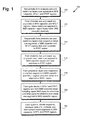
- Figure 1 shows a flow chart illustrating a method according to an embodiment of the present invention. Certain details and features have been left out of flowchart 100 that are apparent to a person of ordinary skill in the art. For example, a step may consist of one or more substeps or may involve specialized equipment or materials, as known in the art. Steps 170 through 182 indicated in flowchart 100 are sufficient to describe one embodiment of the present invention; however, other embodiments of the invention may utilize steps different from those shown in flowchart 100.
- processing steps shown in flowchart 100 are performed on a portion of processed wafer, which, prior to step 170, includes, among other things, a substrate, such as a silicon substrate, and isolation regions, such as shallow trench isolation (STI) regions, formed in MIM capacitor, N channel field effect transistor (NFET), and P channel FET (PFET) regions of the substrate.
- a substrate such as a silicon substrate
- isolation regions such as shallow trench isolation (STI) regions, formed in MIM capacitor, N channel field effect transistor (NFET), and P channel FET (PFET) regions of the substrate.
- STI shallow trench isolation
- MIM capacitor MIM capacitor
- NFET N channel field effect transistor
- PFET P channel FET
- structures 270 through 282 in Figures 2A through 2G illustrate the result of performing steps 170 through 182 of flowchart 100, respectively.
- structure 270 shows a semiconductor structure after processing step 170
- structure 272 shows structure 270 after the processing of step 172
- structure 274 shows structure 272 after the processing of step 174, and so forth.
- structure 270 of Figure 2A shows a structure including a substrate, after completion of step 170 of flowchart 100 in Figure 1 .
- substrate 202 which can be a silicon substrate, includes MIM capacitor region 204, NFET region 206, and PFET region 208.
- MIM capacitor region 204, NFET region 206, and PFET region 208 are regions of substrate 202 that are designated for MIM capacitor, NFET (e.g. NMOSFET), and PFET (e.g. PMOSFET) formation, respectively.
- isolation regions 210, 212, and 214 which can be, for example, STI regions, are formed in substrate 202. Isolation regions 210, 212, and 214 can comprise silicon oxide or other dielectric material.
- dielectric one layer 216 is formed over substrate 202 in MIM capacitor region 204, NFET region 206, and PFET region 208 and metal one layer 218 is formed over dielectric one layer 216.
- dielectric one layer 216 is situated over isolation regions 210, 212, and 214 and substrate 202.
- Dielectric one layer 216 can be, for example, a high dielectric constant (high-k) gate dielectric layer (e.g. a high-k dielectric layer that can be utilized for forming an NFET gate dielectric).
- high-k high dielectric constant
- Dielectric one layer 216 can comprise, for example, a metal oxide such as hafnium oxide (HfO 2 ), zirconium oxide (ZrO 2 ), or the like. Dielectric one layer 216 can be formed, for example, by depositing a high-k dielectric material, such as hafnium oxide or zirconium oxide, over substrate 202 by utilizing a physical vapor deposition (PVD) process, a chemical vapor deposition (CVD) process, or other deposition process.
- PVD physical vapor deposition
- CVD chemical vapor deposition
- metal one layer 218 can comprise a gate metal, such as a gate metal for an NFET gate.
- metal one layer 218 can comprise, for example, tantalum (Ta), tantalum nitride (TaN), titanium nitride (TiN), or other gate metal suitable for utilization in an NFET gate.
- metal one layer 218 is situated over dielectric one layer 216 in MIM capacitor region 204, NFET region 206, and PFET region 208.
- Metal one layer 218 can be formed, for example, by depositing a layer of tantalum, tantalum nitride, or titanium nitride over dielectric one layer 216 by utilizing a PVD process, a CVD process, or other deposition process.
- the result of step 170 of flowchart 100 is illustrated by structure 270 in Figure 2A .
- dielectric one segment 220 and metal one segment 222 are formed in MIM capacitor region 204 and dielectric one segment 224 and metal one segment 226 are formed in NFET region 206.
- dielectric one segment 220 is situated over isolation region 210 and metal one segment 222 is situated over dielectric segment 220 in MIM capacitor region 204.
- Metal one segment 222 can form a bottom electrode of a MIM capacitor that will be subsequently formed in MIM capacitor region 204.
- dielectric one segment 224 is situated over substrate 202 and isolation regions 210 and 212 and metal one segment 226 is situated over dielectric one segment 224 in NFET region 206.
- Dielectric one segments 220 and 224 and metal one segments 222 and 226 can be formed by, for example, appropriately patterning dielectric one layer 216 (shown in Figure 2A ) and metal one layer 218 (shown in Figure 2A ). During the patterning process, which can include a masking step and an etch step, metal one layer 218 and dielectric one layer 216 can be removed from PFET region 208.
- the result of step 172 of flowchart 100 is illustrated by structure 272 in Figure 2B .
- dielectric two layer 228 is formed over substrate 202 in PFET region 208, over metal one segment 226 in NFET region 206, over metal one segment 222 in MIM capacitor region 204, and over isolation regions 210, 212, and 214 in substrate 202.
- dielectric two layer 228 is situated over isolation regions 210, 212, and 214, substrate 202 in PFET region 208, metal one segment 226 in NFET region 206, and metal one segment 222 in MIM capacitor region 204.
- Dielectric two layer 228 can be, for example, a high-k gate dielectric layer (e.g.
- dielectric two layer 228 can comprise, for example, a metal oxide such as hafnium oxide, zirconium oxide, or the like. In one embodiment, dielectric two layer 228 can comprise the same dielectric material as dielectric one layer 216. In another embodiment, dielectric two layer 228 can comprise a different dielectric material than dielectric one layer 216. Dielectric two layer 228 can be formed, for example, by conformally depositing a high-k dielectric material, such as hafnium oxide or zirconium oxide, over substrate 202 by utilizing a PVD process, a CVD process, or other deposition process.
- a high-k dielectric material such as hafnium oxide or zirconium oxide
- metal two layer 230 can comprise a gate metal, such as a gate metal for a PFET gate.
- metal two layer 230 can comprise, for example, molybdenum (Mo), ruthenium (Ru), tantalum carbide nitride (TaCN), or other metal suitable for utilization in a PFET gate.
- Mo molybdenum
- Ru ruthenium
- TaCN tantalum carbide nitride
- metal two layer 230 is situated over dielectric two layer 228 in MIM capacitor region 204, NFET region 206, and PFET region 208.
- Metal two layer 230 can be formed, for example, by conformally depositing a layer of metal, such as molybdenum, ruthenium, or tantalum carbide nitride, over dielectric one layer 216 by utilizing a PVD process, a CVD process, or other deposition process.
- Metal two layer 230 can comprise a metal having a different workfunction compared to the metal in metal one layer 218 (shown in Figure 2A ).
- the result of step 174 of flowchart 100 is illustrated by structure 274 in Figure 2C .
- dielectric two segment 232 and metal two segment 234 are formed over metal one segment 222 in MIM capacitor region 204 and dielectric two segment 236 and metal two segment 238 are formed over substrate 202 in PFET region 208.
- dielectric two segment 232 is situated over metal one segment 222 and metal two segment 234 is situated over dielectric two segment 232 in MIM capacitor region 204.
- dielectric two segment 236 is situated over substrate 202 and isolation regions 212 and 214 and metal two segment 238 is situated over dielectric two segment 236 in PFET region 208.
- Dielectric two segments 232 and 236 and metal two segments 234 and 238 can be formed, for example, by appropriately patterning dielectric two layer 228 (shown in Figure 2C ) and metal two layer 230 (shown in Figure 2C ). During the patterning process, which can include a masking step and an etch step, metal two layer 230 and dielectric one layer 228 can be removed from NFET region 206 in the etch step. The result of step 176 of flowchart 100 is illustrated by structure 276 in Figure 2D .
- polysilicon layer 240 is formed over metal two segment 234 in MIM capacitor region 204, over metal one segment 226 NFET region 206, and over metal two segment 238 in PFET region 208.
- Polysilicon layer 240 is also formed over isolation region 210 in MIM capacitor region 204 and NFET region 206 and over isolation region 212 in NFET region 206 and PFET region 208.
- polysilicon layer 240 is situated over metal two segment 234, isolation region 210, metal one segment 226, isolation region 212, and metal two segment 238.
- Polysilicon layer 240 can comprise polysilicon and can be utilized for gate formation in NFET region 206 and PFET region 208 and for MIM capacitor formation in MIM capacitor region 204.
- Polysilicon layer 240 can be formed, for example, by conformally depositing a layer of polysilicon in MIM capacitor region 204, NFET region 206, and PFET region 208 by utilizing a low pressure chemical vapor deposition (LPCVD) process or other suitable deposition process.
- LPCVD low pressure chemical vapor deposition
- NFET gate stack 244 is formed in NFET region 206
- PFET gate stack 246 is formed in PFET region 208
- MIM capacitor stack 242 is formed in MIM capacitor region 204, where MIM capacitor stack 242 includes an upper MIM capacitor electrode and a MIM capacitor dielectric.
- MIM capacitor stack 242 includes dielectric two portion 247, which is a portion of dielectric two segment 232 (shown in Figure 2E ), metal two portion 248, which is a portion of metal two segment 234 (shown in Figure 2E ), and polysilicon segment 249.
- dielectric two portion 247 is situated over metal one segment 222
- metal two portion 248 is situated over dielectric two portion 247
- polysilicon segment 249 is situated over metal two portion 248.
- dielectric two portion 247 forms a MIM capacitor dielectric of MIM capacitor 245
- metal two portion 248 forms an upper electrode of MIM capacitor 245.
- metal one segment 222 which was formed at step 172 of flowchart 100, forms a lower electrode of MIM capacitor 245.
- NFET gate stack 244 includes dielectric one portion 250, which is situated over substrate 202, metal one portion 251, which is situated over dielectric one portion 250, and polysilicon segment 252, which is situated over metal one portion 215.
- dielectric one portion 250 forms an NFET gate dielectric
- metal one portion 251 forms an NFET.
- PFET gate stack 246 includes dielectric two portion 253, which is situated over substrate 202, metal two portion 254, which is situated over dielectric two portion 253, and polysilicon segment 255, which is situated over metal two portion 254.
- dielectric two portion 253 forms a PFET gate dielectric and metal two portion 254 forms an PFET metal gate.
- MIM capacitor stack 242 can be formed by appropriately patterning metal two segment 234 and dielectric two segment 232 (shown in Figure 2D ), NFET gate stack 244 can be formed by appropriately patterning metal one segment 226 and dielectric one segment 224 (shown in Figure 2D ), and PFET gate stack 246 can be formed by appropriately patterning metal two segment 238 and dielectric two segment 236 (shown in Figure 2D ).
- the patterning process utilized to form MIM capacitor stack 242, NFET gate stack 244, and PFET gate stack 246 can include a masking step and an etching step.
- the result of step 180 of flowchart 100 is illustrated by structure 280 in Figure 2F .
- step 182 of flowchart 100 spacers 256 and 257, silicide segment 261, contacts 267 and 268, and interconnect metal segments 269 and 283 are formed in MIM capacitor region 204; spacers 258, silicide segments 262 and 264, and contacts and interconnect metal segments are formed in NFET region 206; spacers 260, silicide segments 263 and 265, and contacts and interconnect metal segments are formed in PFET region 208; and interlayer dielectric 266 is formed in MIM capacitor region 204, NFET region 206 and PFET region 208.
- source/drain regions are formed in substrate 202 adjacent to NFET gate stack 244 in NFET region 206 and adjacent to PFET gate stack 246 in PFET region 208.
- spacers 256 are situated adjacent to respective sides of MIM capacitor stack 242
- spacer 257 is situated adjacent to metal one segment 222 and dielectric one segment 220
- spacers 258 are situated adjacent to respective sides of NFET gate stack 244
- spacers 260 are situated adjacent to respective sides of PFET gate stack 246.
- Spacers 256, 257, 258, and 260 can comprise silicon oxide or other dielectric material as known in the art.
- Spacers 256, 257, 258, and 260 can be formed, for example, by conformally depositing a layer of dielectric material, such as silicon oxide, over MIM capacitor stack 242, metal one segment 222, NFET gate stack 244, and PFET gate stack 246, by utilizing a CVD process or other deposition process and appropriately etching the layer of dielectric material in an etch-back process.
- a layer of dielectric material such as silicon oxide
- silicide segment 261 is situated on polysilicon segment 249 of MIM capacitor stack 242, silicide segment 262 is situated on polysilicon segment 252 in NFET gate stack 244, silicide segments 264 are situated on substrate 202 adjacent to NFET gate stack 244, silicide segment 263 is situated on polysilicon segment 255 in PFET gate stack 246, and silicide segments 265 are situated on substrate 202 adjacent to PFET gate stack 246. It is noted that the silicide segments can extend into the feature on which they are formed. Thus, for example, silicide segment 261 can extend into polysilicon segment 249 of MIM capacitor stack 242.
- Silicide segments 261, 262, 263, 264, and 265 can comprise a metal silicide, such as, for example, nickel silicide or cobalt silicide, and can be formed in a manner known in the art. Further shown in Figure 2G , interlayer dielectric 266 is situated over MIM capacitor 245, NFET gate stack 244, PFET gate stack 246, isolation regions 210, 212, and 214, and substrate 202.
- metal silicide such as, for example, nickel silicide or cobalt silicide
- Interlayer dielectric 266 can comprise silicon oxide or other dielectric material and can be formed, for example, by utilizing a CVD process or other deposition process to deposit a layer of dielectric material, such as silicon oxide, over MIM capacitor 245, NFET gate stack 244, PFET gate stack 246, isolation regions 210, 212, and 214, and substrate 202.
- contact 267 is situated on metal one segment 222 of MIM capacitor 245 and contact 268 is situated on silicide segment 261 of MIM capacitor 245.
- Contacts such as contacts 267 and 268 can be formed in interlayer dielectric 266 by etching a contact via in interlayer dielectric 266 and filling the contact via with tungsten or other metal or metal stack as is known in the art.
- interconnect metal segment 269 is situated on contact 267
- interconnect metal segment 283 is situated on contact 268, and interconnect metal segments 269 and 283 are also situated over interlayer dielectric 266.
- Interconnect metal segments 269 and 283 are situated in interconnect metal layer 284, which can be a first interconnect metal layer in the semiconductor die.
- Interconnect metal segments 269 and 283 can comprise, for example, a metal such as aluminum or copper and can be formed by depositing and patterning a layer of metal over interlayer dielectric 266 in a manner known in the art.
- interconnect metal segment 269 is electrically connected by contact 267 to metal one segment 222, which forms the lower electrode of MIM capacitor 245.
- interconnect metal segment 269 provides electrical connectivity to the lower electrode of MIM capacitor 245.
- interconnect metal segment 283 is electrically connected by contact 268 to silicide segment 261, which is electrically connected by polysilicon segment 249 to metal two portion 248, which forms the upper electrode of MIM capacitor 245.
- interconnect metal segment 283 provides electrical connectivity to the upper electrode of MIM capacitor 245.
- NFET 241 and PFET 243 are formed, where NFET 241 (e.g.
- an NMOSFET includes NFET gate stack 244 and source/drain regions (not shown in Figure 2G ) and PFET 243 (e.g. a PMOSFET) includes PFET gate stack 246 and source/drain regions (not shown in Figure 2G ).
- MIM capacitor 245 is situated between interconnect metal layer 284 (i.e. a first interconnect metal layer in the semiconductor die) and substrate 202.
- interconnect metal layer 284 i.e. a first interconnect metal layer in the semiconductor die
- the lower and upper electrodes of MIM capacitor 245 do not overlie an interconnect metal layer in the semiconductor die.
- contacts 267 and 268 and interconnect metal segments 269 and 283 are specifically discussed herein to preserve brevity.
- the result of step 182 of flowchart 100 is illustrated by structure 282 in Figure 2G .
- MIM capacitor stack 242 corresponds to PFET gate stack 246.
- metal two portion 248 of MIM capacitor stack 242 i.e. the upper electrode of MIM capacitor 245 can comprise the same gate metal as the metal gate in PFET gate stack 246.
- metal one segment 222 i.e. the lower electrode of MIM capacitor 245) can comprise the same gate metal as the metal gate in NFET gate stack 244.
- the upper electrode of MIM capacitor 245 can comprise the same gate metal as the metal gate in NFET gate stack 244 and the lower electrode of MIM capacitor 245 can comprise the same gate metal as the metal gate in PFET gate stack 246.
- an embodiment of the invention's MIM capacitor 245 is compatible with a high-k metal gate process for advanced process technologies, such as 45.0 nanometer (nm) and smaller process technologies. Also, by utilizing a high-k gate dielectric material for a MIM capacitor dielectric and gate metal for lower and upper MIM capacitor electrodes, an embodiment of the invention's MIM capacitor 245 can provide a capacitance density greater than approximately 20.0 femtofarads (fF)/um 2 , thereby advantageously reducing MIM capacitor die area.
- fF femtofarads
- an embodiment of the present invention can advantageously form a MIM capacitor (e.g. MIM capacitor 245) without requiring any additional masks other than the masks required to form the NFET and PFET gate stacks. Also, by forming a MIM capacitor concurrently with NFET and PFET gate stacks, the capacitance of an embodiment of the invention's MIM capacitor is easier to control compared to the capacitance of a conventional MIM capacitor that is formed between interconnect metal layers in a semiconductor die during BEOL processing.
- the present invention provides a MIM capacitor that utilizes gate metal for upper and lower electrodes and a gate dielectric material, such as a high-k gate dielectric material, for a MIM capacitor dielectric.
- the invention's MIM capacitor can be advantageously formed concurrently with NFET and PFET gate stacks without requiring an additional mask other than the masks required to form the NFET and PFET gate stacks.
- the present invention provides a MIM capacitor that can be fabricated at a significantly lower cost compared to a conventional MIM capacitor that is fabricated interconnect metal layers in a semiconductor die during BEOL processing.
- the present invention provides a MIM capacitor having a capacitance that is easier to control compared to the capacitance of a conventional MIM capacitor.
Landscapes
- Semiconductor Integrated Circuits (AREA)
- Metal-Oxide And Bipolar Metal-Oxide Semiconductor Integrated Circuits (AREA)
Abstract
Description
- The present invention is generally in the field of semiconductors. More particularly, the invention is in the field of fabrication of capacitors in semiconductor dies.
- Metal-insulator-metal (MIM) capacitors have been extensively utilized in the fabrication of integrated analog and mixed signal circuits on semiconductor dies. A MIM capacitor typically includes a MIM capacitor dielectric situated between lower and upper metal plates, which form the electrodes of the MIM capacitor. Conventionally, MIM capacitors can be fabricated on semiconductor dies during back-end-of-line (BEOL) processing.
- A conventional MIM capacitor can be fabricated, for example, by inserting a specialized dielectric layer for a MIM capacitor dielectric and specialized metal layers for lower and upper MIM capacitor electrodes in the otherwise unused "vertical" space available between interconnect metal layers on a semiconductor die during BEOL processing. However, inserting the specialized dielectric and metal layers required to form the MIM capacitor dielectric and the bottom and upper MIM capacitor electrodes during BEOL processing can require multiple process steps and masks, which can undesirably increase manufacturing cost.
- A method for fabricating a MIM capacitor using gate metal for electrode and related structure are provided. Features, advantages and various embodiments of the present invention are shown in and/or described in connection with at least one of the drawings, as set forth more completely in the claims.
- According to an aspect, a method for fabricating a MIM capacitor in a semiconductor die comprises:
- forming a dielectric one segment over a substrate and a metal one segment over said dielectric one segment, said metal one segment forming a lower electrode of said MIM capacitor;
- forming a dielectric two segment over said metal one segment and a metal two segment over said dielectric two segment, a portion of said metal two segment forming an upper electrode of said MIM capacitor;
- said metal one segment comprising a first gate metal.
- Advantageously, said metal two segment comprises a second gate metal.
- Advantageously, said first gate metal is different than said second gate metal.
- Advantageously, said dielectric one segment is formed over an isolation region in said substrate.
- Advantageously, the method further comprises:
- forming a polysilicon layer over said metal two segment; and
- patterning said polysilicon layer, said metal two segment, and said dielectric two segment to form a MIM capacitor stack, wherein said MIM capacitor stack includes a polysilicon segment overlying said portion of said metal two segment.
- Advantageously, the method further comprises forming a silicide segment on said polysilicon segment.
- Advantageously, the method further comprises forming spacers adjacent to respective sides of said MIM capacitor stack.
- Advantageously, said metal two segment does not overlie an interconnect metal layer in said semiconductor die.
- Advantageously, said dielectric two segment comprises a high-k dielectric.
- Advantageously, said dielectric one segment comprises a high-k dielectric.
- According to an aspect, a MIM capacitor in a semiconductor die is provided, said MIM capacitor comprising:
- a lower electrode of said MIM capacitor situated over a substrate, said lower electrode of said MIM capacitor comprising a first gate metal;
- a MIM capacitor dielectric situated over said lower electrode of said MIM capacitor;
- an upper electrode of said MIM capacitor situated over said MIM capacitor dielectric.
- Advantageously, said upper electrode of said MIM capacitor comprises a second gate metal.
- Advantageously, said first gate metal is different than said second gate metal.
- Advantageously, said lower electrode of said MIM capacitor is situated over an isolation region in said substrate.
- Advantageously, the capacitor further comprises a polysilicon segment situated over said upper electrode of said MIM capacitor.
- Advantageously, the capacitor further comprises a high-k dielectric situated between said lower electrode of said MIM capacitor and said substrate.
- Advantageously, said MIM capacitor dielectric is a high-k dielectric.
- Advantageously, the capacitor further comprises spacers situated adjacent to respective sides of said upper electrode of said MIM capacitor.
- Advantageously, the capacitor further comprisesa silicide segment situated on said polysilicon segment.
- Advantageously, said upper electrode of said MIM capacitor does not overlie an interconnect metal layer in said semiconductor die.
-
-
Figure 1 shows a flowchart illustrating the steps taken to implement an embodiment of the present invention. -
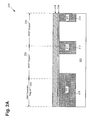
Figure 2A illustrates a cross-sectional view, which includes a portion of a wafer processed according to an embodiment of the invention, corresponding to an initial step in the flowchart inFigure 1 . -
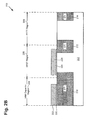
Figure 2B illustrates a cross-sectional view, which includes a portion of a wafer processed according to an embodiment of the invention, corresponding to an intermediate step in the flowchart inFigure 1 . -
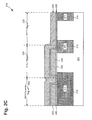
Figure 2C illustrates a cross-sectional view, which includes a portion of a wafer processed according to an embodiment of the invention, corresponding to an intermediate step in the flowchart inFigure 1 . -
Figure 2D illustrates a cross-sectional view, which includes a portion of a wafer processed according to an embodiment of the invention, corresponding to an intermediate step in the flowchart inFigure 1 . -
Figure 2E illustrates a cross-sectional view, which includes a portion of a wafer processed according to an embodiment of the invention, corresponding to an intermediate step in the flowchart inFigure 1 . -
Figure 2F illustrates a cross-sectional view, which includes a portion of a wafer processed according to an embodiment of the invention, corresponding to an intermediate step in the flowchart inFigure 1 . -
Figure 2G illustrates a cross-sectional view, which includes a portion of a wafer processed according to an embodiment of the invention, corresponding to a final step in the flowchart inFigure 1 . - The present invention is directed to a method for fabricating a MIM capacitor using gate metal for electrode and related structure. The following description contains specific information pertaining to the implementation of the present invention. One skilled in the art will recognize that the present invention may be implemented in a manner different from that specifically discussed in the present application. Moreover, some of the specific details of the invention are not discussed in order not to obscure the invention.
- The drawings in the present application and their accompanying detailed description are directed to merely exemplary embodiments of the invention. To maintain brevity, other embodiments of the present invention are not specifically described in the present application and are not specifically illustrated by the present drawings.
-
Figure 1 shows a flow chart illustrating a method according to an embodiment of the present invention. Certain details and features have been left out offlowchart 100 that are apparent to a person of ordinary skill in the art. For example, a step may consist of one or more substeps or may involve specialized equipment or materials, as known in the art.Steps 170 through 182 indicated inflowchart 100 are sufficient to describe one embodiment of the present invention; however, other embodiments of the invention may utilize steps different from those shown inflowchart 100. It is noted that the processing steps shown inflowchart 100 are performed on a portion of processed wafer, which, prior tostep 170, includes, among other things, a substrate, such as a silicon substrate, and isolation regions, such as shallow trench isolation (STI) regions, formed in MIM capacitor, N channel field effect transistor (NFET), and P channel FET (PFET) regions of the substrate. The wafer is also referred to simply as a wafer or a semiconductor die or simply a die in the present application. - Moreover,
structures 270 through 282 inFigures 2A through 2G illustrate the result of performingsteps 170 through 182 offlowchart 100, respectively. For example,structure 270 shows a semiconductor structure after processingstep 170,structure 272 showsstructure 270 after the processing ofstep 172,structure 274 showsstructure 272 after the processing ofstep 174, and so forth. - Referring now to
Figure 2A ,structure 270 ofFigure 2A shows a structure including a substrate, after completion ofstep 170 offlowchart 100 inFigure 1 . Instructure 270,substrate 202, which can be a silicon substrate, includesMIM capacitor region 204,NFET region 206, andPFET region 208.MIM capacitor region 204,NFET region 206, andPFET region 208 are regions ofsubstrate 202 that are designated for MIM capacitor, NFET (e.g. NMOSFET), and PFET (e.g. PMOSFET) formation, respectively. Instructure 270,isolation regions substrate 202.Isolation regions - Continuing to refer to step 170 in
Figure 1 andstructure 270 inFigure 2A , atstep 170 offlowchart 100, dielectric onelayer 216 is formed oversubstrate 202 inMIM capacitor region 204,NFET region 206, andPFET region 208 and metal onelayer 218 is formed over dielectric onelayer 216. As shown inFigure 2A , dielectric onelayer 216 is situated overisolation regions substrate 202. Dielectric onelayer 216 can be, for example, a high dielectric constant (high-k) gate dielectric layer (e.g. a high-k dielectric layer that can be utilized for forming an NFET gate dielectric). Dielectric onelayer 216 can comprise, for example, a metal oxide such as hafnium oxide (HfO2), zirconium oxide (ZrO2), or the like. Dielectric onelayer 216 can be formed, for example, by depositing a high-k dielectric material, such as hafnium oxide or zirconium oxide, oversubstrate 202 by utilizing a physical vapor deposition (PVD) process, a chemical vapor deposition (CVD) process, or other deposition process. - Also shown in
Figure 2A , metal onelayer 218 can comprise a gate metal, such as a gate metal for an NFET gate. In an embodiment of the invention, metal onelayer 218 can comprise, for example, tantalum (Ta), tantalum nitride (TaN), titanium nitride (TiN), or other gate metal suitable for utilization in an NFET gate. As shown, metal onelayer 218 is situated over dielectric onelayer 216 inMIM capacitor region 204,NFET region 206, andPFET region 208. Metal onelayer 218 can be formed, for example, by depositing a layer of tantalum, tantalum nitride, or titanium nitride over dielectric onelayer 216 by utilizing a PVD process, a CVD process, or other deposition process. The result ofstep 170 offlowchart 100 is illustrated bystructure 270 inFigure 2A . - Referring to step 172 in
Figure 1 andstructure 272 inFigure 2B , atstep 172 offlowchart 100, dielectric onesegment 220 and metal onesegment 222 are formed inMIM capacitor region 204 and dielectric onesegment 224 and metal onesegment 226 are formed inNFET region 206. As shown inFigure 2B , dielectric onesegment 220 is situated overisolation region 210 and metal onesegment 222 is situated overdielectric segment 220 inMIM capacitor region 204. Metal onesegment 222 can form a bottom electrode of a MIM capacitor that will be subsequently formed inMIM capacitor region 204. Also shown inFigure 2B , dielectric onesegment 224 is situated oversubstrate 202 andisolation regions segment 226 is situated over dielectric onesegment 224 inNFET region 206.Dielectric one segments segments Figure 2A ) and metal one layer 218 (shown inFigure 2A ). During the patterning process, which can include a masking step and an etch step, metal onelayer 218 and dielectric onelayer 216 can be removed fromPFET region 208. The result ofstep 172 offlowchart 100 is illustrated bystructure 272 inFigure 2B . - Referring to step 174 in
Figure 1 andstructure 274 inFigure 2C , atstep 174 offlowchart 100, dielectric twolayer 228 is formed oversubstrate 202 inPFET region 208, over metal onesegment 226 inNFET region 206, over metal onesegment 222 inMIM capacitor region 204, and overisolation regions substrate 202. As shown inFigure 2C , dielectric twolayer 228 is situated overisolation regions substrate 202 inPFET region 208, metal onesegment 226 inNFET region 206, and metal onesegment 222 inMIM capacitor region 204. Dielectric twolayer 228 can be, for example, a high-k gate dielectric layer (e.g. a high-k dielectric layer that can be utilized for forming an PFET gate dielectric). In an embodiment of the invention, dielectric twolayer 228 can comprise, for example, a metal oxide such as hafnium oxide, zirconium oxide, or the like. In one embodiment, dielectric twolayer 228 can comprise the same dielectric material as dielectric onelayer 216. In another embodiment, dielectric twolayer 228 can comprise a different dielectric material than dielectric onelayer 216. Dielectric twolayer 228 can be formed, for example, by conformally depositing a high-k dielectric material, such as hafnium oxide or zirconium oxide, oversubstrate 202 by utilizing a PVD process, a CVD process, or other deposition process. - Also shown in
Figure 2C , metal twolayer 230 can comprise a gate metal, such as a gate metal for a PFET gate. In an embodiment of the invention, metal twolayer 230 can comprise, for example, molybdenum (Mo), ruthenium (Ru), tantalum carbide nitride (TaCN), or other metal suitable for utilization in a PFET gate. As shown, metal twolayer 230 is situated over dielectric twolayer 228 inMIM capacitor region 204,NFET region 206, andPFET region 208. Metal twolayer 230 can be formed, for example, by conformally depositing a layer of metal, such as molybdenum, ruthenium, or tantalum carbide nitride, over dielectric onelayer 216 by utilizing a PVD process, a CVD process, or other deposition process. Metal twolayer 230 can comprise a metal having a different workfunction compared to the metal in metal one layer 218 (shown inFigure 2A ). The result ofstep 174 offlowchart 100 is illustrated bystructure 274 inFigure 2C . - Referring to step 176 in
Figure 1 andstructure 276 inFigure 2D , atstep 176 offlowchart 100, dielectric twosegment 232 and metal twosegment 234 are formed over metal onesegment 222 inMIM capacitor region 204 and dielectric twosegment 236 and metal twosegment 238 are formed oversubstrate 202 inPFET region 208. As shown inFigure 2D , dielectric twosegment 232 is situated over metal onesegment 222 and metal twosegment 234 is situated over dielectric twosegment 232 inMIM capacitor region 204. Also shown inFigure 2D , dielectric twosegment 236 is situated oversubstrate 202 andisolation regions segment 238 is situated over dielectric twosegment 236 inPFET region 208. Dielectric twosegments segments Figure 2C ) and metal two layer 230 (shown inFigure 2C ). During the patterning process, which can include a masking step and an etch step, metal twolayer 230 and dielectric onelayer 228 can be removed fromNFET region 206 in the etch step. The result ofstep 176 offlowchart 100 is illustrated bystructure 276 inFigure 2D . - Referring to step 178 in
Figure 1 andstructure 278 inFigure 2E , atstep 178 offlowchart 100,polysilicon layer 240 is formed over metal twosegment 234 inMIM capacitor region 204, over metal onesegment 226NFET region 206, and over metal twosegment 238 inPFET region 208.Polysilicon layer 240 is also formed overisolation region 210 inMIM capacitor region 204 andNFET region 206 and overisolation region 212 inNFET region 206 andPFET region 208. As shown inFigure 2E ,polysilicon layer 240 is situated over metal twosegment 234,isolation region 210, metal onesegment 226,isolation region 212, and metal twosegment 238.Polysilicon layer 240 can comprise polysilicon and can be utilized for gate formation inNFET region 206 andPFET region 208 and for MIM capacitor formation inMIM capacitor region 204.Polysilicon layer 240 can be formed, for example, by conformally depositing a layer of polysilicon inMIM capacitor region 204,NFET region 206, andPFET region 208 by utilizing a low pressure chemical vapor deposition (LPCVD) process or other suitable deposition process. The result ofstep 178 offlowchart 100 is illustrated bystructure 278 inFigure 2E . - Referring to step 180 in
Figure 1 andstructure 280 inFigure 2F , atstep 180 offlowchart 100,NFET gate stack 244 is formed inNFET region 206,PFET gate stack 246 is formed inPFET region 208, andMIM capacitor stack 242 is formed inMIM capacitor region 204, whereMIM capacitor stack 242 includes an upper MIM capacitor electrode and a MIM capacitor dielectric.MIM capacitor stack 242 includes dielectric twoportion 247, which is a portion of dielectric two segment 232 (shown inFigure 2E ), metal twoportion 248, which is a portion of metal two segment 234 (shown inFigure 2E ), andpolysilicon segment 249. As shown inFigure 2F , inMIM capacitor region 204, dielectric twoportion 247 is situated over metal onesegment 222, metal twoportion 248 is situated over dielectric twoportion 247, andpolysilicon segment 249 is situated over metal twoportion 248. As shown inFigure 2F , dielectric twoportion 247 forms a MIM capacitor dielectric ofMIM capacitor 245 and metal twoportion 248 forms an upper electrode ofMIM capacitor 245. Also, metal onesegment 222, which was formed atstep 172 offlowchart 100, forms a lower electrode ofMIM capacitor 245. - Also shown in
Figure 2F ,NFET gate stack 244 includes dielectric oneportion 250, which is situated oversubstrate 202, metal oneportion 251, which is situated over dielectric oneportion 250, andpolysilicon segment 252, which is situated over metal one portion 215. InNFET gate stack 244, dielectric oneportion 250 forms an NFET gate dielectric and metal oneportion 251 forms an NFET. Further shown inFigure 2F ,PFET gate stack 246 includes dielectric twoportion 253, which is situated oversubstrate 202, metal twoportion 254, which is situated over dielectric twoportion 253, andpolysilicon segment 255, which is situated over metal twoportion 254. InPFET gate stack 246, dielectric twoportion 253 forms a PFET gate dielectric and metal twoportion 254 forms an PFET metal gate. -
MIM capacitor stack 242 can be formed by appropriately patterning metal twosegment 234 and dielectric two segment 232 (shown inFigure 2D ),NFET gate stack 244 can be formed by appropriately patterning metal onesegment 226 and dielectric one segment 224 (shown inFigure 2D ), andPFET gate stack 246 can be formed by appropriately patterning metal twosegment 238 and dielectric two segment 236 (shown inFigure 2D ). The patterning process utilized to formMIM capacitor stack 242,NFET gate stack 244, andPFET gate stack 246 can include a masking step and an etching step. The result ofstep 180 offlowchart 100 is illustrated bystructure 280 inFigure 2F . - Referring to step 182 in
Figure 1 andstructure 282 inFigure 2G , atstep 182 offlowchart 100,spacers contacts interconnect metal segments MIM capacitor region 204;spacers 258,silicide segments NFET region 206;spacers 260,silicide segments PFET region 208; andinterlayer dielectric 266 is formed inMIM capacitor region 204,NFET region 206 andPFET region 208. Also atstep 182 offlowchart 100, source/drain regions (not shown inFigure 2G ) are formed insubstrate 202 adjacent toNFET gate stack 244 inNFET region 206 and adjacent to PFETgate stack 246 inPFET region 208. - As shown in
Figure 2G ,spacers 256 are situated adjacent to respective sides ofMIM capacitor stack 242,spacer 257 is situated adjacent to metal onesegment 222 and dielectric onesegment 220,spacers 258 are situated adjacent to respective sides ofNFET gate stack 244, andspacers 260 are situated adjacent to respective sides ofPFET gate stack 246.Spacers Spacers MIM capacitor stack 242, metal onesegment 222,NFET gate stack 244, andPFET gate stack 246, by utilizing a CVD process or other deposition process and appropriately etching the layer of dielectric material in an etch-back process. - Also shown in
Figure 2G , silicide segment 261 is situated onpolysilicon segment 249 ofMIM capacitor stack 242,silicide segment 262 is situated onpolysilicon segment 252 inNFET gate stack 244,silicide segments 264 are situated onsubstrate 202 adjacent toNFET gate stack 244,silicide segment 263 is situated onpolysilicon segment 255 inPFET gate stack 246, andsilicide segments 265 are situated onsubstrate 202 adjacent to PFETgate stack 246. It is noted that the silicide segments can extend into the feature on which they are formed. Thus, for example, silicide segment 261 can extend intopolysilicon segment 249 ofMIM capacitor stack 242.Silicide segments Figure 2G ,interlayer dielectric 266 is situated overMIM capacitor 245,NFET gate stack 244,PFET gate stack 246,isolation regions substrate 202.Interlayer dielectric 266 can comprise silicon oxide or other dielectric material and can be formed, for example, by utilizing a CVD process or other deposition process to deposit a layer of dielectric material, such as silicon oxide, overMIM capacitor 245,NFET gate stack 244,PFET gate stack 246,isolation regions substrate 202. - Also shown in
Figure 2G , contact 267 is situated on metal onesegment 222 ofMIM capacitor 245 and contact 268 is situated on silicide segment 261 ofMIM capacitor 245. Contacts, such ascontacts interlayer dielectric 266 by etching a contact via ininterlayer dielectric 266 and filling the contact via with tungsten or other metal or metal stack as is known in the art. Further shown inFigure 2G ,interconnect metal segment 269 is situated oncontact 267,interconnect metal segment 283 is situated oncontact 268, andinterconnect metal segments interlayer dielectric 266.Interconnect metal segments interconnect metal layer 284, which can be a first interconnect metal layer in the semiconductor die.Interconnect metal segments interlayer dielectric 266 in a manner known in the art. - As shown in
Figure 2G ,interconnect metal segment 269 is electrically connected bycontact 267 to metal onesegment 222, which forms the lower electrode ofMIM capacitor 245. Thus,interconnect metal segment 269 provides electrical connectivity to the lower electrode ofMIM capacitor 245. Also shown inFigure 2G ,interconnect metal segment 283 is electrically connected bycontact 268 to silicide segment 261, which is electrically connected bypolysilicon segment 249 to metal twoportion 248, which forms the upper electrode ofMIM capacitor 245. Thus,interconnect metal segment 283 provides electrical connectivity to the upper electrode ofMIM capacitor 245. Thus, as further shown inFigure 2G ,NFET 241 andPFET 243 are formed, where NFET 241 (e.g. an NMOSFET) includesNFET gate stack 244 and source/drain regions (not shown inFigure 2G ) and PFET 243 (e.g. a PMOSFET) includesPFET gate stack 246 and source/drain regions (not shown inFigure 2G ). - Also, as shown in
Figure 2G ,MIM capacitor 245 is situated between interconnect metal layer 284 (i.e. a first interconnect metal layer in the semiconductor die) andsubstrate 202. Thus, the lower and upper electrodes ofMIM capacitor 245 do not overlie an interconnect metal layer in the semiconductor die. It is noted that inFigure 2G , onlycontacts interconnect metal segments step 182 offlowchart 100 is illustrated bystructure 282 inFigure 2G . - In an embodiment of the invention shown in
Figures 2A through 2G ,MIM capacitor stack 242 corresponds to PFETgate stack 246. Thus, metal twoportion 248 of MIM capacitor stack 242 (i.e. the upper electrode of MIM capacitor 245) can comprise the same gate metal as the metal gate inPFET gate stack 246. Also, in the embodiment of the invention shown inFigures 2A through 2G , metal one segment 222 (i.e. the lower electrode of MIM capacitor 245) can comprise the same gate metal as the metal gate inNFET gate stack 244. However, in another embodiment, the process for formingMIM capacitor 245,NFET gate stack 244, andPFET gate stack 246 and be performed in a different order, whereinMIM capacitor stack 242 can correspond toNFET gate stack 244. Thus, in such embodiment, the upper electrode ofMIM capacitor 245 can comprise the same gate metal as the metal gate inNFET gate stack 244 and the lower electrode ofMIM capacitor 245 can comprise the same gate metal as the metal gate inPFET gate stack 246. - By utilizing a high-k gate dielectric material for a MIM capacitor dielectric and gate metal for lower and upper MIM capacitor electrodes, the process for forming an embodiment of the invention's
MIM capacitor 245 is compatible with a high-k metal gate process for advanced process technologies, such as 45.0 nanometer (nm) and smaller process technologies. Also, by utilizing a high-k gate dielectric material for a MIM capacitor dielectric and gate metal for lower and upper MIM capacitor electrodes, an embodiment of the invention'sMIM capacitor 245 can provide a capacitance density greater than approximately 20.0 femtofarads (fF)/um2, thereby advantageously reducing MIM capacitor die area. - By forming a MIM capacitor in a MIM capacitor region of a substrate while concurrently forming an NFET gate stack in an NFET region of the substrate and a PFET gate stack in a PFET region of the substrate, an embodiment of the present invention can advantageously form a MIM capacitor (e.g. MIM capacitor 245) without requiring any additional masks other than the masks required to form the NFET and PFET gate stacks. Also, by forming a MIM capacitor concurrently with NFET and PFET gate stacks, the capacitance of an embodiment of the invention's MIM capacitor is easier to control compared to the capacitance of a conventional MIM capacitor that is formed between interconnect metal layers in a semiconductor die during BEOL processing.
- Thus, as discussed above, the present invention provides a MIM capacitor that utilizes gate metal for upper and lower electrodes and a gate dielectric material, such as a high-k gate dielectric material, for a MIM capacitor dielectric. As such, the invention's MIM capacitor can be advantageously formed concurrently with NFET and PFET gate stacks without requiring an additional mask other than the masks required to form the NFET and PFET gate stacks. By not requiring an additional mask, the present invention provides a MIM capacitor that can be fabricated at a significantly lower cost compared to a conventional MIM capacitor that is fabricated interconnect metal layers in a semiconductor die during BEOL processing. Also, the present invention provides a MIM capacitor having a capacitance that is easier to control compared to the capacitance of a conventional MIM capacitor.
- From the above description of the invention it is manifest that various techniques can be used for implementing the concepts of the present invention without departing from its scope. Moreover, while the invention has been described with specific reference to certain embodiments, a person of ordinary skill in the art would appreciate that changes can be made in form and detail without departing from the spirit and the scope of the invention. Thus, the described embodiments are to be considered in all respects as illustrative and not restrictive. It should also be understood that the invention is not limited to the particular embodiments described herein but is capable of many rearrangements, modifications, and substitutions without departing from the scope of the invention.
Claims (15)
- A method for fabricating a MIM capacitor in a semiconductor die, said method comprising:forming a dielectric one segment over a substrate and a metal one segment over said dielectric one segment, said metal one segment forming a lower electrode of said MIM capacitor;forming a dielectric two segment over said metal one segment and a metal two segment over said dielectric two segment, a portion of said metal two segment forming an upper electrode of said MIM capacitor;said metal one segment comprising a first gate metal.
- The method of claim 1, wherein said metal two segment comprises a second gate metal.
- The method of claim 2, wherein said first gate metal is different than said second gate metal.
- The method of claim 1, wherein said dielectric one segment is formed over an isolation region in said substrate.
- The method of claim 1 further comprising:forming a polysilicon layer over said metal two segment; andpatterning said polysilicon layer, said metal two segment, and said dielectric two segment to form a MIM capacitor stack, wherein said MIM capacitor stack includes a polysilicon segment overlying said portion of said metal two segment.
- The method of claim 5 further comprising forming a silicide segment on said polysilicon segment.
- The method of claim 5 further comprising forming spacers adjacent to respective sides of said MIM capacitor stack.
- The method of claim 1, wherein said metal two segment does not overlie an interconnect metal layer in said semiconductor die.
- The method of claim 1, wherein said dielectric two segment comprises a high-k dielectric.
- The method of claim 1, wherein said dielectric one segment comprises a high-k dielectric.
- A MIM capacitor in a semiconductor die, said MIM capacitor comprising:a lower electrode of said MIM capacitor situated over a substrate, said lower electrode of said MIM capacitor comprising a first gate metal;a MIM capacitor dielectric situated over said lower electrode of said MIM capacitor;an upper electrode of said MIM capacitor situated over said MIM capacitor dielectric.
- The MIM capacitor of claim 11, wherein said upper electrode of said MIM capacitor comprises a second gate metal.
- The MIM capacitor of claim 12, wherein said first gate metal is different than said second gate metal.
- The MIM capacitor of claim 11, wherein said lower electrode of said MIM capacitor is situated over an isolation region in said substrate.
- The MIM capacitor of claim 11 further comprising a polysilicon segment situated over said upper electrode of said MIM capacitor.
Applications Claiming Priority (1)
| Application Number | Priority Date | Filing Date | Title |
|---|---|---|---|
| US12/462,692 US8614497B2 (en) | 2009-08-07 | 2009-08-07 | Method for fabricating a MIM capacitor using gate metal for electrode and related structure |
Publications (2)
| Publication Number | Publication Date |
|---|---|
| EP2282341A2 true EP2282341A2 (en) | 2011-02-09 |
| EP2282341A3 EP2282341A3 (en) | 2013-08-28 |
Family
ID=43303902
Family Applications (1)
| Application Number | Title | Priority Date | Filing Date |
|---|---|---|---|
| EP10008149.6A Withdrawn EP2282341A3 (en) | 2009-08-07 | 2010-08-04 | Method for fabricating a MIM capacitor using gate metal for electrode and related structure |
Country Status (4)
| Country | Link |
|---|---|
| US (1) | US8614497B2 (en) |
| EP (1) | EP2282341A3 (en) |
| CN (1) | CN101996864B (en) |
| TW (1) | TWI438843B (en) |
Families Citing this family (19)
| Publication number | Priority date | Publication date | Assignee | Title |
|---|---|---|---|---|
| US8558300B2 (en) * | 2009-11-06 | 2013-10-15 | Broadcom Corporation | Method for fabricating a flash memory cell utilizing a high-K metal gate process and related structure |
| IT1397231B1 (en) * | 2009-12-30 | 2013-01-04 | St Microelectronics Srl | MIM CONDENSER WITH PLATE WITH HIGH MELT POINT |
| US8963223B2 (en) * | 2010-03-01 | 2015-02-24 | Broadcom Corporation | Scalable integrated MIM capacitor using gate metal |
| US8482078B2 (en) * | 2011-05-10 | 2013-07-09 | International Business Machines Corporation | Integrated circuit diode |
| CN102956437B (en) * | 2011-08-17 | 2015-05-13 | 中芯国际集成电路制造(上海)有限公司 | Capacitor and method for manufacturing capacitor on semiconductor device with metal grid electrode |
| US9041153B2 (en) * | 2011-09-29 | 2015-05-26 | Broadcom Corporation | MIM capacitor having a local interconnect metal electrode and related structure |
| CN103545181B (en) * | 2012-07-11 | 2017-06-16 | 中芯国际集成电路制造(上海)有限公司 | A kind of method that use dummy gate electrode manufactures semiconductor devices |
| US9012966B2 (en) * | 2012-11-21 | 2015-04-21 | Qualcomm Incorporated | Capacitor using middle of line (MOL) conductive layers |
| US9969613B2 (en) | 2013-04-12 | 2018-05-15 | International Business Machines Corporation | Method for forming micro-electro-mechanical system (MEMS) beam structure |
| JP2014216434A (en) * | 2013-04-24 | 2014-11-17 | ルネサスエレクトロニクス株式会社 | Semiconductor device and semiconductor device manufacturing method |
| US9391156B2 (en) | 2014-08-28 | 2016-07-12 | Globalfoundries Inc. | Embedded capacitor |
| US10312318B2 (en) | 2015-09-22 | 2019-06-04 | International Business Machines Corporation | Metal-insulator-metal capacitor structure |
| US9893145B1 (en) * | 2016-08-09 | 2018-02-13 | International Business Machines Corporation | On chip MIM capacitor |
| US10332874B2 (en) * | 2017-05-03 | 2019-06-25 | International Business Machines Corporation | Indirect readout FET |
| US11152396B2 (en) * | 2017-12-26 | 2021-10-19 | Intel Corporation | Semiconductor device having stacked transistors and multiple threshold voltage control |
| FR3087027A1 (en) * | 2018-10-08 | 2020-04-10 | Stmicroelectronics (Rousset) Sas | CAPACITIVE ELEMENT OF ELECTRONIC CHIP |
| CN113192891B (en) * | 2021-04-28 | 2024-01-09 | 中国科学院微电子研究所 | Semiconductor device and preparation method |
| FR3150345A1 (en) * | 2023-06-26 | 2024-12-27 | Stmicroelectronics International N.V. | Integrated circuit comprising a capacitive element, and corresponding manufacturing method |
| WO2026128677A1 (en) * | 2024-12-12 | 2026-06-18 | Micron Technology, Inc. | Apparatus including mim capacitors in beol |
Family Cites Families (15)
| Publication number | Priority date | Publication date | Assignee | Title |
|---|---|---|---|---|
| US5822175A (en) * | 1995-04-13 | 1998-10-13 | Matsushita Electronics Corporation | Encapsulated capacitor structure having a dielectric interlayer |
| US5652172A (en) * | 1996-04-29 | 1997-07-29 | Taiwan Semiconductor Manufacturing Company Ltd. | Method for controlling the etch profile of an aperture formed through a multi-layer insulator layer |
| JPH10270578A (en) * | 1997-03-27 | 1998-10-09 | Seiko Instr Inc | Semiconductor device and manufacturing method thereof |
| US5939753A (en) * | 1997-04-02 | 1999-08-17 | Motorola, Inc. | Monolithic RF mixed signal IC with power amplification |
| US6962840B2 (en) * | 2002-09-11 | 2005-11-08 | Samsung Electronics Co., Ltd. | Method of forming MOS transistor |
| CN1302536C (en) | 2003-06-04 | 2007-02-28 | 旺宏电子股份有限公司 | Mixed-signal embedded shielded read-only memory with virtual ground array and method of manufacturing the same |
| US7084035B2 (en) * | 2004-04-13 | 2006-08-01 | Ricoh Company, Ltd. | Semiconductor device placing high, medium, and low voltage transistors on the same substrate |
| US7118958B2 (en) * | 2005-03-03 | 2006-10-10 | Texas Instruments Incorporated | Method of manufacturing a metal-insulator-metal capacitor using an etchback process |
| JP5001522B2 (en) * | 2005-04-20 | 2012-08-15 | ルネサスエレクトロニクス株式会社 | Manufacturing method of semiconductor integrated circuit device |
| US7361950B2 (en) * | 2005-09-12 | 2008-04-22 | International Business Machines Corporation | Integration of a MIM capacitor with a plate formed in a well region and with a high-k dielectric |
| KR100827437B1 (en) * | 2006-05-22 | 2008-05-06 | 삼성전자주식회사 | Semiconductor integrated circuit device including MIM capacitor and method for manufacturing same |
| US7851861B2 (en) * | 2007-01-22 | 2010-12-14 | Taiwan Semiconductor Manufacturing Co., Ltd. | MIM capacitor and metal gate transistor |
| JP5010939B2 (en) * | 2007-02-19 | 2012-08-29 | 株式会社東芝 | Manufacturing method of semiconductor device |
| US8022458B2 (en) * | 2007-10-08 | 2011-09-20 | Taiwan Semiconductor Manufacturing Company, Ltd. | Capacitors integrated with metal gate formation |
| JP5129541B2 (en) * | 2007-10-15 | 2013-01-30 | ルネサスエレクトロニクス株式会社 | Semiconductor device and manufacturing method thereof |
-
2009
- 2009-08-07 US US12/462,692 patent/US8614497B2/en active Active
-
2010
- 2010-08-04 EP EP10008149.6A patent/EP2282341A3/en not_active Withdrawn
- 2010-08-06 TW TW099126212A patent/TWI438843B/en not_active IP Right Cessation
- 2010-08-09 CN CN201010248569.1A patent/CN101996864B/en active Active
Non-Patent Citations (1)
| Title |
|---|
| None |
Also Published As
| Publication number | Publication date |
|---|---|
| CN101996864B (en) | 2013-09-18 |
| EP2282341A3 (en) | 2013-08-28 |
| CN101996864A (en) | 2011-03-30 |
| US20110031585A1 (en) | 2011-02-10 |
| TWI438843B (en) | 2014-05-21 |
| HK1155557A1 (en) | 2012-05-18 |
| US8614497B2 (en) | 2013-12-24 |
| TW201120964A (en) | 2011-06-16 |
Similar Documents
| Publication | Publication Date | Title |
|---|---|---|
| US8614497B2 (en) | Method for fabricating a MIM capacitor using gate metal for electrode and related structure | |
| US11302691B2 (en) | High voltage integration for HKMG technology | |
| US8610248B2 (en) | Capacitor structure and method of manufacture | |
| US8963223B2 (en) | Scalable integrated MIM capacitor using gate metal | |
| US9601384B2 (en) | Method of forming a semiconductor device comprising first and second nitride layers | |
| US9041153B2 (en) | MIM capacitor having a local interconnect metal electrode and related structure | |
| US11495659B2 (en) | Semiconductor device | |
| US7776680B2 (en) | Complementary metal oxide semiconductor device with an electroplated metal replacement gate | |
| CN102487048B (en) | Method for forming semiconductor device | |
| CN105789188B (en) | FDSOI capacitors | |
| US10431664B2 (en) | Gate structure and methods thereof | |
| US20180053830A1 (en) | Semiconductor device including enhanced low-k spacer | |
| US10283412B2 (en) | Semiconductor device and fabrication method thereof | |
| US9543300B2 (en) | CMOS transistor, semiconductor device including the transistor, and semiconductor module including the device | |
| US20110198705A1 (en) | Integrated resistor using gate metal for a resistive element | |
| US10535568B2 (en) | Method for manufacturing multi-voltage devices using high-K-metal-gate (HKMG) technology | |
| HK1155557B (en) | A method for constructing mim capacitor in the semiconductor chip and mim capacitor | |
| TW202507848A (en) | Semiconductor device and method for fabricating the same | |
| TW202420442A (en) | Semiconductor device and method for fabricating the same | |
| US20060157820A1 (en) | Production of an integrated capacitor |
Legal Events
| Date | Code | Title | Description |
|---|---|---|---|
| PUAI | Public reference made under article 153(3) epc to a published international application that has entered the european phase |
Free format text: ORIGINAL CODE: 0009012 |
|
| 17P | Request for examination filed |
Effective date: 20100804 |
|
| AK | Designated contracting states |
Kind code of ref document: A2 Designated state(s): AL AT BE BG CH CY CZ DE DK EE ES FI FR GB GR HR HU IE IS IT LI LT LU LV MC MK MT NL NO PL PT RO SE SI SK SM TR |
|
| AX | Request for extension of the european patent |
Extension state: BA ME RS |
|
| PUAL | Search report despatched |
Free format text: ORIGINAL CODE: 0009013 |
|
| AK | Designated contracting states |
Kind code of ref document: A3 Designated state(s): AL AT BE BG CH CY CZ DE DK EE ES FI FR GB GR HR HU IE IS IT LI LT LU LV MC MK MT NL NO PL PT RO SE SI SK SM TR |
|
| AX | Request for extension of the european patent |
Extension state: BA ME RS |
|
| RIC1 | Information provided on ipc code assigned before grant |
Ipc: H01L 27/06 20060101AFI20130724BHEP |
|
| 17Q | First examination report despatched |
Effective date: 20130830 |
|
| RBV | Designated contracting states (corrected) |
Designated state(s): AL AT BE BG CH CY CZ DE DK EE ES FI FR GB GR HR HU IE IS IT LI LT LU LV MC MK MT NL NO PL PT RO SE SI SK SM TR |
|
| STAA | Information on the status of an ep patent application or granted ep patent |
Free format text: STATUS: THE APPLICATION IS DEEMED TO BE WITHDRAWN |
|
| 18D | Application deemed to be withdrawn |
Effective date: 20170301 |