EP2282296A1 - A signal acquisition device - Google Patents
A signal acquisition device Download PDFInfo
- Publication number
- EP2282296A1 EP2282296A1 EP09166984A EP09166984A EP2282296A1 EP 2282296 A1 EP2282296 A1 EP 2282296A1 EP 09166984 A EP09166984 A EP 09166984A EP 09166984 A EP09166984 A EP 09166984A EP 2282296 A1 EP2282296 A1 EP 2282296A1
- Authority
- EP
- European Patent Office
- Prior art keywords
- data
- signal
- physical
- acquisition device
- signal acquisition
- Prior art date
- Legal status (The legal status is an assumption and is not a legal conclusion. Google has not performed a legal analysis and makes no representation as to the accuracy of the status listed.)
- Withdrawn
Links
Images
Classifications
-
- G—PHYSICS
- G07—CHECKING-DEVICES
- G07C—TIME OR ATTENDANCE REGISTERS; REGISTERING OR INDICATING THE WORKING OF MACHINES; GENERATING RANDOM NUMBERS; VOTING OR LOTTERY APPARATUS; ARRANGEMENTS, SYSTEMS OR APPARATUS FOR CHECKING NOT PROVIDED FOR ELSEWHERE
- G07C5/00—Registering or indicating the working of vehicles
- G07C5/08—Registering or indicating performance data other than driving, working, idle, or waiting time, with or without registering driving, working, idle or waiting time
Definitions
- the invention relates to a signal acquisition device which receives different signals as inputs and generates an output data comprising all the inputs at a given instance which is triggered by change of state of one of the input signals.
- An US patent 7,257,396 discloses a system and a method for collecting, storing and time-stamping telematics data.
- a programmable logic control unit is described that is connected to one or more sensors mounted on a vehicle to capture, time-stamp and store telematics data. And, upon the happening of a triggering event, time-stamped telematics data is transferred from the control unit to an external device.
- Supplying the output data which comprises the physical data and the timing data along with the new state of the input signal provides an opportunity to analyse the physical data and the timing data to determine the behaviour of the physical value at a specific instance of time and the input signal value (or the new state of the input signal) when the input signal changed state either from 0 to 1 or 1 to 0.
- the output data contains the new state of the input signal
- the physical data and the timing data together, the load on the other devices to read the physical data and the timing data separately whenever the input signal changes state, is reduced.
- the context between the physical data and timing data and the input signal value is provided by the composition of all three.
- the signal acquisition device provides the combined output data to other devices.
- the signal acquisition device provides output data in serial format as well as parallel format which needs simple hardware interface with other devices.
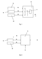
- Shown in fig. 1 are a signal acquisition device 10 and the devices supplying inputs to the signal acquisition device 10.
- the signal acquisition device 10 receives an input signal 12, a physical data 16 and a timing data 20 to generate an output data 24.
- the output data 24 is stored in the storage means 11 or sent out to other devices.
- the input signal 12 is provided by a sensor module 14.
- the input signal 12 is a binary signal having two states; a 0 or a 1.
- the input signal 12 is used as trigger to acquire the physical data 16, the timing data 20 and the state of the input signal 12 by the signal acquisition device 10.
- a rising edge and/or a falling edge of the input signal 12 can be used to acquire the data.
- the physical data 16 is provided by the physical data processing module 18.
- the physical data 16 may be any physical value like angle, length unit, temperature, voltage, pressure, and mass, current etc.
- the physical data processing module 18 can be realized as a free running counter, which counts pulses generated by a DPLL (not shown) by processing arbitrary sensor data events. There is also the possibility to process the output data (24) for this reason in the DPLL and count the output pulses of the DPLL in the physical data processing unit 18.
- the timing data 20 is provided by the timing module 22.
- the timing module 22 receives the system clock which is not shown in the figure.
- the timing module 22 is a free running counter which counts the system clock pulses from 0 to the maximum value limited by the number of counting elements. Once the counter reaches the maximum value, it starts counting again from 0.
- the signal acquisition device 10 can be configured to acquire the data with the rising edge and/or the falling edge of the input signal 12.
- the edge with which the data needs to be acquired is referred as a valid edge.
- the signal acquisition device 10 keeps monitoring the input signal 12 for a valid edge to acquire the data. Once it detects a valid edge, the signal acquisition device 10 reads the physical data 16 and the timing data 20 and generates the output data 24 which comprises the new state of the input signal 12, the physical data 16 and the timing data 20.
- the output data is also written into the storage means.
- the input signal 12 and the physical data 16 are stored along with the timing data 20 which acts as an extended time stamping; this means that not only the actual timing data but also the actual physical data at the valid edge of the input signal are recorded together with the input signal state.
- the signal acquisition device 10 also sends out the output data 24. Any device which needs to analyse the physical data with respect to the input signal 12 and the timing data 20 can receive the output signal 24 and carry on the analysis.
- the output data 24 can be in the form of a serial data or a parallel data.
- the output data 24 can go to CPU or any other devices.
- the signal acquisition device 10 keeps generating the output data 24 for every valid edge of the input signal 12.
- the output data is stored and overwritten for every new valid edge, if the time between valid edges is sufficient for further processing by following modules. Also the output data can be stored in the storage means depending upon the capacity of the storage means.
- the type and the way of generating the output data 24 by arranging the input signal 12, the physical data 16 and the timing data 20 as well as the state of the input signal 12 that should be reacted to is configurable. There may be more than one input signal; the physical data and the timing data may have to be acquired with respect to a particular input signal. As the signal acquisition device 10 supplies the extended time stamped data, the load on the other devices to read the input signal, the physical data and the timing data, is reduced and all data are brought in a context together.
- a further advantage of the aforementioned circuit is that not only the input signal 12 is time stamped using the timing data 20 but also the physical data 16 at the time when the input signal 12 was detected as valid, is time stamped using the timing data 20.
- the device can be used, for example, for signal acquisition to control an engine.
- Knowledge about the position of the pistons in the combustion cylinder along with the current system time plays an important role in the engine control.
- the engine position is determined through the position of the crankshaft.
- there is a crankshaft sensor that generates a crankshaft position signal based on the teeth of the crankshaft tone wheel which move past it.
- the crankshaft position signal is a low resolution signal, for example, if there are 60 teeth on the crankshaft tone wheel, each pulse represents 6 degrees.
- the angle information is computed by a DPLL based on the previous crank shaft position signal measurements.
- the crankshaft position signal is given as input signal 12 and the angle information is given as the physical data value (e.g.
- angle clock 16 16 to the signal acquisition device 10.
- the system clock is given as input to the timing module 22.
- the data acquisition device 10 keeps monitoring the valid edge on the input signal 12. Once a valid edge is detected, data acquisition device 10 reads the system time from the timing module, the angle information from the angle module and generates the output data. With the output data 24, it can be analysed how the angle information is behaving with respect to the system time.
- Shown in fig. 2 is another embodiment of the invention.
- the signal acquisition device 10 receives a time stamped and physical value stamped signal 50.
- the physical value stamped signal refers to a signal which has a physical value assigned to it in the same sense as time stamping i.e. a signal value and a physical value assigned to the signal value.
- the time stamped and physical stamped value signal 50 comprises an event signal, a physical event data and a time event data for generation of the event.
- the signal acquisition device 10 keeps comparing the physical event data with physical data 16 from the physical data processing module 18 and the time event data with the timing data 20 from the timing module 22. When one or both the comparisons match, the signal generation unit delivers the event signal from the physical and time stamped signal 50 as the valid output signal 54.
- the data generation device 10 can receive the time stamped signal directly from the CPU over the bus interface 52.
Abstract
The invention relates to a signal acquisition device (10) which receives an input signal (12), a physical data (16) and a timing data (20) to generate an output data (24). The signal acquisition device (10) keeps monitoring the input signal (12) for a valid edge. When a valid edge is detected, the signal acquisition device (10) reads the physical data (16) from a physical data processing module (18) and a timing data (20) from a timing module (22) to generate the output data (24) which comprises the new state of the input signal (12), the physical data (16) and the timing data (20). The output data (24) is written to a storage means (11) and also sent out to CPU or any other devices.
Description
- The invention relates to a signal acquisition device which receives different signals as inputs and generates an output data comprising all the inputs at a given instance which is triggered by change of state of one of the input signals. An
US patent 7,257,396 discloses a system and a method for collecting, storing and time-stamping telematics data. A programmable logic control unit is described that is connected to one or more sensors mounted on a vehicle to capture, time-stamp and store telematics data. And, upon the happening of a triggering event, time-stamped telematics data is transferred from the control unit to an external device. - The device according to the independent patent claim has the below mentioned advantages:
- Supplying the output data which comprises the physical data and the timing data along with the new state of the input signal provides an opportunity to analyse the physical data and the timing data to determine the behaviour of the physical value at a specific instance of time and the input signal value (or the new state of the input signal) when the input signal changed state either from 0 to 1 or 1 to 0.
- Also as the output data contains the new state of the input signal, the physical data and the timing data together, the load on the other devices to read the physical data and the timing data separately whenever the input signal changes state, is reduced. In addition the context between the physical data and timing data and the input signal value is provided by the composition of all three. The signal acquisition device provides the combined output data to other devices.
- Further improvements and/or advantages are realised by the features of the dependent patent claims.
- The signal acquisition device provides output data in serial format as well as parallel format which needs simple hardware interface with other devices.
- Brief descriptions of the drawings:
-
Figure 1 Shows the signal acquisition device according to a first embodiment -
Figure 2 Shows the signal acquisition device according to a second embodiment - Shown in
fig. 1 are asignal acquisition device 10 and the devices supplying inputs to thesignal acquisition device 10. Thesignal acquisition device 10 receives aninput signal 12, aphysical data 16 and atiming data 20 to generate anoutput data 24. Theoutput data 24 is stored in the storage means 11 or sent out to other devices. - The
input signal 12 is provided by asensor module 14. Theinput signal 12 is a binary signal having two states; a 0 or a 1. Theinput signal 12 is used as trigger to acquire thephysical data 16, thetiming data 20 and the state of theinput signal 12 by thesignal acquisition device 10. A rising edge and/or a falling edge of theinput signal 12 can be used to acquire the data. - The
physical data 16 is provided by the physicaldata processing module 18. Thephysical data 16 may be any physical value like angle, length unit, temperature, voltage, pressure, and mass, current etc. The physicaldata processing module 18 can be realized as a free running counter, which counts pulses generated by a DPLL (not shown) by processing arbitrary sensor data events. There is also the possibility to process the output data (24) for this reason in the DPLL and count the output pulses of the DPLL in the physicaldata processing unit 18. - The
timing data 20 is provided by thetiming module 22. Thetiming module 22 receives the system clock which is not shown in the figure. Thetiming module 22 is a free running counter which counts the system clock pulses from 0 to the maximum value limited by the number of counting elements. Once the counter reaches the maximum value, it starts counting again from 0. - The
signal acquisition device 10 can be configured to acquire the data with the rising edge and/or the falling edge of theinput signal 12. The edge with which the data needs to be acquired is referred as a valid edge. Thesignal acquisition device 10 keeps monitoring theinput signal 12 for a valid edge to acquire the data. Once it detects a valid edge, thesignal acquisition device 10 reads thephysical data 16 and thetiming data 20 and generates theoutput data 24 which comprises the new state of theinput signal 12, thephysical data 16 and thetiming data 20. The output data is also written into the storage means. Thus, theinput signal 12 and thephysical data 16 are stored along with thetiming data 20 which acts as an extended time stamping; this means that not only the actual timing data but also the actual physical data at the valid edge of the input signal are recorded together with the input signal state. Thesignal acquisition device 10 also sends out theoutput data 24. Any device which needs to analyse the physical data with respect to theinput signal 12 and thetiming data 20 can receive theoutput signal 24 and carry on the analysis. - The
output data 24 can be in the form of a serial data or a parallel data. Theoutput data 24 can go to CPU or any other devices. - The
signal acquisition device 10 keeps generating theoutput data 24 for every valid edge of theinput signal 12. The output data is stored and overwritten for every new valid edge, if the time between valid edges is sufficient for further processing by following modules. Also the output data can be stored in the storage means depending upon the capacity of the storage means. - The type and the way of generating the
output data 24 by arranging theinput signal 12, thephysical data 16 and thetiming data 20 as well as the state of theinput signal 12 that should be reacted to is configurable. There may be more than one input signal; the physical data and the timing data may have to be acquired with respect to a particular input signal. As thesignal acquisition device 10 supplies the extended time stamped data, the load on the other devices to read the input signal, the physical data and the timing data, is reduced and all data are brought in a context together. - A further advantage of the aforementioned circuit is that not only the
input signal 12 is time stamped using thetiming data 20 but also thephysical data 16 at the time when theinput signal 12 was detected as valid, is time stamped using thetiming data 20. - The device can be used, for example, for signal acquisition to control an engine. Knowledge about the position of the pistons in the combustion cylinder along with the current system time plays an important role in the engine control. The engine position is determined through the position of the crankshaft. For this, there is a crankshaft sensor that generates a crankshaft position signal based on the teeth of the crankshaft tone wheel which move past it. Normally the crankshaft position signal is a low resolution signal, for example, if there are 60 teeth on the crankshaft tone wheel, each pulse represents 6 degrees. The angle information is computed by a DPLL based on the previous crank shaft position signal measurements. The crankshaft position signal is given as
input signal 12 and the angle information is given as the physical data value (e.g. angle clock) 16 to thesignal acquisition device 10. The system clock is given as input to thetiming module 22. Thedata acquisition device 10 keeps monitoring the valid edge on theinput signal 12. Once a valid edge is detected,data acquisition device 10 reads the system time from the timing module, the angle information from the angle module and generates the output data. With theoutput data 24, it can be analysed how the angle information is behaving with respect to the system time. - Shown in
fig. 2 is another embodiment of the invention. Here thesignal acquisition device 10 receives a time stamped and physical value stampedsignal 50. The physical value stamped signal refers to a signal which has a physical value assigned to it in the same sense as time stamping i.e. a signal value and a physical value assigned to the signal value. The time stamped and physical stampedvalue signal 50 comprises an event signal, a physical event data and a time event data for generation of the event. Thesignal acquisition device 10 keeps comparing the physical event data withphysical data 16 from the physicaldata processing module 18 and the time event data with thetiming data 20 from thetiming module 22. When one or both the comparisons match, the signal generation unit delivers the event signal from the physical and time stampedsignal 50 as thevalid output signal 54. Here thedata generation device 10 can receive the time stamped signal directly from the CPU over thebus interface 52.
Claims (9)
- A signal acquisition device (10) comprising a storage means, the said signal acquisition unit 10 adapted to receive an input signal (12) from a sensor module (14), a physical data (16) from a physical data processing module (18), a timing data (20) from a timing module (22) to generate an output data (24) comprising the new state of the input signal which is either high or a low, the physical data (16) and the timing data (20).
- A signal acquisition device (10) according to claim 1 wherein the new state of the said input signal (12), the said physical data (16) and the said timing data (18) are stored in the storage means (11) when a valid edge is detected on the input signal (12).
- A signal acquisition device (10) according to claim 1 and 2 wherein the valid edge of the input signal is configurable as from 0 to 1 and/or from 1 to 0 levels.
- A signal acquisition device (10) according to claim 1 wherein the said output data (24) is a serial data.
- A signal acquisition device (10) according to claim 1 wherein the said output data (24) is a parallel data.
- A signal acquisition device (10) according to claim 1 wherein the said input data (12) is a crankshaft data of a combustion engine.
- A signal acquisition device (10) according to claim 1 wherein the said signal acquisition unit receives a time stamped and physical value stamped signal 50 comprising an event signal, a physical event data and a time event data.
- A signal acquisition device (10) according to claim 1 and 7 wherein the said signal acquisition device (10) compares the physical event data with the physical data 16 from the physical data processing module 18 and compares the time event data with the timing data 20 from the timer module 22; and when one or both the comparisons match, the signal acquisition unit (10) provides the event signal at the output 54.
- A method to generate a data signal, the said method comprising the steps:- receiving an input signal (12), a physical data (16) and a timing data (20)- generating the output data (24) comprising the new state of the input signal (12), the physical data (16) and the timing data (20) when a valid edge is detected on the input signal (12)- storing the output data (24) in a storage means (11) and also sending the output data (24) to other devices.
Priority Applications (3)
| Application Number | Priority Date | Filing Date | Title |
|---|---|---|---|
| EP09166984A EP2282296A1 (en) | 2009-07-31 | 2009-07-31 | A signal acquisition device |
| US12/839,508 US20110029284A1 (en) | 2009-07-31 | 2010-07-20 | Signal acquisition device |
| CN2010102432035A CN101989306A (en) | 2009-07-31 | 2010-07-30 | A signal acquisition device |
Applications Claiming Priority (1)
| Application Number | Priority Date | Filing Date | Title |
|---|---|---|---|
| EP09166984A EP2282296A1 (en) | 2009-07-31 | 2009-07-31 | A signal acquisition device |
Publications (1)
| Publication Number | Publication Date |
|---|---|
| EP2282296A1 true EP2282296A1 (en) | 2011-02-09 |
Family
ID=41278883
Family Applications (1)
| Application Number | Title | Priority Date | Filing Date |
|---|---|---|---|
| EP09166984A Withdrawn EP2282296A1 (en) | 2009-07-31 | 2009-07-31 | A signal acquisition device |
Country Status (3)
| Country | Link |
|---|---|
| US (1) | US20110029284A1 (en) |
| EP (1) | EP2282296A1 (en) |
| CN (1) | CN101989306A (en) |
Families Citing this family (1)
| Publication number | Priority date | Publication date | Assignee | Title |
|---|---|---|---|---|
| KR101855523B1 (en) * | 2011-10-06 | 2018-05-04 | 삼성전자주식회사 | Method and device of generating feedback in a communication system |
Citations (4)
| Publication number | Priority date | Publication date | Assignee | Title |
|---|---|---|---|---|
| US7257396B2 (en) | 2002-03-21 | 2007-08-14 | United Parcel Service Of America, Inc. | Telematic programming logic control unit and methods of use |
| DE102006008637A1 (en) | 2006-02-24 | 2007-08-30 | Robert Bosch Gmbh | Passenger protection system for vehicle, has activating data memory storing detected activating-relevant data that is combined with auxiliary data from positioning and/or navigation system in case of activating passenger protection device |
| US20070299992A1 (en) * | 2006-06-23 | 2007-12-27 | Fujitsu Ten Limited | Signal processing device |
| US20080319604A1 (en) | 2007-06-22 | 2008-12-25 | Todd Follmer | System and Method for Naming, Filtering, and Recall of Remotely Monitored Event Data |
Family Cites Families (8)
| Publication number | Priority date | Publication date | Assignee | Title |
|---|---|---|---|---|
| JPS58133481A (en) * | 1982-02-03 | 1983-08-09 | Nissan Motor Co Ltd | Timing sensing device of internal-combustion engine |
| FR2621433B1 (en) * | 1987-10-06 | 1989-12-08 | Thomson Semiconducteurs | METHOD FOR EXPANSION OF AN ANALOGUE SIGNAL AND DEVICE FOR IMPLEMENTING THE METHOD |
| EP0587093B1 (en) * | 1992-09-08 | 1999-11-24 | Hitachi, Ltd. | Information processing apparatus using inference and adaptive learning |
| US6532936B1 (en) * | 2001-10-30 | 2003-03-18 | Delphi Technologies, Inc. | System and method for altering engine ignition timing |
| WO2004109704A1 (en) * | 2003-06-05 | 2004-12-16 | Koninklijke Philips Electronics N.V. | Integrity control for data stored in a non-volatile memory |
| US20080253479A1 (en) * | 2004-04-16 | 2008-10-16 | Data Flow Technologies, Inc. | Single and multiple sinewave modulation and demodulation techniques, apparatus, and communications systems |
| DE102005060394B4 (en) * | 2005-12-16 | 2012-10-11 | Infineon Technologies Ag | Circuit arrangement and method for operating a circuit arrangement |
| US7461186B2 (en) * | 2006-02-03 | 2008-12-02 | Infineon Technologies Ag | Data handover unit for transferring data between different clock domains by parallelly reading out data bits from a plurality of storage elements |
-
2009
- 2009-07-31 EP EP09166984A patent/EP2282296A1/en not_active Withdrawn
-
2010
- 2010-07-20 US US12/839,508 patent/US20110029284A1/en not_active Abandoned
- 2010-07-30 CN CN2010102432035A patent/CN101989306A/en active Pending
Patent Citations (4)
| Publication number | Priority date | Publication date | Assignee | Title |
|---|---|---|---|---|
| US7257396B2 (en) | 2002-03-21 | 2007-08-14 | United Parcel Service Of America, Inc. | Telematic programming logic control unit and methods of use |
| DE102006008637A1 (en) | 2006-02-24 | 2007-08-30 | Robert Bosch Gmbh | Passenger protection system for vehicle, has activating data memory storing detected activating-relevant data that is combined with auxiliary data from positioning and/or navigation system in case of activating passenger protection device |
| US20070299992A1 (en) * | 2006-06-23 | 2007-12-27 | Fujitsu Ten Limited | Signal processing device |
| US20080319604A1 (en) | 2007-06-22 | 2008-12-25 | Todd Follmer | System and Method for Naming, Filtering, and Recall of Remotely Monitored Event Data |
Also Published As
| Publication number | Publication date |
|---|---|
| CN101989306A (en) | 2011-03-23 |
| US20110029284A1 (en) | 2011-02-03 |
Similar Documents
| Publication | Publication Date | Title |
|---|---|---|
| US7619560B2 (en) | GPS processing arrangement | |
| EP2965458B1 (en) | Dithering circuit for sampling serial data transmission | |
| WO2005062181A1 (en) | Apparatus and method for time ordering events in a system having multiple time domains | |
| EP2770489A1 (en) | Data recording device for vehicle | |
| EP4057513A1 (en) | Sensor data processing for condition monitoring systems | |
| GB2428826A (en) | Timestamp generator with precision recording | |
| TWI598572B (en) | Sensor and process to assign time information to sensed measurement data of a sensor | |
| DE102010000962A1 (en) | Method and device for monitoring a frequency signal | |
| CN107637091A (en) | The method and apparatus synchronous for sensor | |
| US7827377B2 (en) | Method for reading out sensor data | |
| EP2282296A1 (en) | A signal acquisition device | |
| US8706981B2 (en) | Configurable status processing unit for sensor-actuator systems | |
| US10320407B1 (en) | Low power synchronization of multiple analog to digital converters | |
| EP3367706B2 (en) | A method, a network node and a system for triggering a transmission of sensor data from a wireless device | |
| JP5078276B2 (en) | Diagnostic signal processor | |
| JP2003285700A (en) | Failure-diagnosing device for vehicle | |
| CN101093403B (en) | Method for reducing electromagnetic interference of clock circuit and clock management circuit | |
| US8775852B2 (en) | Method for sensing input signal changes | |
| JP2015005124A (en) | Device for electronic apparatus, and electronic apparatus mounting the device therein | |
| JP5294138B2 (en) | Pulse output device | |
| EP3931580B1 (en) | Method and evaluation unit for determining a time of a flank in a signal | |
| JP2018200570A (en) | Bus monitor and bus monitoring method | |
| JP4451603B2 (en) | Fault detection method for members | |
| US7417571B2 (en) | Method for providing a correlation | |
| EP2727523A2 (en) | Electronic device, method of extracting data and program |
Legal Events
| Date | Code | Title | Description |
|---|---|---|---|
| PUAI | Public reference made under article 153(3) epc to a published international application that has entered the european phase |
Free format text: ORIGINAL CODE: 0009012 |
|
| AK | Designated contracting states |
Kind code of ref document: A1 Designated state(s): AT BE BG CH CY CZ DE DK EE ES FI FR GB GR HR HU IE IS IT LI LT LU LV MC MK MT NL NO PL PT RO SE SI SK SM TR |
|
| AX | Request for extension of the european patent |
Extension state: AL BA RS |
|
| 17P | Request for examination filed |
Effective date: 20110809 |
|
| 17Q | First examination report despatched |
Effective date: 20111006 |
|
| STAA | Information on the status of an ep patent application or granted ep patent |
Free format text: STATUS: THE APPLICATION IS DEEMED TO BE WITHDRAWN |
|
| 18D | Application deemed to be withdrawn |
Effective date: 20140415 |