EP2282266A1 - Index cache tree - Google Patents
Index cache tree Download PDFInfo
- Publication number
- EP2282266A1 EP2282266A1 EP20100170699 EP10170699A EP2282266A1 EP 2282266 A1 EP2282266 A1 EP 2282266A1 EP 20100170699 EP20100170699 EP 20100170699 EP 10170699 A EP10170699 A EP 10170699A EP 2282266 A1 EP2282266 A1 EP 2282266A1
- Authority
- EP
- European Patent Office
- Prior art keywords
- entry
- logical address
- volatile memory
- address
- index
- Prior art date
- Legal status (The legal status is an assumption and is not a legal conclusion. Google has not performed a legal analysis and makes no representation as to the accuracy of the status listed.)
- Withdrawn
Links
Images



Classifications
-
- G—PHYSICS
- G06—COMPUTING OR CALCULATING; COUNTING
- G06F—ELECTRIC DIGITAL DATA PROCESSING
- G06F12/00—Accessing, addressing or allocating within memory systems or architectures
- G06F12/02—Addressing or allocation; Relocation
- G06F12/08—Addressing or allocation; Relocation in hierarchically structured memory systems, e.g. virtual memory systems
- G06F12/10—Address translation
- G06F12/1009—Address translation using page tables, e.g. page table structures
-
- G—PHYSICS
- G06—COMPUTING OR CALCULATING; COUNTING
- G06F—ELECTRIC DIGITAL DATA PROCESSING
- G06F12/00—Accessing, addressing or allocating within memory systems or architectures
- G06F12/02—Addressing or allocation; Relocation
- G06F12/08—Addressing or allocation; Relocation in hierarchically structured memory systems, e.g. virtual memory systems
-
- G—PHYSICS
- G06—COMPUTING OR CALCULATING; COUNTING
- G06F—ELECTRIC DIGITAL DATA PROCESSING
- G06F12/00—Accessing, addressing or allocating within memory systems or architectures
- G06F12/02—Addressing or allocation; Relocation
- G06F12/0223—User address space allocation, e.g. contiguous or non contiguous base addressing
- G06F12/023—Free address space management
- G06F12/0238—Memory management in non-volatile memory, e.g. resistive RAM or ferroelectric memory
- G06F12/0246—Memory management in non-volatile memory, e.g. resistive RAM or ferroelectric memory in block erasable memory, e.g. flash memory
-
- G—PHYSICS
- G06—COMPUTING OR CALCULATING; COUNTING
- G06F—ELECTRIC DIGITAL DATA PROCESSING
- G06F12/00—Accessing, addressing or allocating within memory systems or architectures
- G06F12/02—Addressing or allocation; Relocation
- G06F12/06—Addressing a physical block of locations, e.g. base addressing, module addressing, memory dedication
-
- G—PHYSICS
- G06—COMPUTING OR CALCULATING; COUNTING
- G06F—ELECTRIC DIGITAL DATA PROCESSING
- G06F2212/00—Indexing scheme relating to accessing, addressing or allocation within memory systems or architectures
- G06F2212/72—Details relating to flash memory management
- G06F2212/7201—Logical to physical mapping or translation of blocks or pages
Definitions
- This subject matter is generally related to memory mapping.
- Flash memory is a type of electrically erasable programmable read-only memory (EEPROM). Because flash memories are non-volatile and relatively dense, they are used to store files and other persistent objects in handheld computers, mobile phones, digital cameras, portable music players, and many other devices in which other storage solutions (e.g., magnetic disks) are inappropriate. Unfortunately, flash suffers from two limitations. First, bits can only be cleared by erasing a large block of memory. Second, each block can only sustain a limited number of erasures, after which it can no longer reliably store data. Due to these limitations, complex data structures and algorithms are often required to effectively use flash memories. These algorithms and data structures are used to support efficient not-in-place updates of data, reduce the number of erasures, and level the wear of the blocks in the device.
- EEPROM electrically erasable programmable read-only memory
- Flash memories do not support in-place updates or rewrites to physical memory pages unless the block containing the page is erased first.
- a hardware and/or software layer is often added to the flash subsystem.
- This layer often referred to as a flash translation layer (FTL)
- FTL flash translation layer
- the FTL is implemented as a controller in hardware.
- the controller can include a processor or microcontroller along with small amounts of volatile memory (e.g., RAM).
- the controller can be responsible for translating a read/write request from the file system (e.g., a logical sector) into a read/write operation on a specific block of flash.
- the controller can attempt to resolve the mapping of logical sectors to physical memory pages.
- a memory mapping technique for non-volatile memory where logical sectors are mapped into physical pages using data structures in volatile and non-volatile memory.
- a first lookup table in non-volatile memory maps logical sectors directly into physical pages.
- a second lookup table in volatile memory holds the location of the first lookup table in non-volatile memory.
- An index cache tree in volatile memory holds the physical addresses of the most recently written or accessed logical sectors in a compressed format.
- the disclosed memory mapping techniques provide several advantages over conventional flash memory block mapping techniques. Some of these advantages include but are not limited to: 1) eliminating the need for block mapping by directly mapping logical sectors to physical pages, 2) eliminating the need for allocating new blocks until all pages in a current block are allocated, 3) eliminating the need for allocating different journaling blocks for different logical areas, and 4) eliminating the need for triggering a garbage collection operation until all pages in the current block are allocated. Additional advantages associated with using the disclosed index cache tree data structure in volatile memory can include but are not limited to: 1) increasing a number of logical sectors that are mapped to physical addresses in volatile memory, and 2) decreasing that average time it takes the controller to resolve a logical sector to a physical address.
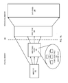
- FIG. 1A is a block diagram illustrating an example memory mapping architecture for mapping logical sectors into physical pages using a lookup table and an index cache tree.
- FIGS. 1B-1C are block diagrams illustrating example mappings of logical sectors directly into physical data pages using an example index cache tree.
- FIGS. 2A-2B are flow diagrams of an example read operation using the memory mapping architecture shown in FIGS. 1A-1C .
- FIGS. 3A-3B are flow diagrams of an example operation for locating an entry in an index cache tree using the memory mapping architecture of FIGS. 1A-1C .
- FIG. 4 is a flow diagram of an example operation for adding an entry to an index cache tree using the memory mapping architecture of FIGS. 1A-1C .
- FIG. 5A is a block diagram of example memory subsystem for implementing the memory architecture and operations of FIGS. 1-4 .
- FIG. 5B is a block diagram illustrating the system architecture of an example device including a memory subsystem for implementing the memory architecture and operations of FIGS. 1-4 .
- FIG. 1A is a block diagram illustrating an example memory mapping architecture 100 for mapping logical sectors into physical pages using a lookup table and an index cache tree.
- a lookup table 102 in volatile memory e.g., RAM
- the lookup table 106 holds the physical addresses of data pages 108.
- a cache 104 in volatile memory holds the physical addresses of recently written, read, or accessed logical sectors to allow faster readout.
- the lookup table 102 is also referred to as a index TOC 102
- the lookup table 106 is also referred to as the index table 106 or index page
- the cache 104 is also referred to as the index table cache 104.
- the index TOC 102 and the index table cache 104 enable at least a portion of the index table 106 to be stored in the non-volatile memory. This is advantageous since the small amount of RAM that is typically available in controllers cannot be scaled due to a rise in cost, area and power consumption of the controller.
- the volatile memory can be dynamically configured based on its availability or other trigger events and/or operational modes.
- the index cache table 104 includes an index cache tree data structure 110.
- the index cache tree data structure 110 is also referred to as the index cache tree 110.
- the index cache tree 110 uses a tree structure (e.g., a b-tree, a b*-tree, etc.) to decrease the retrieval time for entries within the index table cache 104.
- a data structure that enables efficient searching (e.g., binary search, etc.) of entries contained in the index table cache 104
- increased speed can be gained when determining whether a desired logical to physical address mapping is contained within the index table cache 104.
- the more quickly a determination as to whether a logical to physical address mapping is contained within the index table cache 104 the sooner a flash memory device employing the architecture 100 can either use the mapping to initiate retrieval of the identified physical memory. This is advantageous since a flash memory device may consult the index table cache 104 frequently (e.g., during read operations) when attempting to resolve a logical to physical address mapping.
- the index cache tree 110 can also use data compression to increase the storage capacity of the index cache table 104.
- By increasing the capacity of the index table cache 104 to store logical to physical address mappings a flash memory device employing the architecture 100 will more frequently locate a desired mapping within the index cache table 104 and less frequently have to initiate retrieval of a desired mapping from the index table 106 in non-volatile memory. This is advantageous since retrieval from the index table cache 104 in volatile memory will generally be faster than retrieval from the index table 106 in non-volatile memory.
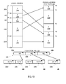
- FIG. 1B is a block diagram illustrating an example mapping of logical sectors directly into physical data pages 119 using an example index cache tree 118.
- the index cache tree 118 is similar to the index cache tree 110 and the data pages 119 are similar to the data pages 108, as described above with regard to FIG. 1A .
- the index cache tree 118 has a tree structure that uses two levels of data compression. The first level of data compression corresponds to run-length encoding and the second level of data compression corresponds to a flag designating a size for each entry in the tree. The entry size can correspond to a number of bits allocated to the run-length encoding span.
- a flag can indicate which of a fixed number of predetermined sizes correspond to each entry. For instance, if a device generally stores small files (e.g., text files, configuration files, etc.) and large files (e.g., audio files, video files, etc.), the flag can indicate which of two fixed sizes (e.g., 4-bits and 6-bits) are used for run-length encoding each entry.
- predetermined entry sizes e.g., two sizes, four sizes, eight sizes, ten sizes, etc.
- variable-sized entries for storing a physical address and/or pointer fields can be used.
- the data files A-E 120a-e are illustrated as corresponding to logical addresses.
- data file B 120b is depicted as corresponding to address 300.
- the size of each of the data files, A-E 120a-e, is shown by the numbered spans to the left of the data files A-E 120a-e.
- the data file D 120d has a logical address span of 400.
- the data files A-E 120a-e correspond to physical locations in the data pages 119, as depicted by physical data files A-E 122a-e.
- Each of these physical data files A-E 122a-e has a corresponding physical address P0-P4.
- the physical data file A 122a has the physical address P2.
- Index cache tree 118 maps the logical addresses to the physical addresses using tree of nodes 124, 128, 132, and 136.
- Each of the nodes 124, 128, 132, and 136 contains at least one of the entries 126a-c, 130a-b, 134a-b, and 138a.
- the entries are populated with logical address spans for each of the data files A-E 120a-e and either a pointer to another node or a physical address for a corresponding physical data file A-E 122a-e.
- the entry 130a corresponding to data file A 120a contains the logical address span 300 and the physical address P2 of the physical data file A 122a.
- a logical address offset can be the difference between the logical address of an entry and the first logical address.
- the nodes 124, 128, 132, and 136 and the entries 126a-c, 130a-b, 134a-b, and 138a are arranged left-to-right from the smallest logical address offset to the greatest logical address offset. For instance, since the entry 130a corresponds to data file A 120a (having logical address 0) and the entry 130b corresponds to the data file B 120b (having logical address 300), the entry 130a is arranged to the left of the entry 130b.
- the logical address offset for a data file can be used to locate the physical address for the data file.
- the logical address spans stored in the entries 126a-c, 130a-b, 134a-b, and 138a are aggregated as the nodes 124, 128, 132, and 136 are traversed.
- the aggregated value (e.g., a tally) serves as the logical address offset for the entry that is currently being evaluated.
- the tally is initialized at zero and traversal of the index cache tree 118 can begin with the first entry 126a (e.g., the entry with the smallest logical address offset) of the root node 124. If the logical address offset at issue (e.g., logical address for which a physical address is sought) is greater than or equal to the tally plus the logical address span of the entry being evaluated, then the logical address span of the entry is added to the tally and the next entry in the node is evaluated.
- the logical address offset at issue e.g., logical address for which a physical address is sought
- the entry being evaluated corresponds to the logical address offset at issue. In such a case, if the entry being evaluated stores a pointer to another node, then evaluation shifts to the first entry of the pointed to node. If the entry being evaluated stores a physical address, then evaluation can end because the corresponding physical address has been located.
- each entry in the index cache tree 118 is compressed.
- the logical address span will generally be a fraction of the size of the logical address, allowing fewer bits to be allocated.
- the index table cache 104 can store a greater number of entries using the index cache tree 118, which can in-turn improve the speed by which memory accesses are processed and create greater efficiency within a flash memory device.
- the description above regarding using the logical address span corresponds to the first level of data compression within the index cache tree 118.
- the second level of data compression regards a flag contained in each entry that indicates a length type for the entry.
- the flag (represented by the box in the upper-right corner of each entry) indicates whether an entry is a short entry (e.g., 1 byte, 2 bytes, 4 bytes, 6 bytes, etc.) or a long entry (e.g., 2 bytes, 4 bytes, 6 bytes, 8 bytes, 10 bytes, 16 bytes, 32 bytes, etc.).
- the entries having an "X" (entries 126a-c, 130a, 134b, and 138a) are designated as long entries.
- the dashed line is intended to illustrate the additional bit-length for the long entries.
- the example above is provided for illustrative purposes. Any number of entry lengths can be used (e.g., two, four, six, eight, sixteen, etc.) -- the number of entry lengths is not limited to two entry lengths (short and long entries).
- the length type for an entry can be based upon a variety of factors, such as a bit-length for a logical address span and/or whether the entry stores a pointer or a physical address.
- the determination as to whether an entry is a short or long entry corresponds to the length of logical address span.
- the entries storing three digit logical address spans e.g., logical address span 300 for entry 130a
- the entries storing two digit logical address spans e.g., logical address span 40 for entry 130b
- the number of bits for each length type and the number of length types can vary depending on a variety of factors. Such factors can include an intended use for the flash memory device (e.g., portable media player, thumb drive, smart phone, embedded device, etc.), usage statistics for the device (e.g., file type accessed most frequently, common file lengths, etc.), available space in the index table cache 104 for the index cache tree 118, etc.
- a smart phone that stores contact information, emails, text messages, and media files may be configured to have four length types that are tailored to these four common types of files.
- the number of bits for each length type and/or the number of length types can additionally vary over the lifetime of a device. For example, on power-up the device may evaluate usage statistics for the device to determine whether an adjustment to the present scheme should be made.
- Use of the flag indicated length types for entries in the index cache tree 118 provides an additional level of compression that can enable the index table cache 104 to store more of the index table 106 from non-volatile memory. As articulated above, the more entries that are stored within the index table cache 104, the faster the flash memory device will be able to obtain the physical address on average. Additionally, bit usage efficiency can be increased. For instance, by using a flag to indicate the length, the occurrence of unused bits is minimized (e.g., the extra bits associated with a long entry are only allocated when needed) with a minimal number of bits being dedicated to identifying a length for each entry.
- FIG. 1C is a block diagram illustrating another example mapping of logical sectors directly into physical data pages 149 using an example index cache tree 148.
- the index cache tree 148 is similar to the index cache trees 110 and 118, and the data pages 149 are similar to the data pages 108 and 119, as described above with regard to FIGS. 1A-1B .
- the depicted example index cache tree 148 demonstrates fixed size nodes, multi-tiered nodes, a file in the data pages 149 that is not listed in the index cache tree, gaps in the logical address offset sequence in index cache tree 148, and nodes having mixed entries with pointers and physical addresses.
- the data pages 149 include multiple files A-ZZ 150a-h, each of which has a physical address. Similar to the index cache tree 118, the index cache tree 148 contains multiple nodes 152-166 and multiple entries 152a-d, 154a-e, 156a-c, 158a-d, 160a-f, 162a-d, 164a-c, and 166a-e.
- long entries e.g., entry 152b
- short entries e.g., entry 152a
- the short entries are intended to be approximately half the length of the long entries (e.g., half the number of bits).
- any ratio of short to long entries e.g., 4-bytes to 6-bytes, etc.
- any number of entry lengths can be used (e.g., 4 different entry lengths could be used).
- the entries that contain a file 150a-h letter are intended to be representative of storing a physical address for the identified file.
- logical page spans can also be present within each entry, similar to the description regarding logical page spans above with regard to FIG. 1B .
- index cache tree 148 demonstrates fixed size nodes, which means that each node is allocated the same amount of memory space within an index cache (e.g., index table cache 104).
- each of the nodes 152-166 contains the same total length of entries (e.g., node 156 contains three long entries 156a-c, which in this example is the equivalent of the six short entries 160a-f contained in node 160).
- the amount of memory allocated for each node can be based on the spacing of data lines within a cache (e.g., each node can be allocated 24 bytes, 32 bytes, 64 bytes, 128 bytes, 512 bytes, 1024 bytes, etc.), or other alignments for volatile memory access efficiency.
- Such fixed memory allocation for each node can be cached memory that is used and divided efficiently.
- the nodes 152-166 are multi-tiered.
- the node 152 has an entry 152b that points to the node 156, which in-turn has a node 156c that points to the node 164.
- Various node and element balancing and re-packaging techniques can be used to ensure optimal distribution of nodes and entries across the index cache tree 148.
- each node can be mixed between storing a pointer and a physical address.
- the node 158 contains three entries 158a-b and 158d that contain physical addresses and one entry 158c that contains a pointer.
- the index cache tree 148 may not contain sufficient storage capacity to represent all of the logical address to physical address mappings contained in an index table in non-volatile memory (e.g., index table 106). For example, the file D 150d is not contained in the index cache tree 148.
- the index cache tree 148 can contain gaps in the linear logical address offset that are represented by the entries. Such gaps can be represented by entries that contain a logical address span but do not contain a pointer or a physical page address (e.g., entries 164b and 166c). In such instances, the gap may cover the logical address offset for several files. For example, the entry 164b may cover the logical address offset corresponding to file D 150d and a file F (not depicted). Were a request for the logical to physical address mapping of the file D 150d to be received, then the entry 164b could be replaced, at least in part, with an entry corresponding to the file D 150d. Given the fixed size nature of the node 164, insertion of an entry corresponding to the file D 150d can result in deletion of another entry and/or node.
- each entry of the index TOC 102 stores a physical address in non-volatile memory of an index table 106 entry and a pointer to an entry in the index table cache 104.
- the address 0xff or other suitable indicator can be placed in a index TOC 102 entry to indicate that a desired index table 106 entry is not stored in the index table cache 104.
- the index table 106 can include a flat file structure that provides the logical address to physical address mappings. In other implementations, the index table 106 can include an index tree that provides compression of data entries, similar to the index cache trees 110, 118, and/or 148.
- each entry of the index cache tree 110 can include but is not limited to: status data (e.g., clean, dirty, free), and/or a counter (e.g., a serial counter or count indicating how many times that particular block has been accessed).
- status data e.g., clean, dirty, free
- a counter e.g., a serial counter or count indicating how many times that particular block has been accessed.
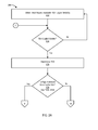
- FIGS. 2A-2B are flow diagrams of an example read operation 200 using the memory mapping architecture shown in FIGS. 1A-1C .
- the read operation 200 can begin by obtaining a read request associated with one or more logical sectors (202).
- the read request can be issued by a file system.
- the read request can include a first sector number and a number of consecutive sectors.
- an index TOC e.g., index TOC 102 in volatile memory is checked (206) to determine if a data page address associated with the current logical sector is stored in an index cache tree in volatile memory (e.g., index cache tree 110, 118, and 148). If the data page address is stored in the index cache tree (208), then the data page address is read from the index cache tree (210) and used to perform the read operation on non-volatile memory (212).
- the data page address is not stored in the index table cache (208), then the physical page address of the relevant index table entry storing the data page address is read from the index TOC (214), and the relevant index table entry storing the data page address is read from the index table entry and stored in the index table cache (216).
- the data page address can then be read from the index cache tree (210) and used to perform the read operation on non-volatile memory (212).
- step 216 if during step 216 the index cache tree is full, older data page addresses in the index cache tree can be flushed to make room for newer data page addresses read from the index table in non-volatile memory.
- the flushing of the index cache tree can trigger unnecessary write operations on non-volatile memory.
- an overflow buffer can be created in volatile memory and used to store the data page address read from the index table in non-volatile memory.
- the overflow buffer can be read to get the data page address for use in the read operation 200.
- creating an overflow buffer in volatile memory can prevent unnecessary write operations to non-volatile memory during read operations.
- the index TOC 102 in volatile memory contains information about the index table 106 that holds the physical page address of the data page 108 to be read. At least a portion of the index table 106 can be stored in the index cache tree 110 in volatile memory or stored in an index block in non-volatile memory. If the index table 106 is stored in the index cache tree 110, the index table 106 can be read from the index cache tree 110 and used to find the physical address of the data page 108 to be read in non-volatile memory. If the index table 106 is not stored in the index cache tree 110, then the data page address can be read from the relevant entry of the index table 106 in non-volatile memory and inserted into the index cache tree 110. The data page address can be read from the index cache tree 110 and used to perform the read operation on the data page 108 in non-volatile memory.
- the read operation 200 gets a logical sector number (Lpn) and a number of consecutive logical sectors to read.
- the read operation 200 maps the logical sector number into physical locations in the non-volatile memory. Assuming a page size of 2KB, some example steps for the read operation 200 can be described using pseudo code as follows:
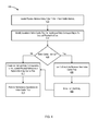
- FIGS. 3A-3B are flow diagrams of an example operations 300 for locating an entry in an index cache tree using the memory mapping architecture of FIGS. 1A-1C .
- the operation 300 can begin by locating a root node of an index cache tree (302).
- the root node 124 of the index cache tree 118 or the root node 152 of the index cache tree 148 can be located, as described with reference to FIGS. 1B-1C .
- the root node can be located in response to receiving a read request, such as at step 208 in response to the read request 202 described with regard to FIGS. 2A-2B .
- the first entry of the root node (e.g., the current node being evaluated) is identified (304).
- the first entry 126a of the root node 124 is identified.
- the logical address span for the identified entry is read and added to a tally (306).
- the tally corresponds to the logical address offset for the entry.
- the tally can be initialized before the logical address span from the identified entry is added, as described with reference to FIG. 1B .
- the logical sector such as the logical sector obtained with a read request (202), is compared against the tally (308). If the logical sector is not greater than or equal to the tally (308), then the next entry in the current node is identified (304), as described above with regard to FIG. 1B .
- the identified entry is determined to correspond to the logical sector. If the identified entry contains a physical address (310), then a read operation is performed on non-volatile memory using the physical address contained in the entry (318), such as the read operation described with regard to FIG. 2B . If the identified entry does not contain a physical address, then a determination is made as to whether the identified entry contains a pointer to another node (312). If the identified entry does have a pointer to another node, then a next node indicated by the pointer is identified (step 314).
- the first entry of the next node is identified (304), the logical address span for the identified entry is added to the tally (306), and the tally is compared to the logical sector (308), as described above with regard to FIG. 1B .
- the physical address for the logical sector can be located using the index table in non-volatile memory (e.g., index table 106) (314). Additionally, the identified physical address for the logical sector can be added as an entry to the index cache tree (e.g., index cache trees 110, 118, and 148), as describe in further detail with regard to FIG. 4 .
- the index cache tree e.g., index cache trees 110, 118, and 148
- the nodes and entries of an index cache tree can be located, added to the tally, and compared against the logical sectors until either the identified entry contains a physical address (318) or the identified entry does not contain either a physical address or a pointer to another node (316), such as entry 164b of node 164 described above with regard to FIG. 1C .
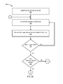
- FIG. 4 is a flow diagram of an example operation 400 for adding an entry to an index cache tree using the memory mapping architecture of FIG. 1A-1C .
- the operation 400 can be used to add an entry mapping a logical address to physical address for a logical sector that is not represented in an index cache tree.
- the operation 400 can be performed after a logical address to physical address is retrieved from non-volatile memory, such as at steps 216 and 316, as described with regard to FIGS. 2B and 3B .
- the physical address for a logical sector that is not represented in an index cache tree is located in non-volatile memory using an index table (e.g., index table 106) (402).
- a location in the index cache tree is located for inserting an entry that corresponds to the physical address located from the non-volatile memory (404).
- An operation similar to the operation 300 can be performed to locate an appropriate node and entry where the physical address located from non-volatile memory can be added.
- the appropriate location may be an entry, such as entries 164a and 166b described with regard to FIG. 1C , that contains a logical address span without a pointer or physical address.
- an entry (or possibly a node) can be identified to be removed from the index cache tree (408).
- a variety of techniques can be used to identify an entry or node to remove from the index cache tree. For instance, in some implementations the oldest entry (e.g., the least recently added to the index cache tree) is removed from the index cache tree. In other implementations the least recently accessed entry can be removed. In some implementations, the data structure may be divided into multiple trees, and the tree(s) with the highest memory usage may be removed. Information regarding the age and accesses of an entry in the index cache tree, and size of the tree(s), can be obtained from metadata associated with the index cache tree and stored in volatile memory (e.g., a counter for an entry, etc.).
- the entries (or nodes) identified to be removed from the index cache tree is erased from the index cache tree (410).
- An entry corresponding to the located physical address is created and added to a node in the index cache tree (412) at the identified location (e.g., the location identified at step 404).
- Maintenance operations are performed on the index cache tree (414). Maintenance operations can include balancing and re-packing the index cache tree so that a near even distribution of entries and nodes is achieved, and wasted space is minimized.
- logical address spans for parent entries e.g., entries that contain a pointer to another node, such as entry 126a from FIG. 1B
- a variety of tree balancing and re-packing techniques known in the art can be used.
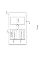
- FIG. 5A is a block diagram of example memory subsystem for implementing the memory architecture and operations of FIGS. 1-4 .
- the subsystem 500 can include a controller 502, non-volatile memory 504 and host interface 506.
- the controller 502 can include volatile memory 510 (e.g., RAM) and processor 508.
- the volatile memory 510 stores a block TOC 512, a block table 513 and an index table cache 514.
- the index table cache 514 can employ an index cache tree 515 (e.g., index cache trees 110, 118, and 148) to perform the operations described above.
- the volatile memory 510 can be configured dynamically by the processor 508 based on availability and any other suitable factors.
- the non-volatile memory 504 can include an index table 516 and data pages 518.
- the subsystem 500 can include other components that have been omitted from FIG. 5 for clarity.
- the host interface 506 can obtain read/write requests from a host system over a bus (e.g., IDE/ATT).
- the host interface 506 can include circuitry and software for receiving data, addresses and control signals.
- the read/write requests can include a logical sector number and a number of consecutive logical sectors to read/write.
- the processor 508 can access the volatile memory 510 and read the index TOC 512 to determine if the index table cache 514 includes physical addresses for the logical sector. More specifically, the processor 508 can use the index cache tree 515 (e.g., index cache trees 110, 118, and 148) to determine if the physical addresses for the logical sectors are included in the index table cache 514. If the index cache tree 515 includes the physical addresses, then the physical addresses are used for the read/write operation. If the index cache tree 515 does not include the physical addresses, then the processor 508 accesses volatile memory 510 to read the index TOC 512 to get the page address of the index table 516 in the non-volatile memory 504. The processor 508 can use the physical addresses in the index table 516 to perform a memory mapping to data pages 518 during the read/write operation.
- the index cache tree 515 e.g., index cache trees 110, 118, and 1408
- the data pages 518, index TOC 512 and/or index table 516 can be implemented on one or more different memory devices.
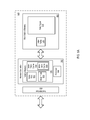
- FIG. 5B is a block diagram illustrating an example device 520 including a memory subsystem for implementing the memory architecture and operations of FIGS. 1-4 .
- the device 520 is a portable device, such as a media player device, a personal digital assistant, a mobile phone, portable computers, digital cameras, and so on, for example.
- the device 520 includes a host controller (or a so-called “System-on-Chip” or “SoC") 522 and non-volatile memory 528.
- the device 520 can optionally include additional memory external to the host controller 522 and the non-volatile memory 528.
- the host controller 522 includes one or more processors 524 and volatile memory 526.
- volatile memory 526 is static random-access memory (SRAM).
- SRAM static random-access memory
- the host controller 522 performs various processing operations and input/output operations, including the operations described in reference to FIGS. 2-4 .
- the host controller 522 can receive and process user inputs, generate outputs, perform media (e.g., audio, video, graphics) decoding and processing operations, other processing operations, and so on.
- the host controller 522 can read data from and write data to volatile memory 526.
- the host controller 522 can also issue read or write operations to the non-volatile memory 528 through an interface (not shown).
- requests for data can be issued by and/or received by the host controller 522.
- the host controller 522 can issue a request for data contained in the non-volatile memory 528.
- the issued request can be received by the host controller 522 and a logical address for the requested data can be resolved to a physical address using an index cache tree, as described above with reference to FIGS. 1-4 .
- the non-volatile memory 528 is NAND flash memory. In some other implementations, the non-volatile memory 528 is another type of non-volatile memory, such as NOR flash memory, other types of solid state memory, or a hard disk drive, for example.
- the device 520 can also include one or more other components that have been omitted from FIG. 5B for clarity.
Landscapes
- Engineering & Computer Science (AREA)
- Theoretical Computer Science (AREA)
- Physics & Mathematics (AREA)
- General Engineering & Computer Science (AREA)
- General Physics & Mathematics (AREA)
- Information Retrieval, Db Structures And Fs Structures Therefor (AREA)
- Memory System (AREA)
Abstract
Description
- This application claims priority to
U.S. Application Serial No. 12/509,267, filed on July 24, 2009 - This subject matter is generally related to memory mapping.
- Flash memory is a type of electrically erasable programmable read-only memory (EEPROM). Because flash memories are non-volatile and relatively dense, they are used to store files and other persistent objects in handheld computers, mobile phones, digital cameras, portable music players, and many other devices in which other storage solutions (e.g., magnetic disks) are inappropriate. Unfortunately, flash suffers from two limitations. First, bits can only be cleared by erasing a large block of memory. Second, each block can only sustain a limited number of erasures, after which it can no longer reliably store data. Due to these limitations, complex data structures and algorithms are often required to effectively use flash memories. These algorithms and data structures are used to support efficient not-in-place updates of data, reduce the number of erasures, and level the wear of the blocks in the device.
- Flash memories do not support in-place updates or rewrites to physical memory pages unless the block containing the page is erased first. To overcome this deficiency, a hardware and/or software layer is often added to the flash subsystem. This layer, often referred to as a flash translation layer (FTL), along with the flash memory can mimic a secondary storage device by mapping logical sectors to physical memory pages. For many flash based devices, the FTL is implemented as a controller in hardware. The controller can include a processor or microcontroller along with small amounts of volatile memory (e.g., RAM). The controller can be responsible for translating a read/write request from the file system (e.g., a logical sector) into a read/write operation on a specific block of flash.
- To access the physical memory pages, the controller can attempt to resolve the mapping of logical sectors to physical memory pages.
- A memory mapping technique for non-volatile memory is disclosed where logical sectors are mapped into physical pages using data structures in volatile and non-volatile memory. In some implementations, a first lookup table in non-volatile memory maps logical sectors directly into physical pages. A second lookup table in volatile memory holds the location of the first lookup table in non-volatile memory. An index cache tree in volatile memory holds the physical addresses of the most recently written or accessed logical sectors in a compressed format.
- The disclosed memory mapping techniques provide several advantages over conventional flash memory block mapping techniques. Some of these advantages include but are not limited to: 1) eliminating the need for block mapping by directly mapping logical sectors to physical pages, 2) eliminating the need for allocating new blocks until all pages in a current block are allocated, 3) eliminating the need for allocating different journaling blocks for different logical areas, and 4) eliminating the need for triggering a garbage collection operation until all pages in the current block are allocated. Additional advantages associated with using the disclosed index cache tree data structure in volatile memory can include but are not limited to: 1) increasing a number of logical sectors that are mapped to physical addresses in volatile memory, and 2) decreasing that average time it takes the controller to resolve a logical sector to a physical address.
-
FIG. 1A is a block diagram illustrating an example memory mapping architecture for mapping logical sectors into physical pages using a lookup table and an index cache tree. -
FIGS. 1B-1C are block diagrams illustrating example mappings of logical sectors directly into physical data pages using an example index cache tree. -
FIGS. 2A-2B are flow diagrams of an example read operation using the memory mapping architecture shown inFIGS. 1A-1C . -
FIGS. 3A-3B are flow diagrams of an example operation for locating an entry in an index cache tree using the memory mapping architecture ofFIGS. 1A-1C . -
FIG. 4 is a flow diagram of an example operation for adding an entry to an index cache tree using the memory mapping architecture ofFIGS. 1A-1C . -
FIG. 5A is a block diagram of example memory subsystem for implementing the memory architecture and operations ofFIGS. 1-4 . -
FIG. 5B is a block diagram illustrating the system architecture of an example device including a memory subsystem for implementing the memory architecture and operations ofFIGS. 1-4 . -
FIG. 1A is a block diagram illustrating an examplememory mapping architecture 100 for mapping logical sectors into physical pages using a lookup table and an index cache tree. In some implementations, a lookup table 102 in volatile memory (e.g., RAM) holds the location (e.g., physical address) of a lookup table 106 in non-volatile memory (e.g., flash memory). The lookup table 106 holds the physical addresses ofdata pages 108. In some implementations, acache 104 in volatile memory holds the physical addresses of recently written, read, or accessed logical sectors to allow faster readout. In the example shown, the lookup table 102 is also referred to as aindex TOC 102, the lookup table 106 is also referred to as the index table 106 or index page, and thecache 104 is also referred to as theindex table cache 104. - In the
architecture 100, theindex TOC 102 and theindex table cache 104 enable at least a portion of the index table 106 to be stored in the non-volatile memory. This is advantageous since the small amount of RAM that is typically available in controllers cannot be scaled due to a rise in cost, area and power consumption of the controller. In some implementations, the volatile memory can be dynamically configured based on its availability or other trigger events and/or operational modes. - As depicted in the
example architecture 100, the index cache table 104 includes an index cachetree data structure 110. In the example shown, the index cachetree data structure 110 is also referred to as theindex cache tree 110. - The
index cache tree 110 uses a tree structure (e.g., a b-tree, a b*-tree, etc.) to decrease the retrieval time for entries within theindex table cache 104. By using a data structure that enables efficient searching (e.g., binary search, etc.) of entries contained in theindex table cache 104, increased speed can be gained when determining whether a desired logical to physical address mapping is contained within theindex table cache 104. The more quickly a determination as to whether a logical to physical address mapping is contained within theindex table cache 104, the sooner a flash memory device employing thearchitecture 100 can either use the mapping to initiate retrieval of the identified physical memory. This is advantageous since a flash memory device may consult theindex table cache 104 frequently (e.g., during read operations) when attempting to resolve a logical to physical address mapping. - The
index cache tree 110 can also use data compression to increase the storage capacity of the index cache table 104. By increasing the capacity of theindex table cache 104 to store logical to physical address mappings, a flash memory device employing thearchitecture 100 will more frequently locate a desired mapping within the index cache table 104 and less frequently have to initiate retrieval of a desired mapping from the index table 106 in non-volatile memory. This is advantageous since retrieval from theindex table cache 104 in volatile memory will generally be faster than retrieval from the index table 106 in non-volatile memory. -
FIG. 1B is a block diagram illustrating an example mapping of logical sectors directly intophysical data pages 119 using an exampleindex cache tree 118. Theindex cache tree 118 is similar to theindex cache tree 110 and thedata pages 119 are similar to thedata pages 108, as described above with regard toFIG. 1A . In the depicted example, theindex cache tree 118 has a tree structure that uses two levels of data compression. The first level of data compression corresponds to run-length encoding and the second level of data compression corresponds to a flag designating a size for each entry in the tree. The entry size can correspond to a number of bits allocated to the run-length encoding span. As a run-length encoding span increases in size, a number of bits allocated to the run-length encoding span can increase. For example, a span of 100 logical addresses can be allocated a smaller number of run-length encoding bits than a span of 100,000 logical addresses. A flag can indicate which of a fixed number of predetermined sizes correspond to each entry. For instance, if a device generally stores small files (e.g., text files, configuration files, etc.) and large files (e.g., audio files, video files, etc.), the flag can indicate which of two fixed sizes (e.g., 4-bits and 6-bits) are used for run-length encoding each entry. Any number of predetermined entry sizes (e.g., two sizes, four sizes, eight sizes, ten sizes, etc.) can be used within the tree and indicated by the flag. In some implementations, variable-sized entries for storing a physical address and/or pointer fields can be used. - In this depicted example, the data files
A-E 120a-e are illustrated as corresponding to logical addresses. For example,data file B 120b is depicted as corresponding to address 300. The size of each of the data files,A-E 120a-e, is shown by the numbered spans to the left of the data filesA-E 120a-e. For instance, thedata file D 120d has a logical address span of 400. - The data files
A-E 120a-e correspond to physical locations in thedata pages 119, as depicted by physical data filesA-E 122a-e. Each of these physical data filesA-E 122a-e has a corresponding physical address P0-P4. For example, the physicaldata file A 122a has the physical address P2. -
Index cache tree 118 maps the logical addresses to the physical addresses using tree ofnodes nodes entries 126a-c, 130a-b, 134a-b, and 138a. The entries are populated with logical address spans for each of the data filesA-E 120a-e and either a pointer to another node or a physical address for a corresponding physical data fileA-E 122a-e. For instance, theentry 130a corresponding todata file A 120a contains thelogical address span 300 and the physical address P2 of the physical data file A 122a. - The
nodes entries 126a-c, 130a-b, 134a-b, and 138a are organized according to a logical address offset for each entry. A logical address offset can be the difference between the logical address of an entry and the first logical address. In the present example, the logical address offset is the same as the logical address itself because the first logical address is zero. However, were the first logical address to be 100 (e.g., logical address forfile A 120a is 100), then the logical offset would be the logical address minus 100 (e.g., forfile B 120b the logical offset would be 200 (300-100 = 200)). - In the present example, the
nodes entries 126a-c, 130a-b, 134a-b, and 138a are arranged left-to-right from the smallest logical address offset to the greatest logical address offset. For instance, since theentry 130a corresponds todata file A 120a (having logical address 0) and theentry 130b corresponds to thedata file B 120b (having logical address 300), theentry 130a is arranged to the left of theentry 130b. - Entries that contain a pointer to another node (e.g.,
entries 126a-c) can store an aggregate logical address span for the entries contained within the pointed to node (and the pointed to nodes children). For instance, theentry 126a has a logical address span of 340, which is the aggregate value of the logical address spans for 130a-b (300 + 40 = 340). - The logical address offset for a data file (e.g., data files
A-E 120a-e) can be used to locate the physical address for the data file. To identify the entry in theindex cache tree 118 that contains the corresponding physical address, the logical address spans stored in theentries 126a-c, 130a-b, 134a-b, and 138a are aggregated as thenodes index cache tree 118 are individually examined, the aggregated value (e.g., a tally) serves as the logical address offset for the entry that is currently being evaluated. The tally is initialized at zero and traversal of theindex cache tree 118 can begin with thefirst entry 126a (e.g., the entry with the smallest logical address offset) of theroot node 124. If the logical address offset at issue (e.g., logical address for which a physical address is sought) is greater than or equal to the tally plus the logical address span of the entry being evaluated, then the logical address span of the entry is added to the tally and the next entry in the node is evaluated. - If the logical address offset is less than the tally plus the logical address span of the entry being evaluated, then the entry being evaluated corresponds to the logical address offset at issue. In such a case, if the entry being evaluated stores a pointer to another node, then evaluation shifts to the first entry of the pointed to node. If the entry being evaluated stores a physical address, then evaluation can end because the corresponding physical address has been located.
- For instance, if the physical address for the
data file D 120d is sought, the following steps would be taken: - Step 1: Receive logical address offset for
data file D 120d (logical address offset = 400) and initialize tally = 0 - Step 2: Is logical address span of
entry 126a (340) + tally (0) <= logical address offset (400)? Yes, add logical address span ofentry 126a to tally (340 = 0 + 340) - Step 3: Is logical address span of
entry 126b (460) + tally (340) <= logical address offset (400)? No, follow pointer ofentry 126b tonode 132 - Step 4: Is logical address span of
entry 134a (60) + tally (340) <= logical address offset (400)? Yes, add logical address span ofentry 134a to tally (400 = 340 + 60) - Step 5: Is logical address span of
entry 134b (400) + tally (400) <= logical address offset (400)? No, retrieve physical address (P1) stored inentry 134b - corresponding physical address located - By storing the logical address span instead of the logical address itself, each entry in the
index cache tree 118 is compressed. The logical address span will generally be a fraction of the size of the logical address, allowing fewer bits to be allocated. As such, theindex table cache 104 can store a greater number of entries using theindex cache tree 118, which can in-turn improve the speed by which memory accesses are processed and create greater efficiency within a flash memory device. - The description above regarding using the logical address span corresponds to the first level of data compression within the
index cache tree 118. The second level of data compression regards a flag contained in each entry that indicates a length type for the entry. In the exampleindex cache tree 118, the flag (represented by the box in the upper-right corner of each entry) indicates whether an entry is a short entry (e.g., 1 byte, 2 bytes, 4 bytes, 6 bytes, etc.) or a long entry (e.g., 2 bytes, 4 bytes, 6 bytes, 8 bytes, 10 bytes, 16 bytes, 32 bytes, etc.). The entries having an "X" (entries 126a-c, 130a, 134b, and 138a) are designated as long entries. The dashed line is intended to illustrate the additional bit-length for the long entries. The example above is provided for illustrative purposes. Any number of entry lengths can be used (e.g., two, four, six, eight, sixteen, etc.) -- the number of entry lengths is not limited to two entry lengths (short and long entries). - The length type for an entry can be based upon a variety of factors, such as a bit-length for a logical address span and/or whether the entry stores a pointer or a physical address. In the present example, the determination as to whether an entry is a short or long entry corresponds to the length of logical address span. For illustrative purposes, the entries storing three digit logical address spans (e.g.,
logical address span 300 forentry 130a) are designated as long with an "X," and the entries storing two digit logical address spans (e.g.,logical address span 40 forentry 130b) are designated as short by an empty box. - Additionally, the number of bits for each length type and the number of length types (e.g., two types - short and long; four types - short, medium-short, medium-long, long) can vary depending on a variety of factors. Such factors can include an intended use for the flash memory device (e.g., portable media player, thumb drive, smart phone, embedded device, etc.), usage statistics for the device (e.g., file type accessed most frequently, common file lengths, etc.), available space in the
index table cache 104 for theindex cache tree 118, etc. For example, a smart phone that stores contact information, emails, text messages, and media files may be configured to have four length types that are tailored to these four common types of files. - The number of bits for each length type and/or the number of length types can additionally vary over the lifetime of a device. For example, on power-up the device may evaluate usage statistics for the device to determine whether an adjustment to the present scheme should be made.
- Use of the flag indicated length types for entries in the
index cache tree 118 provides an additional level of compression that can enable theindex table cache 104 to store more of the index table 106 from non-volatile memory. As articulated above, the more entries that are stored within theindex table cache 104, the faster the flash memory device will be able to obtain the physical address on average. Additionally, bit usage efficiency can be increased. For instance, by using a flag to indicate the length, the occurrence of unused bits is minimized (e.g., the extra bits associated with a long entry are only allocated when needed) with a minimal number of bits being dedicated to identifying a length for each entry. -
FIG. 1C is a block diagram illustrating another example mapping of logical sectors directly intophysical data pages 149 using an exampleindex cache tree 148. Theindex cache tree 148 is similar to theindex cache trees data pages 149 are similar to thedata pages FIGS. 1A-1B . The depicted exampleindex cache tree 148 demonstrates fixed size nodes, multi-tiered nodes, a file in thedata pages 149 that is not listed in the index cache tree, gaps in the logical address offset sequence inindex cache tree 148, and nodes having mixed entries with pointers and physical addresses. - The data pages 149 include multiple files A-ZZ 150a-h, each of which has a physical address. Similar to the
index cache tree 118, theindex cache tree 148 contains multiple nodes 152-166 andmultiple entries 152a-d, 154a-e, 156a-c, 158a-d, 160a-f, 162a-d, 164a-c, and 166a-e. In the exampleindex cache tree 148, long entries (e.g.,entry 152b) are identified with an "X" flag in the upper right corner and short entries (e.g.,entry 152a) have a blank box. In this example, the short entries are intended to be approximately half the length of the long entries (e.g., half the number of bits). As described above with regard toFIG. 1B , any ratio of short to long entries (e.g., 4-bytes to 6-bytes, etc.) can be used and/or any number of entry lengths can be used (e.g., 4 different entry lengths could be used). - The entries that contain a
file 150a-h letter are intended to be representative of storing a physical address for the identified file. Although not depicted, logical page spans can also be present within each entry, similar to the description regarding logical page spans above with regard toFIG. 1B . - The depicted example
index cache tree 148 demonstrates fixed size nodes, which means that each node is allocated the same amount of memory space within an index cache (e.g., index table cache 104). In the depicted example, each of the nodes 152-166 contains the same total length of entries (e.g.,node 156 contains threelong entries 156a-c, which in this example is the equivalent of the sixshort entries 160a-f contained in node 160). The amount of memory allocated for each node can be based on the spacing of data lines within a cache (e.g., each node can be allocated 24 bytes, 32 bytes, 64 bytes, 128 bytes, 512 bytes, 1024 bytes, etc.), or other alignments for volatile memory access efficiency. Such fixed memory allocation for each node can be cached memory that is used and divided efficiently. - The nodes 152-166 are multi-tiered. For instance, the
node 152 has anentry 152b that points to thenode 156, which in-turn has anode 156c that points to thenode 164. Various node and element balancing and re-packaging techniques can be used to ensure optimal distribution of nodes and entries across theindex cache tree 148. - The entries in each node can be mixed between storing a pointer and a physical address. For example, the
node 158 contains threeentries 158a-b and 158d that contain physical addresses and oneentry 158c that contains a pointer. - The
index cache tree 148 may not contain sufficient storage capacity to represent all of the logical address to physical address mappings contained in an index table in non-volatile memory (e.g., index table 106). For example, thefile D 150d is not contained in theindex cache tree 148. - The
index cache tree 148 can contain gaps in the linear logical address offset that are represented by the entries. Such gaps can be represented by entries that contain a logical address span but do not contain a pointer or a physical page address (e.g.,entries entry 164b may cover the logical address offset corresponding to fileD 150d and a file F (not depicted). Were a request for the logical to physical address mapping of thefile D 150d to be received, then theentry 164b could be replaced, at least in part, with an entry corresponding to thefile D 150d. Given the fixed size nature of thenode 164, insertion of an entry corresponding to thefile D 150d can result in deletion of another entry and/or node. - In some implementations, each entry of the
index TOC 102 stores a physical address in non-volatile memory of an index table 106 entry and a pointer to an entry in theindex table cache 104. The address 0xff or other suitable indicator can be placed in aindex TOC 102 entry to indicate that a desired index table 106 entry is not stored in theindex table cache 104. - In some implementations, the index table 106 can include a flat file structure that provides the logical address to physical address mappings. In other implementations, the index table 106 can include an index tree that provides compression of data entries, similar to the
index cache trees - In some implementations, each entry of the
index cache tree 110 can include but is not limited to: status data (e.g., clean, dirty, free), and/or a counter (e.g., a serial counter or count indicating how many times that particular block has been accessed). - The data structures described above are examples and other data structures can be used based on the application.
-
FIGS. 2A-2B are flow diagrams of anexample read operation 200 using the memory mapping architecture shown inFIGS. 1A-1C . - Referring to
FIG. 2A , in some implementations, theread operation 200 can begin by obtaining a read request associated with one or more logical sectors (202). For example, the read request can be issued by a file system. The read request can include a first sector number and a number of consecutive sectors. For each logical sector in the request (204), an index TOC (e.g., index TOC 102) in volatile memory is checked (206) to determine if a data page address associated with the current logical sector is stored in an index cache tree in volatile memory (e.g.,index cache tree - If the data page address is not stored in the index table cache (208), then the physical page address of the relevant index table entry storing the data page address is read from the index TOC (214), and the relevant index table entry storing the data page address is read from the index table entry and stored in the index table cache (216). The data page address can then be read from the index cache tree (210) and used to perform the read operation on non-volatile memory (212).
- If more logical sectors need to be processed (204), then the foregoing steps are repeated until all logical sectors are processed for the read
operation 200. - In some implementations, if during
step 216 the index cache tree is full, older data page addresses in the index cache tree can be flushed to make room for newer data page addresses read from the index table in non-volatile memory. The flushing of the index cache tree can trigger unnecessary write operations on non-volatile memory. To avoid unnecessary write operations, an overflow buffer can be created in volatile memory and used to store the data page address read from the index table in non-volatile memory. The overflow buffer can be read to get the data page address for use in the readoperation 200. Thus creating an overflow buffer in volatile memory can prevent unnecessary write operations to non-volatile memory during read operations. - Referring to
FIG. 1A , theindex TOC 102 in volatile memory contains information about the index table 106 that holds the physical page address of thedata page 108 to be read. At least a portion of the index table 106 can be stored in theindex cache tree 110 in volatile memory or stored in an index block in non-volatile memory. If the index table 106 is stored in theindex cache tree 110, the index table 106 can be read from theindex cache tree 110 and used to find the physical address of thedata page 108 to be read in non-volatile memory. If the index table 106 is not stored in theindex cache tree 110, then the data page address can be read from the relevant entry of the index table 106 in non-volatile memory and inserted into theindex cache tree 110. The data page address can be read from theindex cache tree 110 and used to perform the read operation on thedata page 108 in non-volatile memory. - In some implementations, the
read operation 200 gets a logical sector number (Lpn) and a number of consecutive logical sectors to read. The readoperation 200 maps the logical sector number into physical locations in the non-volatile memory. Assuming a page size of 2KB, some example steps for the readoperation 200 can be described using pseudo code as follows: - Step 1: indexPage = readPhysicalPage (TOC[Lpn/512])
- Step 2: dataBuffer = readPhysicalPage (indexPage[Lpn%512])
- Step 3: return dataBuffer,
where readPhysicalPage is a function that returns a pointer to a physical page, TOC[] and indexPage[] are arrays for storing TOC entries and indexPage entries, respectively, and 512 is the number of data pages that are mapped by an index table entry (512 * 4 bytes = 2KB). In this example, the type indexPage holds the starting address (pointer) of the index table and the type dataBuffer holds the starting address (pointer) of the data pages that correspond to the logical sector number Lpn to be read. -
FIGS. 3A-3B are flow diagrams of anexample operations 300 for locating an entry in an index cache tree using the memory mapping architecture ofFIGS. 1A-1C . - Referring to
FIGS. 3A and3B , in some implementations theoperation 300 can begin by locating a root node of an index cache tree (302). For example, theroot node 124 of theindex cache tree 118 or theroot node 152 of theindex cache tree 148 can be located, as described with reference toFIGS. 1B-1C . The root node can be located in response to receiving a read request, such as atstep 208 in response to the readrequest 202 described with regard toFIGS. 2A-2B . The first entry of the root node (e.g., the current node being evaluated) is identified (304). For example, thefirst entry 126a of theroot node 124 is identified. The logical address span for the identified entry is read and added to a tally (306). As described above with reference toFIG. 1B , the tally corresponds to the logical address offset for the entry. The tally can be initialized before the logical address span from the identified entry is added, as described with reference toFIG. 1B . The logical sector, such as the logical sector obtained with a read request (202), is compared against the tally (308). If the logical sector is not greater than or equal to the tally (308), then the next entry in the current node is identified (304), as described above with regard toFIG. 1B . - If the logical sector is greater than or equal to the tally (308), then the identified entry is determined to correspond to the logical sector. If the identified entry contains a physical address (310), then a read operation is performed on non-volatile memory using the physical address contained in the entry (318), such as the read operation described with regard to
FIG. 2B . If the identified entry does not contain a physical address, then a determination is made as to whether the identified entry contains a pointer to another node (312). If the identified entry does have a pointer to another node, then a next node indicated by the pointer is identified (step 314). Using the located next node, the first entry of the next node is identified (304), the logical address span for the identified entry is added to the tally (306), and the tally is compared to the logical sector (308), as described above with regard toFIG. 1B . - If the identified entry does not contain a pointer to another node (312), then the physical address for the logical sector can be located using the index table in non-volatile memory (e.g., index table 106) (314). Additionally, the identified physical address for the logical sector can be added as an entry to the index cache tree (e.g.,
index cache trees FIG. 4 . - The nodes and entries of an index cache tree can be located, added to the tally, and compared against the logical sectors until either the identified entry contains a physical address (318) or the identified entry does not contain either a physical address or a pointer to another node (316), such as
entry 164b ofnode 164 described above with regard toFIG. 1C . -
FIG. 4 is a flow diagram of anexample operation 400 for adding an entry to an index cache tree using the memory mapping architecture ofFIG. 1A-1C . Theoperation 400 can be used to add an entry mapping a logical address to physical address for a logical sector that is not represented in an index cache tree. Theoperation 400 can be performed after a logical address to physical address is retrieved from non-volatile memory, such as atsteps FIGS. 2B and3B . - The physical address for a logical sector that is not represented in an index cache tree is located in non-volatile memory using an index table (e.g., index table 106) (402). A location in the index cache tree is located for inserting an entry that corresponds to the physical address located from the non-volatile memory (404). An operation similar to the
operation 300 can be performed to locate an appropriate node and entry where the physical address located from non-volatile memory can be added. For example, the appropriate location may be an entry, such asentries FIG. 1C , that contains a logical address span without a pointer or physical address. - If the index cache tree is full (406), then an entry (or possibly a node) can be identified to be removed from the index cache tree (408). A variety of techniques can be used to identify an entry or node to remove from the index cache tree. For instance, in some implementations the oldest entry (e.g., the least recently added to the index cache tree) is removed from the index cache tree. In other implementations the least recently accessed entry can be removed. In some implementations, the data structure may be divided into multiple trees, and the tree(s) with the highest memory usage may be removed. Information regarding the age and accesses of an entry in the index cache tree, and size of the tree(s), can be obtained from metadata associated with the index cache tree and stored in volatile memory (e.g., a counter for an entry, etc.).
- The entries (or nodes) identified to be removed from the index cache tree is erased from the index cache tree (410). An entry corresponding to the located physical address is created and added to a node in the index cache tree (412) at the identified location (e.g., the location identified at step 404). Maintenance operations are performed on the index cache tree (414). Maintenance operations can include balancing and re-packing the index cache tree so that a near even distribution of entries and nodes is achieved, and wasted space is minimized. When balancing the index cache tree, logical address spans for parent entries (e.g., entries that contain a pointer to another node, such as
entry 126a fromFIG. 1B ) may need to be readjusted since they are based upon the logical address spans of their children nodes. A variety of tree balancing and re-packing techniques known in the art can be used. -
FIG. 5A is a block diagram of example memory subsystem for implementing the memory architecture and operations ofFIGS. 1-4 . In some implementation, thesubsystem 500 can include acontroller 502,non-volatile memory 504 andhost interface 506. Thecontroller 502 can include volatile memory 510 (e.g., RAM) andprocessor 508. Thevolatile memory 510 stores ablock TOC 512, a block table 513 and anindex table cache 514. Theindex table cache 514 can employ an index cache tree 515 (e.g.,index cache trees volatile memory 510 can be configured dynamically by theprocessor 508 based on availability and any other suitable factors. Thenon-volatile memory 504 can include an index table 516 and data pages 518. Thesubsystem 500 can include other components that have been omitted fromFIG. 5 for clarity. - In operation, the
host interface 506 can obtain read/write requests from a host system over a bus (e.g., IDE/ATT). Thehost interface 506 can include circuitry and software for receiving data, addresses and control signals. The read/write requests can include a logical sector number and a number of consecutive logical sectors to read/write. - The
processor 508 can access thevolatile memory 510 and read theindex TOC 512 to determine if theindex table cache 514 includes physical addresses for the logical sector. More specifically, theprocessor 508 can use the index cache tree 515 (e.g.,index cache trees index table cache 514. If theindex cache tree 515 includes the physical addresses, then the physical addresses are used for the read/write operation. If theindex cache tree 515 does not include the physical addresses, then theprocessor 508 accessesvolatile memory 510 to read theindex TOC 512 to get the page address of the index table 516 in thenon-volatile memory 504. Theprocessor 508 can use the physical addresses in the index table 516 to perform a memory mapping todata pages 518 during the read/write operation. - In some implementations, the
data pages 518,index TOC 512 and/or index table 516 can be implemented on one or more different memory devices. -
FIG. 5B is a block diagram illustrating anexample device 520 including a memory subsystem for implementing the memory architecture and operations ofFIGS. 1-4 . In some implementations, thedevice 520 is a portable device, such as a media player device, a personal digital assistant, a mobile phone, portable computers, digital cameras, and so on, for example. - The
device 520 includes a host controller (or a so-called "System-on-Chip" or "SoC") 522 andnon-volatile memory 528. Thedevice 520 can optionally include additional memory external to thehost controller 522 and thenon-volatile memory 528. Thehost controller 522 includes one ormore processors 524 andvolatile memory 526. In some implementations,volatile memory 526 is static random-access memory (SRAM). Thehost controller 522 performs various processing operations and input/output operations, including the operations described in reference toFIGS. 2-4 . For example, thehost controller 522 can receive and process user inputs, generate outputs, perform media (e.g., audio, video, graphics) decoding and processing operations, other processing operations, and so on. Thehost controller 522 can read data from and write data tovolatile memory 526. Thehost controller 522 can also issue read or write operations to thenon-volatile memory 528 through an interface (not shown). In some implementations, requests for data can be issued by and/or received by thehost controller 522. For instance, thehost controller 522 can issue a request for data contained in thenon-volatile memory 528. The issued request can be received by thehost controller 522 and a logical address for the requested data can be resolved to a physical address using an index cache tree, as described above with reference toFIGS. 1-4 . - In some implementations, the
non-volatile memory 528 is NAND flash memory. In some other implementations, thenon-volatile memory 528 is another type of non-volatile memory, such as NOR flash memory, other types of solid state memory, or a hard disk drive, for example. Thedevice 520 can also include one or more other components that have been omitted fromFIG. 5B for clarity. - A number of implementations have been described. Nevertheless, it will be understood that various modifications may be made. For example, elements of one or more implementations may be combined, deleted, modified, or supplemented to form further implementations. As yet another example, the logic flows depicted in the figures do not require the particular order shown, or sequential order, to achieve desirable results. In addition, other steps may be provided, or steps may be eliminated, from the described flows, and other components may be added to, or removed from, the described systems. Accordingly, other implementations are within the scope of the following claims.
Claims (15)
- A method comprising:receiving a request for data associated with a logical address, where the logical address corresponds to a physical address of the requested data in non-volatile memory;accessing an index tree that contains compressed data mapping logical addresses to physical addresses of data in the non-volatile memory;translating the associated logical address into the corresponding physical address by traversing the accessed index tree and aggregating at least a portion of the compressed data to represent the associated logical address; andreturning the corresponding physical address of the requested data in non-volatile memory.
- The method of claim 1, wherein the index tree is located in volatile memory.
- The method of claim 1, wherein the index tree is located in non-volatile memory.
- The method of claim 1, wherein the index tree contains a plurality of nodes organized into a hierarchical structure and wherein each node contains a plurality of entries.
- The method of claim 4 wherein, for each of the plurality of entries, the compressed data comprises a logical address span contained in the entry that corresponds to a length of an associated memory segment.
- The method of claim 4 wherein, for each of the plurality of entries, the compressed data comprises a flag contained in the entry that indicates a predetermined length for the entry.
- The method of claim 6, wherein the flag is one or more bits of an entry.
- The method of claim 4, wherein each of the plurality of entries includes at least one of: a pointer to a node, a physical address corresponding to a memory segment, and a indicator that the requested physical address is not contained in the index tree.
- The method of claim 4 further comprising, starting at a root node of the index tree, identifying an entry of the root node that corresponds to the associated logical address by sequentially aggregating logical address spans of the entries of the root node until an aggregate logical address span corresponds to the associated logical address.
- The method of claim 9, wherein the identified entry of the root node contains a pointer to a second node of the index tree.
- The method of claim 10, further comprising identifying an entry of the second node that corresponds to the associated logical address by sequentially adding logical address spans of the entries of the second node to the aggregate logical address span until the aggregate logical address span corresponds to the associated logical address, wherein the identified entry of the second node contains the physical address for the memory segment.
- A system comprising:non-volatile memory storing data that is associated with physical addresses;
anda controller coupled to the non-volatile memory that receives a request for data associated with a logical address, where the logical address corresponds to a physical address of the requested data in the non-volatile memory, wherein the controller is operable for determining the corresponding physical address by accessing an index tree that contains compressed data mapping logical addresses to physical addresses of data in stored in the non-volatile memory and by translating the associated logical address into the corresponding physical address using the accessed index tree, where the associated logical address is translated into the corresponding physical address by traversing the accessed index tree and aggregating at least a portion of the compressed data to represent the associated logical address. - The system of claim 12, further comprising volatile memory storing the index tree.
- The system of claim 12, wherein the index tree is stored in the non-volatile memory.
- The system of claim 12, wherein the index tree contains a plurality of nodes organized into a hierarchical structure and wherein each node contains a plurality of entries.
Applications Claiming Priority (1)
| Application Number | Priority Date | Filing Date | Title |
|---|---|---|---|
| US12/509,267 US8516219B2 (en) | 2009-07-24 | 2009-07-24 | Index cache tree |
Publications (1)
| Publication Number | Publication Date |
|---|---|
| EP2282266A1 true EP2282266A1 (en) | 2011-02-09 |
Family
ID=43083057
Family Applications (1)
| Application Number | Title | Priority Date | Filing Date |
|---|---|---|---|
| EP20100170699 Withdrawn EP2282266A1 (en) | 2009-07-24 | 2010-07-23 | Index cache tree |
Country Status (5)
| Country | Link |
|---|---|
| US (1) | US8516219B2 (en) |
| EP (1) | EP2282266A1 (en) |
| KR (2) | KR101257990B1 (en) |
| CN (1) | CN102473092B (en) |
| WO (1) | WO2011011487A1 (en) |
Cited By (6)
| Publication number | Priority date | Publication date | Assignee | Title |
|---|---|---|---|---|
| CN102654863A (en) * | 2011-03-02 | 2012-09-05 | 华北计算机系统工程研究所 | Real-time database history data organizational management method |
| EP2605142A1 (en) * | 2011-12-12 | 2013-06-19 | Apple Inc. | LBA bitmap usage |
| EP2570914A3 (en) * | 2011-09-16 | 2014-07-16 | Apple Inc. | Faster tree flattening for a system having non-volatile memory |
| US9235502B2 (en) | 2011-09-16 | 2016-01-12 | Apple Inc. | Systems and methods for configuring non-volatile memory |
| EP3293637A1 (en) * | 2016-09-09 | 2018-03-14 | Proton World International N.V. | Index management in a flash memory |
| US10162540B2 (en) | 2016-05-20 | 2018-12-25 | Proton World International N.V. | Storage in flash memory |
Families Citing this family (108)
| Publication number | Priority date | Publication date | Assignee | Title |
|---|---|---|---|---|
| US8489817B2 (en) | 2007-12-06 | 2013-07-16 | Fusion-Io, Inc. | Apparatus, system, and method for caching data |
| US9734086B2 (en) | 2006-12-06 | 2017-08-15 | Sandisk Technologies Llc | Apparatus, system, and method for a device shared between multiple independent hosts |
| US8935302B2 (en) * | 2006-12-06 | 2015-01-13 | Intelligent Intellectual Property Holdings 2 Llc | Apparatus, system, and method for data block usage information synchronization for a non-volatile storage volume |
| US9519540B2 (en) | 2007-12-06 | 2016-12-13 | Sandisk Technologies Llc | Apparatus, system, and method for destaging cached data |
| US7836226B2 (en) | 2007-12-06 | 2010-11-16 | Fusion-Io, Inc. | Apparatus, system, and method for coordinating storage requests in a multi-processor/multi-thread environment |
| US7978516B2 (en) | 2007-12-27 | 2011-07-12 | Pliant Technology, Inc. | Flash memory controller having reduced pinout |
| KR101717644B1 (en) | 2009-09-08 | 2017-03-27 | 샌디스크 테크놀로지스 엘엘씨 | Apparatus, system, and method for caching data on a solid-state storage device |
| US9122579B2 (en) | 2010-01-06 | 2015-09-01 | Intelligent Intellectual Property Holdings 2 Llc | Apparatus, system, and method for a storage layer |
| WO2011031903A2 (en) * | 2009-09-09 | 2011-03-17 | Fusion-Io, Inc. | Apparatus, system, and method for allocating storage |
| CA2716651C (en) * | 2009-10-16 | 2014-01-14 | Research In Motion Limited | System and method for storing and retrieving data from storage |
| US8812816B2 (en) * | 2010-03-23 | 2014-08-19 | Apple Inc. | Garbage collection schemes for index block |
| CN102238202B (en) * | 2010-04-23 | 2014-12-03 | 华为技术有限公司 | Method and device for storing and searching index information |
| US8949506B2 (en) | 2010-07-30 | 2015-02-03 | Apple Inc. | Initiating wear leveling for a non-volatile memory |
| US20120239860A1 (en) | 2010-12-17 | 2012-09-20 | Fusion-Io, Inc. | Apparatus, system, and method for persistent data management on a non-volatile storage media |
| JP5749486B2 (en) * | 2010-12-17 | 2015-07-15 | 任天堂株式会社 | Program, information processing apparatus, information processing system, and information processing method |
| US8521948B2 (en) * | 2011-01-03 | 2013-08-27 | Apple Inc. | Handling dynamic and static data for a system having non-volatile memory |
| US9003104B2 (en) | 2011-02-15 | 2015-04-07 | Intelligent Intellectual Property Holdings 2 Llc | Systems and methods for a file-level cache |
| US8874823B2 (en) | 2011-02-15 | 2014-10-28 | Intellectual Property Holdings 2 Llc | Systems and methods for managing data input/output operations |
| US9201677B2 (en) | 2011-05-23 | 2015-12-01 | Intelligent Intellectual Property Holdings 2 Llc | Managing data input/output operations |
| WO2012116369A2 (en) * | 2011-02-25 | 2012-08-30 | Fusion-Io, Inc. | Apparatus, system, and method for managing contents of a cache |
| US8966191B2 (en) | 2011-03-18 | 2015-02-24 | Fusion-Io, Inc. | Logical interface for contextual storage |
| US9563555B2 (en) | 2011-03-18 | 2017-02-07 | Sandisk Technologies Llc | Systems and methods for storage allocation |
| US9645758B2 (en) * | 2011-07-22 | 2017-05-09 | Sandisk Technologies Llc | Apparatus, system, and method for indexing data of an append-only, log-based structure |
| GB2510760B (en) * | 2011-12-20 | 2020-05-20 | Intel Corp | Dynamic partial power down of memory-side cache in a 2-level memory hierarchy |
| US9274937B2 (en) | 2011-12-22 | 2016-03-01 | Longitude Enterprise Flash S.A.R.L. | Systems, methods, and interfaces for vector input/output operations |
| US9251086B2 (en) | 2012-01-24 | 2016-02-02 | SanDisk Technologies, Inc. | Apparatus, system, and method for managing a cache |
| US9116812B2 (en) | 2012-01-27 | 2015-08-25 | Intelligent Intellectual Property Holdings 2 Llc | Systems and methods for a de-duplication cache |
| US8874850B1 (en) * | 2012-05-10 | 2014-10-28 | Netapp, Inc. | Hierarchically tagged cache |
| US9612966B2 (en) | 2012-07-03 | 2017-04-04 | Sandisk Technologies Llc | Systems, methods and apparatus for a virtual machine cache |
| US10339056B2 (en) | 2012-07-03 | 2019-07-02 | Sandisk Technologies Llc | Systems, methods and apparatus for cache transfers |
| US9699263B1 (en) | 2012-08-17 | 2017-07-04 | Sandisk Technologies Llc. | Automatic read and write acceleration of data accessed by virtual machines |
| US10346095B2 (en) | 2012-08-31 | 2019-07-09 | Sandisk Technologies, Llc | Systems, methods, and interfaces for adaptive cache persistence |
| US10509776B2 (en) | 2012-09-24 | 2019-12-17 | Sandisk Technologies Llc | Time sequence data management |
| US10318495B2 (en) | 2012-09-24 | 2019-06-11 | Sandisk Technologies Llc | Snapshots for a non-volatile device |
| US8612402B1 (en) * | 2012-10-26 | 2013-12-17 | Stec, Inc. | Systems and methods for managing key-value stores |
| US9501398B2 (en) | 2012-12-26 | 2016-11-22 | Sandisk Technologies Llc | Persistent storage device with NVRAM for staging writes |
| CN103902467B (en) * | 2012-12-26 | 2017-02-22 | 华为技术有限公司 | Compressed memory access control method, device and system |
| US9612948B2 (en) | 2012-12-27 | 2017-04-04 | Sandisk Technologies Llc | Reads and writes between a contiguous data block and noncontiguous sets of logical address blocks in a persistent storage device |
| US9454420B1 (en) | 2012-12-31 | 2016-09-27 | Sandisk Technologies Llc | Method and system of reading threshold voltage equalization |
| US9870830B1 (en) | 2013-03-14 | 2018-01-16 | Sandisk Technologies Llc | Optimal multilevel sensing for reading data from a storage medium |
| US9367246B2 (en) | 2013-03-15 | 2016-06-14 | Sandisk Technologies Inc. | Performance optimization of data transfer for soft information generation |
| US9842053B2 (en) | 2013-03-15 | 2017-12-12 | Sandisk Technologies Llc | Systems and methods for persistent cache logging |
| US10558561B2 (en) | 2013-04-16 | 2020-02-11 | Sandisk Technologies Llc | Systems and methods for storage metadata management |
| US10102144B2 (en) | 2013-04-16 | 2018-10-16 | Sandisk Technologies Llc | Systems, methods and interfaces for data virtualization |
| US9524235B1 (en) | 2013-07-25 | 2016-12-20 | Sandisk Technologies Llc | Local hash value generation in non-volatile data storage systems |
| US9842128B2 (en) | 2013-08-01 | 2017-12-12 | Sandisk Technologies Llc | Systems and methods for atomic storage operations |
| US9582426B2 (en) * | 2013-08-20 | 2017-02-28 | International Business Machines Corporation | Hardware managed compressed cache |
| US9639463B1 (en) | 2013-08-26 | 2017-05-02 | Sandisk Technologies Llc | Heuristic aware garbage collection scheme in storage systems |
| US9361221B1 (en) | 2013-08-26 | 2016-06-07 | Sandisk Technologies Inc. | Write amplification reduction through reliable writes during garbage collection |
| US10019320B2 (en) | 2013-10-18 | 2018-07-10 | Sandisk Technologies Llc | Systems and methods for distributed atomic storage operations |
| US9442662B2 (en) | 2013-10-18 | 2016-09-13 | Sandisk Technologies Llc | Device and method for managing die groups |
| US9436831B2 (en) | 2013-10-30 | 2016-09-06 | Sandisk Technologies Llc | Secure erase in a memory device |
| US10073630B2 (en) | 2013-11-08 | 2018-09-11 | Sandisk Technologies Llc | Systems and methods for log coordination |
| KR102094393B1 (en) | 2013-11-18 | 2020-03-27 | 삼성전자주식회사 | Nonvolatile memory system and operation method thereof |
| US9703816B2 (en) | 2013-11-19 | 2017-07-11 | Sandisk Technologies Llc | Method and system for forward reference logging in a persistent datastore |
| US9520197B2 (en) | 2013-11-22 | 2016-12-13 | Sandisk Technologies Llc | Adaptive erase of a storage device |
| US9520162B2 (en) | 2013-11-27 | 2016-12-13 | Sandisk Technologies Llc | DIMM device controller supervisor |
| US9582058B2 (en) | 2013-11-29 | 2017-02-28 | Sandisk Technologies Llc | Power inrush management of storage devices |
| US9514057B2 (en) * | 2013-12-04 | 2016-12-06 | Sandisk Technologies Llc | Storage module and method for managing logical-to-physical address mapping |
| US9229876B2 (en) * | 2013-12-17 | 2016-01-05 | Sandisk Technologies Inc. | Method and system for dynamic compression of address tables in a memory |
| KR102116258B1 (en) | 2013-12-24 | 2020-06-05 | 삼성전자주식회사 | Memory system and user device including the same |
| CN104750621B (en) * | 2013-12-27 | 2018-04-06 | 珠海全志科技股份有限公司 | Caching method and control system |
| US9703636B2 (en) | 2014-03-01 | 2017-07-11 | Sandisk Technologies Llc | Firmware reversion trigger and control |
| US9454448B2 (en) | 2014-03-19 | 2016-09-27 | Sandisk Technologies Llc | Fault testing in storage devices |
| US9390814B2 (en) | 2014-03-19 | 2016-07-12 | Sandisk Technologies Llc | Fault detection and prediction for data storage elements |
| US9448876B2 (en) | 2014-03-19 | 2016-09-20 | Sandisk Technologies Llc | Fault detection and prediction in storage devices |
| US10572378B2 (en) | 2014-03-20 | 2020-02-25 | Hewlett Packard Enterprise Development Lp | Dynamic memory expansion by data compression |
| US9626400B2 (en) | 2014-03-31 | 2017-04-18 | Sandisk Technologies Llc | Compaction of information in tiered data structure |
| US9626399B2 (en) | 2014-03-31 | 2017-04-18 | Sandisk Technologies Llc | Conditional updates for reducing frequency of data modification operations |
| US9390021B2 (en) * | 2014-03-31 | 2016-07-12 | Sandisk Technologies Llc | Efficient cache utilization in a tiered data structure |
| US9697267B2 (en) | 2014-04-03 | 2017-07-04 | Sandisk Technologies Llc | Methods and systems for performing efficient snapshots in tiered data structures |
| TWI502345B (en) * | 2014-05-12 | 2015-10-01 | Via Tech Inc | Flash memory control chip and data storage device and flash memory control method |
| US10114557B2 (en) | 2014-05-30 | 2018-10-30 | Sandisk Technologies Llc | Identification of hot regions to enhance performance and endurance of a non-volatile storage device |
| US10162748B2 (en) | 2014-05-30 | 2018-12-25 | Sandisk Technologies Llc | Prioritizing garbage collection and block allocation based on I/O history for logical address regions |
| US10372613B2 (en) | 2014-05-30 | 2019-08-06 | Sandisk Technologies Llc | Using sub-region I/O history to cache repeatedly accessed sub-regions in a non-volatile storage device |
| US9703491B2 (en) | 2014-05-30 | 2017-07-11 | Sandisk Technologies Llc | Using history of unaligned writes to cache data and avoid read-modify-writes in a non-volatile storage device |
| US10656840B2 (en) | 2014-05-30 | 2020-05-19 | Sandisk Technologies Llc | Real-time I/O pattern recognition to enhance performance and endurance of a storage device |
| US10656842B2 (en) | 2014-05-30 | 2020-05-19 | Sandisk Technologies Llc | Using history of I/O sizes and I/O sequences to trigger coalesced writes in a non-volatile storage device |
| US10146448B2 (en) | 2014-05-30 | 2018-12-04 | Sandisk Technologies Llc | Using history of I/O sequences to trigger cached read ahead in a non-volatile storage device |
| KR20150139718A (en) | 2014-06-03 | 2015-12-14 | 에스케이하이닉스 주식회사 | Controller for controlling nonvolatile memory and semiconductor device including the same |
| US9652381B2 (en) | 2014-06-19 | 2017-05-16 | Sandisk Technologies Llc | Sub-block garbage collection |
| US9335943B2 (en) * | 2014-06-30 | 2016-05-10 | Intel Corporation | Method and apparatus for fine grain memory protection |
| US9443601B2 (en) | 2014-09-08 | 2016-09-13 | Sandisk Technologies Llc | Holdup capacitor energy harvesting |
| US10152412B2 (en) * | 2014-09-23 | 2018-12-11 | Oracle International Corporation | Smart flash cache logger |
| US9483413B2 (en) | 2014-10-24 | 2016-11-01 | Samsung Electronics Co., Ltd. | Nonvolatile memory devices and methods of controlling the same |
| US11100083B2 (en) | 2015-01-29 | 2021-08-24 | Hewlett Packard Enterprise Development Lp | Read only bufferpool |
| WO2016122548A1 (en) * | 2015-01-29 | 2016-08-04 | Hewlett Packard Enterprise Development Lp | Hash index |
| US9946607B2 (en) | 2015-03-04 | 2018-04-17 | Sandisk Technologies Llc | Systems and methods for storage error management |
| US20170068392A1 (en) * | 2015-09-03 | 2017-03-09 | Ceebus Technologies, Llc | Touchscreen system usable in a variety of media |
| KR20170044781A (en) * | 2015-10-15 | 2017-04-26 | 에스케이하이닉스 주식회사 | Memory system and operation method for the same |
| KR20170056765A (en) | 2015-11-13 | 2017-05-24 | 에스케이하이닉스 주식회사 | Memory system and operating method of memory system |
| US20170177497A1 (en) * | 2015-12-21 | 2017-06-22 | Qualcomm Incorporated | Compressed caching of a logical-to-physical address table for nand-type flash memory |
| KR200487909Y1 (en) * | 2016-09-30 | 2018-11-20 | (주)피스월드 | Plate for electric range |
| US10339062B2 (en) * | 2017-04-28 | 2019-07-02 | EMC IP Holding Company LLC | Method and system for writing data to and read data from persistent storage |
| US10956076B2 (en) * | 2017-05-23 | 2021-03-23 | Texas Instruments Incorporated | Integrated circuit capable of switching between non-volatile memory-based and volatile memory-based processor execution |
| US10289557B2 (en) | 2017-08-28 | 2019-05-14 | Western Digital Technologies, Inc. | Storage system and method for fast lookup in a table-caching database |
| FR3072476A1 (en) | 2017-10-13 | 2019-04-19 | Proton World International N.V. | MEMORY LOGIC UNIT FOR FLASH MEMORY |
| US10409726B2 (en) | 2017-10-30 | 2019-09-10 | Micron Technology, Inc. | Dynamic L2P cache |
| CN110837338A (en) * | 2018-08-15 | 2020-02-25 | 阿里巴巴集团控股有限公司 | A storage index processing method and device |
| CN111124270B (en) | 2018-10-31 | 2023-10-27 | 伊姆西Ip控股有限责任公司 | Method, apparatus and computer program product for cache management |
| US10970228B2 (en) | 2018-12-14 | 2021-04-06 | Micron Technology, Inc. | Mapping table compression using a run length encoding algorithm |
| CN110221986B (en) * | 2019-06-15 | 2021-11-16 | 深圳市硅格半导体有限公司 | Method and system for sorting logical and physical mapping table of flash memory and flash memory thereof |
| KR102881165B1 (en) * | 2019-12-02 | 2025-11-06 | 삼성전자주식회사 | Storage device, storage system and method of operating storage device |
| CN111125447A (en) * | 2019-12-22 | 2020-05-08 | 北京浪潮数据技术有限公司 | Metadata access method, device and equipment and readable storage medium |
| US11983438B2 (en) * | 2021-02-09 | 2024-05-14 | Nutanix, Inc. | Technique for improving operations log indexing |
| US20220374360A1 (en) * | 2021-05-18 | 2022-11-24 | Macronix International Co., Ltd. | Memory device and method for accessing memory device |
| US11494303B1 (en) * | 2021-09-29 | 2022-11-08 | EMC IP Holding Company LLC | Data storage system with adaptive, memory-efficient cache flushing structure |
| US11880388B2 (en) * | 2022-06-13 | 2024-01-23 | Snowflake Inc. | Hybrid table secondary index for lookups, unique checks, and referential integrity constraints |
Citations (1)
| Publication number | Priority date | Publication date | Assignee | Title |
|---|---|---|---|---|
| US20050015378A1 (en) * | 2001-06-05 | 2005-01-20 | Berndt Gammel | Device and method for determining a physical address from a virtual address, using a hierarchical mapping rule comprising compressed nodes |
Family Cites Families (40)
| Publication number | Priority date | Publication date | Assignee | Title |
|---|---|---|---|---|
| US4323987A (en) | 1980-03-28 | 1982-04-06 | Pitney Bowes Inc. | Power failure memory support system |
| US5341330A (en) | 1992-10-30 | 1994-08-23 | Intel Corporation | Method for writing to a flash memory array during erase suspend intervals |
| US5404485A (en) | 1993-03-08 | 1995-04-04 | M-Systems Flash Disk Pioneers Ltd. | Flash file system |
| US5689704A (en) | 1994-03-04 | 1997-11-18 | Sony Corporation | Recording medium, recording/playback device which uses commands in character string form for audio system control |
| US5935259A (en) | 1996-09-24 | 1999-08-10 | Apple Computer, Inc. | System and method for preventing damage to media files within a digital camera device |
| US6199076B1 (en) | 1996-10-02 | 2001-03-06 | James Logan | Audio program player including a dynamic program selection controller |
| JPH10260912A (en) | 1997-03-17 | 1998-09-29 | Mitsubishi Electric Corp | Memory card |
| SG82587A1 (en) | 1997-10-21 | 2001-08-21 | Sony Corp | Recording apparatus, recording method, playback apparatus, playback method, recording/playback apparatus, recording/playback method, presentation medium and recording medium |
| JPH11203191A (en) | 1997-11-13 | 1999-07-30 | Seiko Epson Corp | Nonvolatile storage device, method of controlling nonvolatile storage device, and information recording medium recording program for controlling nonvolatile storage device |
| US6427186B1 (en) | 1999-03-30 | 2002-07-30 | Frank (Fong-Long) Lin | Memory, interface system and method for mapping logical block numbers to physical sector numbers in a flash memory, using a master index table and a table of physical sector numbers |
| JP3873523B2 (en) | 1999-05-21 | 2007-01-24 | ソニー株式会社 | Playback device |
| WO2000074060A1 (en) | 1999-05-28 | 2000-12-07 | Matsushita Electric Industrial Co., Ltd. | Semiconductor memory card, playback apparatus, recording apparatus, playback method, recording method, and computer-readable recording medium |
| US7660941B2 (en) | 2003-09-10 | 2010-02-09 | Super Talent Electronics, Inc. | Two-level RAM lookup table for block and page allocation and wear-leveling in limited-write flash-memories |
| US6816856B2 (en) | 2001-06-04 | 2004-11-09 | Hewlett-Packard Development Company, L.P. | System for and method of data compression in a valueless digital tree representing a bitset |
| JP4362248B2 (en) | 2001-09-03 | 2009-11-11 | パイオニア株式会社 | Information recording / reproducing apparatus and computer program |
| US6711663B2 (en) | 2001-11-15 | 2004-03-23 | Key Technology Corporation | Algorithm of flash memory capable of quickly building table and preventing improper operation and control system thereof |
| US7139937B1 (en) | 2002-08-15 | 2006-11-21 | Network Appliance, Inc. | Method and apparatus to establish safe state in a volatile computer memory under multiple hardware and software malfunction conditions |
| US8041878B2 (en) | 2003-03-19 | 2011-10-18 | Samsung Electronics Co., Ltd. | Flash file system |
| US7028139B1 (en) | 2003-07-03 | 2006-04-11 | Veritas Operating Corporation | Application-assisted recovery from data corruption in parity RAID storage using successive re-reads |
| US20060008256A1 (en) | 2003-10-01 | 2006-01-12 | Khedouri Robert K | Audio visual player apparatus and system and method of content distribution using the same |
| US20050251617A1 (en) | 2004-05-07 | 2005-11-10 | Sinclair Alan W | Hybrid non-volatile memory system |
| US7143120B2 (en) | 2004-05-03 | 2006-11-28 | Microsoft Corporation | Systems and methods for automated maintenance and repair of database and file systems |
| JP4209820B2 (en) | 2004-07-15 | 2009-01-14 | 株式会社ハギワラシスコム | Memory card system, write-once memory card used in the memory card system, system comprising host system and semiconductor storage device |
| US7366887B2 (en) | 2005-07-11 | 2008-04-29 | Lenovo (Singapore) Pte. Ltd. | System and method for loading programs from HDD independent of operating system |
| US20070016721A1 (en) | 2005-07-18 | 2007-01-18 | Wyse Technology Inc. | Flash file system power-up by using sequential sector allocation |
| JP5076411B2 (en) | 2005-11-30 | 2012-11-21 | ソニー株式会社 | Storage device, computer system |
| US7917723B2 (en) | 2005-12-01 | 2011-03-29 | Microsoft Corporation | Address translation table synchronization |
| US7711923B2 (en) | 2006-06-23 | 2010-05-04 | Microsoft Corporation | Persistent flash memory mapping table |
| KR100843543B1 (en) | 2006-10-25 | 2008-07-04 | 삼성전자주식회사 | System comprising flash memory device and data recovery method thereof |
| JP4967680B2 (en) | 2007-01-23 | 2012-07-04 | ソニー株式会社 | Storage device, computer system, and storage device management method |
| US7596643B2 (en) | 2007-02-07 | 2009-09-29 | Siliconsystems, Inc. | Storage subsystem with configurable buffer |
| US8135900B2 (en) | 2007-03-28 | 2012-03-13 | Kabushiki Kaisha Toshiba | Integrated memory management and memory management method |
| US7870122B2 (en) * | 2007-04-23 | 2011-01-11 | Microsoft Corporation | Self-tuning index for flash-based databases |
| US8037112B2 (en) * | 2007-04-23 | 2011-10-11 | Microsoft Corporation | Efficient access of flash databases |
| CN100478959C (en) * | 2007-05-30 | 2009-04-15 | 北京航空航天大学 | Embedded database storage management method |
| US8195912B2 (en) | 2007-12-06 | 2012-06-05 | Fusion-io, Inc | Apparatus, system, and method for efficient mapping of virtual and physical addresses |
| US8892831B2 (en) | 2008-01-16 | 2014-11-18 | Apple Inc. | Memory subsystem hibernation |
| US8417893B2 (en) * | 2008-02-04 | 2013-04-09 | Apple Inc. | Memory mapping techniques |
| US20090307409A1 (en) | 2008-06-06 | 2009-12-10 | Apple Inc. | Device memory management |
| US20100287329A1 (en) * | 2009-05-06 | 2010-11-11 | Apple Inc. | Partial Page Operations for Non-Volatile Memory Systems |
-
2009
- 2009-07-24 US US12/509,267 patent/US8516219B2/en not_active Expired - Fee Related
-
2010
- 2010-07-21 CN CN201080032903.8A patent/CN102473092B/en not_active Expired - Fee Related
- 2010-07-21 WO PCT/US2010/042707 patent/WO2011011487A1/en not_active Ceased
- 2010-07-23 KR KR1020100071639A patent/KR101257990B1/en not_active Expired - Fee Related
- 2010-07-23 EP EP20100170699 patent/EP2282266A1/en not_active Withdrawn
-
2011
- 2011-09-30 KR KR1020110100293A patent/KR101384435B1/en not_active Expired - Fee Related
Patent Citations (1)
| Publication number | Priority date | Publication date | Assignee | Title |
|---|---|---|---|---|
| US20050015378A1 (en) * | 2001-06-05 | 2005-01-20 | Berndt Gammel | Device and method for determining a physical address from a virtual address, using a hierarchical mapping rule comprising compressed nodes |
Cited By (14)
| Publication number | Priority date | Publication date | Assignee | Title |
|---|---|---|---|---|
| CN102654863A (en) * | 2011-03-02 | 2012-09-05 | 华北计算机系统工程研究所 | Real-time database history data organizational management method |
| US9235502B2 (en) | 2011-09-16 | 2016-01-12 | Apple Inc. | Systems and methods for configuring non-volatile memory |
| EP2570914A3 (en) * | 2011-09-16 | 2014-07-16 | Apple Inc. | Faster tree flattening for a system having non-volatile memory |
| KR101428189B1 (en) * | 2011-09-16 | 2014-08-07 | 애플 인크. | Faster tree flattening for a system having non-volatile memory |
| US9841917B2 (en) | 2011-09-16 | 2017-12-12 | Apple Inc. | Systems and methods for configuring non-volatile memory |
| JP2013137770A (en) * | 2011-12-12 | 2013-07-11 | Apple Inc | Lba bitmap usage |
| US9069657B2 (en) | 2011-12-12 | 2015-06-30 | Apple Inc. | LBA bitmap usage |
| EP2605142A1 (en) * | 2011-12-12 | 2013-06-19 | Apple Inc. | LBA bitmap usage |
| US9477596B2 (en) | 2011-12-12 | 2016-10-25 | Apple Inc. | LBA bitmap usage |
| TWI566097B (en) * | 2011-12-12 | 2017-01-11 | 蘋果公司 | Lba bitmap usage |
| US10162540B2 (en) | 2016-05-20 | 2018-12-25 | Proton World International N.V. | Storage in flash memory |
| EP3293637A1 (en) * | 2016-09-09 | 2018-03-14 | Proton World International N.V. | Index management in a flash memory |
| FR3055992A1 (en) * | 2016-09-09 | 2018-03-16 | Proton World International N.V. | INDEX MANAGEMENT IN A FLASH MEMORY |
| US10656837B2 (en) | 2016-09-09 | 2020-05-19 | Proton World International N.V. | Index management in a flash memory |
Also Published As
| Publication number | Publication date |
|---|---|
| US20110022819A1 (en) | 2011-01-27 |
| KR20110117046A (en) | 2011-10-26 |
| CN102473092A (en) | 2012-05-23 |
| CN102473092B (en) | 2014-12-24 |
| KR101384435B1 (en) | 2014-04-11 |
| KR20110010583A (en) | 2011-02-01 |
| US8516219B2 (en) | 2013-08-20 |
| KR101257990B1 (en) | 2013-04-30 |
| WO2011011487A1 (en) | 2011-01-27 |
Similar Documents
| Publication | Publication Date | Title |
|---|---|---|
| US8516219B2 (en) | Index cache tree | |
| US11556465B2 (en) | Memory management | |
| US8397014B2 (en) | Memory mapping restore and garbage collection operations | |
| US10067881B2 (en) | Compression and caching for logical-to-physical storage address mapping tables | |
| CN107066393B (en) | A method for improving the density of mapping information in the address mapping table | |
| KR102603070B1 (en) | Memory system, a method of writing data to the memory system, and a method of reading data from the memory system | |
| US9514057B2 (en) | Storage module and method for managing logical-to-physical address mapping | |
| CN113419675B (en) | Write operation method and read operation method for memory | |
| EP2282267A1 (en) | Restore index page | |
| US11669461B2 (en) | Logical to physical table fragments | |
| CN102012867A (en) | Data storage system and its management method | |
| Ross | Modeling the performance of algorithms on flash memory devices | |
| US11249921B2 (en) | Page modification encoding and caching | |
| HK1153833A (en) | Index cache tree | |
| US20250284630A1 (en) | Multimode solid-state drive with adaptive address mapping table compaction | |
| KR100688463B1 (en) | How to record and delete data in physical memory | |
| HK1167478A (en) | Memory mapping techniques | |
| HK1153025A (en) | Restore index page |
Legal Events
| Date | Code | Title | Description |
|---|---|---|---|
| PUAI | Public reference made under article 153(3) epc to a published international application that has entered the european phase |
Free format text: ORIGINAL CODE: 0009012 |
|
| 17P | Request for examination filed |
Effective date: 20100723 |
|
| AK | Designated contracting states |
Kind code of ref document: A1 Designated state(s): AL AT BE BG CH CY CZ DE DK EE ES FI FR GB GR HR HU IE IS IT LI LT LU LV MC MK MT NL NO PL PT RO SE SI SK SM TR |
|
| AX | Request for extension of the european patent |
Extension state: BA ME RS |
|
| REG | Reference to a national code |
Ref country code: HK Ref legal event code: DE Ref document number: 1153833 Country of ref document: HK |
|
| 17Q | First examination report despatched |
Effective date: 20150428 |
|
| REG | Reference to a national code |
Ref country code: HK Ref legal event code: WD Ref document number: 1153833 Country of ref document: HK |
|
| STAA | Information on the status of an ep patent application or granted ep patent |
Free format text: STATUS: EXAMINATION IS IN PROGRESS |
|
| STAA | Information on the status of an ep patent application or granted ep patent |
Free format text: STATUS: THE APPLICATION IS DEEMED TO BE WITHDRAWN |
|
| 18D | Application deemed to be withdrawn |
Effective date: 20180201 |