EP2280293A2 - Radiographic detector formed on scintillator - Google Patents
Radiographic detector formed on scintillator Download PDFInfo
- Publication number
- EP2280293A2 EP2280293A2 EP10007519A EP10007519A EP2280293A2 EP 2280293 A2 EP2280293 A2 EP 2280293A2 EP 10007519 A EP10007519 A EP 10007519A EP 10007519 A EP10007519 A EP 10007519A EP 2280293 A2 EP2280293 A2 EP 2280293A2
- Authority
- EP
- European Patent Office
- Prior art keywords
- scintillator
- imaging
- layer
- array
- imaging array
- Prior art date
- Legal status (The legal status is an assumption and is not a legal conclusion. Google has not performed a legal analysis and makes no representation as to the accuracy of the status listed.)
- Withdrawn
Links
Images




Classifications
-
- G—PHYSICS
- G01—MEASURING; TESTING
- G01T—MEASUREMENT OF NUCLEAR OR X-RADIATION
- G01T1/00—Measuring X-radiation, gamma radiation, corpuscular radiation, or cosmic radiation
- G01T1/16—Measuring radiation intensity
- G01T1/20—Measuring radiation intensity with scintillation detectors
- G01T1/2008—Measuring radiation intensity with scintillation detectors using a combination of different types of scintillation detectors, e.g. phoswich
-
- G—PHYSICS
- G01—MEASURING; TESTING
- G01T—MEASUREMENT OF NUCLEAR OR X-RADIATION
- G01T1/00—Measuring X-radiation, gamma radiation, corpuscular radiation, or cosmic radiation
- G01T1/16—Measuring radiation intensity
- G01T1/20—Measuring radiation intensity with scintillation detectors
- G01T1/2018—Scintillation-photodiode combinations
- G01T1/20181—Stacked detectors, e.g. for measuring energy and positional information
-
- G—PHYSICS
- G01—MEASURING; TESTING
- G01T—MEASUREMENT OF NUCLEAR OR X-RADIATION
- G01T1/00—Measuring X-radiation, gamma radiation, corpuscular radiation, or cosmic radiation
- G01T1/16—Measuring radiation intensity
- G01T1/20—Measuring radiation intensity with scintillation detectors
- G01T1/2018—Scintillation-photodiode combinations
- G01T1/20183—Arrangements for preventing or correcting crosstalk, e.g. optical or electrical arrangements for correcting crosstalk
-
- G—PHYSICS
- G01—MEASURING; TESTING
- G01T—MEASUREMENT OF NUCLEAR OR X-RADIATION
- G01T1/00—Measuring X-radiation, gamma radiation, corpuscular radiation, or cosmic radiation
- G01T1/16—Measuring radiation intensity
- G01T1/20—Measuring radiation intensity with scintillation detectors
- G01T1/2018—Scintillation-photodiode combinations
- G01T1/20186—Position of the photodiode with respect to the incoming radiation, e.g. in the front of, below or sideways the scintillator
-
- G—PHYSICS
- G01—MEASURING; TESTING
- G01T—MEASUREMENT OF NUCLEAR OR X-RADIATION
- G01T1/00—Measuring X-radiation, gamma radiation, corpuscular radiation, or cosmic radiation
- G01T1/16—Measuring radiation intensity
- G01T1/20—Measuring radiation intensity with scintillation detectors
- G01T1/2018—Scintillation-photodiode combinations
- G01T1/20187—Position of the scintillator with respect to the photodiode, e.g. photodiode surrounding the crystal, the crystal surrounding the photodiode, shape or size of the scintillator
-
- G—PHYSICS
- G01—MEASURING; TESTING
- G01T—MEASUREMENT OF NUCLEAR OR X-RADIATION
- G01T1/00—Measuring X-radiation, gamma radiation, corpuscular radiation, or cosmic radiation
- G01T1/16—Measuring radiation intensity
- G01T1/20—Measuring radiation intensity with scintillation detectors
- G01T1/2018—Scintillation-photodiode combinations
- G01T1/20188—Auxiliary details, e.g. casings or cooling
- G01T1/2019—Shielding against direct hits
-
- G—PHYSICS
- G01—MEASURING; TESTING
- G01T—MEASUREMENT OF NUCLEAR OR X-RADIATION
- G01T1/00—Measuring X-radiation, gamma radiation, corpuscular radiation, or cosmic radiation
- G01T1/16—Measuring radiation intensity
- G01T1/20—Measuring radiation intensity with scintillation detectors
- G01T1/202—Measuring radiation intensity with scintillation detectors the detector being a crystal
-
- G—PHYSICS
- G01—MEASURING; TESTING
- G01T—MEASUREMENT OF NUCLEAR OR X-RADIATION
- G01T1/00—Measuring X-radiation, gamma radiation, corpuscular radiation, or cosmic radiation
- G01T1/16—Measuring radiation intensity
- G01T1/24—Measuring radiation intensity with semiconductor detectors
- G01T1/247—Detector read-out circuitry
-
- H—ELECTRICITY
- H10—SEMICONDUCTOR DEVICES; ELECTRIC SOLID-STATE DEVICES NOT OTHERWISE PROVIDED FOR
- H10F—INORGANIC SEMICONDUCTOR DEVICES SENSITIVE TO INFRARED RADIATION, LIGHT, ELECTROMAGNETIC RADIATION OF SHORTER WAVELENGTH OR CORPUSCULAR RADIATION
- H10F39/00—Integrated devices, or assemblies of multiple devices, comprising at least one element covered by group H10F30/00, e.g. radiation detectors comprising photodiode arrays
- H10F39/011—Manufacture or treatment of image sensors covered by group H10F39/12
-
- H—ELECTRICITY
- H10—SEMICONDUCTOR DEVICES; ELECTRIC SOLID-STATE DEVICES NOT OTHERWISE PROVIDED FOR
- H10F—INORGANIC SEMICONDUCTOR DEVICES SENSITIVE TO INFRARED RADIATION, LIGHT, ELECTROMAGNETIC RADIATION OF SHORTER WAVELENGTH OR CORPUSCULAR RADIATION
- H10F39/00—Integrated devices, or assemblies of multiple devices, comprising at least one element covered by group H10F30/00, e.g. radiation detectors comprising photodiode arrays
- H10F39/10—Integrated devices
- H10F39/12—Image sensors
- H10F39/18—Complementary metal-oxide-semiconductor [CMOS] image sensors; Photodiode array image sensors
- H10F39/189—X-ray, gamma-ray or corpuscular radiation imagers
-
- H—ELECTRICITY
- H10—SEMICONDUCTOR DEVICES; ELECTRIC SOLID-STATE DEVICES NOT OTHERWISE PROVIDED FOR
- H10F—INORGANIC SEMICONDUCTOR DEVICES SENSITIVE TO INFRARED RADIATION, LIGHT, ELECTROMAGNETIC RADIATION OF SHORTER WAVELENGTH OR CORPUSCULAR RADIATION
- H10F39/00—Integrated devices, or assemblies of multiple devices, comprising at least one element covered by group H10F30/00, e.g. radiation detectors comprising photodiode arrays
- H10F39/10—Integrated devices
- H10F39/12—Image sensors
- H10F39/18—Complementary metal-oxide-semiconductor [CMOS] image sensors; Photodiode array image sensors
- H10F39/189—X-ray, gamma-ray or corpuscular radiation imagers
- H10F39/1898—Indirect radiation image sensors, e.g. using luminescent members
-
- G—PHYSICS
- G01—MEASURING; TESTING
- G01T—MEASUREMENT OF NUCLEAR OR X-RADIATION
- G01T1/00—Measuring X-radiation, gamma radiation, corpuscular radiation, or cosmic radiation
- G01T1/16—Measuring radiation intensity
- G01T1/20—Measuring radiation intensity with scintillation detectors
Definitions
- This invention generally relates to digital radiographic imaging and more particularly relates to a flat panel imaging apparatus having a scintillating phosphor screen with an imaging array of photosensors and thin-film transistor readout devices formed directly on the scintillating phosphor screen.
- the spatial resolution and X-ray detection ability of an imaging apparatus are often characterized by the modulation transfer function (MTF) and X-ray absorption efficiency, respectively.
- MTF modulation transfer function
- X-ray absorption efficiency X-ray absorption efficiency
- Thin phosphor screens produce better MTF at the expense of reduced X-ray absorption.
- the coating density and the thickness of the phosphor screen are used in the design tradeoff between spatial resolution and X-ray absorption efficiency.
- the Lanex Fine and the Lanex Fast Back screens are two typical commercial screens, both manufactured by Eastman Kodak Co. Both are made of Gd 2 O 2 S(Tb) phosphor.
- the Lanex Fast Back screen is relatively thicker and absorbs X-rays more efficiently, but has lower resolution than the Lanex Fine screen.
- the Lanex Fine screen is thinner than the Lanex Fast Back screen, absorbs X-rays relatively less efficiently, but has higher resolution.
- the coating density of the Lanex Fine and the Lanex Fast Back screens are 34 mg/cm 2 and 133 mg/cm 2 , respectively.
- Lanex Fine and the Lanex Fast Back screens have X-ray absorption efficiencies of 24% and 63% (for 80 kVp, with tungsten target, 2.5-mm Al inherent filtration, and filtered by 0.5-mm Cu + 1.0-mm Al) and MTF values of 0.26 and 0.04 at 5 c/mm, respectively.
- X-ray energy conversion methods used in digital radiography (DR), namely, the direct and indirect method.
- the direct method the X-rays absorbed in a photoconductor are directly transduced into a charge signal, stored on the pixel electrodes on an active matrix array (AMA) and read out using thin film transistors (TFTs) to produce a digital image.
- AMA active matrix array
- TFTs thin film transistors
- Amorphous selenium (a-Se) is usually used as the photoconductor.
- a single phosphor screen is used to absorb X-rays and the resultant light photons are detected by an AMA with a single photodiode (PD) and a TFT switch at each pixel.
- the photodiode absorbs the light given off by the phosphor in proportion to the X-ray energy absorbed.
- the stored charge is then read out, like the direct method, using the TFT switch.
- Common phosphor materials include powder phosphors such as Gd 2 O 2 S(Tb) and structured phosphors such as CsI(T1).
- Amorphous hydrogenated silicon (a-Si:H) is commonly used to form the photodiode and the TFT switch in the indirect method.
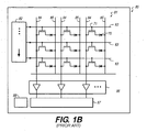
- FIG. 1A shows a cross-section (not to scale) of a single imaging pixel 10 in a prior art a-Si-based flat panel imager used in the indirect method and FIG. 1B shows a schematic top-view of a plat panel imager 80 including an array of such pixels 10.
- Each imaging pixel 10 has a photodiode 70 and a TFT switch 71.
- a layer of X-ray converter e.g., luminescent phosphor screen 12
- Photodiode 70 comprises the following layers: a passivation layer 14, an indium tin oxide layer 16, a p-doped Si layer 18, an intrinsic a-Si:H layer 20, an n-doped Si layer 22, a metal layer 24, a dielectric layer 26, and a glass substrate 28.
- An X-ray photon path 30 and a visible light photon path 32 are also shown in FIG. 1A . As illustrated, when a single X-ray is absorbed by the phosphor, a large number of light photons are emitted isotropically. Only a fraction of the emitted light reaches the photodiode and gets detected.
- the flat panel imager 80 consists of a sensor array 81 including a matrix of the a-Si n-i-p photodiodes 70 and TFTs 71.
- Gate driver chips 82 are connected to the blocks of gate lines 83 and readout chips are connected to blocks of data lines 84 and bias lines 85.
- Each of the data lines 84 has an associated charge amplifier 86.
- the amplifiers preferably include double correlated sampling circuits with programmable filtering (not shown), and are in communication with an analog multiplexer 87, which in turn communicates with an analog-to-digital converter (ADC) 88, to stream out the digital image data at desired rates.
- ADC analog-to-digital converter
- a-Si based indirect flat panel imager The operation of the a-Si based indirect flat panel imager is known by those skilled in the art, and thus only a brief description is given here.
- Incident X-ray photons are converted to optical photons in the phosphor screen 12, and these optical photons are subsequently converted to electron-hole pairs within the a-Si:H n-i-p photodiodes 70.
- a reverse bias voltage is applied to the bias lines 85 to create an electric field (and hence a depletion region) across the photodiodes and enhance charge collection efficiency.
- the pixel charge capacity of the photodiodes is determined by the product of the bias voltage and the photodiode capacitance.
- the image signal is integrated by the photodiodes while the associated TFTs 71 are held in a non-conducting ("off") state. This is accomplished by maintaining the gate lines 83 at a negative voltage.
- the array is read out by sequentially switching rows of TFTs to a conducting state by means of TFT gate control circuitry. When a row of pixels is switched to a conducting ("on") state by applying a positive voltage to the corresponding gate line 83, charge from those pixels is transferred along the data lines 84 and integrated by the external charge-sensitive amplifiers 86. The row is then switched back to a non-conducting state, and the process is repeated for each row until the entire array has been read out.
- the signal outputs from the external charge-sensitive amplifiers 86 are transferred to the analog-to-digital converter (ADC) 88 by the parallel-to-serial multiplexer 87, subsequently yielding a digital image.
- ADC analog-to-digital converter
- the flat panel imager is capable of both single-shot (radiographic) and continuous (fluoroscopic) image acquisition.
- the conventional scintillating phosphor screen imaging panel has three basic components: a substrate of glass or other rigid, transparent material, a TFT layer formed on the substrate, and a phosphor layer containing the scintillator material.
- the present invention relates to a projection radiographic imaging apparatus that includes a scintillator and an imaging array.
- the imaging array includes a plurality of pixels formed directly on a side of the scintillator.
- Each of the pixels includes at least one photosensor and at least one readout element.
- the present invention includes a method of making a radiographic imaging device. That method includes a step of forming a release layer on a temporary substrate. The method also includes forming an imaging array including a plurality of photosensors and a plurality of thin-film transistor readout elements on the release layer. A scintillator is formed on the imaging array, and the release layer is activated to remove the array from the temporary substrate.
- the present invention provides a radiographic imaging panel that includes a first scintillator having a first thickness and a second scintillator having a second thickness.
- An imaging array is formed on the first scintillator and disposed between the first and second scintillators.
- the imaging array includes a plurality of photosensors and a plurality of thin-film transistor readout element.
- the present invention provides a radiographic imaging panel including first and second scintillators, having respective first and second thicknesses, and an imaging array disposed directly on one of the first and second scintillators.
- the imaging array includes a plurality of pixel elements and is positioned between the first and second scintillators.
- Each pixel element includes a first photosensor optically coupled to the first scintillator, a second photosensor optically coupled to the second scintillator, and a readout element electrically coupled to the first and second photosensors and disposed directly on one of the first and second scintillators.
- an X-ray imaging plate may be exposed in any orientation, where stacked layers extend in generally horizontal, vertical, or oblique directions.
- the scintillator material of the imaging panel serves as the substrate on which photosensor and TFT readout elements are formed. That is, a separate substrate layer is not needed; the scintillator material serves as the substrate for an imaging panel.
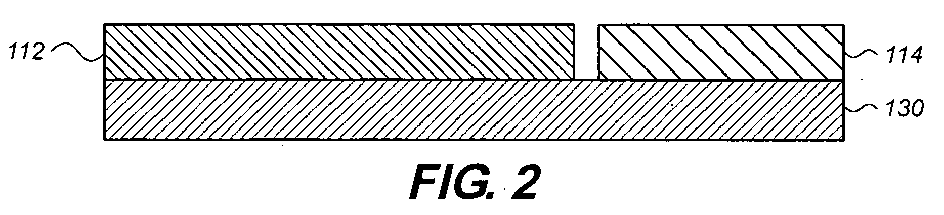
- the pixel element 110 includes a photosensor 112 and a readout element 114. (illustrated in FIG. 2 as, but not limited to, a TFT). Each pixel element 110 also includes a corresponding portion of a scintillator layer 130, or scintillating phosphor layer, that provides light energy to the photosensor 112.
- the scintillator layer 130 serves a dual-purpose function, namely, providing both the scintillating phosphor material and the substrate on which both photosensor 112 and TFT readout element 114 are disposed.
- Photosensor 112 can be any of a number of types of devices.
- photosensor 112 can be a segmented or non-segmented metal-insulating semiconductor (MIS).
- MIS metal-insulating semiconductor
- photosensor 112 can be a segmented or non-segmented photodiode or a phototransistor.
- Photosensors are generally well-known in the art, and the invention is not limited to any specific type of photosensor.
- FIG. 3 illustrates the structure of an alternate pixel element 210 for use in a projection radiographic imaging apparatus.
- This element is similar to that shown in FIG. 2 , but a scintillator layer 230 has a barrier layer 232, such as a thin coating, that isolates the scintillator layer 230 from a photosensor 212 and a TFT readout element 214.
- This arrangement allows the photosensor 212 and TFT readout element 214 to be formed on the scintillator layer 230, but with reduced likelihood that phosphor materials might diffuse into and degrade TFT semiconductor components.
- the barrier layer 232 can be an inorganic material such as silicon nitride, for example, or an organic material such as polyimide or BCB.
- the barrier layer 232 could alternately be a sol-gel.
- an alternate pixel element 310 has two, first and second, scintillator layers 330, 331, each with a corresponding thickness t1, t2.
- a photosensor 312 and a TFT readout element 314 are arranged between the first and second scintillator layers 330, 331, being formed on one of the scintillator layers 330, 331.
- FIG. 5 shows another embodiment of a pixel element 410, which combines the embodiments illustrated in FIGs. 3 and 4 .
- a barrier layer 432 lies between the imaging electronics of a photosensor 412 and a TFT readout element 414 and a second scintillator layer 431.
- a first scintillator layer 430 is formed on a side of the photosensor 412 and readout element 414 opposite the second scintillator layer 431.
- the barrier layer could instead be between the photosensor 412 and the TFT readout element 414 and first scintillator 430.
- two barrier layers could be provided, one between the photosensor 412 and the TFT 414 and each of the scintillators 430, 431.
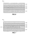
- FIG. 6 illustrates yet another embodiment of a pixel element 510 according to the invention.
- first and second photosensors 512, 513 are stacked atop each other.
- An opaque light shield layer 522 is provided between the first and second photosensors 512, 513.
- the light shield layer 522 helps to isolate the first photosensor 512 so that it receives light only from the first scintillator layer 530.
- the light shield layer 522 helps to isolate the second photosensor 513 so that it receives light only from the second scintillator layer 531.
- the pixel element 510 shown in FIG. 6 preferably also includes one or more readout elements associated with the photosensors 512, 513.
- FIG. 7 shows just such an embodiment.
- a pixel element 610 includes first and second photosensors 612, 613 separated by a light shield layer 622.
- the first photosensor 612 is formed on a first scintllator layer 630 and the second photosensor 613 is formed on a second scintillator layer 631.
- a readout element 614 also is included in this.embodiment.
- the second photosensor 613 and the TFT readout element 614 are formed on the same layer, that is, fabricated on the same plane.
- the TFT readout element 614 preferably is used to read photosensor values from each layer with this arrangement.
- the readout elements 614 alternatively could be present on the same layer as first photosensor 612 or could be on an entirely different layer.
- FIG. 8 shows another novel pixel element 710 in which first and second photosensors 712, 713 are stacked, with a switching TFT readout element 714 arranged to a side of the stack.
- Multiple light shield layers 722 are used in this embodiment, to help prevent optical crosstalk as well as to limit the exposure of the TFT readout element 714 to illumination, which can add noise to the x-ray data.
- the TFT readout, element 714 is formed on the second scintillator layer 731, fabricated on the same plane as the second photosensor 713. This places the thin-film transistor readout element 714 alongside the stacked photosensors 712, 713, which are respectively formed on the first and second scintillator layers 730, 731.
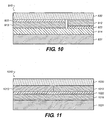
- FIG. 9 shows an alternate pixel element 810 in which two photosensors 812, 813 and a switching TFT readout element 814 are formed in the same plane. Protection in the form of light shield layer 822 is provided on both sides of the switching TFT readout element 814. Scintillator layers are noted as 830 and 831.
- a pixel element 910 includes first and second photosensors 912, 913 fabricated side by side, in the same plane on a first scintillator layer 930, with TFT readout elements 914 disposed on a second scintillator layer 931. Protection in the form of light shield layer 922 is provided on both sides of the switching TFT readout elements 914.
- the pixel element 1010 includes first and second photosensors 1012, 1013 arranged side-by-side and stacked atop a third photosensor 1016.
- pixel element 1010 includes multiple photosensing elements, each exhibiting a different response, depending on the spectral content of the emitted light. Protection in the form of light shield layer 1022 is provided. Scintillator layers are noted as 1030 and 1031. TFT readout elements are not shown in this view, although such could be included in arrangements illustrated in FIGs. 12 and 13 .
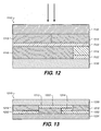
- FIG. 12 shows a pixel element 1110 in which first, second, and third photosensors 1112, 1113, and 1116 are included and a TFT readout element 1114 is formed alongside the third photosensor 1116. Also illustrated in FIG. 12 is the direction of X-ray radiation for this design, in one embodiment.
- the radiation is first absorbed close to the surface of a second scintillator layer 1131, opposite a first scintillator layer 1130, illumination excited from this layer suffers less optical scattering and the resulting image has higher MTF as a result.
- a light shield layer 1122 also may be provided, such as is illustrated.
- a pixel 1210 again has three photosensors 1212, 1213, 1216, wherein the different photosensors 1212, 1213, 1216 exhibit different responses, depending on the spectral content of the emitted light.
- a TFT readout element 1214 is disposed in the same plane or layer as all three photosensors 1212, 1213, 1216.
- Multiple light shield layers 1222 also may be provided, such as is illustrated to shield light emitted from first and second scintillators 1230, 1231.
- an imaging array including at least one of a photosensor and a readout element is formed directly on a scintillator.
- a substrate as is conventionally used and upon which the imaging array conventionally is formed.
- These embodiments may also be used in connection with conventional designs using a substrate. For example, when two scintillator layers are used, components of the imaging array may be formed directly on one of the scintillators, as described herein, and other components of the imaging array may be formed on a substrate, on which the other of the scintillator layers also is disposed.
- the two scintillators with accompanying imaging array components may then be "laminated" after construction.
- the benefits of reducing scatter resulting from the substrate are still obtained with one scintillator, whereas the substrate could still provide some structural stability.
- Several preferred embodiments of the invention include two scintillator layers of preferably differing thicknesses (although the scintillator layers could be the same thickness).
- the approach of these embodiments is to utilize multiple scintillator layers in a DR imaging plate to maximize the somewhat conflicting requirements for signal to noise ratio (SNR) and modulation transfer function (MTF).
- the first scintillator layer has thickness t1 that is relatively thinner than thickness t2 of the second scintillator layer.
- the thinner scintillator layer is optimized for resolution and MTF.
- the thicker scintillator layer is optimized for SNR.
- the thickness of one phosphor screen may be 97 ⁇ m (having a coating weight of 45.3 mg/cm 2 of Gd202S:Tb), while the thickness of the other phosphor screen may be 186 ⁇ m (having a coating weight of 82.7 mg/cm 2 of Gd 2 O 2 S:Tb).
- the thinner phosphor screen may have a light control layer of black, absorptive material and the thicker phosphor screen may have a light control coating of black absorptive material.
- the spatial frequency at which the MTF would equal 50% (f 1/2 ) is 3.8 c/mm and 2.4 c/mm for the thinner phosphor screen and the thicker phosphor screen, respectively.
- the X-ray absorption efficiency of the thicker phosphor screen is 47% as compared to 29% for the thinner phosphor screen.
- the MTF of the thinner phosphor screen would exceed the MTF of the thicker phosphor screen such that the spatial frequency at which the MTF is 50% (f 1/2 for the first phosphor screen is higher than that for the second phosphor screen by at least 0.5 c/mm.
- the X-ray absorption efficiency of the second phosphor screen would exceed that of the first phosphor screen by at least 10%.
- the imaging array is capable of reading the resulting image from each of phosphor screens, so that the combined image can provide higher quality than is available with conventional DR systems with a single phosphor screen.
- the material composition of the phosphor screens useful in the embodiments of the invention can include one or more of Gd 2 O 2 S:Tb, Gd 2 O 2 S:Eu, Gd 2 O 3 :Eu, La 2 O 2 S:Tb, La 2 O 2 S, Y 2 O 2 S:Tb, CsI:T1, CsI:Na, CsBr:Tl, NaI:Tl, CaWO 4 , CaWO 4 :Tb, BaFBr:Eu, BaFCI:Eu, BaSO 4 :Eu, BaSrSO 4 , BaPbSO 4 , BaAl 12 O 19 :Mn, BaMgAl 10 O 17 :Eu, Zn 2 SiO 4 :Mn, (Zn,Cd)S:Ag, LaOBr, LaOBr:Tm, Lu 2 O 2 S:Eu, Lu 2 O 2 S:Tb, LuTaO 4 , HfO 2 :Ti, HfGeO 4 :
- the phosphor screens can be of the same or of different material composition.
- the phosphor screens may have the same phosphor material but with different particle size distributions, particle-to-binder ratios, packaging densities, or absorbing dye.
- the median particle size of phosphor material on the second phosphor screen may be in the range from about 1 to about 5 microns, whereas the median particle size of phosphor material on the first phosphor screen may be in the range from about 6 to about 15 microns.
- the atomic number of heavy elements may differ in phosphor screens useful in the embodiments of the invention.
- the second phosphor screen may have a composition having an element of higher atomic number than that of the first phosphor screen.
- the second phosphor screen may contain Gd 2 O 2 S:Tb while the first phosphor screen may contain Y 2 O 2 S:Tb.
- Gadolinium (Gd) has an atomic number of 64
- yttrium (Y) has an atomic number of 39.
- the spatial frequency response of phosphor screens useful in the embodiments of the invention may be different-with the use of different phosphor materials with different structures.
- the second phosphor screen may comprise a columnar structured phosphor such as CsI:Tl
- the first phosphor screen may comprise a powder phosphor such as Gd 2 O 2 S:Tb.
- a layer of CsI will condense in the form of needle-like, closely packed crystallites with high packing density.
- Such a columnar or needle-like phosphor is well known in the art.
- the second phosphor screen may have a CsI:Tl layer with a thickness of 89 microns, while the first phosphor screen may have a Gd 2 O 2 S:Tb layer with a thickness of 93 microns.
- the spatial frequency response of the second phosphor screen may be higher than that of the first phosphor screen.
- the values of the spatial frequency at which the MTF equals 50% (f 1/2 ) are 4.7 c/mm and 3.3 c/mm for the second and first phosphor screens, respectively.
- x-ray radiation generally is incident on the side of the imaging device having the thinner phosphor screen, i.e., the thinner screen is arranged closer to the x-ray source. In this manner, MTF of the thinner screen is optimized.
- x-ray radiation may be incident on the thicker of phosphor screens, such that the SNR of the thicker screen is optimized.
- thicknesses t1, t2 of the scintillator layers may be scaled in order to optimize optical absorption lengths. For example, thicknesses exceeding one or more absorption length can be beneficial for reducing optical crosstalk.
- the light shield may be metal or some other opaque material and may also provide an electrical connection, such as a contact, for example.
- the light shield additionally/alternatively may be a colorant and/or a semiconductor.
- the photosensors may be identical, exhibiting the same overall response to incident radiation of different wavelengths.
- the photosensors may have different sensitivity characteristics, "tuned" to match the emission characteristics of their corresponding scintillator layer.
- one scintillator layer may emit light with a peak value near 500 nm and the other scintillator layer, could have a different phosphor material, which may emit light with a peak value near 550 nm, for example.
- the photosensors and/or the readout elements are disposed directly on the scintillator layer according to the invention, without an intervening substrate.
- these imaging components are fabricated directly on the scintillator layer using known fabrication techniques. Preferred embodiments of this method include using Gd 2 O 2 S:Tb as the scintillator layer.
- this method include using Gd 2 O 2 S:Tb as the scintillator layer.
- the imaging components may be formed first on an intermediate or temporary substrate, then laminated onto the scintillator layer.
- One method using the intermediate substrate includes forming a release layer on the intermediate substrate. Then the array consisting of photosensors and thin-film transistor readout elements are formed on the release layer. Next, radiant energy, heat, pressure, or other energy is applied to the release layer in order to separate it from the intermediate substrate. The release layer or some other substance or process then may be used to adhere or otherwise bond the array of imaging pixels to the scintillator to form an imaging panel.
- the release layer used in accordance with the invention may be organic or inorganic and may be chemically-, optically-, or thermally-activated. Known release layers include ProLIFT, commercially available from Brewer Science and HD-3007 polyimide adhesive, a laser-activated release commercially available from HD Microsystems. The release layer also may include polybenzoxazole.
- a temporary substrate is provided. Like in the embodiment just described, a release layer is formed on a substantially planar surface of the temporary substrate and the imaging array, including photosensitive elements and switching elements, is formed on the release layer. While the array and release layer are still disposed on the temporary substrate; the scintillator is bonded on the imaging array. The release layer is thereafter activated, to separate the imaging array (with scintillator bonded thereto) from the temporary substrate. Accordingly, an imaging array as exemplified in Figure 2 is obtained.
- the release layer preferably is an organic or an inorganic material that can be thermally-, optically-, and/or chemically-activated.
- the release layer is activated using etching techniques.
- a barrier layer may be used between the release layer and the imaging array and the etch used has a high selectivity of etch rate to the barrier layer, to avoid damaging the imaging array.
- the etch could be, for example, a xenon difloride gas.
- the release layer may include a colorant. To activate the release layer, radiant energy is directed to the release layer and the colorant absorbs at least a portion of the radiant energy.
- the release layers described above also may be used in this embodiment.
- a barrier layer may be include to act as an etch stop
- a barrier layer may be formed between the imaging array and the scintillator, to form a device such as that illustrated in Figure 3 .
- a planarization layer may be formed on the imaging array prior to boding the scintillator, to provide a substantially planar surface upon which the scintillator is bonded.
- a second scintillator can be bonded on the surface of the imaging array exposed upon such removal.
- the second scintillator has properties different from the properties of the first scintillator. Adding the second scintillator in this manner will form devices such as those shown in Figures 4 and 5 .
- two arrays with bonded substrates may be laminated after construction using an adhesive or the like, to produce the array exemplified in Figures 6 and 7 .
- the remaining illustrated arrays can be formed in like manner by appropriately forming the imaging arrays on the release layer. Barrier layers also can be formed using known methods to yield the desired pixel structure.
- photodiodes were used as the exemplary light sensing elements in the foregoing embodiments, the invention is not limited in this regard.
- Any photosensitive element could be used, including, but not limited to, metal-insulating-semiconductors, p-n junction photodiodes, PIN photodiodes, pinned photodiodes, charge-injection-devices, charge-coupled devices, and phototransistors.
- the invention also is not limited TFTs as the readout elements. Any of MOS transistors, bipolar transistors, diode switches, charge-injection-devices, and charge-coupled devices could be used.
- the imaging array may be formed in any of amorphous silicon, polycrystalline silicon, single-crystal silicon, organic semiconductors, and one or more of binary, ternary, or quaternary semiconductors containing one of indium, zinc, oxygen, and gallium, or any combination thereof.
Landscapes
- Physics & Mathematics (AREA)
- Health & Medical Sciences (AREA)
- Life Sciences & Earth Sciences (AREA)
- General Physics & Mathematics (AREA)
- High Energy & Nuclear Physics (AREA)
- Molecular Biology (AREA)
- Spectroscopy & Molecular Physics (AREA)
- Chemical & Material Sciences (AREA)
- Crystallography & Structural Chemistry (AREA)
- Measurement Of Radiation (AREA)
- Solid State Image Pick-Up Elements (AREA)
- Apparatus For Radiation Diagnosis (AREA)
Abstract
Description
- This invention generally relates to digital radiographic imaging and more particularly relates to a flat panel imaging apparatus having a scintillating phosphor screen with an imaging array of photosensors and thin-film transistor readout devices formed directly on the scintillating phosphor screen.
- Generally, medical X-ray detectors employing a scintillating phosphor screen to absorb X-rays and produce light suffer the loss of spatial resolution due to lateral light diffusion in the phosphor screen. To reduce lateral light diffusion and maintain acceptable spatial resolution, the phosphor screens must be made sufficiently thin.
- The spatial resolution and X-ray detection ability of an imaging apparatus are often characterized by the modulation transfer function (MTF) and X-ray absorption efficiency, respectively. Thin phosphor screens produce better MTF at the expense of reduced X-ray absorption. Usually, the coating density and the thickness of the phosphor screen are used in the design tradeoff between spatial resolution and X-ray absorption efficiency.
- For example, the Lanex Fine and the Lanex Fast Back screens are two typical commercial screens, both manufactured by Eastman Kodak Co. Both are made of Gd2O2S(Tb) phosphor. The Lanex Fast Back screen is relatively thicker and absorbs X-rays more efficiently, but has lower resolution than the Lanex Fine screen. On the other hand, the Lanex Fine screen is thinner than the Lanex Fast Back screen, absorbs X-rays relatively less efficiently, but has higher resolution. The coating density of the Lanex Fine and the Lanex Fast Back screens are 34 mg/cm2 and 133 mg/cm2, respectively. The Lanex Fine and the Lanex Fast Back screens have X-ray absorption efficiencies of 24% and 63% (for 80 kVp, with tungsten target, 2.5-mm Al inherent filtration, and filtered by 0.5-mm Cu + 1.0-mm Al) and MTF values of 0.26 and 0.04 at 5 c/mm, respectively.
- Recently, digital flat panel X-ray imagers based upon active matrix thin film electronics have become a promising technology for applications such as diagnostic radiology and digital mammography. There are two types of X-ray energy conversion methods used in digital radiography (DR), namely, the direct and indirect method. In the direct method, the X-rays absorbed in a photoconductor are directly transduced into a charge signal, stored on the pixel electrodes on an active matrix array (AMA) and read out using thin film transistors (TFTs) to produce a digital image. Amorphous selenium (a-Se) is usually used as the photoconductor.
- In the indirect method, a single phosphor screen is used to absorb X-rays and the resultant light photons are detected by an AMA with a single photodiode (PD) and a TFT switch at each pixel. The photodiode absorbs the light given off by the phosphor in proportion to the X-ray energy absorbed. The stored charge is then read out, like the direct method, using the TFT switch. Common phosphor materials include powder phosphors such as Gd2O2S(Tb) and structured phosphors such as CsI(T1). Amorphous hydrogenated silicon (a-Si:H) is commonly used to form the photodiode and the TFT switch in the indirect method.
-
FIG. 1A shows a cross-section (not to scale) of a single imaging pixel 10 in a prior art a-Si-based flat panel imager used in the indirect method andFIG. 1B shows a schematic top-view of aplat panel imager 80 including an array of such pixels 10. Each imaging pixel 10 has aphotodiode 70 and aTFT switch 71. A layer of X-ray converter (e.g., luminescent phosphor screen 12) is coupled to the photodiode-TFT array.Photodiode 70 comprises the following layers: a passivation layer 14, an indiumtin oxide layer 16, a p-dopedSi layer 18, an intrinsic a-Si:H layer 20, an n-dopedSi layer 22, ametal layer 24, adielectric layer 26, and aglass substrate 28. AnX-ray photon path 30 and a visiblelight photon path 32 are also shown inFIG. 1A . As illustrated, when a single X-ray is absorbed by the phosphor, a large number of light photons are emitted isotropically. Only a fraction of the emitted light reaches the photodiode and gets detected. - As shown in
FIG. 1B , theflat panel imager 80 consists of a sensor array 81 including a matrix of the a-Sin-i-p photodiodes 70 andTFTs 71.Gate driver chips 82 are connected to the blocks ofgate lines 83 and readout chips are connected to blocks ofdata lines 84 andbias lines 85. Each of thedata lines 84 has an associatedcharge amplifier 86. The amplifiers preferably include double correlated sampling circuits with programmable filtering (not shown), and are in communication with ananalog multiplexer 87, which in turn communicates with an analog-to-digital converter (ADC) 88, to stream out the digital image data at desired rates. - The operation of the a-Si based indirect flat panel imager is known by those skilled in the art, and thus only a brief description is given here. Incident X-ray photons are converted to optical photons in the
phosphor screen 12, and these optical photons are subsequently converted to electron-hole pairs within the a-Si:H n-i-p photodiodes 70. In general, a reverse bias voltage is applied to thebias lines 85 to create an electric field (and hence a depletion region) across the photodiodes and enhance charge collection efficiency. The pixel charge capacity of the photodiodes is determined by the product of the bias voltage and the photodiode capacitance. The image signal is integrated by the photodiodes while theassociated TFTs 71 are held in a non-conducting ("off") state. This is accomplished by maintaining thegate lines 83 at a negative voltage. The array is read out by sequentially switching rows of TFTs to a conducting state by means of TFT gate control circuitry. When a row of pixels is switched to a conducting ("on") state by applying a positive voltage to thecorresponding gate line 83, charge from those pixels is transferred along thedata lines 84 and integrated by the external charge-sensitive amplifiers 86. The row is then switched back to a non-conducting state, and the process is repeated for each row until the entire array has been read out. The signal outputs from the external charge-sensitive amplifiers 86 are transferred to the analog-to-digital converter (ADC) 88 by the parallel-to-serial multiplexer 87, subsequently yielding a digital image. The flat panel imager is capable of both single-shot (radiographic) and continuous (fluoroscopic) image acquisition. - The conventional scintillating phosphor screen imaging panel has three basic components: a substrate of glass or other rigid, transparent material, a TFT layer formed on the substrate, and a phosphor layer containing the scintillator material. There would be advantages in simplifying the design of the imaging panel and reducing size, weight, and cost by eliminating components that are not directly involved in obtaining the image data.
- It is an object of the present invention to provide a projection radiographic imaging apparatus that has a simplified and lightweight design and improved detection and display characteristics.
- In one aspect, the present invention relates to a projection radiographic imaging apparatus that includes a scintillator and an imaging array. The imaging array includes a plurality of pixels formed directly on a side of the scintillator. Each of the pixels includes at least one photosensor and at least one readout element.
- According to another aspect, the present invention includes a method of making a radiographic imaging device. That method includes a step of forming a release layer on a temporary substrate. The method also includes forming an imaging array including a plurality of photosensors and a plurality of thin-film transistor readout elements on the release layer. A scintillator is formed on the imaging array, and the release layer is activated to remove the array from the temporary substrate.
- In yet another embodiment, the present invention provides a radiographic imaging panel that includes a first scintillator having a first thickness and a second scintillator having a second thickness. An imaging array is formed on the first scintillator and disposed between the first and second scintillators. The imaging array includes a plurality of photosensors and a plurality of thin-film transistor readout element.
- According to a still further aspect, the present invention provides a radiographic imaging panel including first and second scintillators, having respective first and second thicknesses, and an imaging array disposed directly on one of the first and second scintillators. The imaging array includes a plurality of pixel elements and is positioned between the first and second scintillators. Each pixel element includes a first photosensor optically coupled to the first scintillator, a second photosensor optically coupled to the second scintillator, and a readout element electrically coupled to the first and second photosensors and disposed directly on one of the first and second scintillators.
- These and other objects, features, and advantages of the present invention will become apparent to those skilled in the art upon a reading of the following detailed description when taken in conjunction with the drawings wherein there is shown and described an illustrative embodiment of the invention.
- While the specification concludes with claims particularly pointing out and distinctly claiming the subject matter of the present invention, it is believed that the invention will be better understood from the following description when taken in conjunction with the accompanying drawings.
-
FIG. 1A is a cross-sectional view showing an imaging pixel in a prior art flat-panel imager. -
FIG. 1B is a schematic diagram showing components of a prior art flat-panel imager. -
FIG. 2 is a cross-sectional view of a pixel element according to one embodiment of the present invention. -
FIG. 3 is a cross-sectional view of a pixel element according to another embodiment of the invention. -
FIG. 4 is a cross-sectional view of a pixel element according to yet another preferred embodiment of the invention. -
FIG. 5 is a cross-sectional view of a pixel element according to yet another preferred embodiment of the invention. -
FIG. 6 is a cross-sectional view of a portion of a pixel element according to yet another preferred embodiment of the invention. -
FIG. 7 is a cross-sectional view of a pixel element according to still another preferred embodiment of the invention. -
FIG. 8 is a cross-sectional view of a pixel element according to still another preferred embodiment of the invention. -
FIG. 9 is a cross-sectional view of a pixel element according to yet another preferred embodiment of the invention. -
FIG. 10 is a cross-sectional view of a pixel element with dual scintillator layers and multiple photosensors, with light shields and TFT readout circuitry connecting to each photosensor and on a separate layer. -
FIG. 11 is a cross-sectional view of a pixel element according to yet another preferred embodiment of the invention. -
FIG. 12 is a cross-sectional view of a pixel element according to yet another preferred embodiment of the invention. -
FIG. 13 is a cross-sectional view of a pixel element according to yet another preferred embodiment of the invention. - The present description is directed in particular to elements forming part of, or cooperating more directly with, apparatuses and methods in accordance with the invention. It is to be understood that elements not specifically shown or described may take various forms well known to those skilled in the art.
- In the description that follows, terms and phrases such as "above" or "on top of" are used in a broad sense, to indicate an arrangement of layers relative to each other. Certainly, an X-ray imaging plate may be exposed in any orientation, where stacked layers extend in generally horizontal, vertical, or oblique directions.
- The general approach of the present invention eliminates the need for a separate substrate material in forming an imaging panel for radiographic imaging. In the various embodiments of the present invention, the scintillator material of the imaging panel serves as the substrate on which photosensor and TFT readout elements are formed. That is, a separate substrate layer is not needed; the scintillator material serves as the substrate for an imaging panel.
- Referring to
FIG. 2 , there is shown, in cross-section, the structure of a pixel element 110 for use on an imaging panel of a projection radiographic imaging apparatus according to a preferred embodiment of the invention. The pixel element 110 includes aphotosensor 112 and areadout element 114. (illustrated inFIG. 2 as, but not limited to, a TFT). Each pixel element 110 also includes a corresponding portion of ascintillator layer 130, or scintillating phosphor layer, that provides light energy to thephotosensor 112. Thescintillator layer 130 serves a dual-purpose function, namely, providing both the scintillating phosphor material and the substrate on which both photosensor 112 andTFT readout element 114 are disposed. -
Photosensor 112 can be any of a number of types of devices. For example,photosensor 112 can be a segmented or non-segmented metal-insulating semiconductor (MIS). Alternately,photosensor 112 can be a segmented or non-segmented photodiode or a phototransistor. Photosensors are generally well-known in the art, and the invention is not limited to any specific type of photosensor. -
FIG. 3 illustrates the structure of an alternate pixel element 210 for use in a projection radiographic imaging apparatus. This element is similar to that shown inFIG. 2 , but a scintillator layer 230 has a barrier layer 232, such as a thin coating, that isolates the scintillator layer 230 from aphotosensor 212 and aTFT readout element 214. This arrangement allows thephotosensor 212 andTFT readout element 214 to be formed on the scintillator layer 230, but with reduced likelihood that phosphor materials might diffuse into and degrade TFT semiconductor components. The barrier layer 232 can be an inorganic material such as silicon nitride, for example, or an organic material such as polyimide or BCB. The barrier layer 232 could alternately be a sol-gel. - Referring to
FIG. 4 , there is shown another embodiment of the invention in which an alternate pixel element 310 has two, first and second, scintillator layers 330, 331, each with a corresponding thickness t1, t2. In this embodiment, aphotosensor 312 and aTFT readout element 314 are arranged between the first and second scintillator layers 330, 331, being formed on one of the scintillator layers 330, 331. -
FIG. 5 shows another embodiment of apixel element 410, which combines the embodiments illustrated inFIGs. 3 and4 . Here, abarrier layer 432 lies between the imaging electronics of aphotosensor 412 and aTFT readout element 414 and asecond scintillator layer 431. Afirst scintillator layer 430 is formed on a side of thephotosensor 412 andreadout element 414 opposite thesecond scintillator layer 431. In an alternative embodiment, the barrier layer could instead be between the photosensor 412 and theTFT readout element 414 andfirst scintillator 430. Moreover, two barrier layers could be provided, one between the photosensor 412 and theTFT 414 and each of thescintillators -
FIG. 6 illustrates yet another embodiment of apixel element 510 according to the invention. In this embodiment, first andsecond photosensors light shield layer 522 is provided between the first andsecond photosensors second photosensors light shield layer 522 helps to isolate thefirst photosensor 512 so that it receives light only from thefirst scintillator layer 530. Similarly, thelight shield layer 522 helps to isolate thesecond photosensor 513 so that it receives light only from thesecond scintillator layer 531. - Although not illustrated, the
pixel element 510 shown inFIG. 6 preferably also includes one or more readout elements associated with thephotosensors FIG. 7 shows just such an embodiment. InFIG. 7 , apixel element 610 includes first andsecond photosensors light shield layer 622. Thefirst photosensor 612 is formed on afirst scintllator layer 630 and thesecond photosensor 613 is formed on asecond scintillator layer 631. Areadout element 614 also is included in this.embodiment. As illustrated, thesecond photosensor 613 and theTFT readout element 614 are formed on the same layer, that is, fabricated on the same plane. TheTFT readout element 614 preferably is used to read photosensor values from each layer with this arrangement. Thereadout elements 614 alternatively could be present on the same layer asfirst photosensor 612 or could be on an entirely different layer. - Other arrangements also are contemplated. For example,
FIG. 8 shows another novel pixel element 710 in which first andsecond photosensors 712, 713 are stacked, with a switchingTFT readout element 714 arranged to a side of the stack. Multiple light shield layers 722 are used in this embodiment, to help prevent optical crosstalk as well as to limit the exposure of theTFT readout element 714 to illumination, which can add noise to the x-ray data. The TFT readout,element 714 is formed on the second scintillator layer 731, fabricated on the same plane as the second photosensor 713. This places the thin-filmtransistor readout element 714 alongside thestacked photosensors 712, 713, which are respectively formed on the first and second scintillator layers 730, 731. -
FIG. 9 shows analternate pixel element 810 in which twophotosensors TFT readout element 814 are formed in the same plane. Protection in the form oflight shield layer 822 is provided on both sides of the switchingTFT readout element 814. Scintillator layers are noted as 830 and 831. In a similar embodiment shown inFIG. 10 , apixel element 910 includes first andsecond photosensors first scintillator layer 930, withTFT readout elements 914 disposed on asecond scintillator layer 931. Protection in the form oflight shield layer 922 is provided on both sides of the switchingTFT readout elements 914. - Referring to
FIG. 11 , there is shown anotherpixel element 1010 according to the invention. In this embodiment, thepixel element 1010 includes first andsecond photosensors third photosensor 1016. Here,pixel element 1010 includes multiple photosensing elements, each exhibiting a different response, depending on the spectral content of the emitted light. Protection in the form oflight shield layer 1022 is provided. Scintillator layers are noted as 1030 and 1031. TFT readout elements are not shown in this view, although such could be included in arrangements illustrated inFIGs. 12 and 13 . - Specifically,
FIG. 12 shows apixel element 1110 in which first, second, andthird photosensors TFT readout element 1114 is formed alongside thethird photosensor 1116. Also illustrated inFIG. 12 is the direction of X-ray radiation for this design, in one embodiment. Here, since the radiation is first absorbed close to the surface of asecond scintillator layer 1131, opposite afirst scintillator layer 1130, illumination excited from this layer suffers less optical scattering and the resulting image has higher MTF as a result. Havingmultiple photosensors light shield layer 1122 also may be provided, such as is illustrated. - In
FIG. 13 , apixel 1210 again has threephotosensors different photosensors TFT readout element 1214 is disposed in the same plane or layer as all threephotosensors light shield layers 1222 also may be provided, such as is illustrated to shield light emitted from first andsecond scintillators - Thus, embodiments of imaging pixel elements according to the invention have been described. In each of these embodiments, an imaging array, including at least one of a photosensor and a readout element is formed directly on a scintillator. According to these embodiments, there is no need for a substrate, as is conventionally used and upon which the imaging array conventionally is formed. These embodiments may also be used in connection with conventional designs using a substrate. For example, when two scintillator layers are used, components of the imaging array may be formed directly on one of the scintillators, as described herein, and other components of the imaging array may be formed on a substrate, on which the other of the scintillator layers also is disposed. In such an embodiment, the two scintillators with accompanying imaging array components may then be "laminated" after construction. In this manner, the benefits of reducing scatter resulting from the substrate are still obtained with one scintillator, whereas the substrate could still provide some structural stability.
- Several preferred embodiments of the invention include two scintillator layers of preferably differing thicknesses (although the scintillator layers could be the same thickness). The approach of these embodiments is to utilize multiple scintillator layers in a DR imaging plate to maximize the somewhat conflicting requirements for signal to noise ratio (SNR) and modulation transfer function (MTF). In the embodiments, the first scintillator layer has thickness t1 that is relatively thinner than thickness t2 of the second scintillator layer. With inherently less optical light diffusion, the thinner scintillator layer is optimized for resolution and MTF. Conversely, the thicker scintillator layer is optimized for SNR. For example, the thickness of one phosphor screen may be 97 µm (having a coating weight of 45.3 mg/cm2 of Gd202S:Tb), while the thickness of the other phosphor screen may be 186 µm (having a coating weight of 82.7 mg/cm2 of Gd2O2S:Tb). The thinner phosphor screen may have a light control layer of black, absorptive material and the thicker phosphor screen may have a light control coating of black absorptive material. Using the typical X-ray beam for general radiography (the DN5 RQA5 beam), the spatial frequency at which the MTF would equal 50% (f1/2) is 3.8 c/mm and 2.4 c/mm for the thinner phosphor screen and the thicker phosphor screen, respectively. At the same time, the X-ray absorption efficiency of the thicker phosphor screen is 47% as compared to 29% for the thinner phosphor screen. In practical designs, the MTF of the thinner phosphor screen would exceed the MTF of the thicker phosphor screen such that the spatial frequency at which the MTF is 50% (f1/2 for the first phosphor screen is higher than that for the second phosphor screen by at least 0.5 c/mm. In addition, the X-ray absorption efficiency of the second phosphor screen would exceed that of the first phosphor screen by at least 10%. The imaging array is capable of reading the resulting image from each of phosphor screens, so that the combined image can provide higher quality than is available with conventional DR systems with a single phosphor screen.
- The material composition of the phosphor screens useful in the embodiments of the invention can include one or more of Gd2O2S:Tb, Gd2O2S:Eu, Gd2O3:Eu, La2O2S:Tb, La2O2S, Y2O2S:Tb, CsI:T1, CsI:Na, CsBr:Tl, NaI:Tl, CaWO4, CaWO4:Tb, BaFBr:Eu, BaFCI:Eu, BaSO4:Eu, BaSrSO4, BaPbSO4, BaAl12O19:Mn, BaMgAl10O17:Eu, Zn2SiO4:Mn, (Zn,Cd)S:Ag, LaOBr, LaOBr:Tm, Lu2O2S:Eu, Lu2O2S:Tb, LuTaO4, HfO2:Ti, HfGeO4:Ti, YTaO4, YTaO4:Gd , YTaO4:Nb, Y2O3:Eu, YBO3:Eu, YBO3:Tb, or (Y,Gd)BO3:Eu, or combinations thereof. The phosphor screens, for instance, can be of the same or of different material composition. For example, the phosphor screens may have the same phosphor material but with different particle size distributions, particle-to-binder ratios, packaging densities, or absorbing dye. The median particle size of phosphor material on the second phosphor screen may be in the range from about 1 to about 5 microns, whereas the median particle size of phosphor material on the first phosphor screen may be in the range from about 6 to about 15 microns.
- The atomic number of heavy elements may differ in phosphor screens useful in the embodiments of the invention. For example, for higher X-ray energy absorption, the second phosphor screen may have a composition having an element of higher atomic number than that of the first phosphor screen. In one instance, the second phosphor screen may contain Gd2O2S:Tb while the first phosphor screen may contain Y2O2S:Tb. Gadolinium (Gd) has an atomic number of 64, whereas yttrium (Y) has an atomic number of 39.
- Moreover, the spatial frequency response of phosphor screens useful in the embodiments of the invention may be different-with the use of different phosphor materials with different structures. For example, the second phosphor screen may comprise a columnar structured phosphor such as CsI:Tl, while the first phosphor screen may comprise a powder phosphor such as Gd2O2S:Tb. When evaporated under appropriate conditions, a layer of CsI will condense in the form of needle-like, closely packed crystallites with high packing density. Such a columnar or needle-like phosphor is well known in the art. See, for example, ALN Stevels et al., "Vapor Deposited CsI:Na Layers: Screens for Application in X-Ray Imaging Devices," Philips Research Reports 29:353-362 (1974); and T. Jing et al, "Enhanced Columnar Structure in CsI Layer by Substrate Patterning", IEEE Trans. Nucl. Sci. 39: 1195-1198 (1992): In this form, the spatial frequency response (or resolution) is improved over that for a powder phosphor screen of the same thickness, presumably because the columnar crystallites enhance the forward scattering of the light compared to a powder phosphor screen. These columns can be thought to act like fiber optic light guides such that light photons produced by the absorption of an incident X-ray will be guided toward either end of the pillars. Similar to powder screens, a reflective backing is used to maximize the light collection capabilities of the layer by redirecting light photons toward the exit surface. For example, the second phosphor screen may have a CsI:Tl layer with a thickness of 89 microns, while the first phosphor screen may have a Gd2O2S:Tb layer with a thickness of 93 microns. The spatial frequency response of the second phosphor screen may be higher than that of the first phosphor screen. The values of the spatial frequency at which the MTF equals 50% (f1/2) are 4.7 c/mm and 3.3 c/mm for the second and first phosphor screens, respectively.
- In these dual screen devices, x-ray radiation generally is incident on the side of the imaging device having the thinner phosphor screen, i.e., the thinner screen is arranged closer to the x-ray source. In this manner, MTF of the thinner screen is optimized. Alternatively, x-ray radiation may be incident on the thicker of phosphor screens, such that the SNR of the thicker screen is optimized.
- Also in the dual screen devices, thicknesses t1, t2 of the scintillator layers may be scaled in order to optimize optical absorption lengths. For example, thicknesses exceeding one or more absorption length can be beneficial for reducing optical crosstalk.
- Also in the embodiments described above, the light shield may be metal or some other opaque material and may also provide an electrical connection, such as a contact, for example. The light shield additionally/alternatively may be a colorant and/or a semiconductor.
- When more than one photosensor is present in the foregoing embodiments, they may be identical, exhibiting the same overall response to incident radiation of different wavelengths. However, in other embodiments, the photosensors may have different sensitivity characteristics, "tuned" to match the emission characteristics of their corresponding scintillator layer. For example, one scintillator layer may emit light with a peak value near 500 nm and the other scintillator layer, could have a different phosphor material, which may emit light with a peak value near 550 nm, for example.
- As noted in the foregoing embodiments, the photosensors and/or the readout elements are disposed directly on the scintillator layer according to the invention, without an intervening substrate. In one method of forming this apparatus, these imaging components are fabricated directly on the scintillator layer using known fabrication techniques. Preferred embodiments of this method include using Gd2O2S:Tb as the scintillator layer. Moreover, to ensure proper formation of the imaging components on the scintillator, generally it is desirable to maintain a planarity of the scintillator layer to within 20 nm RMS.
- In another preferred embodiment, the imaging components may be formed first on an intermediate or temporary substrate, then laminated onto the scintillator layer. One method using the intermediate substrate includes forming a release layer on the intermediate substrate. Then the array consisting of photosensors and thin-film transistor readout elements are formed on the release layer. Next, radiant energy, heat, pressure, or other energy is applied to the release layer in order to separate it from the intermediate substrate. The release layer or some other substance or process then may be used to adhere or otherwise bond the array of imaging pixels to the scintillator to form an imaging panel. The release layer used in accordance with the invention may be organic or inorganic and may be chemically-, optically-, or thermally-activated. Known release layers include ProLIFT, commercially available from Brewer Science and HD-3007 polyimide adhesive, a laser-activated release commercially available from HD Microsystems. The release layer also may include polybenzoxazole.
- In another method of fabricating arrays on a scintillator, a temporary substrate is provided. Like in the embodiment just described, a release layer is formed on a substantially planar surface of the temporary substrate and the imaging array, including photosensitive elements and switching elements, is formed on the release layer. While the array and release layer are still disposed on the temporary substrate; the scintillator is bonded on the imaging array. The release layer is thereafter activated, to separate the imaging array (with scintillator bonded thereto) from the temporary substrate. Accordingly, an imaging array as exemplified in
Figure 2 is obtained. - The release layer preferably is an organic or an inorganic material that can be thermally-, optically-, and/or chemically-activated. For example, in one embodiment the release layer is activated using etching techniques. In such an embodiment, a barrier layer may be used between the release layer and the imaging array and the etch used has a high selectivity of etch rate to the barrier layer, to avoid damaging the imaging array. The etch could be, for example, a xenon difloride gas. In yet another embodiment, the release layer may include a colorant. To activate the release layer, radiant energy is directed to the release layer and the colorant absorbs at least a portion of the radiant energy. The release layers described above also may be used in this embodiment.
- While the barrier layer may be include to act as an etch stop, a barrier layer may be formed between the imaging array and the scintillator, to form a device such as that illustrated in
Figure 3 . In still other embodiments, a planarization layer may be formed on the imaging array prior to boding the scintillator, to provide a substantially planar surface upon which the scintillator is bonded. - Variations of the foregoing methods also are contemplated and can be used to form the preferred imaging arrays of the present invention. For example, once the imaging array and scintillator are removed from the temporary substrate, a second scintillator can be bonded on the surface of the imaging array exposed upon such removal. Preferably, the second scintillator has properties different from the properties of the first scintillator. Adding the second scintillator in this manner will form devices such as those shown in
Figures 4 and 5 . Moreover, two arrays with bonded substrates may be laminated after construction using an adhesive or the like, to produce the array exemplified inFigures 6 and 7 . The remaining illustrated arrays can be formed in like manner by appropriately forming the imaging arrays on the release layer. Barrier layers also can be formed using known methods to yield the desired pixel structure. - The invention has been described in detail with particular reference to certain preferred embodiments thereof, but it will be understood that variations and modifications can be effected within the scope of the invention as described above, and as noted in the appended claims, by a person of ordinary skill in the art without departing from the scope of the invention.
- For example, although photodiodes were used as the exemplary light sensing elements in the foregoing embodiments, the invention is not limited in this regard. Any photosensitive element could be used, including, but not limited to, metal-insulating-semiconductors, p-n junction photodiodes, PIN photodiodes, pinned photodiodes, charge-injection-devices, charge-coupled devices, and phototransistors. The invention also is not limited TFTs as the readout elements. Any of MOS transistors, bipolar transistors, diode switches, charge-injection-devices, and charge-coupled devices could be used. Moreover, the imaging array may be formed in any of amorphous silicon, polycrystalline silicon, single-crystal silicon, organic semiconductors, and one or more of binary, ternary, or quaternary semiconductors containing one of indium, zinc, oxygen, and gallium, or any combination thereof.
- Thus, what is provided is an imaging array of photosensors and thin-film transistor readout devices formed directly on a scintillating phosphor screen.
-
- 10. Imaging pixel
- 12. Phosphor screen
- 14. Passivization layer
- 16. Indium-tin-oxide layer
- 18. p-doped Si layer
- 20. a-Si:H layer
- 22. n-doped Si layer
- 24. Metal layer
- 26. Dielectric layer
- 28. Glass substrate
- 30. X-ray photon path
- 32. Visible light photon path
- 70. Photodiode
- 71. TFT switch
- 80. Flat panel imager
- 81. Sensor array
- 82. Driver chip
- 83. Gate lines
- 84. Data line
- 85. Bias line
- 86. Amplifier
- 87. Multiplexer
- 88. A-D converter
- 110, 210, 310, 410, 510, 610, 710, 810, 910, 1010, 1110, 1210. Pixel element
- 112, 212, 312, 412, 512, 612, 712, 812, 912, 1012, 1112, 1212. (First) Photosensor
- 513, 613, 713, 813, 913, 1013, 1113, 1213. Second Photosensor
- 114, 214, 314, 414, 614, 714, 814, 914, 1114, 1214. TFT readout element
- 1016, 1116, 1216. Third Photosensor
- 522, 622, 722, 822, 922, 1022, 1122, 1222. Light shield layer
- 130, 230, 330, 430, 530, 630, 730, 830, 930, 1030, 1130, 1230. (First) Scintillator layer
- 331, 431, 531, 631, 731, 831, 931, 1031, 1131, 1231. Second Scintillator layer
- 232, 432. Barrier layer
- t1, t2. Thickness
Claims (15)
- A projection radiographic imaging apparatus, comprising:a scintillator; andan imaging array comprising a plurality of pixels formed directly on a side of the scintillator, each of the pixels comprising at least one photosensor and at least one readout element.
- The apparatus of claim 1 wherein the at least one photosensor includes one or more of a metal-insulating-semiconductor, a p-n junction photodiode, a PIN photodiode, a pinned photodiode, a charge-injection-device, a charge-coupled device, and a phototransistor.
- The apparatus of claim 1 wherein the at least, one readout element comprises one or more of a thin film transistor, a MOS transistor, a bipolar transistor, a diode switch, a charge-injection-device, and a charge-coupled device.
- The apparatus of claim 1, wherein the scintillator is a first scintillator and further comprising a second scintillator disposed to sandwich the imaging array between the first scintillator and the second scintillator.
- The apparatus of claim 1, wherein the imaging array is formed in one or more of amorphous silicon, polycrystalline silicon, single-crystal silicon, organic semiconductors, and one or more of binary, ternary, or quaternary semiconductors containing one of indium, zinc, oxygen, and gallium.
- The apparatus of claim 1, further comprising at least one of a planarization layer and a barrier layer between the scintillator and the imaging array.
- A method of making a radiographic imaging apparatus comprising:forming a release layer on a temporary substrate;forming an imaging array comprising a plurality of photosensors and a plurality of thin-film transistor readout elements on the release layer;bonding a scintillator to the imaging array; andactivating the release layer to remove the array and bonded scintillator from the temporary substrate.
- The method of claim 7, wherein the activating step comprises exposing the release layer to one of a thermal, optical, and chemical agent.
- The imaging panel of claim 14, wherein the first thickness and the second thickness are the same.
- The imaging panel of claim 14, wherein a modulation transfer function of the first scintillator exceeds a modulation transfer function of the second scintillator such that the spatial frequency at which the modulation transfer function is 50% for the first scintillator is higher than that for the second screen by at least 0.5 c/mm.
- The imaging panel of claim 14, wherein the X-ray absorption efficiency of the second scintillator exceeds that of the first scintillator by at least 10%.
- The imaging panel of claim 14, wherein the first scintillator is thinner than the second scintillator and, in use, the imaging panel is oriented to receive x-ray exposure that is incident from a direction of the side of the first scintillator.
- The imaging panel of claim 14, wherein the plurality of photosensitive elements comprises first photosensitive elements sensitive to light from the first scintillator and second photosensitive elements sensitive to light from the second scintillator.
- A radiographic imaging panel comprising:a first scintillator having a first thickness;a second scintillator having a second thickness; andan imaging array formed on the first scintillator and sandwiched between the first and second scintillators,the imaging array comprising a plurality of photosensors and a plurality of thin-film transistor readout elements.
- The imaging panel of claim 14, wherein the first and second scintillators differ based on at least one of material composition, spatial frequency response characteristics, thickness, and atomic number.
Applications Claiming Priority (1)
| Application Number | Priority Date | Filing Date | Title |
|---|---|---|---|
| US12/512,437 US9075150B2 (en) | 2009-07-30 | 2009-07-30 | Radiographic detector formed on scintillator |
Publications (2)
| Publication Number | Publication Date |
|---|---|
| EP2280293A2 true EP2280293A2 (en) | 2011-02-02 |
| EP2280293A3 EP2280293A3 (en) | 2013-07-03 |
Family
ID=43296944
Family Applications (1)
| Application Number | Title | Priority Date | Filing Date |
|---|---|---|---|
| EP10007519.1A Withdrawn EP2280293A3 (en) | 2009-07-30 | 2010-07-20 | Radiographic detector formed on scintillator |
Country Status (5)
| Country | Link |
|---|---|
| US (2) | US9075150B2 (en) |
| EP (1) | EP2280293A3 (en) |
| KR (1) | KR20110013208A (en) |
| CN (2) | CN201965237U (en) |
| TW (1) | TWI470262B (en) |
Families Citing this family (33)
| Publication number | Priority date | Publication date | Assignee | Title |
|---|---|---|---|---|
| US9075150B2 (en) | 2009-07-30 | 2015-07-07 | Carestream Health, Inc. | Radiographic detector formed on scintillator |
| US9023607B2 (en) * | 2010-04-26 | 2015-05-05 | Intellectual Discovery Co., Ltd. | Method for early diagnosis of alzheimer'S disease using phototransistor |
| JP2012145537A (en) * | 2011-01-14 | 2012-08-02 | Canon Inc | Radiation detection device, radiation detection system, and method for manufacturing radiation detection device |
| TWI452688B (en) * | 2011-12-27 | 2014-09-11 | Ind Tech Res Inst | Flexible radiation sensor |
| US9012857B2 (en) * | 2012-05-07 | 2015-04-21 | Koninklijke Philips N.V. | Multi-layer horizontal computed tomography (CT) detector array with at least one thin photosensor array layer disposed between at least two scintillator array layers |
| US9773824B2 (en) * | 2012-12-13 | 2017-09-26 | Cbrite Inc. | Active matrix light emitting diode array and projector display comprising it |
| US9269743B2 (en) * | 2013-11-21 | 2016-02-23 | Semiconductor Components Industries, Llc | Methods of forming imaging device layers using carrier substrates |
| KR101653440B1 (en) * | 2014-02-12 | 2016-09-01 | 단국대학교 산학협력단 | Organic device for detecting x-ray image based on coplanar electrode structure and thereof manufacture method |
| JP6671839B2 (en) * | 2014-10-07 | 2020-03-25 | キヤノン株式会社 | Radiation imaging apparatus and imaging system |
| US9581701B2 (en) | 2014-12-16 | 2017-02-28 | Carestream Health, Inc. | Impact protection for wireless digital detector glass panel |
| US9939295B2 (en) | 2014-12-16 | 2018-04-10 | Carestream Health, Inc. | Impact protection for wireless digital detector glass panel |
| JP6523803B2 (en) * | 2015-06-10 | 2019-06-05 | キヤノン電子管デバイス株式会社 | Array substrate and radiation detector |
| US10268632B2 (en) * | 2015-07-28 | 2019-04-23 | International Business Machines Corporation | Real time and scalable space-time data recovery from existing backup systems |
| US9929216B2 (en) * | 2015-11-24 | 2018-03-27 | General Electric Company | Processes for fabricating organic X-ray detectors, related organic X-ray detectors and systems |
| JP2019145532A (en) * | 2016-06-15 | 2019-08-29 | ソニー株式会社 | Imaging apparatus and electronic apparatus |
| CN107799539A (en) * | 2016-08-31 | 2018-03-13 | 上海奕瑞光电子科技股份有限公司 | A kind of photodetection structure and preparation method thereof |
| CN106539588A (en) * | 2016-10-11 | 2017-03-29 | 奕瑞影像科技(太仓)有限公司 | A kind of X-ray flat panel detector and system |
| US11504079B2 (en) * | 2016-11-30 | 2022-11-22 | The Research Foundation For The State University Of New York | Hybrid active matrix flat panel detector system and method |
| US10547015B2 (en) | 2016-12-02 | 2020-01-28 | The Research Foundation For The State University Of New York | Fabrication method for fused multi-layer amorphous selenium sensor |
| JP2020529607A (en) | 2017-08-03 | 2020-10-08 | ザ・リサーチ・ファウンデーション・フォー・ザ・ステイト・ユニヴァーシティ・オブ・ニューヨーク | Dual screen digital radiation imaging with asymmetric reflective screen |
| JP7057084B2 (en) * | 2017-09-14 | 2022-04-19 | キヤノン株式会社 | Radiation detector and radiation detection system |
| TWI648846B (en) * | 2017-12-20 | 2019-01-21 | 友達光電股份有限公司 | Light detector |
| US11802979B2 (en) * | 2018-05-23 | 2023-10-31 | The Research Foundation For The State University Of New York | Flat panel x-ray imager with scintillating glass substrate |
| WO2020143483A1 (en) * | 2019-01-11 | 2020-07-16 | 惠科股份有限公司 | X-ray detector, method for manufacturing an x-ray detector, and medical equipment |
| CN112068178B (en) * | 2019-06-10 | 2023-08-29 | 睿生光电股份有限公司 | Radiation sensing apparatus |
| JP2021076393A (en) * | 2019-11-05 | 2021-05-20 | キヤノン株式会社 | Radiation imaging device and radiation imaging system |
| FR3119708B1 (en) * | 2021-02-11 | 2023-08-25 | Trixell | Digital detector with superimposed conversion stages |
| KR102990314B1 (en) | 2021-03-19 | 2026-07-13 | 리제너론 파마슈티칼스 인코포레이티드 | Data Pipeline |
| WO2023287804A1 (en) * | 2021-07-13 | 2023-01-19 | CapeSym, Inc. | Micro-structured crystalline radiation detectors |
| CN115117107A (en) * | 2022-01-19 | 2022-09-27 | 友达光电股份有限公司 | Sensing device |
| DE102022104133B4 (en) * | 2022-02-22 | 2025-07-03 | KETEK GmbH Halbleiter- und Reinraumtechnik | X-ray radiation detector and operating procedures |
| CN117012797B (en) * | 2023-08-07 | 2024-08-27 | 中创智科(绵阳)科技有限公司 | X-ray detector lamination structure, forming method and X-ray detector |
| TWI912010B (en) * | 2024-11-14 | 2026-01-11 | 達擎股份有限公司 | X-ray sensor and forming method thereof |
Citations (2)
| Publication number | Priority date | Publication date | Assignee | Title |
|---|---|---|---|---|
| JPH06140614A (en) * | 1992-10-28 | 1994-05-20 | Hitachi Ltd | Photoelectric conversion device and radiation imaging device using the same |
| US20080011960A1 (en) * | 2006-07-14 | 2008-01-17 | Eastman Kodak Company | Apparatus for asymmetric dual-screen digital radiography |
Family Cites Families (16)
| Publication number | Priority date | Publication date | Assignee | Title |
|---|---|---|---|---|
| JP2002227859A (en) | 2001-01-31 | 2002-08-14 | Koyo Seiko Co Ltd | Sealing device for axle bearings |
| US6835936B2 (en) * | 2001-02-07 | 2004-12-28 | Canon Kabushiki Kaisha | Scintillator panel, method of manufacturing scintillator panel, radiation detection device, and radiation detection system |
| JP2003017676A (en) * | 2001-04-27 | 2003-01-17 | Canon Inc | Radiation imaging apparatus and radiation imaging system using the same |
| US7671342B2 (en) * | 2005-01-11 | 2010-03-02 | Siemens Medical Solutions Usa, Inc. | Multi-layer detector and method for imaging |
| WO2006107727A2 (en) * | 2005-04-01 | 2006-10-12 | San Diego State University Foundation | Edge-on sar scintillator devices and systems for enhanced spect, pet, and compton gamma cameras |
| CN101166469B (en) | 2005-04-26 | 2015-05-06 | 皇家飞利浦电子股份有限公司 | Double layer detectors for spectral CT |
| US7567646B2 (en) | 2005-10-05 | 2009-07-28 | Koninklijke Philips Electronics N.V. | Multiple layer detector for spectral computed tomography imaging |
| DE102005049228B4 (en) | 2005-10-14 | 2014-03-27 | Siemens Aktiengesellschaft | Detector with an array of photodiodes |
| US20070117396A1 (en) * | 2005-11-22 | 2007-05-24 | Dingjun Wu | Selective etching of titanium nitride with xenon difluoride |
| US7488945B2 (en) | 2005-11-30 | 2009-02-10 | General Electric Company | Subpixel routing and processing for an imaging system or the like |
| US7569832B2 (en) | 2006-07-14 | 2009-08-04 | Carestream Health, Inc. | Dual-screen digital radiographic imaging detector array |
| US7913381B2 (en) | 2006-10-26 | 2011-03-29 | Carestream Health, Inc. | Metal substrate having electronic devices formed thereon |
| US7429737B2 (en) * | 2006-11-09 | 2008-09-30 | Carestream Health, Inc. | Retrofit digital mammography detector |
| JP5142943B2 (en) | 2007-11-05 | 2013-02-13 | キヤノン株式会社 | Radiation detection device manufacturing method, radiation detection device and radiation imaging system |
| CN101910868B (en) * | 2008-01-15 | 2016-08-10 | 皇家飞利浦电子股份有限公司 | Solid-state radiation detector element and solid state radiation detector elements magnetic hard silicon photomultipliers |
| US9075150B2 (en) * | 2009-07-30 | 2015-07-07 | Carestream Health, Inc. | Radiographic detector formed on scintillator |
-
2009
- 2009-07-30 US US12/512,437 patent/US9075150B2/en not_active Expired - Fee Related
-
2010
- 2010-04-13 TW TW99111501A patent/TWI470262B/en not_active IP Right Cessation
- 2010-05-28 KR KR1020100050496A patent/KR20110013208A/en not_active Ceased
- 2010-07-20 EP EP10007519.1A patent/EP2280293A3/en not_active Withdrawn
- 2010-07-30 CN CN2010202867047U patent/CN201965237U/en not_active Expired - Lifetime
- 2010-07-30 CN CN201010246665.2A patent/CN101988967B/en not_active Expired - Fee Related
-
2015
- 2015-06-01 US US14/726,653 patent/US9562979B2/en active Active
Patent Citations (2)
| Publication number | Priority date | Publication date | Assignee | Title |
|---|---|---|---|---|
| JPH06140614A (en) * | 1992-10-28 | 1994-05-20 | Hitachi Ltd | Photoelectric conversion device and radiation imaging device using the same |
| US20080011960A1 (en) * | 2006-07-14 | 2008-01-17 | Eastman Kodak Company | Apparatus for asymmetric dual-screen digital radiography |
Non-Patent Citations (2)
| Title |
|---|
| ALN STEVELS ET AL.: "Vapor Deposited CsI:Na Layers: Screens for Application in X-Ray Imaging Devices", PHILIPS RESEARCH REPORTS, vol. 29, 1974, pages 353 - 362 |
| T. JING ET AL.: "Enhanced Columnar Structure in CsI Layer by Substrate Patterning", IEEE TRANS. NUCL. SCI., vol. 39, 1992, pages 1195 - 1198 |
Also Published As
| Publication number | Publication date |
|---|---|
| KR20110013208A (en) | 2011-02-09 |
| US20150260853A1 (en) | 2015-09-17 |
| US9075150B2 (en) | 2015-07-07 |
| US9562979B2 (en) | 2017-02-07 |
| US20110024642A1 (en) | 2011-02-03 |
| CN201965237U (en) | 2011-09-07 |
| TW201106001A (en) | 2011-02-16 |
| CN101988967A (en) | 2011-03-23 |
| TWI470262B (en) | 2015-01-21 |
| CN101988967B (en) | 2015-04-29 |
| EP2280293A3 (en) | 2013-07-03 |
Similar Documents
| Publication | Publication Date | Title |
|---|---|---|
| US9562979B2 (en) | Radiographic detector formed on scintillator | |
| CN101561505B (en) | Dual-screen digital radiographic imaging detector array | |
| KR101819757B1 (en) | Photodiode and other sensor structures in flat-panel x-ray imagers and method for improving topological uniformity of the photodiode and other sensor structures in flat-panel x-ray imagers based on thin-film electronics | |
| US6707066B2 (en) | Radiation image pick-up device | |
| AU2017367615B2 (en) | Hybrid active matrix flat panel detector system and method | |
| US8129810B2 (en) | Continuous large area imaging and display arrays using readout arrays fabricated in silicon-on-glass substrates | |
| CN102401906A (en) | Radiation detector and its imaging device, electrode structure and method for acquiring images | |
| WO2009072056A2 (en) | Monolithically integrated crystalline direct-conversion semiconductor detector for detecting incident x-radiation at ultra-fine pitch and method for manufacturing such an x-ray semiconductor detector | |
| Antonuk | a-Si: H TFT-based active matrix flat-panel imagers for medical x-ray applications | |
| Overdick | Detectors for x-ray imaging and computed tomography | |
| Bezsmolnyy et al. | A focal plane detector design for a wide-band Laue-lens telescope | |
| HK1137515B (en) | Dual-screen digital radiographic imaging detector array |
Legal Events
| Date | Code | Title | Description |
|---|---|---|---|
| PUAI | Public reference made under article 153(3) epc to a published international application that has entered the european phase |
Free format text: ORIGINAL CODE: 0009012 |
|
| AK | Designated contracting states |
Kind code of ref document: A2 Designated state(s): AL AT BE BG CH CY CZ DE DK EE ES FI FR GB GR HR HU IE IS IT LI LT LU LV MC MK MT NL NO PL PT RO SE SI SK SM TR |
|
| AX | Request for extension of the european patent |
Extension state: BA ME RS |
|
| PUAL | Search report despatched |
Free format text: ORIGINAL CODE: 0009013 |
|
| AK | Designated contracting states |
Kind code of ref document: A3 Designated state(s): AL AT BE BG CH CY CZ DE DK EE ES FI FR GB GR HR HU IE IS IT LI LT LU LV MC MK MT NL NO PL PT RO SE SI SK SM TR |
|
| AX | Request for extension of the european patent |
Extension state: BA ME RS |
|
| RIC1 | Information provided on ipc code assigned before grant |
Ipc: G01T 1/20 20060101AFI20130530BHEP |
|
| 17P | Request for examination filed |
Effective date: 20131230 |
|
| RBV | Designated contracting states (corrected) |
Designated state(s): AL AT BE BG CH CY CZ DE DK EE ES FI FR GB GR HR HU IE IS IT LI LT LU LV MC MK MT NL NO PL PT RO SE SI SK SM TR |
|
| 17Q | First examination report despatched |
Effective date: 20170207 |
|
| STAA | Information on the status of an ep patent application or granted ep patent |
Free format text: STATUS: THE APPLICATION IS DEEMED TO BE WITHDRAWN |
|
| 18D | Application deemed to be withdrawn |
Effective date: 20170620 |