EP2273661A1 - Converter control method - Google Patents
Converter control method Download PDFInfo
- Publication number
- EP2273661A1 EP2273661A1 EP09731707A EP09731707A EP2273661A1 EP 2273661 A1 EP2273661 A1 EP 2273661A1 EP 09731707 A EP09731707 A EP 09731707A EP 09731707 A EP09731707 A EP 09731707A EP 2273661 A1 EP2273661 A1 EP 2273661A1
- Authority
- EP
- European Patent Office
- Prior art keywords
- voltage
- command value
- value
- voltage command
- vdc
- Prior art date
- Legal status (The legal status is an assumption and is not a legal conclusion. Google has not performed a legal analysis and makes no representation as to the accuracy of the status listed.)
- Granted
Links
Images





Classifications
-
- H—ELECTRICITY
- H02—GENERATION; CONVERSION OR DISTRIBUTION OF ELECTRIC POWER
- H02M—APPARATUS FOR CONVERSION BETWEEN AC AND AC, BETWEEN AC AND DC, OR BETWEEN DC AND DC, AND FOR USE WITH MAINS OR SIMILAR POWER SUPPLY SYSTEMS; CONVERSION OF DC OR AC INPUT POWER INTO SURGE OUTPUT POWER; CONTROL OR REGULATION THEREOF
- H02M1/00—Details of apparatus for conversion
- H02M1/42—Circuits or arrangements for compensating for or adjusting power factor in converters or inverters
- H02M1/4208—Arrangements for improving power factor of AC input
- H02M1/4233—Arrangements for improving power factor of AC input using a bridge converter comprising active switches
-
- H—ELECTRICITY
- H02—GENERATION; CONVERSION OR DISTRIBUTION OF ELECTRIC POWER
- H02M—APPARATUS FOR CONVERSION BETWEEN AC AND AC, BETWEEN AC AND DC, OR BETWEEN DC AND DC, AND FOR USE WITH MAINS OR SIMILAR POWER SUPPLY SYSTEMS; CONVERSION OF DC OR AC INPUT POWER INTO SURGE OUTPUT POWER; CONTROL OR REGULATION THEREOF
- H02M7/00—Conversion of AC power input into DC power output; Conversion of DC power input into AC power output
- H02M7/02—Conversion of AC power input into DC power output without possibility of reversal
- H02M7/04—Conversion of AC power input into DC power output without possibility of reversal by static converters
- H02M7/12—Conversion of AC power input into DC power output without possibility of reversal by static converters using discharge tubes with control electrode or semiconductor devices with control electrode
- H02M7/21—Conversion of AC power input into DC power output without possibility of reversal by static converters using discharge tubes with control electrode or semiconductor devices with control electrode using devices of a triode or transistor type requiring continuous application of a control signal
- H02M7/217—Conversion of AC power input into DC power output without possibility of reversal by static converters using discharge tubes with control electrode or semiconductor devices with control electrode using devices of a triode or transistor type requiring continuous application of a control signal using semiconductor devices only
- H02M7/219—Conversion of AC power input into DC power output without possibility of reversal by static converters using discharge tubes with control electrode or semiconductor devices with control electrode using devices of a triode or transistor type requiring continuous application of a control signal using semiconductor devices only in a bridge configuration
-
- H—ELECTRICITY
- H02—GENERATION; CONVERSION OR DISTRIBUTION OF ELECTRIC POWER
- H02M—APPARATUS FOR CONVERSION BETWEEN AC AND AC, BETWEEN AC AND DC, OR BETWEEN DC AND DC, AND FOR USE WITH MAINS OR SIMILAR POWER SUPPLY SYSTEMS; CONVERSION OF DC OR AC INPUT POWER INTO SURGE OUTPUT POWER; CONTROL OR REGULATION THEREOF
- H02M7/00—Conversion of AC power input into DC power output; Conversion of DC power input into AC power output
- H02M7/42—Conversion of DC power input into AC power output without possibility of reversal
- H02M7/44—Conversion of DC power input into AC power output without possibility of reversal by static converters
- H02M7/48—Conversion of DC power input into AC power output without possibility of reversal by static converters using discharge tubes with control electrode or semiconductor devices with control electrode
- H02M7/53—Conversion of DC power input into AC power output without possibility of reversal by static converters using discharge tubes with control electrode or semiconductor devices with control electrode using devices of a triode or transistor type requiring continuous application of a control signal
-
- H—ELECTRICITY
- H02—GENERATION; CONVERSION OR DISTRIBUTION OF ELECTRIC POWER
- H02P—CONTROL OR REGULATION OF ELECTRIC MOTORS, ELECTRIC GENERATORS OR DYNAMO-ELECTRIC CONVERTERS; CONTROLLING TRANSFORMERS, REACTORS OR CHOKE COILS
- H02P21/00—Arrangements or methods for the control of electric machines by vector control, e.g. by control of field orientation
- H02P21/0003—Control strategies in general, e.g. linear type, e.g. P, PI, PID, using robust control
-
- H—ELECTRICITY
- H02—GENERATION; CONVERSION OR DISTRIBUTION OF ELECTRIC POWER
- H02M—APPARATUS FOR CONVERSION BETWEEN AC AND AC, BETWEEN AC AND DC, OR BETWEEN DC AND DC, AND FOR USE WITH MAINS OR SIMILAR POWER SUPPLY SYSTEMS; CONVERSION OF DC OR AC INPUT POWER INTO SURGE OUTPUT POWER; CONTROL OR REGULATION THEREOF
- H02M7/00—Conversion of AC power input into DC power output; Conversion of DC power input into AC power output
- H02M7/42—Conversion of DC power input into AC power output without possibility of reversal
- H02M7/44—Conversion of DC power input into AC power output without possibility of reversal by static converters
- H02M7/48—Conversion of DC power input into AC power output without possibility of reversal by static converters using discharge tubes with control electrode or semiconductor devices with control electrode
- H02M7/53—Conversion of DC power input into AC power output without possibility of reversal by static converters using discharge tubes with control electrode or semiconductor devices with control electrode using devices of a triode or transistor type requiring continuous application of a control signal
- H02M7/537—Conversion of DC power input into AC power output without possibility of reversal by static converters using discharge tubes with control electrode or semiconductor devices with control electrode using devices of a triode or transistor type requiring continuous application of a control signal using semiconductor devices only, e.g. single switched pulse inverters
- H02M7/5387—Conversion of DC power input into AC power output without possibility of reversal by static converters using discharge tubes with control electrode or semiconductor devices with control electrode using devices of a triode or transistor type requiring continuous application of a control signal using semiconductor devices only, e.g. single switched pulse inverters in a bridge configuration
- H02M7/53871—Conversion of DC power input into AC power output without possibility of reversal by static converters using discharge tubes with control electrode or semiconductor devices with control electrode using devices of a triode or transistor type requiring continuous application of a control signal using semiconductor devices only, e.g. single switched pulse inverters in a bridge configuration with automatic control of output voltage or current
- H02M7/53875—Conversion of DC power input into AC power output without possibility of reversal by static converters using discharge tubes with control electrode or semiconductor devices with control electrode using devices of a triode or transistor type requiring continuous application of a control signal using semiconductor devices only, e.g. single switched pulse inverters in a bridge configuration with automatic control of output voltage or current with analogue control of three-phase output
- H02M7/53876—Conversion of DC power input into AC power output without possibility of reversal by static converters using discharge tubes with control electrode or semiconductor devices with control electrode using devices of a triode or transistor type requiring continuous application of a control signal using semiconductor devices only, e.g. single switched pulse inverters in a bridge configuration with automatic control of output voltage or current with analogue control of three-phase output based on synthesising a desired voltage vector via the selection of appropriate fundamental voltage vectors, and corresponding dwelling times
-
- H—ELECTRICITY
- H02—GENERATION; CONVERSION OR DISTRIBUTION OF ELECTRIC POWER
- H02P—CONTROL OR REGULATION OF ELECTRIC MOTORS, ELECTRIC GENERATORS OR DYNAMO-ELECTRIC CONVERTERS; CONTROLLING TRANSFORMERS, REACTORS OR CHOKE COILS
- H02P2201/00—Indexing scheme relating to controlling arrangements characterised by the converter used
- H02P2201/03—AC-DC converter stage controlled to provide a defined DC link voltage
-
- Y—GENERAL TAGGING OF NEW TECHNOLOGICAL DEVELOPMENTS; GENERAL TAGGING OF CROSS-SECTIONAL TECHNOLOGIES SPANNING OVER SEVERAL SECTIONS OF THE IPC; TECHNICAL SUBJECTS COVERED BY FORMER USPC CROSS-REFERENCE ART COLLECTIONS [XRACs] AND DIGESTS
- Y02—TECHNOLOGIES OR APPLICATIONS FOR MITIGATION OR ADAPTATION AGAINST CLIMATE CHANGE
- Y02B—CLIMATE CHANGE MITIGATION TECHNOLOGIES RELATED TO BUILDINGS, e.g. HOUSING, HOUSE APPLIANCES OR RELATED END-USER APPLICATIONS
- Y02B70/00—Technologies for an efficient end-user side electric power management and consumption
- Y02B70/10—Technologies improving the efficiency by using switched-mode power supplies [SMPS], i.e. efficient power electronics conversion e.g. power factor correction or reduction of losses in power supplies or efficient standby modes
Definitions
- the present invention relates to a converter control method, and particularly to a method for controlling a converter which rectifies a multi-phase current.
- a higher power factor is desired.
- a power factor for example, in order to set a power factor at one in the use of a voltage-source PWM converter, it is necessary that an outputted DC voltage is set at a value higher than the peak value of an output voltage of the AC power source. If the specification of the output voltage of the AC power source in actual use is indefinite, the DC voltage is set to be a voltage relatively higher than the voltage according to the general specification.
- raising a set value of the DC voltage outputted from a converter means raising the maximum value of a voltage value given to an inverter device to which this DC voltage is inputted. This increases the loss of switching elements included in the converter and the inverter and the loss of a reactor interposed between the AC power source and the converter, which causes a problem that the efficiency of a converting device as a whole of a converter/inverter deteriorates.
- this method requires a voltage detection circuit that detects the output voltage of the AC power source, which increases the size and the costs of a control circuit. Additionally, when a command value of the DC voltage is set, an error of the voltage detection circuit has to be considered, and it is difficult to limit a rise of the DC voltage to the minimum.
- the command value of the DC voltage is set such that there is no difference between a modulation rate of a PWM converter and a modulation rate command value (for example, the Patent Document 2 mentioned above).
- the DC voltage can be controlled in accordance with a variation of the voltage of the AC power source, without the need to detect the output voltage of the AC power source.
- An object of the present invention is to control a DC voltage in accordance with a variation of a power source voltage without the need to detect an effective value of the power source voltage. If this object is achieved, the reliability of the control is improved, and moreover the breakdown voltage of an element is reduced.
- a converter control method is a method of controlling a DC voltage (Vdc) in a converter (3) to which a multi-phase current (Ir, Is, It) is inputted from a multi-phase power source (1) and which performs switching to output the DC voltage (Vdc).
- a command value of the DC voltage is a DC voltage command value (Vdc*).
- a multi-phase voltage inputted to the converter is represented by a pair of a first voltage (Vd) and a second voltage (Vq) in a rotating coordinate system which rotates at a power-supply frequency ( ⁇ /2 ⁇ ) of the multi-phase power source.
- the second voltage has a phase advance of 90 degrees relative to the first voltage.
- Command values for the first voltage and the second voltage are a first voltage command value (Vd*) and a second voltage command value (Vq*), respectively.
- a deviation ( ⁇ Vdc) of the DC voltage with respect to the DC voltage command value (Vdc*) is obtained, the switching is controlled based on the first voltage command value and the second voltage command value, and the DC voltage command value is determined based on the first voltage command value.
- a square root of the sum of the square of the first voltage command value (Vd*) and the square of the second voltage command value (Vq*) is obtained as an estimate value of a voltage (Vi) of the multi-phase voltage which is inputted to the converter (3), and the DC voltage command value (Vdc*) is determined based on the estimate value.
- a reactor group (2) in which the multi-phase current (Ir, Is, It) flows is provided between the multi-phase power source (1) and the converter (3).
- a value (Vd*-r ⁇ Id) is obtained as an estimate value of a voltage (Vs) of the multi-phase power source, the value (Vd*-r ⁇ Id) being obtained by subtracting, from the first voltage command value (Vd*), a product of at least a resistance component (r) of the reactor group which is represented in the rotating coordinate system and a component (Id) having the same phase as that of the first voltage of the multi-phase current which is represented in the rotating coordinate system.
- the DC voltage command value (Vdc*) is determined based on the estimate value.
- a reactor group (2) in which the multi-phase current (Ir, Is, It) flows is provided between the multi-phase power source (1) and the converter (3).
- a value (Vi-r ⁇ Id) is obtained by subtracting a product of at least a resistance component (r) of the reactor group which is represented in the rotating coordinate system and a component (Id) having the same phase as that of the first voltage of the multi-phase current which is represented in the rotating coordinate system, from a voltage (Vi) of the multi-phase voltage which is inputted to the converter.
- the DC voltage command value (Vdc*) is determined based on the value.
- the DC voltage command value (Vdc*) is determined based on the estimate value.
- a second aspect of the converter control method according to the present invention is the first aspect thereof, in which a foodback loop including an integral element is removed from a determination of the DC voltage command value (Vdc*).
- a linear calculation for the first voltage command value, an estimate value of the multi-phase voltage (Vi) which is inputted to the converter, or an estimate value of the voltage (Vs) of the multi-phase power source, is adopted for a determination of the DC voltage command value (Vdc*).
- a third aspect of the converter control method according to the present invention is the second aspect thereof, in which a constant used in the calculation mentioned above is set in cooperation with an operation of an inverter (4) to which the DC voltage (Vdc) is inputted.
- a fourth aspect of the converter control method according to the present invention is the first aspect or the second aspect thereof, including a filter process for the first voltage command value (Vd*), an estimate value of the multi-phase voltage (Vi) which is inputted to the converter (3), or an estimate value of the voltage (Vs) of the multi-phase power source.
- a power supply phase of the multi-phase power source is required, but a voltage of the multi-phase power source is not required. Therefore, a circuit configuration for detecting a voltage of the multi-phase power source is not necessary, which makes it easy to control the DC voltage so as to improve a power factor of input power while suppressing the size and manufacturing costs.
- a time delay element such as the integral element is not included in the determination of the DC voltage command value. Accordingly, this determination is not delayed due to an instantaneous stop / recovery. Thus, occurrence of an overshoot of the DC voltage based on this delay can be avoided.
- the DC voltage can be set in accordance with driving of a load of the inverter. Therefore, an operating range of the inverter can be expanded.
- a primary delay element and the filter process such as an average computation are included in the determination of the DC voltage command value, and thereby a response of a control system which determines the DC voltage command value is made later than a response of a control system which determines the first voltage command value and the second voltage command value, so that a control which is stable with respect to a transient response is performed.
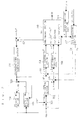
- FIG. 1 is a circuit diagram showing a converter, to which a converter control method according to an embodiment of the present invention is applied, and a configuration connected to the circumference thereof.
- a multi-phase power source I is a three-phase power source which outputs three-phase voltages of phases R, S, T.
- the number of phases is three, but the number of phases is not limited to three.
- the currents Ir, Is, It are inputted from the multi-phase power source I to a converter 3 via an EMI (Electro Magnetic Interference) filter and an input reactor group 2.
- the currents Ir, Is, It are line currents of the R phase, the S phase, and the T phase, respectively.
- the EMI filter removes a high-frequency noise and the like included in the currents Ir, Is, It.
- the input reactor group 2 prevents an inrush current from flowing into the converter 3, and moreover supports a potential difference between an input voltage of the converter 3 and an output voltage of the multi-phase power source 1.
- the converter 3 is a voltage-source PWM converter having a well-know switching element, and performs switching of the switching element, to output a DC voltage Vdc.
- the DC voltage Vdc is applied to the inverter 4, and a well-known inverter operation is performed so that three-phase currents Iu, Iv, Iw are outputted.
- the three-phase load 6 is supplied with the three-phase currents Iu, Iv, Iw, and driven.
- a motor is shown as an example of the three-phase load 6.
- the number of phases of the current outputted by the inverter 4 is not limited to three.
- a capacitor 5 which supports the DC voltage Vdc is provided in a DC link between the converter 3 and the inverter 4.
- the present invention is applicable to a converter employed in an AC-AC converter (in a broad sense) in which no capacitor 5 is provided.
- Switching in the converter 3 and the inverter 4 is controlled based on switching control signals Gcnv and Ginv, respectively.
- the switching control signals Gcnv and Ginv are generated by a converter waveform control section 7 and an inverter control section 8, respectively.
- the inverter control section 8 is generated based on a command value ⁇ m* of a drive frequency of the three-phase load 6, the DC voltage Vdc, and the three-phase currents Iu, Iv, Iw. This generation is a well-known technique and not directly related to the present invention, and therefore details thereof are omitted.
- FIG. 2 is a circuit diagram showing a conventional configuration employable as the converter waveform control section 7 of FIG. 1 .
- a switching control signal G0 is outputted as the switching control signal Genv.
- This configuration corresponds to a configuration obtained by simplifying the disclosure of the Patent Document 2.
- a voltage Vi which is an effective value per one phase of the voltage inputted to the converter 3 is represented by a pair of a d-axis voltage Vd and a q-axis voltage Vq,
- the square of the voltage Vi is equal to the sum of the square of the d-axis voltage Vd and the square of the q-axis voltage Vq.
- a phase computing section 708 determines a power supply phase ⁇ based on the zero-crossing signal ⁇ rs of the voltage between the R-S phases, and gives this to a phase converting section 707 and a PWM control section 709.
- the phase converting section 707 performs a three-phase/two-phase conversion into a d-axis-q-axis coordinate system which is the above-mentioned rotating coordinate system, and calculates a d-axis current Id and a q-axis current Iq which are a d-axis component and a q-axis component of the line currents Ir, Is, It.
- the d-axis current Id and the q-axis current Iq contribute to active power and reactive power, respectively. Therefore, to improve a power factor, it is desirable that the q-axis current Iq is small.
- the line current It is determined based on the line currents Ir, Is.
- an input of the line current It into the phase converting section 707 may be omitted, and in FIG. 2 , this omission is indicated by the reference character It being in parenthesis.
- An adder-subtractor 701 subtracts the DC voltage Vdc from a DC voltage command value Vdc*, to obtain a voltage deviation ⁇ Vdc.
- a PI control section 702 performs a PI control based on the voltage deviation ⁇ Vdc, to thereby obtain a d-axis current command value Id*,
- the d-axis current command value Id* corresponds to a command value of the d-axis current Id.
- An adder- subtractor 703 subtracts the d-axis current Id from the d-axis current command value Id*, to obtain a current deviation ⁇ Id.
- a PI control section 704 performs a PI control based on the current deviation ⁇ Id, to thereby obtain a d-axis voltage command value Vd*.
- the d-axis voltage command value Vd* corresponds to a command value of the d-axis voltage Vd.
- An adder-subtractor 705 subtracts the q-axis current Iq from a q-axis current command value Iq*, to obtain a current deviation ⁇ Id.
- the q-axis current command value Iq* corresponds to a command value of the q-axis current Id.
- a PI control section 706 performs a PI control based on the current deviation ⁇ Iq, to thereby obtain a q-axis voltage command value Vq*.
- the q-axis voltage command value Vq* corresponds to a command value of the q-axis voltage Vq.
- the d-axis voltage command value Vd*, the q-axis voltage command value Vq*, and the power supply phase ⁇ are inputted to the PWM control section 709, and the switching control signal G0 is generated based on them.
- the switching control signal G0 is used as the switching control signal Gcnv shown in FIG. 1 .
- the generation of the switching control signal G0 is performed using a well-known technique, and therefore a detailed description thereof is omitted.
- the voltage Vi inputted to the converter 3 is represented by ⁇ (Vd 2 +Vq 2 ), and therefore the voltage Vi is here estimated to be ⁇ (Vd *2 +Vq *2 ).
- the DC voltage Vdc is also given to the PWM control section 709, and a modulation rate Ks is obtained as ⁇ 2(Vi/Vdc).
- the voltage Vi is the effective value per one phase of the voltage inputted to the converter 3, and therefore the modulation rate Ks is a ratio of the crest value of the input voltage Vi with respect to the DC voltage Vdc.
- An adder-subtractor 721 subtracts, from the modulation rate Ks, its command value Ks*, and a resulting difference is subjected to a proportional computation in a proportional computation section 722, so that a deviation ⁇ K of the modulation rate is obtained.
- a multiplying section 723 multiplies the deviation ⁇ K by a coefficient ⁇ which adopts two values of 0 or 1.
- An integrator 724 integrates a multiplying result ⁇ K, to generate the DC voltage command value Vdc*.
- a restricting section 725 has the DC voltage command value Vdc* inputted thereto, and when this is within a desired range, outputs the value 1 as the coefficient ⁇ .
- the value 0 is adopted as the coefficient ⁇ if the deviation ⁇ K is negative, and the value 1 is adopted as the coefficient ⁇ if the deviation ⁇ K is positive.
- the value I is adopted as the coefficient ⁇ if the deviation ⁇ K is negative, and the value 0 is adopted as the coefficient ⁇ if the deviation ⁇ K is positive. In this manner, using a negative correlation between the DC voltage command value Vdc* and the modulation rate Ks, an excessive increase of an integrate value in the integrating section 724 is limited.
- FIG. 3 contains graphs showing operations of the respective sections of the configuration shown in FIG. 2 , in a case where a power source voltage instantaneously drops from 400V to 340V, and then recovers.
- a time of occurrence of the instantaneous voltage drop and a time of the recovery are indicated by times t0 and t1, respectively.
- the instantaneous voltage drop occurs and thus the absolute value of the d-axis current Id instantaneously drops (see the third graph from the top in FIG. 3 : a variation of the value -Id at the time t0 is rapid and indicated as a downward line in the graph).
- This variation of the d-axis current Id causes a steep drop of the d-axis voltage command value Vd* outputted by the PI control section 704 (the fourth graph from the top in FIG. 3 ). Since the computation in the PI control section 704 includes an integral term, a value s2 based on the integral term gently drops. However, ordinarily, the integral term has a small influence and a proportional term has a large influence in the PI control section 704. Therefore, the d-axis voltage command value Vd* is largely affected by the variation of the d-axis current Id, as described above.
- the steep drop of the d-axis voltage command value Vd* causes a steep drop of the voltage Vi. Since the drop of the DC voltage Vdc is slower than this steep drop of the voltage Vi, the modulation rate Ks rapidly drops (the first graph from the top in FIG. 3 ). Then, the DC voltage Vdc also drops (the second graph from the top in FIG. 3 ), and thereby the modulation rate Ks rises (the first graph from the top in FIG. 3 ).
- the deviation ⁇ K is negative, and the DC voltage command value Vdc* also gradually drops due to the function of the integrating section 724.
- the DC voltage command value Vdc* drops at a lower speed than the DC voltage Vdc does, and therefore the deviation ⁇ Vdc swings to the positive and the d-axis current command value Id* is lowered (the value -Id* rises). Then, the DC voltage command value Vdc* also decreases, and thus the deviation ⁇ Vdc becomes small (see the second graph from the top in FIG. 3 ).
- the d-axis current command value Id* outputted by the PI control section 702 rapidly increases (the value -Id* decreases), and the current deviation ⁇ Id becomes positive. Accordingly, the d-axis voltage command value Vd* outputted by the PI control section 704 increases. As described above, since the integral term has a small influence and the proportional term has a large influence in the PI control section 704, the d-axis voltage command value Vd* rapidly increases.
- the converter 3 operates as a buck-converting device with respect to the DC voltage Vdc, and therefore operates in a rectifier mode and the modulation rate Ks adopts the maximum value 1. Thereby, the deviation ⁇ K becomes positive.
- the DC voltage command value Vdc* slowly rises and then coincides with the DC voltage Vdc at a time t2.
- the value s1 based on the integral term is gently lowered.
- the DC voltage command value Vdc* continues to rise. Therefore, at or after the time t2, the deviation ⁇ Vdc becomes positive, and the value s1 slowly rises.
- the d-axis current command value Id* gently decreases (the value -Id* increases), and coincides with the d-axis current Id at a time t3. That is, until the time t3, the value s2 based on the integral term in the PI control section 704 continues to increase gently, and then decreases. However, as described above, the integral term has a small influence in the PI control section 704. Therefore, a timing at which the d-axis voltage command value Vd* adopts the local maximum value is earlier than the time t3 at which the value s2 adopts the local maximum value.
- the converter 3 Even when the deviation ⁇ Id becomes zero at the time t3, unless the d-axis voltage command value Vd* falls lower than the power source voltage 400V, the converter 3 operates in the rectifier mode and the modulation rate Ks continues to adopt the maximum value 1, as described above. Accordingly, the deviation ⁇ K is positive, and due to the function of the integrating section 724, the DC voltage command value Vdc* continues to increase and the d-axis current command value Id* continues to decrease gently (the value -Id* continues to increase).
- the d-axis voltage command value Vd* falls lower than 400V at a time t4, then the converter 3 recovers from the rectifier mode to a normal converter operation. Thereby, an overshoot occurs in the DC voltage Vdc, and an undershoot occurs in the modulation rate Ks. Moreover, since the value -Id* is lowered (the d-current command value Id* increases), the value -Id* is shown as an overshoot in FIG. 3 . While the DC voltage Vdc is recovering to the steady state, an overshoot occurs also in the value s1.
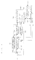
- FIG. 4 is a circuit diagram showing a configuration of a converter waveform control section according to a first embodiment, which is employable as the converter waveform control section 7 of FIG. 1 .
- a switching control signal G1 is outputted as the switching control signal Genv.
- adder-subtractors 701, 703, 705, PI control sections 702, 704, 706, a phase converting section 707, a phase computing section 708, and a PWM control section 709 employed in the converter waveform control section according to this embodiment those shown in FIG. 2 are employed.
- a voltage command value computing section 710 is employed instead of the adder-subtractor 721, the proportional computation section 722, the multiplying section 723, the integrator 724, and the restricting section 725 which are shown in FIG. 2 .
- the voltage command value computing section 710 generates the DC voltage command value Vdc* based on the d-axis voltage command value Vd* outputted from the PI control section 704, and gives this to the adder-subtractor 701. In this manner, the generation of the DC voltage command value Vdc* is based on the d-axis voltage command value Vd*.
- a power supply phase is required, a voltage itself of a multi-phase power source is not required. Accordingly, a circuit configuration for detecting a voltage of a multi-phase power source is not necessary, which makes it easy to control the DC voltage Vdc so as to improve a power factor while suppressing the size and the manufacturing costs.
- the DC voltage command value Vdc* is determined based on a value (Vd*-r ⁇ Id) obtained by subtracting from the d-axis voltage command value Vd* the product r ⁇ Id of at least a resistance component r of the reactor group 2 and the d-axis current Id.
- the value (Vd*-r ⁇ Id) is an estimate value of the power source voltage, and a control of the DC voltage Vdc substantially based on a power source voltage can be realized without actually measuring the power source voltage.
- the value of the resistance component r is stored in the voltage command value computing section 710 or inputted from the outside.
- the d-axis current Id can be obtained from the phase converting section 707.
- Vd Vs+(Ls+r)Id- ⁇ L ⁇ Iq
- Vd Vs+r ⁇ Id
- the d-axis voltage Vd and the power source voltage Vs are not measured. Therefore, using the d-axis voltage command value Vd* instead of the d-axis voltage Vd, the value (Vd*-r ⁇ Id) is treated as an estimate value of the power source voltage Vs.
- the DC voltage command value Vdc* may be determined based on a value (Vi-r ⁇ Id) obtained by subtracting at least the product r ⁇ Id from the voltage Vi (or its estimate value) inputted to the converter 3. Particularly when the phase difference ⁇ is small, the power source voltage Vs is substantially equal to the voltage Vi, and therefore such a determination may be performed.
- FIG. 5 contains graphs showing operations of the respective sections of the configuration shown in FIG. 4 , in a case where a power source voltage instantaneously drops from 400V to 340V, and then recovers. Similarly to FIG. 3 , a time of occurrence of the instantaneous voltage drop and a time of the recovery are indicated by times t0 and t1, respectively.
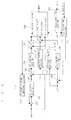
- FIG. 6 is a circuit diagram showing a configuration according to a second embodiment, which is employable as the converter waveform control section 7 of FIG. 1 .
- a switching control signal G2 is outputted as the switching control signal Gcnv.
- the configuration employed in the second embodiment has, in addition to the configuration employed in the first embodiment, voltage control sections 711, 713 and adders 712.714.
- the voltage control section 711 outputs, to the adder 712, a product ⁇ Ld ⁇ Id* of the d-axis current command value Id*, a d-axis inductance Ld of the reactor group 2, and an angular frequency ⁇ of the power source voltage.
- the voltage control section 713 outputs, to the adder 714, a product ⁇ Lq ⁇ Iq* of the q-axis current command value Iq*, a q-axis inductance Lq of the reactor group 2, and the angular frequency ⁇ .
- the d-axis inductance Ld and the q-axis inductance Lq are obtained by converting an inductance of the reactor group 2 into the d-axis-q-axis coordinate system.
- the adder 712 adds the product ⁇ Ld ⁇ Id* to an output of the PI control section 704, to generate the d-axis voltage command value Vd*.
- the adder 714 adds the product ⁇ Lq ⁇ Iq* to an output of the PI control section 706, to generate the q-axis voltage command value Vq*.
- the voltage control sections 711, 713 and the adders 712, 714 have a function to compensate for an interference term which is caused by the reactor group 2.
- the compensation itself for the interference term is a well-known technique, and thus a detailed description thereof is omitted.
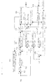
- FIG. 7 is a circuit diagram showing a configuration according to a third embodiment, which is employable as the converter waveform control section 7 of FIG. 1 .
- a switching control signal G3 is outputted as the switching control signal Genv.
- the configuration employed in the third embodiment is different from the configuration employed in the second embodiment, in that the voltage command value computing section 710 does not obtain the DC voltage command value Vdc* based on the d-axis voltage command value Vd*, but adopts an estimate value of the voltage Vi estimated to be ⁇ (Vd *2 +Vq *2 ) in the PWM control section 709.
- the voltage control sections 711, 713 and the adders 712, 714 may be omitted similarly to the first embodiment.
- the estimate of the voltage Vi may be obtained based on Vs/cos ⁇ .
- the DC voltage command value Vdc* may be set in the following manner.
- a product of the d-axis voltage command value Vd* and a constant ⁇ 2 ⁇ K1 is adopted as the DC voltage command value Vdc*.
- the constant K1 corresponds to the modulation rate Ks, and the modulation rate Ks can be kept constant even if the power source voltage varies.
- FIG. 8 is a block diagram illustrating a configuration of the voltage command value computing section 710
- FIG. 9 is a graph showing a relation between the DC voltage command value Vdc* and the power source voltage.
- the d-axis voltage command value Vd* is inputted to the proportional calculation section 710a, and the proportional calculation section 710a gives a product of the d-axis voltage command value Vd* and the constant ⁇ 2 ⁇ K1 to a limiter 710b.
- the limiter 710b slices the aforementioned product at a lower limit value Vdc_min and a upper limit value Vdc_max, and outputs it as the DC voltage command value Vdc*.
- the boosting rate can be kept constant.
- a value ( ⁇ 2 ⁇ Vd*+V1) obtained by adding a constant V1 to a product of the d-axis voltage command value Vd* and ⁇ 2 is adopted as the DC voltage command value Vdc*.
- a value ( ⁇ 2 ⁇ Vi+V1) obtained by adding the constant V1 to a product of ⁇ 2 and the estimate value Vi of the multi-phase voltage which is inputted to the converter 3 is adopted as the DC voltage command value Vdc*.
- the constant V1 gives a constant boosting to the DC voltage command value Vdc*. Therefore, as compared with the case where the proportional calculation indicated in (c-1) is adopted, a range of variation of the DC voltage command value Vdc*, which occurs when the power source voltage varies, can be restricted.
- FIG. 10 is a block diagram illustrating a configuration of the voltage command value computing section 710
- FIG. 11 is a graph showing a relation between the DC voltage command value Vdc* and the power source voltage.
- the d-axis voltage command value Vd* is inputted to the proportional calculation section 710c, and the proportional calculation section 710c multiplies the d-axis voltage command value Vd* by ⁇ 2 and gives a resultant to an adder 710d.
- the adder 710d adds the constant V1 to ⁇ 2 ⁇ Vd*, and gives a resultant to the limiter 710b.
- the limiter 710b slices the value (2 ⁇ Vd*+V1) at the lower limit value Vdc_min and the upper limit value Vdc_max, and outputs it as the DC voltage command value Vdc*.
- the d-axis voltage command value Vd* can be replaced with the estimate value Vi of the multi-phase voltage which is inputted to the converter 3.
- a value resulting from a K2-times multiplication of a value ( ⁇ 2 ⁇ Vd*+V2) obtained by adding a constant V2 to the product of the d-axis voltage command value Vd* and ⁇ 2 is adopted as the DC voltage command value Vdc*.
- a value resulting from a K2-times multiplication of a value ( ⁇ 2 ⁇ Vi+V2) obtained by adding the constant V2 to the product of ⁇ 2 and the estimate value Vi of the multi-phase voltage which is inputted to the converter 3 is adopted as the DC voltage command value Vdc*.
- FIG. 12 is a block diagram illustrating a configuration of the voltage command value computing section 710
- FIG. 13 is a graph showing a relation between the DC voltage command value Vdc* and the power source voltage.
- the d-axis voltage command value Vd* is inputted to the proportional calculation section 710c, and the proportional calculation section 710c multiplies the d-axis voltage command value Vd* by ⁇ 2 and gives a resultant to the adder 710d.
- the adder 710d adds the constant V2 to the value ⁇ 2 ⁇ Vd*, and gives a resultant to a multiplier 710e.
- the multiplier 710e gives the value ( ⁇ 2 ⁇ Vd*+V2) ⁇ K2 to the limiter 710b.
- the limiter 710b slices the value ( ⁇ 2 ⁇ Vd*+V2) ⁇ K2 at the lower limit value Vdc_min and the upper limit value Vdc_max, and outputs it as the DC voltage command value Vdc*.
- the d-axis voltage command value Vd* can be replaced with the estimate value Vi of the multi-phase voltage which is inputted to the converter 3.
- FIG. 14 is a block diagram illustrating a configuration of the voltage command value computing section 710.
- An average value computation section 710f obtains an average value of the d-axis voltage command value Vd* in a predetermined period.
- a proportional calculation section 710f multiplies this average value by a constant K3, and outputs the DC voltage command value Vdc*.
- FIG. 15 is a block diagram illustrating another configuration of the voltage command value computing section 710.
- a proportional calculation section 710h obtains a product of the d-axis voltage command value Vd* and a constant K4.
- a primary delay computation section 710i performs a primary delay computation on this product.
- a filter process for the d-axis voltage command value Vd* is performed, so that a high-frequency fluctuation component of the DC voltage command value Vdc* can be removed.
- a control system which is stable with respect to a transient response can be formed by making a response of the voltage command value computing section 710 for determining the DC voltage command value Vdc* sufficiently later than a response (specifically, responses of the PI control sections 702, 704) for obtaining the d-axis voltage command value Vd* based on the deviation ⁇ Vdc and a response (specifically, a response of the PI control section 706) for obtaining the q-axis voltage command value Vq*.
- the d-axis voltage command value Vd* may be replaced with the estimate value Vi of the multi-phase voltage which is inputted to the converter 3.
- the computation of the DC voltage command value Vd* may be changed in accordance with a command value J (see FIG. 1 ) from the inverter control section 8.
- a command value J see FIG. 1
- the inverter control section 8 causes the inverter 4 to perform a high-speed rotation driving of the motor, for example, to advance the current phase and perform a field-weakening control.
- the inverter control section 8 outputs the command value J, thereby controlling the operation of the converter waveform control section 7.
- the operation of the converter waveform control section 7 and consequently the operation of the converter 3, and the operation of the inverter control section 8 and consequently the operation of the inverter 4 cooperate with each other, and thereby the DC voltage Vdc can be set high only when a high-speed rotation of the motor is required.
- This enables expansion of the inverter operating range, by normally performing a high-efficiency control with suppressing of a boosting of the DC voltage Vdc and realizing a high-speed rotation only when needed.
Landscapes
- Engineering & Computer Science (AREA)
- Power Engineering (AREA)
- Inverter Devices (AREA)
- Rectifiers (AREA)
- Dc-Dc Converters (AREA)
- Control Of Ac Motors In General (AREA)
- Control Of Motors That Do Not Use Commutators (AREA)
Abstract
Description
- The present invention relates to a converter control method, and particularly to a method for controlling a converter which rectifies a multi-phase current.
- When a DC voltage is obtained by rectifying a current obtained from an AC power source, a higher power factor is desired. For example, in order to set a power factor at one in the use of a voltage-source PWM converter, it is necessary that an outputted DC voltage is set at a value higher than the peak value of an output voltage of the AC power source. If the specification of the output voltage of the AC power source in actual use is indefinite, the DC voltage is set to be a voltage relatively higher than the voltage according to the general specification.
- However, raising a set value of the DC voltage outputted from a converter means raising the maximum value of a voltage value given to an inverter device to which this DC voltage is inputted. This increases the loss of switching elements included in the converter and the inverter and the loss of a reactor interposed between the AC power source and the converter, which causes a problem that the efficiency of a converting device as a whole of a converter/inverter deteriorates.
- To avoid such a situation, a method has been proposed in which an output voltage of an AC power source is detected and a lower limit value of a voltage at which the DC voltage is to be set is adjusted to be a value higher than the peak value of the detected voltage (for example,
Patent Document 1 mentioned below). -
- Patent Document 1: Japanese Patent Application Laid-Open No.
7-245957 - Patent Document 2: Japanese Patent Application Laid-Open No
2006-6406 - However, this method requires a voltage detection circuit that detects the output voltage of the AC power source, which increases the size and the costs of a control circuit. Additionally, when a command value of the DC voltage is set, an error of the voltage detection circuit has to be considered, and it is difficult to limit a rise of the DC voltage to the minimum.
- On the other hand, a method has been also proposed in which the command value of the DC voltage is set such that there is no difference between a modulation rate of a PWM converter and a modulation rate command value (for example, the
Patent Document 2 mentioned above). In this method, the DC voltage can be controlled in accordance with a variation of the voltage of the AC power source, without the need to detect the output voltage of the AC power source. - However, in this method, in order to make the modulation rate coincident with the modulation rate command value, an integrator is required to compute the command value of the DC voltage. An integrator for obtaining a voltage command value used for a PWM control is also required. Thus, there is a problem that, in a case of a recovery after an instantaneous voltage drop, operations of the two kinds of integrators mentioned above interfere with each other to cause a overshoot of the DC voltage, as will be detailed later in a comparative example with respect to an embodiment of the present invention.
- An object of the present invention is to control a DC voltage in accordance with a variation of a power source voltage without the need to detect an effective value of the power source voltage. If this object is achieved, the reliability of the control is improved, and moreover the breakdown voltage of an element is reduced.
- In a preferred mode of the present invention, it is also an object to avoid an overshoot of a DC voltage in case of a recovery after an instantaneous voltage drop.
- A converter control method according to the present invention is a method of controlling a DC voltage (Vdc) in a converter (3) to which a multi-phase current (Ir, Is, It) is inputted from a multi-phase power source (1) and which performs switching to output the DC voltage (Vdc). A command value of the DC voltage is a DC voltage command value (Vdc*). A multi-phase voltage inputted to the converter is represented by a pair of a first voltage (Vd) and a second voltage (Vq) in a rotating coordinate system which rotates at a power-supply frequency (ω/2π) of the multi-phase power source. The second voltage has a phase advance of 90 degrees relative to the first voltage. Command values for the first voltage and the second voltage are a first voltage command value (Vd*) and a second voltage command value (Vq*), respectively.
- In a first aspect of the converter control method according to the present invention, a deviation (ΔVdc) of the DC voltage with respect to the DC voltage command value (Vdc*) is obtained, the switching is controlled based on the first voltage command value and the second voltage command value, and the DC voltage command value is determined based on the first voltage command value.
- For example, a square root of the sum of the square of the first voltage command value (Vd*) and the square of the second voltage command value (Vq*) is obtained as an estimate value of a voltage (Vi) of the multi-phase voltage which is inputted to the converter (3), and the DC voltage command value (Vdc*) is determined based on the estimate value.
- For example, a reactor group (2) in which the multi-phase current (Ir, Is, It) flows is provided between the multi-phase power source (1) and the converter (3). A value (Vd*-r·Id) is obtained as an estimate value of a voltage (Vs) of the multi-phase power source, the value (Vd*-r·Id) being obtained by subtracting, from the first voltage command value (Vd*), a product of at least a resistance component (r) of the reactor group which is represented in the rotating coordinate system and a component (Id) having the same phase as that of the first voltage of the multi-phase current which is represented in the rotating coordinate system. The DC voltage command value (Vdc*) is determined based on the estimate value.
- Alternatively, for example, a reactor group (2) in which the multi-phase current (Ir, Is, It) flows is provided between the multi-phase power source (1) and the converter (3). A value (Vi-r·Id) is obtained by subtracting a product of at least a resistance component (r) of the reactor group which is represented in the rotating coordinate system and a component (Id) having the same phase as that of the first voltage of the multi-phase current which is represented in the rotating coordinate system, from a voltage (Vi) of the multi-phase voltage which is inputted to the converter. The DC voltage command value (Vdc*) is determined based on the value.
- Alternatively, for example, a value (Vs/cosΨ) is obtained as an estimate value of the multi-phase voltage (Vi) which is inputted to the converter, the value (Vs/cosΨ) being obtained by dividing an estimate value of a voltage (Vs) of the multi-phase power source by a cosine value (cosΨ) of an arc tangent (Ψ=tan-1(Vq*/Vd*)) of a value resulting from the second voltage command value (Vq*) being divided by the first voltage command value (Vd*). The DC voltage command value (Vdc*) is determined based on the estimate value.
- A second aspect of the converter control method according to the present invention is the first aspect thereof, in which a foodback loop including an integral element is removed from a determination of the DC voltage command value (Vdc*).
- In the first and second aspects, for example, a linear calculation for the first voltage command value, an estimate value of the multi-phase voltage (Vi) which is inputted to the converter, or an estimate value of the voltage (Vs) of the multi-phase power source, is adopted for a determination of the DC voltage command value (Vdc*).
- A third aspect of the converter control method according to the present invention is the second aspect thereof, in which a constant used in the calculation mentioned above is set in cooperation with an operation of an inverter (4) to which the DC voltage (Vdc) is inputted.
- A fourth aspect of the converter control method according to the present invention is the first aspect or the second aspect thereof, including a filter process for the first voltage command value (Vd*), an estimate value of the multi-phase voltage (Vi) which is inputted to the converter (3), or an estimate value of the voltage (Vs) of the multi-phase power source.
- In the first aspect of the converter control method according to the present invention, a power supply phase of the multi-phase power source is required, but a voltage of the multi-phase power source is not required. Therefore, a circuit configuration for detecting a voltage of the multi-phase power source is not necessary, which makes it easy to control the DC voltage so as to improve a power factor of input power while suppressing the size and manufacturing costs.
- In the second aspect of the converter control method according to the present invention, a time delay element such as the integral element is not included in the determination of the DC voltage command value. Accordingly, this determination is not delayed due to an instantaneous stop / recovery. Thus, occurrence of an overshoot of the DC voltage based on this delay can be avoided.
- In the third aspect of the converter control method according to the present invention, the DC voltage can be set in accordance with driving of a load of the inverter. Therefore, an operating range of the inverter can be expanded.
- In the fourth aspect of the converter control method according to the present invention, a primary delay element and the filter process such as an average computation are included in the determination of the DC voltage command value, and thereby a response of a control system which determines the DC voltage command value is made later than a response of a control system which determines the first voltage command value and the second voltage command value, so that a control which is stable with respect to a transient response is performed.
- These and other objects, features, aspects and advantages of the present invention will become more apparent from the following detailed description of the present invention when taken in conjunction with the accompanying drawings.
-
- [
FIG. 1 ] A circuit diagram showing a converter, to which a converter control method according to an embodiment of the present invention is applied, and a configuration connected to the circumference thereof. - [
FIG. 2 ] A circuit diagram showing a configuration of a conventional converter waveform control section. - [
FIG. 3 ] A graph showing an operation of the conventional converter waveform control section. - [
FIG. 4 ] A circuit diagram showing a configuration of a converter waveform control section according to a first embodiment of the present invention. - [
FIG. 5 ] A graph showing an operation of the converter waveform control section according to the first embodiment of the present invention. - [
FIG. 6 ] A circuit diagram showing a configuration of a converter waveform control section according to a second embodiment of the present invention. - [
FIG. 7 ] A circuit diagram showing a configuration of a converter waveform control section according to a third embodiment of the present invention. - [
FIG. 8 ] A block diagram illustrating a configuration of a voltage command value computing section. - [
FIG. 9 ] A graph showing a relation between a DC voltage command value and a power source voltage. - [
FIG. 10 ] A block diagram illustrating another configuration of the voltage command value computing section. - [
FIG. 11 ] A graph showing a relation between a DC voltage command value and a power source voltage. - [
FIG. 12 ] A block diagram illustrating still another configuration of the voltage command value computing section. - [
FIG. 13 ] A graph showing a relation between a DC voltage command value and a power source voltage. - [
FIG. 14 ] A block diagram illustrating still another configuration of the voltage command value computing section. - [
FIG. 15 ] A block diagram illustrating still another configuration of the voltage command value computing section. - In the following, as is often the case in this field, a current and its value are denoted by the same reference character. For example, the expression of "current I" is used for representing both a current I flowing in a circuit and its value. The same applies to a voltage and other various amounts.
-
FIG. 1 is a circuit diagram showing a converter, to which a converter control method according to an embodiment of the present invention is applied, and a configuration connected to the circumference thereof. - A multi-phase power source I is a three-phase power source which outputs three-phase voltages of phases R, S, T. In this embodiment, the number of phases is three, but the number of phases is not limited to three.
- Currents Ir, Is, It are inputted from the multi-phase power source I to a
converter 3 via an EMI (Electro Magnetic Interference) filter and aninput reactor group 2. The currents Ir, Is, It are line currents of the R phase, the S phase, and the T phase, respectively. The EMI filter removes a high-frequency noise and the like included in the currents Ir, Is, It. Theinput reactor group 2 prevents an inrush current from flowing into theconverter 3, and moreover supports a potential difference between an input voltage of theconverter 3 and an output voltage of themulti-phase power source 1. - The
converter 3 is a voltage-source PWM converter having a well-know switching element, and performs switching of the switching element, to output a DC voltage Vdc. - The DC voltage Vdc is applied to the
inverter 4, and a well-known inverter operation is performed so that three-phase currents Iu, Iv, Iw are outputted. The three-phase load 6 is supplied with the three-phase currents Iu, Iv, Iw, and driven. Here, a motor is shown as an example of the three-phase load 6. The number of phases of the current outputted by theinverter 4 is not limited to three. - A capacitor 5 which supports the DC voltage Vdc is provided in a DC link between the
converter 3 and theinverter 4. However, the present invention is applicable to a converter employed in an AC-AC converter (in a broad sense) in which no capacitor 5 is provided. - Switching in the
converter 3 and theinverter 4 is controlled based on switching control signals Gcnv and Ginv, respectively. The switching control signals Gcnv and Ginv are generated by a converter waveform control section 7 and aninverter control section 8, respectively. - The
inverter control section 8 is generated based on a command value ωm* of a drive frequency of the three-phase load 6, the DC voltage Vdc, and the three-phase currents Iu, Iv, Iw. This generation is a well-known technique and not directly related to the present invention, and therefore details thereof are omitted. - The converter waveform control section 7 is generated based on a zero-crossing signal ϕrs of a voltage between R-S phases in the
multi-phase power source 1, the line currents Ir, Is, It, and the DC voltage Vdc. Generally, there is the relation of It = -(Is+Ir). Therefore, in the configuration shown inFIG. 1 , the line currents Ir, Is are obtained by current transformers CT1, CT2, respectively, and these are given to the converter waveform control section 7. - Before a description of an operation of the converter waveform control section 7 employed in this embodiment, a control method of a conventional converter will be described and problems thereof will be detailed firstly. Then, the fact that these problems are solved by the operation of the converter waveform control section 7 employed in this embodiment will be described.
-
FIG. 2 is a circuit diagram showing a conventional configuration employable as the converter waveform control section 7 ofFIG. 1 . In this configuration, a switching control signal G0 is outputted as the switching control signal Genv. This configuration corresponds to a configuration obtained by simplifying the disclosure of thePatent Document 2. - Here, introduced is an expression using a d-axis and a q-axis employed in a rotating coordinate system which rotates at a power-supply frequency (ω/2π) of the
multi-phase power source 1. The q-axis has a phase advance of 90 degrees relative to the d-axis. For example, a voltage Vi, which is an effective value per one phase of the voltage inputted to theconverter 3, is represented by a pair of a d-axis voltage Vd and a q-axis voltage Vq, To be more specific, the square of the voltage Vi is equal to the sum of the square of the d-axis voltage Vd and the square of the q-axis voltage Vq. - A
phase computing section 708 determines a power supply phase θ based on the zero-crossing signal ϕrs of the voltage between the R-S phases, and gives this to aphase converting section 707 and aPWM control section 709. - In accordance with the power supply phase θ, the
phase converting section 707 performs a three-phase/two-phase conversion into a d-axis-q-axis coordinate system which is the above-mentioned rotating coordinate system, and calculates a d-axis current Id and a q-axis current Iq which are a d-axis component and a q-axis component of the line currents Ir, Is, It. The d-axis current Id and the q-axis current Iq contribute to active power and reactive power, respectively. Therefore, to improve a power factor, it is desirable that the q-axis current Iq is small. - As described above, the line current It is determined based on the line currents Ir, Is. Thus, an input of the line current It into the
phase converting section 707 may be omitted, and inFIG. 2 , this omission is indicated by the reference character It being in parenthesis. - An adder-
subtractor 701 subtracts the DC voltage Vdc from a DC voltage command value Vdc*, to obtain a voltage deviation ΔVdc. - A
PI control section 702 performs a PI control based on the voltage deviation ΔVdc, to thereby obtain a d-axis current command value Id*, The d-axis current command value Id* corresponds to a command value of the d-axis current Id. - An adder-
subtractor 703 subtracts the d-axis current Id from the d-axis current command value Id*, to obtain a current deviation ΔId. - A
PI control section 704 performs a PI control based on the current deviation ΔId, to thereby obtain a d-axis voltage command value Vd*. The d-axis voltage command value Vd* corresponds to a command value of the d-axis voltage Vd. - An adder-
subtractor 705 subtracts the q-axis current Iq from a q-axis current command value Iq*, to obtain a current deviation ΔId. The q-axis current command value Iq* corresponds to a command value of the q-axis current Id. - A
PI control section 706 performs a PI control based on the current deviation ΔIq, to thereby obtain a q-axis voltage command value Vq*. The q-axis voltage command value Vq* corresponds to a command value of the q-axis voltage Vq. - The d-axis voltage command value Vd*, the q-axis voltage command value Vq*, and the power supply phase θ are inputted to the
PWM control section 709, and the switching control signal G0 is generated based on them. The switching control signal G0 is used as the switching control signal Gcnv shown inFIG. 1 . The generation of the switching control signal G0 is performed using a well-known technique, and therefore a detailed description thereof is omitted. - As described above, the voltage Vi inputted to the
converter 3 is represented by √(Vd2+Vq2), and therefore the voltage Vi is here estimated to be √(Vd*2+Vq*2). A phase difference between the voltage Vi and a power source voltage Vs is represented by Ψ=tan-1 (Vq*/Vd*). - Furthermore, the DC voltage Vdc is also given to the
PWM control section 709, and a modulation rate Ks is obtained as √2(Vi/Vdc). As described above, the voltage Vi is the effective value per one phase of the voltage inputted to theconverter 3, and therefore the modulation rate Ks is a ratio of the crest value of the input voltage Vi with respect to the DC voltage Vdc. - An adder-
subtractor 721 subtracts, from the modulation rate Ks, its command value Ks*, and a resulting difference is subjected to a proportional computation in aproportional computation section 722, so that a deviation ΔK of the modulation rate is obtained. A multiplyingsection 723 multiplies the deviation ΔK by a coefficient ε which adopts two values of 0 or 1. Anintegrator 724 integrates a multiplying result ε·ΔK, to generate the DC voltage command value Vdc*. - A restricting
section 725 has the DC voltage command value Vdc* inputted thereto, and when this is within a desired range, outputs thevalue 1 as the coefficient ε. When the DC voltage command value Vdc* is smaller than the desired range, the value 0 is adopted as the coefficient ε if the deviation ΔK is negative, and thevalue 1 is adopted as the coefficient ε if the deviation ΔK is positive. When the DC voltage command value Vdc* is larger than the desired range, the value I is adopted as the coefficient ε if the deviation ΔK is negative, and the value 0 is adopted as the coefficient ε if the deviation ΔK is positive. In this manner, using a negative correlation between the DC voltage command value Vdc* and the modulation rate Ks, an excessive increase of an integrate value in the integratingsection 724 is limited. -
FIG. 3 contains graphs showing operations of the respective sections of the configuration shown inFIG. 2 , in a case where a power source voltage instantaneously drops from 400V to 340V, and then recovers. Here, a time of occurrence of the instantaneous voltage drop and a time of the recovery are indicated by times t0 and t1, respectively. - Here, a case is considered where the d-axis current command value Id* is negative in a steady state. In the graphs, values -Id* and -Id, which are obtained by changing the signs of the d-axis current command value Id* and the d-axis current Id, respectively, are indicated.
- At the time t0, the instantaneous voltage drop occurs and thus the absolute value of the d-axis current Id instantaneously drops (see the third graph from the top in
FIG. 3 : a variation of the value -Id at the time t0 is rapid and indicated as a downward line in the graph). - This variation of the d-axis current Id causes a steep drop of the d-axis voltage command value Vd* outputted by the PI control section 704 (the fourth graph from the top in
FIG. 3 ). Since the computation in thePI control section 704 includes an integral term, a value s2 based on the integral term gently drops. However, ordinarily, the integral term has a small influence and a proportional term has a large influence in thePI control section 704. Therefore, the d-axis voltage command value Vd* is largely affected by the variation of the d-axis current Id, as described above. - The steep drop of the d-axis voltage command value Vd* causes a steep drop of the voltage Vi. Since the drop of the DC voltage Vdc is slower than this steep drop of the voltage Vi, the modulation rate Ks rapidly drops (the first graph from the top in
FIG. 3 ). Then, the DC voltage Vdc also drops (the second graph from the top inFIG. 3 ), and thereby the modulation rate Ks rises (the first graph from the top inFIG. 3 ). - Since the modulation rate Ks drops relative to the modulation rate command value Ks*, the deviation ΔK is negative, and the DC voltage command value Vdc* also gradually drops due to the function of the integrating
section 724. However, immediately after the time t0, the DC voltage command value Vdc* drops at a lower speed than the DC voltage Vdc does, and therefore the deviation ΔVdc swings to the positive and the d-axis current command value Id* is lowered (the value -Id* rises). Then, the DC voltage command value Vdc* also decreases, and thus the deviation ΔVdc becomes small (see the second graph from the top inFIG. 3 ). - The power source recovers at the time t1, then the DC voltage Vdc is charged to approximately 565V which is the peak value of the power source voltage. However, since the DC voltage command value Vdc* increases due to the integration computation in the integrating
section 724, the speed of the increase is low. Therefore, the deviation ΔVdc suddenly becomes negative at the time t1 - Thus, the d-axis current command value Id* outputted by the
PI control section 702 rapidly increases (the value -Id* decreases), and the current deviation ΔId becomes positive. Accordingly, the d-axis voltage command value Vd* outputted by thePI control section 704 increases. As described above, since the integral term has a small influence and the proportional term has a large influence in thePI control section 704, the d-axis voltage command value Vd* rapidly increases. - Thereby, the voltage vi rapidly rises, and the modulation rate Ks reaches the
upper limit value 1. Here, theconverter 3 operates as a buck-converting device with respect to the DC voltage Vdc, and therefore operates in a rectifier mode and the modulation rate Ks adopts themaximum value 1. Thereby, the deviation ΔK becomes positive. - Since the deviation ΔK is positive, due to the integration computation in the integrating
section 724, the DC voltage command value Vdc* slowly rises and then coincides with the DC voltage Vdc at a time t2. In the same manner, in a period of the times t1 to t2. due to the integrating operation of the deviation ΔVdc (<0) in thePI control section 702, the value s1 based on the integral term is gently lowered. However, after the time t2, the DC voltage command value Vdc* continues to rise. Therefore, at or after the time t2, the deviation ΔVdc becomes positive, and the value s1 slowly rises. - Due to the slow increase of the DC voltage command value Vdc*, the d-axis current command value Id* gently decreases (the value -Id* increases), and coincides with the d-axis current Id at a time t3. That is, until the time t3, the value s2 based on the integral term in the
PI control section 704 continues to increase gently, and then decreases. However, as described above, the integral term has a small influence in thePI control section 704. Therefore, a timing at which the d-axis voltage command value Vd* adopts the local maximum value is earlier than the time t3 at which the value s2 adopts the local maximum value. - Even when the deviation ΔId becomes zero at the time t3, unless the d-axis voltage command value Vd* falls lower than the power source voltage 400V, the
converter 3 operates in the rectifier mode and the modulation rate Ks continues to adopt themaximum value 1, as described above. Accordingly, the deviation ΔK is positive, and due to the function of the integratingsection 724, the DC voltage command value Vdc* continues to increase and the d-axis current command value Id* continues to decrease gently (the value -Id* continues to increase). - The d-axis voltage command value Vd* falls lower than 400V at a time t4, then the
converter 3 recovers from the rectifier mode to a normal converter operation. Thereby, an overshoot occurs in the DC voltage Vdc, and an undershoot occurs in the modulation rate Ks. Moreover, since the value -Id* is lowered (the d-current command value Id* increases), the value -Id* is shown as an overshoot inFIG. 3 . While the DC voltage Vdc is recovering to the steady state, an overshoot occurs also in the value s1. - Then, the operations of the respective sections are stabilized at a time t5.
-
FIG. 4 is a circuit diagram showing a configuration of a converter waveform control section according to a first embodiment, which is employable as the converter waveform control section 7 ofFIG. 1 . In this configuration, a switching control signal G1 is outputted as the switching control signal Genv. - As adder-
subtractors PI control sections phase converting section 707, aphase computing section 708, and aPWM control section 709 employed in the converter waveform control section according to this embodiment, those shown inFIG. 2 are employed. - In this configuration, a voltage command
value computing section 710 is employed instead of the adder-subtractor 721, theproportional computation section 722, the multiplyingsection 723, theintegrator 724, and the restrictingsection 725 which are shown inFIG. 2 . - The voltage command
value computing section 710 generates the DC voltage command value Vdc* based on the d-axis voltage command value Vd* outputted from thePI control section 704, and gives this to the adder-subtractor 701. In this manner, the generation of the DC voltage command value Vdc* is based on the d-axis voltage command value Vd*. Although a power supply phase is required, a voltage itself of a multi-phase power source is not required. Accordingly, a circuit configuration for detecting a voltage of a multi-phase power source is not necessary, which makes it easy to control the DC voltage Vdc so as to improve a power factor while suppressing the size and the manufacturing costs. - Particularly, when a control for making a q-current Iq zero is performed, it is desirable that the DC voltage command value Vdc* is determined based on a value (Vd*-r·Id) obtained by subtracting from the d-axis voltage command value Vd* the product r·Id of at least a resistance component r of the
reactor group 2 and the d-axis current Id. This is because, based on the definition of the d-axis mentioned above, in the steady state, the value (Vd*-r·Id) is an estimate value of the power source voltage, and a control of the DC voltage Vdc substantially based on a power source voltage can be realized without actually measuring the power source voltage. In this case, it is desirable that the value of the resistance component r is stored in the voltage commandvalue computing section 710 or inputted from the outside. The d-axis current Id can be obtained from thephase converting section 707. - To indicate this in more detail using a mathematical formula, generally, Vd = Vs+(Ls+r)Id-ωL·Iq, and Vq = (Ls+r)Iq+ωL·Id are satisfied, where it is assumed that Ld = Lq = L for the sake of simplification and a power source voltage Vs and a differential operator s are introduced. Iq=0 (the q-current Iq is zero) is substituted into the first formula, and in the steady state, a computation result due to the differential operator s becomes zero. Thus, Vd = Vs+r·Id is obtained, and Vs = Vd-r·Id is satisfied. In this embodiment, the d-axis voltage Vd and the power source voltage Vs are not measured. Therefore, using the d-axis voltage command value Vd* instead of the d-axis voltage Vd, the value (Vd*-r·Id) is treated as an estimate value of the power source voltage Vs.
- Here, the DC voltage command value Vdc* may be determined based on a value (Vi-r·Id) obtained by subtracting at least the product r·Id from the voltage Vi (or its estimate value) inputted to the
converter 3. Particularly when the phase difference Ψ is small, the power source voltage Vs is substantially equal to the voltage Vi, and therefore such a determination may be performed. - It is desirable that a foodback loop including an integral element is removed from the determination of the DC voltage command value Vdc*. In this case, this determination is not delayed due to an instantaneous stop / recovery. Thus, occurrence of an overshoot of the DC voltage Vdc based on this delay can be avoided.
-
FIG. 5 contains graphs showing operations of the respective sections of the configuration shown inFIG. 4 , in a case where a power source voltage instantaneously drops from 400V to 340V, and then recovers. Similarly toFIG. 3 , a time of occurrence of the instantaneous voltage drop and a time of the recovery are indicated by times t0 and t1, respectively. - Here, a case is shown where the DC voltage command value Vdc* is set such that the d-axis voltage command value Vd* is multiplied by a predetermined coefficient and the same modulation rate Ks as shown in
FIG. 3 can be obtained. - Unlike the operation described in (b-1), there is no integrating operation in the integrating
section 724, and after the time t1, the d-axis voltage command value Vd* and the DC voltage command value Vdc* steeply change. Accordingly, the decrease of the d-axis current command value Id* (the increase of the value -Id*), which is observed in a period of times t1 to t4 ofFIG. 3 , occurs in a very short period. Therefore, no undershoot occurs in the modulation rate Ks, and the operations of the respective sections are stabilized at the time t6. -
FIG. 6 is a circuit diagram showing a configuration according to a second embodiment, which is employable as the converter waveform control section 7 ofFIG. 1 . In this configuration, a switching control signal G2 is outputted as the switching control signal Gcnv. - The configuration employed in the second embodiment has, in addition to the configuration employed in the first embodiment,
voltage control sections - The
voltage control section 711 outputs, to theadder 712, a product ωLd·Id* of the d-axis current command value Id*, a d-axis inductance Ld of thereactor group 2, and an angular frequency ω of the power source voltage. Thevoltage control section 713 outputs, to theadder 714, a product ωLq·Iq* of the q-axis current command value Iq*, a q-axis inductance Lq of thereactor group 2, and the angular frequency ω. The d-axis inductance Ld and the q-axis inductance Lq are obtained by converting an inductance of thereactor group 2 into the d-axis-q-axis coordinate system. Here, it is assumed that the values of respective reactors included in thereactor group 2 are equal to one another. - The angular frequency ω is obtained from a power-supply frequency f (ω=2πf). It is desirable that the value of the power-supply frequency f is stored in the voltage command
value computing section 710 or inputted from the outside (calculated from the zero-crossing signal ϕrs). The inputs of the angular frequency ω into thevoltage control sections - The
adder 712 adds the product ωLd·Id* to an output of thePI control section 704, to generate the d-axis voltage command value Vd*. Theadder 714 adds the product ωLq·Iq* to an output of thePI control section 706, to generate the q-axis voltage command value Vq*. In other words, thevoltage control sections adders reactor group 2. The compensation itself for the interference term is a well-known technique, and thus a detailed description thereof is omitted. -
FIG. 7 is a circuit diagram showing a configuration according to a third embodiment, which is employable as the converter waveform control section 7 ofFIG. 1 . In this configuration, a switching control signal G3 is outputted as the switching control signal Genv. - The configuration employed in the third embodiment is different from the configuration employed in the second embodiment, in that the voltage command
value computing section 710 does not obtain the DC voltage command value Vdc* based on the d-axis voltage command value Vd*, but adopts an estimate value of the voltage Vi estimated to be √(Vd*2+Vq*2) in thePWM control section 709. - Needless to say, in this embodiment as well, the
voltage control sections adders - Considering that there is the above-mentioned phase difference Ψ between the power source voltage Vs (an estimate value thereof) and the voltage Vi, the estimate of the voltage Vi may be obtained based on Vs/cosΨ.
- Specifically, the DC voltage command value Vdc* may be set in the following manner.
- For example, a product of the d-axis voltage command value Vd* and a
constant √ 2·K1 is adopted as the DC voltage command value Vdc*. In this case, a constant K1 corresponds to a boosting rate in a case of no load (Id=0), and this boosting rate can be kept constant even if the power source voltage varies. - Alternatively, a product of the
constant √ 2·KI and the estimate value Vi of the multi-phase voltage which is inputted to theconverter 3 is adopted as the DC voltage command value Vdc*. In this case, the constant K1 corresponds to the modulation rate Ks, and the modulation rate Ks can be kept constant even if the power source voltage varies. - However, it is actually desirable to set upper limit / lower limit of the DC voltage command value Vdc*.
FIG. 8 is a block diagram illustrating a configuration of the voltage commandvalue computing section 710, andFIG. 9 is a graph showing a relation between the DC voltage command value Vdc* and the power source voltage. - The d-axis voltage command value Vd* is inputted to the
proportional calculation section 710a, and theproportional calculation section 710a gives a product of the d-axis voltage command value Vd* and theconstant √ 2·K1 to alimiter 710b. Thelimiter 710b slices the aforementioned product at a lower limit value Vdc_min and a upper limit value Vdc_max, and outputs it as the DC voltage command value Vdc*. In a power-source-voltage range (Vac_min to Vac_max) which allows the DC voltage command value Vdc* to have a value between the lower limit value Vdc_min and the upper limit value Vdc_max, the boosting rate can be kept constant. - In
FIGS. 8 and 9 , if the d-axis voltage command value Vd* is replaced with the estimate value Vi of the multi-phase voltage which is inputted to theconverter 3, the modulation rate is kept constant in the power-source-voltage range (Vac_min to Vac_max). - For example, a value (√2·Vd*+V1) obtained by adding a constant V1 to a product of the d-axis voltage command value Vd* and √2 is adopted as the DC voltage command value Vdc*. Alternatively, a value (√2·Vi+V1) obtained by adding the constant V1 to a product of √2 and the estimate value Vi of the multi-phase voltage which is inputted to the
converter 3 is adopted as the DC voltage command value Vdc*. - In this case, the constant V1 gives a constant boosting to the DC voltage command value Vdc*. Therefore, as compared with the case where the proportional calculation indicated in (c-1) is adopted, a range of variation of the DC voltage command value Vdc*, which occurs when the power source voltage varies, can be restricted.
-
FIG. 10 is a block diagram illustrating a configuration of the voltage commandvalue computing section 710, andFIG. 11 is a graph showing a relation between the DC voltage command value Vdc* and the power source voltage. - The d-axis voltage command value Vd* is inputted to the
proportional calculation section 710c, and theproportional calculation section 710c multiplies the d-axis voltage command value Vd* by √2 and gives a resultant to anadder 710d. Theadder 710d adds the constant V1 to √2·Vd*, and gives a resultant to thelimiter 710b. Thelimiter 710b slices the value (2·Vd*+V1) at the lower limit value Vdc_min and the upper limit value Vdc_max, and outputs it as the DC voltage command value Vdc*. InFIGs. 10 and 11 , the d-axis voltage command value Vd* can be replaced with the estimate value Vi of the multi-phase voltage which is inputted to theconverter 3. - Alternatively, for example, a value resulting from a K2-times multiplication of a value (√2·Vd*+V2) obtained by adding a constant V2 to the product of the d-axis voltage command value Vd* and √2 is adopted as the DC voltage command value Vdc*. Alternatively, a value resulting from a K2-times multiplication of a value (√2·Vi+V2) obtained by adding the constant V2 to the product of √2 and the estimate value Vi of the multi-phase voltage which is inputted to the
converter 3 is adopted as the DC voltage command value Vdc*. - Since the transformation of (√2·Vd*+V2)×K2 = √2·Vd*×K2+V2×K2 = √2·Vd*×K1+V1 is possible, it can be seen that a range of change of the DC voltage Vdc can be reduced while the value of K1 is made constant to suppress a boost of the DC voltage Vdc. This is desirable, from the viewpoint of avoiding a situation where when the DC voltage Vdc drops, an operating range of the
inverter 4 cannot be fulfilled because of the drop. -
FIG. 12 is a block diagram illustrating a configuration of the voltage commandvalue computing section 710, andFIG. 13 is a graph showing a relation between the DC voltage command value Vdc* and the power source voltage. - The d-axis voltage command value Vd* is inputted to the
proportional calculation section 710c, and theproportional calculation section 710c multiplies the d-axis voltage command value Vd* by √2 and gives a resultant to theadder 710d. Theadder 710d adds the constant V2 to the value √2·Vd*, and gives a resultant to amultiplier 710e. Themultiplier 710e gives the value (√2·Vd*+V2)×K2 to thelimiter 710b. Thelimiter 710b slices the value (√2·Vd*+V2)×K2 at the lower limit value Vdc_min and the upper limit value Vdc_max, and outputs it as the DC voltage command value Vdc*. InFIGs. 12 and 13 , the d-axis voltage command value Vd* can be replaced with the estimate value Vi of the multi-phase voltage which is inputted to theconverter 3. -
FIG. 14 is a block diagram illustrating a configuration of the voltage commandvalue computing section 710. An averagevalue computation section 710f obtains an average value of the d-axis voltage command value Vd* in a predetermined period. Aproportional calculation section 710f multiplies this average value by a constant K3, and outputs the DC voltage command value Vdc*. -
FIG. 15 is a block diagram illustrating another configuration of the voltage commandvalue computing section 710. Aproportional calculation section 710h obtains a product of the d-axis voltage command value Vd* and a constant K4. A primarydelay computation section 710i performs a primary delay computation on this product. - In both of the two kinds of configurations described above, a filter process for the d-axis voltage command value Vd* is performed, so that a high-frequency fluctuation component of the DC voltage command value Vdc* can be removed. A control system which is stable with respect to a transient response can be formed by making a response of the voltage command
value computing section 710 for determining the DC voltage command value Vdc* sufficiently later than a response (specifically, responses of thePI control sections 702, 704) for obtaining the d-axis voltage command value Vd* based on the deviation ΔVdc and a response (specifically, a response of the PI control section 706) for obtaining the q-axis voltage command value Vq*. The d-axis voltage command value Vd* may be replaced with the estimate value Vi of the multi-phase voltage which is inputted to theconverter 3. - From the viewpoint of avoiding the overshoot and the undershoot described in (b-1), it is not desirable to obtain the DC voltage command value Vdc* with an integration calculation. However, it is possible to control the DC voltage Vdc in accordance with a variation of the power source voltage without the need to detect an effective value of the power source voltage.
- The computation of the DC voltage command value Vd* may be changed in accordance with a command value J (see
FIG. 1 ) from theinverter control section 8. To be specific, for example, when the three-phase load 6 is a motor and there is a need to rotate the motor at a high speed, theinverter 4 should be driven so as to fulfill the need. For such a driving, theinverter control section 8 causes theinverter 4 to perform a high-speed rotation driving of the motor, for example, to advance the current phase and perform a field-weakening control. When theinverter 4 is caused to perform such a high-speed rotation driving, theinverter control section 8 outputs the command value J, thereby controlling the operation of the converter waveform control section 7. - More specifically, which of the proportional calculation, the linear calculation, and the integration calculation illustrating in the above section "C" is adopted in the operation of the voltage command
value computing section 710 is determined, and furthermore the proportional constants K1, K2, V1, and V2 are set. - The operation of the converter waveform control section 7 and consequently the operation of the
converter 3, and the operation of theinverter control section 8 and consequently the operation of theinverter 4 cooperate with each other, and thereby the DC voltage Vdc can be set high only when a high-speed rotation of the motor is required. This enables expansion of the inverter operating range, by normally performing a high-efficiency control with suppressing of a boosting of the DC voltage Vdc and realizing a high-speed rotation only when needed. - While the invention has been described in detail, the foregoing description is in all aspects illustrative and not restrictive. It is therefore understood that numerous modifications and variations can be devised without departing from the scope of the invention.
Claims (9)
- A converter control method of controlling a DC voltage (Vdc) in a converter (3) to which a multi-phase current (Ir, Is, It) is inputted from a multi-phase power source (1) and which performs switching to output said DC voltage (Vdc), wherein
a command value of said DC voltage is a DC voltage command value (Vdc*),
a multi-phase voltage inputted to said converter is represented by a pair of a first voltage (Vd) and a second voltage (Vq) in a rotating coordinate system which rotates at a power-supply frequency (ω/2π) of said multi-phase power source,
said second voltage has a phase advance of 90 degrees relative to said first voltage,
command values for said first voltage and said second voltage are a first voltage command value (Vd*) and a second voltage command value (Vq*), respectively,
a deviation (ΔVdc) of said DC voltage with respect to said DC voltage command value (Vdc*) is obtained,
said switching is controlled based on said first voltage command value and said second voltage command value,
said DC voltage command value is determined based on said first voltage command value. - The converter control method according to claim 1, wherein
a square root of the sum of the square of said first voltage command value (Vd*) and the square of said second voltage command value (Vq*) is obtained as an estimate value of a voltage (Vi) of said multi-phase voltage which is inputted to said converter (3), and said DC voltage command value (Vdc*) is determined based on said estimate value. - The converter control method according to claim 1, wherein
a reactor group (2) in which said multi-phase current (Ir, Is, It) flows is provided between said multi-phase power source (1) and said converter (3),
a value (Vd*-r·Id) is obtained as an estimate value of a voltage (Vs) of said multi-phase power source, said value (Vd*-r·Id) being obtained by subtracting, from said first voltage command value (Vd*), a product (r·Id) of a resistance component (r) of said reactor group which is represented in said rotating coordinate system and a component (Id) having the same phase as that of said first voltage of said multi-phase current which is represented in said rotating coordinate system,
said DC voltage command value (Vdc*) is determined based on said estimate value. - The converter control method according to claim 1, wherein
a reactor group (2) in which said multi-phase current (Ir, Is, It) flows is provided between said multi-phase power source (1) and said converter (3),
a value (Vi-r·Id) is obtained by subtracting a product of a resistance component (r) of said reactor group which is represented in said rotating coordinate system and a component (Id) having the same phase as that of said first voltage of said multi-phase current which is represented in said rotating coordinate system, from a voltage (Vi) of said multi-phase voltage which is inputted to said converter, or from an estimate value thereof,
said DC voltage command value (Vdc*) is determined based on said value. - The converter control method according to claim 1, wherein
a value (Vs/cosΨ) is obtained as an estimate value of said multi-phase voltage (Vi) which is inputted to said converter (3), said value (Vs/cosΨ) being obtained by dividing an estimate value of a voltage (Vs) of said other-phase power source by a cosine value (cosΨ) of an arc tangent (Ψ=tan-1(Vq*/Vd*)) of a value resulting from said second voltage command value (Vq*) being divided by said first voltage command value (Vd*),
said DC voltage command value (Vdc*) is determined based on said estimate value. - The converter control method according to any one of claims 1 to 5, wherein
a foodback loop including an integral element is removed from a determination of said DC voltage command value (Vdc*). - The converter control method according to any one of claims 1 to 5, wherein
a linear calculation for said first voltage command value, an estimate value of the multi-phase voltage (Vi) which is inputted to said converter (3), or an estimate value of the voltage (Vs) of said multi-phase power source, is adopted for a determination of said DC voltage command value (Vdc*). - The converter control method according to claim 7, wherein
a constant used in said calculation mentioned above is set in cooperation with an operation of an inverter (4) to which the DC voltage (Vdc) is inputted. - The converter control method according to any one of claims 1 to 5, including
a filter process for said first voltage command value (Vd*), an estimate value of the multi-phase voltage (Vi) which is inputted to said converter (3), or an estimate value of the voltage (Vs) of said multi-phase power source.
Applications Claiming Priority (2)
| Application Number | Priority Date | Filing Date | Title |
|---|---|---|---|
| JP2008108897A JP5365058B2 (en) | 2008-04-18 | 2008-04-18 | Control method of converter |
| PCT/JP2009/055014 WO2009128312A1 (en) | 2008-04-18 | 2009-03-16 | Converter control method |
Publications (3)
| Publication Number | Publication Date |
|---|---|
| EP2273661A1 true EP2273661A1 (en) | 2011-01-12 |
| EP2273661A4 EP2273661A4 (en) | 2017-02-22 |
| EP2273661B1 EP2273661B1 (en) | 2019-11-20 |
Family
ID=41199012
Family Applications (1)
| Application Number | Title | Priority Date | Filing Date |
|---|---|---|---|
| EP09731707.7A Active EP2273661B1 (en) | 2008-04-18 | 2009-03-16 | Converter control method |
Country Status (7)
| Country | Link |
|---|---|
| US (1) | US20110038192A1 (en) |
| EP (1) | EP2273661B1 (en) |
| JP (1) | JP5365058B2 (en) |
| KR (1) | KR101193301B1 (en) |
| CN (1) | CN102007678B (en) |
| AU (1) | AU2009237116B2 (en) |
| WO (1) | WO2009128312A1 (en) |
Cited By (1)
| Publication number | Priority date | Publication date | Assignee | Title |
|---|---|---|---|---|
| EP2765703A3 (en) * | 2013-02-08 | 2017-10-25 | Regal Beloit America, Inc. | System and methods for controlling electric machines |
Families Citing this family (11)
| Publication number | Priority date | Publication date | Assignee | Title |
|---|---|---|---|---|
| JP5567365B2 (en) * | 2010-03-10 | 2014-08-06 | 株式会社ダイヘン | Inverter control circuit and grid-connected inverter system provided with this inverter control circuit |
| CN102372201B (en) * | 2010-08-26 | 2013-09-04 | 上海三菱电梯有限公司 | Elevator energy storage device |
| EP2654199B1 (en) * | 2012-04-18 | 2017-08-02 | Siemens Aktiengesellschaft | Method and device for stabilising an electric current using a field-oriented control system |
| KR101928435B1 (en) | 2012-06-19 | 2018-12-12 | 삼성전자주식회사 | Power conversion apparatus and method for controlling the same |
| JP5712987B2 (en) * | 2012-09-27 | 2015-05-07 | ダイキン工業株式会社 | Power converter control method |
| JP5742980B1 (en) * | 2014-02-19 | 2015-07-01 | ダイキン工業株式会社 | Power converter control method |
| CN104065276B (en) * | 2014-06-27 | 2017-01-25 | 华为技术有限公司 | Method and apparatus for controlling three-phase uninterrupted power supply and three-phase uninterrupted power supply |
| ITUA20162878A1 (en) * | 2016-04-26 | 2017-10-26 | Phase Motion Control S P A | POWER AND DRIVE DEVICE FOR A PERMANENT MAGNET ELECTRIC MOTOR |
| JP7154019B2 (en) * | 2018-03-08 | 2022-10-17 | ナブテスコ株式会社 | AC-AC power converter |
| JP2019193482A (en) * | 2018-04-26 | 2019-10-31 | 三菱重工サーマルシステムズ株式会社 | Control device, air conditioner, control method, and program |
| CN111371364B (en) * | 2020-03-17 | 2022-03-25 | 美的集团股份有限公司 | Boost-buck driving method and device, air conditioner and computer readable storage medium |
Family Cites Families (23)
| Publication number | Priority date | Publication date | Assignee | Title |
|---|---|---|---|---|
| JPH0734629B2 (en) * | 1987-06-05 | 1995-04-12 | 三菱電機株式会社 | Power converter |
| JP2833187B2 (en) * | 1990-01-17 | 1998-12-09 | 富士電機株式会社 | Power converter current control circuit |
| JPH05252748A (en) * | 1992-03-05 | 1993-09-28 | Mitsubishi Electric Corp | PWM converter device |
| JP3283134B2 (en) * | 1994-03-04 | 2002-05-20 | 株式会社東芝 | PWM converter device |
| TW312759B (en) * | 1995-09-27 | 1997-08-11 | Mitsubishi Electric Corp | |
| KR0155940B1 (en) * | 1995-12-29 | 1998-12-15 | 김광호 | DC link voltage control device of rectifier and load control device of pulse width modulation rectifier using load current observer |
| JPH1127946A (en) * | 1997-07-08 | 1999-01-29 | Fuji Electric Co Ltd | Pulse width modulation control converter |
| DE19844050A1 (en) * | 1998-09-25 | 2000-03-30 | Abb Daimler Benz Transp | Open and closed loop control method for electrical drive involving induction motor with voltage measured at output of sine wave filter in which complex vector is assigned in rotating reference system |
| JP2000134956A (en) * | 1998-10-28 | 2000-05-12 | Mitsubishi Electric Corp | AC / DC power converter |
| US6130832A (en) * | 1999-11-08 | 2000-10-10 | Otis Elevator Company | Active filtering of AC/DC switched converter input current |
| JP3650565B2 (en) * | 2000-04-03 | 2005-05-18 | 東芝三菱電機産業システム株式会社 | Power converter |
| KR20050003732A (en) * | 2003-07-04 | 2005-01-12 | 현대자동차주식회사 | A vector-controlled dual inverter system for an induction motor |
| JP4060777B2 (en) * | 2003-09-03 | 2008-03-12 | 株式会社東芝 | Electric vehicle control device |
| JP4572595B2 (en) * | 2004-06-18 | 2010-11-04 | ダイキン工業株式会社 | CONVERTER CONTROL METHOD, CONVERTER CONTROL DEVICE, AIR CONDITIONER, ITS CONTROL METHOD AND CONTROL DEVICE |
| JP2006006406A (en) * | 2004-06-22 | 2006-01-12 | Toshiba Tec Corp | Vacuum cleaner filter and vacuum cleaner |
| JP4601044B2 (en) * | 2004-08-30 | 2010-12-22 | 日立アプライアンス株式会社 | Power converter and air conditioner equipped with the power converter |
| JP4649940B2 (en) * | 2004-10-14 | 2011-03-16 | ダイキン工業株式会社 | CONVERTER CONTROL METHOD AND CONVERTER CONTROL DEVICE |
| KR100645807B1 (en) * | 2004-12-06 | 2007-02-28 | 엘지전자 주식회사 | Motor starting control device and method |
| JP4634193B2 (en) * | 2005-03-14 | 2011-02-16 | 日立オートモティブシステムズ株式会社 | Synchronous motor |
| JP2007006601A (en) * | 2005-06-23 | 2007-01-11 | Toshiba Corp | Power converter |
| JP3927584B2 (en) * | 2005-10-26 | 2007-06-13 | 三菱電機株式会社 | Power control device for automobile |
| US7511385B2 (en) * | 2005-11-11 | 2009-03-31 | Converteam Ltd | Power converters |
| JP4634321B2 (en) * | 2006-02-28 | 2011-02-16 | 日立オートモティブシステムズ株式会社 | Control device for electric four-wheel drive vehicle |
-
2008
- 2008-04-18 JP JP2008108897A patent/JP5365058B2/en active Active
-
2009
- 2009-03-16 US US12/988,177 patent/US20110038192A1/en not_active Abandoned
- 2009-03-16 EP EP09731707.7A patent/EP2273661B1/en active Active
- 2009-03-16 WO PCT/JP2009/055014 patent/WO2009128312A1/en not_active Ceased
- 2009-03-16 CN CN2009801132946A patent/CN102007678B/en active Active
- 2009-03-16 AU AU2009237116A patent/AU2009237116B2/en active Active
- 2009-03-16 KR KR1020107022893A patent/KR101193301B1/en active Active
Non-Patent Citations (1)
| Title |
|---|
| See references of WO2009128312A1 * |
Cited By (1)
| Publication number | Priority date | Publication date | Assignee | Title |
|---|---|---|---|---|
| EP2765703A3 (en) * | 2013-02-08 | 2017-10-25 | Regal Beloit America, Inc. | System and methods for controlling electric machines |
Also Published As
| Publication number | Publication date |
|---|---|
| WO2009128312A1 (en) | 2009-10-22 |
| JP5365058B2 (en) | 2013-12-11 |
| EP2273661B1 (en) | 2019-11-20 |
| AU2009237116B2 (en) | 2013-01-10 |
| KR20100124816A (en) | 2010-11-29 |
| EP2273661A4 (en) | 2017-02-22 |
| CN102007678A (en) | 2011-04-06 |
| JP2009261169A (en) | 2009-11-05 |
| KR101193301B1 (en) | 2012-10-19 |
| AU2009237116A1 (en) | 2009-10-22 |
| CN102007678B (en) | 2013-04-10 |
| US20110038192A1 (en) | 2011-02-17 |
Similar Documents
| Publication | Publication Date | Title |
|---|---|---|
| EP2273661B1 (en) | Converter control method | |
| US9257931B2 (en) | Power conversion apparatus | |
| US9998058B2 (en) | Control apparatus for AC motor | |
| KR101995864B1 (en) | Inverter control apparatus and method thereof | |
| EP2988414B1 (en) | Control device | |
| EP3916986B1 (en) | Direct power conversion device | |
| US9853559B2 (en) | Power conversion device with reduced current deviation | |
| US11218107B2 (en) | Control device for power converter | |
| EP1100191A2 (en) | Inverter control apparatus and method for controlling an inverter | |
| US20160094177A1 (en) | Power conversion device and motor drive device including power conversion device | |
| CN104685778B (en) | Method for controlling power conversion apparatus | |
| EP2763309B1 (en) | Inverter apparatus and method of controlling inverter apparatus | |
| JP5742980B1 (en) | Power converter control method | |
| EP2763301B1 (en) | Power converter control method | |
| AU2008227057A1 (en) | Motor drive using flux adjustment to control power factor | |
| US10148195B2 (en) | Power converter for outputting three-phase alternating-current voltages to a power system | |
| JP2012044830A (en) | Power conversion equipment | |
| Ghodke et al. | One-cycle-controlled bidirectional three-phase unity power factor ac–dc converter without having voltage sensors | |
| JP4893219B2 (en) | Power converter | |
| JP4572595B2 (en) | CONVERTER CONTROL METHOD, CONVERTER CONTROL DEVICE, AIR CONDITIONER, ITS CONTROL METHOD AND CONTROL DEVICE | |
| Guo et al. | A Sensorless Current Feedforward Method for Single-Phase AC–DC Converter | |
| JP4581508B2 (en) | Control device for voltage source inverter | |
| Haruna et al. | Control Strategy for a Matrix Converter with a Generator and a Motor | |
| JP2012151966A (en) | Power converter |
Legal Events
| Date | Code | Title | Description |
|---|---|---|---|
| PUAI | Public reference made under article 153(3) epc to a published international application that has entered the european phase |
Free format text: ORIGINAL CODE: 0009012 |
|
| 17P | Request for examination filed |
Effective date: 20101018 |
|
| AK | Designated contracting states |
Kind code of ref document: A1 Designated state(s): AT BE BG CH CY CZ DE DK EE ES FI FR GB GR HR HU IE IS IT LI LT LU LV MC MK MT NL NO PL PT RO SE SI SK TR |
|
| AX | Request for extension of the european patent |
Extension state: AL BA RS |
|
| DAX | Request for extension of the european patent (deleted) | ||
| RA4 | Supplementary search report drawn up and despatched (corrected) |
Effective date: 20170124 |
|
| RIC1 | Information provided on ipc code assigned before grant |
Ipc: H02M 7/48 20070101ALI20170118BHEP Ipc: H02P 6/08 20160101ALI20170118BHEP Ipc: H02P 21/00 20160101ALI20170118BHEP Ipc: H02M 1/42 20070101ALI20170118BHEP Ipc: H02P 27/08 20060101ALI20170118BHEP Ipc: H02M 7/219 20060101ALI20170118BHEP Ipc: H02M 7/12 20060101AFI20170118BHEP |
|
| STAA | Information on the status of an ep patent application or granted ep patent |
Free format text: STATUS: EXAMINATION IS IN PROGRESS |
|
| 17Q | First examination report despatched |
Effective date: 20181105 |
|
| GRAP | Despatch of communication of intention to grant a patent |
Free format text: ORIGINAL CODE: EPIDOSNIGR1 |
|
| STAA | Information on the status of an ep patent application or granted ep patent |
Free format text: STATUS: GRANT OF PATENT IS INTENDED |
|
| INTG | Intention to grant announced |
Effective date: 20190723 |
|
| RIN1 | Information on inventor provided before grant (corrected) |
Inventor name: KAWASHIMA, REIJI |
|
| GRAS | Grant fee paid |
Free format text: ORIGINAL CODE: EPIDOSNIGR3 |
|
| GRAA | (expected) grant |
Free format text: ORIGINAL CODE: 0009210 |
|
| STAA | Information on the status of an ep patent application or granted ep patent |
Free format text: STATUS: THE PATENT HAS BEEN GRANTED |
|
| AK | Designated contracting states |
Kind code of ref document: B1 Designated state(s): AT BE BG CH CY CZ DE DK EE ES FI FR GB GR HR HU IE IS IT LI LT LU LV MC MK MT NL NO PL PT RO SE SI SK TR |
|
| REG | Reference to a national code |
Ref country code: GB Ref legal event code: FG4D |
|
| REG | Reference to a national code |
Ref country code: CH Ref legal event code: EP |
|
| REG | Reference to a national code |
Ref country code: DE Ref legal event code: R096 Ref document number: 602009060484 Country of ref document: DE |
|
| REG | Reference to a national code |
Ref country code: IE Ref legal event code: FG4D |
|
| REG | Reference to a national code |
Ref country code: AT Ref legal event code: REF Ref document number: 1205329 Country of ref document: AT Kind code of ref document: T Effective date: 20191215 |
|
| REG | Reference to a national code |
Ref country code: NL Ref legal event code: MP Effective date: 20191120 |
|
| REG | Reference to a national code |
Ref country code: LT Ref legal event code: MG4D |
|
| PG25 | Lapsed in a contracting state [announced via postgrant information from national office to epo] |
Ref country code: BG Free format text: LAPSE BECAUSE OF FAILURE TO SUBMIT A TRANSLATION OF THE DESCRIPTION OR TO PAY THE FEE WITHIN THE PRESCRIBED TIME-LIMIT Effective date: 20200220 Ref country code: NO Free format text: LAPSE BECAUSE OF FAILURE TO SUBMIT A TRANSLATION OF THE DESCRIPTION OR TO PAY THE FEE WITHIN THE PRESCRIBED TIME-LIMIT Effective date: 20200220 Ref country code: GR Free format text: LAPSE BECAUSE OF FAILURE TO SUBMIT A TRANSLATION OF THE DESCRIPTION OR TO PAY THE FEE WITHIN THE PRESCRIBED TIME-LIMIT Effective date: 20200221 Ref country code: LT Free format text: LAPSE BECAUSE OF FAILURE TO SUBMIT A TRANSLATION OF THE DESCRIPTION OR TO PAY THE FEE WITHIN THE PRESCRIBED TIME-LIMIT Effective date: 20191120 Ref country code: FI Free format text: LAPSE BECAUSE OF FAILURE TO SUBMIT A TRANSLATION OF THE DESCRIPTION OR TO PAY THE FEE WITHIN THE PRESCRIBED TIME-LIMIT Effective date: 20191120 Ref country code: NL Free format text: LAPSE BECAUSE OF FAILURE TO SUBMIT A TRANSLATION OF THE DESCRIPTION OR TO PAY THE FEE WITHIN THE PRESCRIBED TIME-LIMIT Effective date: 20191120 Ref country code: ES Free format text: LAPSE BECAUSE OF FAILURE TO SUBMIT A TRANSLATION OF THE DESCRIPTION OR TO PAY THE FEE WITHIN THE PRESCRIBED TIME-LIMIT Effective date: 20191120 Ref country code: SE Free format text: LAPSE BECAUSE OF FAILURE TO SUBMIT A TRANSLATION OF THE DESCRIPTION OR TO PAY THE FEE WITHIN THE PRESCRIBED TIME-LIMIT Effective date: 20191120 Ref country code: LV Free format text: LAPSE BECAUSE OF FAILURE TO SUBMIT A TRANSLATION OF THE DESCRIPTION OR TO PAY THE FEE WITHIN THE PRESCRIBED TIME-LIMIT Effective date: 20191120 |
|
| PG25 | Lapsed in a contracting state [announced via postgrant information from national office to epo] |
Ref country code: IS Free format text: LAPSE BECAUSE OF FAILURE TO SUBMIT A TRANSLATION OF THE DESCRIPTION OR TO PAY THE FEE WITHIN THE PRESCRIBED TIME-LIMIT Effective date: 20200320 Ref country code: HR Free format text: LAPSE BECAUSE OF FAILURE TO SUBMIT A TRANSLATION OF THE DESCRIPTION OR TO PAY THE FEE WITHIN THE PRESCRIBED TIME-LIMIT Effective date: 20191120 |
|
| PG25 | Lapsed in a contracting state [announced via postgrant information from national office to epo] |
Ref country code: RO Free format text: LAPSE BECAUSE OF FAILURE TO SUBMIT A TRANSLATION OF THE DESCRIPTION OR TO PAY THE FEE WITHIN THE PRESCRIBED TIME-LIMIT Effective date: 20191120 Ref country code: CZ Free format text: LAPSE BECAUSE OF FAILURE TO SUBMIT A TRANSLATION OF THE DESCRIPTION OR TO PAY THE FEE WITHIN THE PRESCRIBED TIME-LIMIT Effective date: 20191120 Ref country code: DK Free format text: LAPSE BECAUSE OF FAILURE TO SUBMIT A TRANSLATION OF THE DESCRIPTION OR TO PAY THE FEE WITHIN THE PRESCRIBED TIME-LIMIT Effective date: 20191120 Ref country code: PT Free format text: LAPSE BECAUSE OF FAILURE TO SUBMIT A TRANSLATION OF THE DESCRIPTION OR TO PAY THE FEE WITHIN THE PRESCRIBED TIME-LIMIT Effective date: 20200412 Ref country code: EE Free format text: LAPSE BECAUSE OF FAILURE TO SUBMIT A TRANSLATION OF THE DESCRIPTION OR TO PAY THE FEE WITHIN THE PRESCRIBED TIME-LIMIT Effective date: 20191120 |
|
| REG | Reference to a national code |
Ref country code: AT Ref legal event code: MK05 Ref document number: 1205329 Country of ref document: AT Kind code of ref document: T Effective date: 20191120 |
|
| REG | Reference to a national code |
Ref country code: DE Ref legal event code: R097 Ref document number: 602009060484 Country of ref document: DE |
|
| PG25 | Lapsed in a contracting state [announced via postgrant information from national office to epo] |
Ref country code: SK Free format text: LAPSE BECAUSE OF FAILURE TO SUBMIT A TRANSLATION OF THE DESCRIPTION OR TO PAY THE FEE WITHIN THE PRESCRIBED TIME-LIMIT Effective date: 20191120 |
|
| PLBE | No opposition filed within time limit |
Free format text: ORIGINAL CODE: 0009261 |
|
| STAA | Information on the status of an ep patent application or granted ep patent |
Free format text: STATUS: NO OPPOSITION FILED WITHIN TIME LIMIT |
|
| 26N | No opposition filed |
Effective date: 20200821 |
|
| PG25 | Lapsed in a contracting state [announced via postgrant information from national office to epo] |
Ref country code: MC Free format text: LAPSE BECAUSE OF FAILURE TO SUBMIT A TRANSLATION OF THE DESCRIPTION OR TO PAY THE FEE WITHIN THE PRESCRIBED TIME-LIMIT Effective date: 20191120 |
|
| REG | Reference to a national code |
Ref country code: CH Ref legal event code: PL |
|
| PG25 | Lapsed in a contracting state [announced via postgrant information from national office to epo] |
Ref country code: PL Free format text: LAPSE BECAUSE OF FAILURE TO SUBMIT A TRANSLATION OF THE DESCRIPTION OR TO PAY THE FEE WITHIN THE PRESCRIBED TIME-LIMIT Effective date: 20191120 Ref country code: AT Free format text: LAPSE BECAUSE OF FAILURE TO SUBMIT A TRANSLATION OF THE DESCRIPTION OR TO PAY THE FEE WITHIN THE PRESCRIBED TIME-LIMIT Effective date: 20191120 Ref country code: SI Free format text: LAPSE BECAUSE OF FAILURE TO SUBMIT A TRANSLATION OF THE DESCRIPTION OR TO PAY THE FEE WITHIN THE PRESCRIBED TIME-LIMIT Effective date: 20191120 |
|
| REG | Reference to a national code |
Ref country code: BE Ref legal event code: MM Effective date: 20200331 |
|
| PG25 | Lapsed in a contracting state [announced via postgrant information from national office to epo] |
Ref country code: LU Free format text: LAPSE BECAUSE OF NON-PAYMENT OF DUE FEES Effective date: 20200316 |
|
| PG25 | Lapsed in a contracting state [announced via postgrant information from national office to epo] |
Ref country code: CH Free format text: LAPSE BECAUSE OF NON-PAYMENT OF DUE FEES Effective date: 20200331 Ref country code: LI Free format text: LAPSE BECAUSE OF NON-PAYMENT OF DUE FEES Effective date: 20200331 Ref country code: IE Free format text: LAPSE BECAUSE OF NON-PAYMENT OF DUE FEES Effective date: 20200316 Ref country code: IT Free format text: LAPSE BECAUSE OF FAILURE TO SUBMIT A TRANSLATION OF THE DESCRIPTION OR TO PAY THE FEE WITHIN THE PRESCRIBED TIME-LIMIT Effective date: 20191120 |
|
| PG25 | Lapsed in a contracting state [announced via postgrant information from national office to epo] |
Ref country code: BE Free format text: LAPSE BECAUSE OF NON-PAYMENT OF DUE FEES Effective date: 20200331 |
|
| PG25 | Lapsed in a contracting state [announced via postgrant information from national office to epo] |
Ref country code: TR Free format text: LAPSE BECAUSE OF FAILURE TO SUBMIT A TRANSLATION OF THE DESCRIPTION OR TO PAY THE FEE WITHIN THE PRESCRIBED TIME-LIMIT Effective date: 20191120 Ref country code: MT Free format text: LAPSE BECAUSE OF FAILURE TO SUBMIT A TRANSLATION OF THE DESCRIPTION OR TO PAY THE FEE WITHIN THE PRESCRIBED TIME-LIMIT Effective date: 20191120 Ref country code: CY Free format text: LAPSE BECAUSE OF FAILURE TO SUBMIT A TRANSLATION OF THE DESCRIPTION OR TO PAY THE FEE WITHIN THE PRESCRIBED TIME-LIMIT Effective date: 20191120 |
|
| PG25 | Lapsed in a contracting state [announced via postgrant information from national office to epo] |
Ref country code: MK Free format text: LAPSE BECAUSE OF FAILURE TO SUBMIT A TRANSLATION OF THE DESCRIPTION OR TO PAY THE FEE WITHIN THE PRESCRIBED TIME-LIMIT Effective date: 20191120 |
|
| P01 | Opt-out of the competence of the unified patent court (upc) registered |
Effective date: 20230525 |
|
| PGFP | Annual fee paid to national office [announced via postgrant information from national office to epo] |
Ref country code: GB Payment date: 20260202 Year of fee payment: 18 |
|
| PGFP | Annual fee paid to national office [announced via postgrant information from national office to epo] |
Ref country code: DE Payment date: 20260128 Year of fee payment: 18 |
|
| PGFP | Annual fee paid to national office [announced via postgrant information from national office to epo] |
Ref country code: FR Payment date: 20260209 Year of fee payment: 18 |