EP2273517A1 - Shapeable short-resistant capacitor - Google Patents
Shapeable short-resistant capacitor Download PDFInfo
- Publication number
- EP2273517A1 EP2273517A1 EP10167297A EP10167297A EP2273517A1 EP 2273517 A1 EP2273517 A1 EP 2273517A1 EP 10167297 A EP10167297 A EP 10167297A EP 10167297 A EP10167297 A EP 10167297A EP 2273517 A1 EP2273517 A1 EP 2273517A1
- Authority
- EP
- European Patent Office
- Prior art keywords
- layer
- metal layer
- substrate
- capacitor
- ceramic
- Prior art date
- Legal status (The legal status is an assumption and is not a legal conclusion. Google has not performed a legal analysis and makes no representation as to the accuracy of the status listed.)
- Granted
Links
Images


Classifications
-
- H—ELECTRICITY
- H01—ELECTRIC ELEMENTS
- H01G—CAPACITORS; CAPACITORS, RECTIFIERS, DETECTORS, SWITCHING DEVICES, LIGHT-SENSITIVE OR TEMPERATURE-SENSITIVE DEVICES OF THE ELECTROLYTIC TYPE
- H01G2/00—Details of capacitors not covered by a single one of groups H01G4/00-H01G11/00
- H01G2/14—Protection against electric or thermal overload
- H01G2/18—Protection against electric or thermal overload with breakable contacts
-
- H—ELECTRICITY
- H01—ELECTRIC ELEMENTS
- H01G—CAPACITORS; CAPACITORS, RECTIFIERS, DETECTORS, SWITCHING DEVICES, LIGHT-SENSITIVE OR TEMPERATURE-SENSITIVE DEVICES OF THE ELECTROLYTIC TYPE
- H01G4/00—Fixed capacitors; Processes of their manufacture
- H01G4/002—Details
- H01G4/005—Electrodes
- H01G4/015—Special provisions for self-healing
-
- H—ELECTRICITY
- H01—ELECTRIC ELEMENTS
- H01G—CAPACITORS; CAPACITORS, RECTIFIERS, DETECTORS, SWITCHING DEVICES, LIGHT-SENSITIVE OR TEMPERATURE-SENSITIVE DEVICES OF THE ELECTROLYTIC TYPE
- H01G13/00—Apparatus specially adapted for manufacturing capacitors; Processes specially adapted for manufacturing capacitors not provided for in groups H01G4/00 - H01G11/00
-
- H—ELECTRICITY
- H01—ELECTRIC ELEMENTS
- H01G—CAPACITORS; CAPACITORS, RECTIFIERS, DETECTORS, SWITCHING DEVICES, LIGHT-SENSITIVE OR TEMPERATURE-SENSITIVE DEVICES OF THE ELECTROLYTIC TYPE
- H01G4/00—Fixed capacitors; Processes of their manufacture
- H01G4/30—Stacked capacitors
- H01G4/308—Stacked capacitors made by transfer techniques
-
- H—ELECTRICITY
- H01—ELECTRIC ELEMENTS
- H01G—CAPACITORS; CAPACITORS, RECTIFIERS, DETECTORS, SWITCHING DEVICES, LIGHT-SENSITIVE OR TEMPERATURE-SENSITIVE DEVICES OF THE ELECTROLYTIC TYPE
- H01G4/00—Fixed capacitors; Processes of their manufacture
- H01G4/002—Details
- H01G4/018—Dielectrics
- H01G4/06—Solid dielectrics
- H01G4/08—Inorganic dielectrics
- H01G4/12—Ceramic dielectrics
- H01G4/1209—Ceramic dielectrics characterised by the ceramic dielectric material
- H01G4/1218—Ceramic dielectrics characterised by the ceramic dielectric material based on titanium oxides or titanates
-
- Y—GENERAL TAGGING OF NEW TECHNOLOGICAL DEVELOPMENTS; GENERAL TAGGING OF CROSS-SECTIONAL TECHNOLOGIES SPANNING OVER SEVERAL SECTIONS OF THE IPC; TECHNICAL SUBJECTS COVERED BY FORMER USPC CROSS-REFERENCE ART COLLECTIONS [XRACs] AND DIGESTS
- Y02—TECHNOLOGIES OR APPLICATIONS FOR MITIGATION OR ADAPTATION AGAINST CLIMATE CHANGE
- Y02T—CLIMATE CHANGE MITIGATION TECHNOLOGIES RELATED TO TRANSPORTATION
- Y02T10/00—Road transport of goods or passengers
- Y02T10/60—Other road transportation technologies with climate change mitigation effect
- Y02T10/70—Energy storage systems for electromobility, e.g. batteries
-
- Y—GENERAL TAGGING OF NEW TECHNOLOGICAL DEVELOPMENTS; GENERAL TAGGING OF CROSS-SECTIONAL TECHNOLOGIES SPANNING OVER SEVERAL SECTIONS OF THE IPC; TECHNICAL SUBJECTS COVERED BY FORMER USPC CROSS-REFERENCE ART COLLECTIONS [XRACs] AND DIGESTS
- Y10—TECHNICAL SUBJECTS COVERED BY FORMER USPC
- Y10T—TECHNICAL SUBJECTS COVERED BY FORMER US CLASSIFICATION
- Y10T156/00—Adhesive bonding and miscellaneous chemical manufacture
- Y10T156/11—Methods of delaminating, per se; i.e., separating at bonding face
- Y10T156/1168—Gripping and pulling work apart during delaminating
-
- Y—GENERAL TAGGING OF NEW TECHNOLOGICAL DEVELOPMENTS; GENERAL TAGGING OF CROSS-SECTIONAL TECHNOLOGIES SPANNING OVER SEVERAL SECTIONS OF THE IPC; TECHNICAL SUBJECTS COVERED BY FORMER USPC CROSS-REFERENCE ART COLLECTIONS [XRACs] AND DIGESTS
- Y10—TECHNICAL SUBJECTS COVERED BY FORMER USPC
- Y10T—TECHNICAL SUBJECTS COVERED BY FORMER US CLASSIFICATION
- Y10T29/00—Metal working
- Y10T29/43—Electric condenser making
-
- Y—GENERAL TAGGING OF NEW TECHNOLOGICAL DEVELOPMENTS; GENERAL TAGGING OF CROSS-SECTIONAL TECHNOLOGIES SPANNING OVER SEVERAL SECTIONS OF THE IPC; TECHNICAL SUBJECTS COVERED BY FORMER USPC CROSS-REFERENCE ART COLLECTIONS [XRACs] AND DIGESTS
- Y10—TECHNICAL SUBJECTS COVERED BY FORMER USPC
- Y10T—TECHNICAL SUBJECTS COVERED BY FORMER US CLASSIFICATION
- Y10T29/00—Metal working
- Y10T29/43—Electric condenser making
- Y10T29/435—Solid dielectric type
-
- Y—GENERAL TAGGING OF NEW TECHNOLOGICAL DEVELOPMENTS; GENERAL TAGGING OF CROSS-SECTIONAL TECHNOLOGIES SPANNING OVER SEVERAL SECTIONS OF THE IPC; TECHNICAL SUBJECTS COVERED BY FORMER USPC CROSS-REFERENCE ART COLLECTIONS [XRACs] AND DIGESTS
- Y10—TECHNICAL SUBJECTS COVERED BY FORMER USPC
- Y10T—TECHNICAL SUBJECTS COVERED BY FORMER US CLASSIFICATION
- Y10T29/00—Metal working
- Y10T29/49—Method of mechanical manufacture
- Y10T29/49002—Electrical device making
- Y10T29/49117—Conductor or circuit manufacturing
- Y10T29/49124—On flat or curved insulated base, e.g., printed circuit, etc.
-
- Y—GENERAL TAGGING OF NEW TECHNOLOGICAL DEVELOPMENTS; GENERAL TAGGING OF CROSS-SECTIONAL TECHNOLOGIES SPANNING OVER SEVERAL SECTIONS OF THE IPC; TECHNICAL SUBJECTS COVERED BY FORMER USPC CROSS-REFERENCE ART COLLECTIONS [XRACs] AND DIGESTS
- Y10—TECHNICAL SUBJECTS COVERED BY FORMER USPC
- Y10T—TECHNICAL SUBJECTS COVERED BY FORMER US CLASSIFICATION
- Y10T29/00—Metal working
- Y10T29/49—Method of mechanical manufacture
- Y10T29/49002—Electrical device making
- Y10T29/49117—Conductor or circuit manufacturing
- Y10T29/49124—On flat or curved insulated base, e.g., printed circuit, etc.
- Y10T29/49155—Manufacturing circuit on or in base
Definitions
- This invention relates to electrical capacitors, and more particularly to capacitors exhibiting a benign failure mode in which failure occurs gradually due to a multitude of discrete failure events rather than a single catastrophic failure event.
- Known capacitors having a high capacitance ceramic dielectric layer and exhibiting a benign failure mode have a relatively thick base electrode that limits shapeability.
- the base electrode is sufficiently thick to effectively prevent bending of the capacitor to form multiple layer capacitor structures.
- Such multiple layer structures and other shaped arrangements may be desired to conform the shape of the capacitor to available space of a device and/or to provide a more compact capacitor structure.
- Known capacitors exhibiting a benign failure mode are prepared by polishing a metal foil electrode (typically nickel or copper foil) to a surface roughness of 3 to 5 nanometers (root mean square roughness over a one micrometer square area). Polishing is needed because the metal foils used for preparing capacitors having a high capacitance ceramic dielectric layer and exhibiting a benign failure mode cannot be manufactured without a sufficiently smooth surface. The smoother the finish the thinner the dielectric. The thinner the dielectric layer the higher the capacitance value. This surface is needed to form a uniformly thin dielectric layer between electrode layers. However, in order to facilitate handling of the foil in a polishing operation, the foil must be of a thickness that renders the completed capacitor incapable of being shaped or bent without becoming damaged. Thus, there has not been any method of providing a highly shapeable or bendable capacitor having a high capacitance ceramic dielectric layer and exhibiting a benign failure mode.
- an improved method of making a capacitor having a high capacitance ceramic dielectric layer and exhibiting a benign failure mode allows thinner and more flexible capacitors of this type to be made. These thinner, more flexible capacitors can be bent and/or shaped to form multiple layer capacitor structures that can conform to a desired geometry and/or facilitate more compact capacitor structures.
- the method involves forming a first thin metal layer on a substrate, and if needed a buffer layer onto the metal layer to prevent diffusion and oxidation while providing planarization.
- the method further includes depositing a thin, ceramic dielectric layer over the buffer layer; depositing a second thin metal layer over the dielectric layer to form a capacitor exhibiting a benign failure mode; and separating the capacitor from the substrate.
- the substrate provides rigidity needed during processing, thereby allowing a very thin first metal layer that can become part of a capacitor that is easily bent and which exhibits a benign failure mode.
- the invention provides a shapeable, short-resistant capacitor that comprises a thin ceramic dielectric material disposed between metal electrode layers, wherein the dielectric layer and each of the electrode layers are sufficiently thin to allow bending and shaping of the capacitor.
- the invention provides a shaped film or foil capacitor exhibiting a benign failure mode and having a plurality of overlapping layers.
- FIG. 1A shows a top view of a silicon substrate used as a carrier for making a short-resistant capacitor in accordance with the invention.
- FIG. 1B is an elevational cross-sectional view as seen along lines 1B of FIG. 1A .
- FIG. 2A is a top view of the silicon substrate of FIG. 1A after an oxide layer has been formed.
- FIG. 2B is a cross-sectional view of the silicon substrate with oxide layer of FIG. 2A as viewed along lines 2B-2B.
- FIG. 3A is a top view of the silicon substrate with oxide layer as shown in FIG. 2A after application of a first metal layer (multiple metal layers may be desirable for adhesion and current carrying capability).
- FIG. 3B is cross-sectional view of the silicon substrate oxide layer and metal layer of FIG. 3A as viewed along lines 3B-3B of FIG. 3A .
- FIG. 4A is a top view of the assembled layers of FIG. 3A after application of a buffer layer.
- FIG. 4B is a cross-sectional view of the assembled layers shown in FIG. 4A .
- FIG. 5A is a top view of the assembled arrangement of FIG. 4A after further application of a ceramic layer.
- FIG. 5B is a cross-sectional view of the assembled layer shown in FIG. 5A .
- FIG. 6A is a top view of the assembly of FIG. 5A after application of a patterned oxide layer.
- FIG. 6B is a cross-sectional view of the assembly shown in FIG. 6A .
- FIG.7A is a top view of the assembly shown in FIG. 6A after application of a second electrode layer.
- FIG. 7B is a cross-sectional view of the assembly shown in FIG. 7A .
- FIG. 8A is a top view of the assembly shown in FIG. 7A after attachment of an electrical lead.
- FIG. 8B is a cross-sectional view of the assembly shown in FIG. 8A .
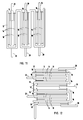
- FIG. 9 is a schematic representation of a single layer capacitor shaped or bent into a pseudo-stacked film arrangement.
- FIG. 10 is a schematic illustration of a double layer capacitor bent or shaped into a pseudo-stacked film arrangement.
- FIG. 11 is a schematic illustration of an alternative embodiment of a single layer capacitor that has been bent or shaped into a pseudo-stacked film arrangement.
- FIG. 12 is a schematic illustration of an alternative embodiment of a double layer capacitor that has been bent or shaped into a pseudo-stacked film arrangement.
- the invention utilizes a novel combination of conventional fabrication techniques employed in the fabrication of integrated circuit devices and/or other nanoscopically scaled devices, such as oxidation, metalization, polishing and patterning to provide a ceramic short-resistant capacitor that is bendable and/or shapeable to provide multiple layer capacitors that are extremely compact and amenable to desirable geometries.
- the capacitance i.e., the ability to store a charge or electrical energy
- the distance between the electrodes is proportional to the dielectric constant of the dielectric material between the electrodes and the area of overlap between the electrodes.
- Ceramic dielectrics particularly ferroelectric materials, have a dielectric constant that is typically several orders of magnitude greater than the dielectric constant for polymeric materials or air.
- the short-resistant capacitors of the invention employ very thin ceramic dielectric materials, and, therefore, have a very high capacitance per unit area.
- the capacitors of the invention are not subject to catastrophic failure, but instead exhibit what has been termed “graceful failure,” wherein there is a gradual loss of capacitance over time. Because of the high capacity and graceful or benign failure characteristics of the capacitors, they are excellent candidates for use in various applications requiring a high energy density and high reliability, such as for space hardware, battlefield equipment, hybrid vehicles, and various other industrial and communications applications.
- the capacitors of the invention have the further advantage of being shapeable or bendable, even around a relatively tight radius of curvature, thereby permitting overlapping relationships (i.e., multiple layer capacitors) that do not require leads between layers. This permits the capacitors of the invention to be shaped into any of various compact configurations more easily and at a substantially reduced cost.
- the term “shapeable” refers to a capacitor in which the electrode layers and dielectric layer between the electrode layers are sufficiently thin and malleable to allow bending of the capacitor by 180 degrees around a radius of curvature that is about 2 millimeters or less, without failure of the capacitor.
- Known short-resistant capacitors comprising a ceramic dielectric material disposed between electrode layers have required a relatively thick base electrode layer upon which the ceramic layer is deposited.
- the relatively thick base electrode layer (typically on the order of about 0.5 millimeters or 500 micrometers) rendered the completed capacitor substantially unshapeable or unbendable.
- the relatively thick base electrode was required to permit handling and mounting of the base electrode during a polishing operation.
- Polishing was necessary in order to provide a surface roughness in the range of from about 3 to about 5 nanometers (root means square over a one micrometer square area).
- a smooth surface is necessary to allow depositing of a uniformly thin ceramic layer that provides the desired high capacitance in combination with a benign failure mode.
- short-resistant refers to a capacitor that exhibits a benign failure mode, also known as graceful failure, in which a multitude of discrete failure events result in a gradual loss of capacitance.
- the number of discrete failure events that must occur before an appreciable loss of capacitance is experienced may be on the order of hundreds or even thousands of events.
- each event is a localized event (on the order of about 20 microns in diameter) in which localized heating causes an adjacent portion of one or both of the electrodes to become vaporized, thereby physically cleaning away electrode material from the defect site. In this mode of failure, shorts do not typically occur as a result of a defect failure.
- rigid substrate refers to a substrate onto which a very thin metal film may be deposited and which exhibits sufficient rigidity to facilitate processing of the thin metal layer deposited on the substrate to the desired surface roughness of 3 to 5 nanometers (root means square over a one micrometer square area).
- Suitable rigid substrates that act as carriers during assembly of the shapeable, short-resistant capacitors of the invention include silicon, quartz and ceramic substrates. Other rigid substrate materials may be possible.
- the thickness of the rigid substrate is not critical, and need only be sufficiently thick to provide a rigidity necessary for subsequent processing, which rigidity would otherwise be provided by a thicker base electrode. There is not any upper limit on the thickness of the rigid substrate.
- Suitable thicknesses for the rigid substrate, when it is silicon, quartz or ceramic, can include thicknesses ranging from hundreds of micrometers to several millimeters.
- the rigid substrate 10 can be subjected to a surface oxidation treatment to form an adhesion promoting layer 11. This should not be necessary for a quartz substrate, but may be desirable for a silicon substrate.
- layer 11 can also act as an electrical insulator, electrically isolating the subsequently deposited metal layer from the bulk or major portion of the substrate. Processes for depositing an oxide layer 11 or forming an oxide layer on a substrate are well known in the art, and do not, of themselves, constitute a novel feature of the invention.
- a silicon oxide layer may be formed on a silicon substrate by contacting the substrate with ozone and tetraethylorthosilicate (TEOS) gases and reacting ozone and TEOS in contact with the substrate to deposit silicon oxide onto the substrate.
- TEOS tetraethylorthosilicate
- adhesion promoting layer 11 may be a degradable material or a material that is weakly bonded to the metal layer 12 and/or substrate 10, such as an oxide layer grown on substrate 10, facilitating easy release and separation of first metal layer 12 from substrate 10.
- Assembly of a shapeable, short-resistant capacitor in accordance with the invention may begin by providing a substrate 10 ( FIGS. 1A and 1B ), a first metal layer 12 ( FIGs. 3A and 3B ) on the substrate or on an oxide layer 11 formed at the surface of the substrate ( FIGs. 2A and 2B ).
- This first metal layer 12 may be comprised of generally any relatively inert electrically conductive metal that can be deposited on the rigid substrate or on an oxide layer formed at the surface of the rigid substrate.
- suitable metals for the first metal layer include, but are not limited to, nickel, aluminum, copper, zinc, silver, gold, platinum, titatium, chrome or tungsten. Multiple layers may be required to promote adhesion. However, other metals may be used.
- the first metal layer 12 can be deposited on the rigid substrate 10 (or on an oxide layer formed at the surface of the rigid substrate) by any technique which provides a layer of substantially uniform thickness. Examples of suitable metal deposition techniques include, but are not limited to, sputtering, thermal evaporation, electron beam evaporation, physical vapour deposition, chemical vapour deposition, etc. Because the rigid substrate 10 provides the necessary strength and rigidity needed for subsequent processing, the first metal layer 12 need not be sufficiently thick to impart the required rigidity, but may instead be extremely thin as compared with the base layer of a conventional short-resistant capacitor. Desirably, the first metal layer 12 is sufficiently thin to allow bending and shaping and thick enough to carry the current required as previously described.
- the first metal layer 12 has a thickness less than 500 micrometers, more desirably less than 100 micrometers, and even more desirably less than 10 micrometers, with thicknesses on the order of one micrometer or even 0.1 micrometer providing desirable results.
- While deposition techniques may provide a sufficiently smooth surface that meets the criteria for a surface roughness of less than 5 nanometers (root means square over a one micrometer square area), the surface of the first metal layer 12 may undergo a conventional polishing process to achieve the desired surface roughness of less than 5 nanometers (root means square over a one micrometer square area).
- a ceramic layer 14 ( FIGs. 5A and 5B ), such as a lead lanthanum zirconium titanate (PLZT) ceramic. Also, combinations of different ceramic materials may be used. Additionally, rather than directly depositing a ceramic such as PLZT on the first metal layer 12, a buffer layer 13 may be first applied to promote adhesion and prevent diffusion between the first metal layer 12 and the PLZT or other ceramic layer 14 ( FIGs. 4A and 4B ). Use of a buffer layer 13 prevents delamination and/or oxidation of first metal layer 12, and may perform a planarizing function.
- PLZT lead lanthanum zirconium titanate
- a suitable buffer layer is a lanthanum nickel oxide (LNO) film, which may be applied to a thickness of, for example, from about 0.2 to about 0.3 micrometers.
- LNO lanthanum nickel oxide
- Another example of a suitable buffer layer that promotes adhesion between the ceramic layer 14 and the first metal layer 12 is an organic solderability preservative (OSP) coating.
- OSP organic solderability preservative
- Buffer layer 13 is optional depending on the previous metal layer(s). Buffer layer 13 requires a heat cycle up to 700 C to pyrolyze.
- a suitable thickness for the ceramic layer 14 (e.g., PLZT layer) is from about 0.5 to about 3 micrometers depending on breakdown voltage requirements. This provides a suitable and desirable combination of flexibility, high capacitance, and a benign failure mode.
- Ceramic layer 14 may require a heat cycle up to about 700 C to anneal.
- additional electrically insulative material 16 FIGs. 6A and 6B , can be applied to facilitate attachment of electrical leads to a subsequently applied second metal layer (electrode).
- the additional electrically insulative material 16 at the lead attachment area prevents electrical arcing across the electrodes at the lead attachment area, thereby eliminating the possibility of a defect failure in the area of the electrical lead connection.
- a failure at a lead connection area would result in a short circuit and catastrophic failure of the capacitor since the lead connection would prevent vaporization and self-clearing of electrode material at the lead connection.
- Suitable techniques for patterning an insulative oxide layer 16 or spin-on glass (SOG) layer are well known in the art and do not, by themselves, constitute the invention.
- a second metal layer 18 ( Figs. 7A and 7B ) is deposited on the ceramic layer 14 and over any patterned insulative material 16 deposited on the ceramic layer 14 to facilitate connection of electrical leads ( FIGs. 4A and 4B ).
- the first 12 and second 16 metal layers separated by the ceramic layer 14 define a capacitor having a high capacitance per unit area.
- the second metal film 18 is preferably deposited to a thickness in the range of from about 0.01 to about 1 micrometer (i.e., about 10 nanometers to about 1,000 nanometers).
- Such extremely thin second electrode allows complete evaporation or self-clearing of a very small area of the electrode in the event of a failure, whereby the capacitance of the entire capacitor is only very slightly reduced. As a result, numerous (e.g., hundreds or thousands) of discrete failure events may occur before the capacitor is unable to perform satisfactorily.
- Deposition of the second metal layer 18 may be accomplished by any means which provides layers of uniform thicknesses, and generally includes any of the techniques that may be used for depositing the first metal layer on the substrate, including sputtering, thermal evaporation, electron beam evaporation, chemical vapour deposition, and physical vapour deposition.
- the second metal layer 18 may be comprised of generally any metal that can be deposited on the ceramic layer, which is substantially inert, highly electrically conductive, and has a sufficiently low vaporization temperature. Examples of suitable metals include aluminum, platinum, copper, zinc, silver, gold, and combinations thereof.
- a suitable second metal layer 18 may be deposited using electron beam evaporation technique to deposit aluminium to a thickness of about 0.2 to 0.3 micrometers.
- Electrical leads 20 may be attached with solder 22 as shown in FIG. 8B or any other method known in the art.
- the next step in the fabrication process involves separating the layers of the capacitor from the substrate. This can be achieved by peeling a week bond between the Si and the first metal layer. Or by backgrinding and chemically etching the Si substrate to the desired thickness.
- the completed capacitor of the invention is shapeable or bendable so that it can be configured in a pseudo-stacked film arrangement 30, such as shown in FIG. 9 .
- gaps 32 between the stacked film layers allow venting of evaporated electrode material in the event of a benign failure.
- FIG. 10 shows a double layer capacitor that is subsequently bent into a pseudo-stacked film arrangement to provide a higher energy storage capacity per unit volume than the single layer capacitor shown in FIG. 9 , while still allowing venting of evaporated electrode material in the event of benign failure.
- the gaps 32 between adjacent stacked film layers for the embodiments shown in FIGs. 9 and 10 will depend on the radius of curvature through which the capacitor can be bent. However, it is expected that suitable gaps that may be achieved will be in the range of hundreds of micrometers to about one or two millimeters.
- FIG. 11 shows another alternative embodiment, in which the ceramic layer and the second metal layer are selectively deposited on a first metal layer by limiting the ceramic dielectric material 14 and the second metal layer 18 to areas between the bends, a smaller radius of curvature may be achieved at the bends, thus providing a more compact arrangement with a higher energy capacity per unit volume.
- FIG. 12 shows a slightly more complex arrangement in which a double layer capacitor having selectively deposited ceramic layers and second metal electrode layers to further improve compactness and energy capacity per unit volume.
- This arrangement may be achieved by forming layers 12, 14 and 18 as generally described above, separating the resulting assembly from substrate 10, remounting the resulting assembly on a substrate 10 with the side of layer 12 originally deposited on a substrate 10 facing away from the substrate to receive additional dielectric layer 50 and third metal layer 52.
- FIGs. 9, 10 , 11 and 12 may be incorporated or embedded into a circuit board design to provide a circuit board with integral capacitors.
Landscapes
- Engineering & Computer Science (AREA)
- Power Engineering (AREA)
- Microelectronics & Electronic Packaging (AREA)
- Manufacturing & Machinery (AREA)
- Fixed Capacitors And Capacitor Manufacturing Machines (AREA)
Abstract
Description
- This invention relates to electrical capacitors, and more particularly to capacitors exhibiting a benign failure mode in which failure occurs gradually due to a multitude of discrete failure events rather than a single catastrophic failure event.
- Known capacitors having a high capacitance ceramic dielectric layer and exhibiting a benign failure mode have a relatively thick base electrode that limits shapeability. Specifically, the base electrode is sufficiently thick to effectively prevent bending of the capacitor to form multiple layer capacitor structures. Such multiple layer structures and other shaped arrangements may be desired to conform the shape of the capacitor to available space of a device and/or to provide a more compact capacitor structure.
- Known capacitors exhibiting a benign failure mode are prepared by polishing a metal foil electrode (typically nickel or copper foil) to a surface roughness of 3 to 5 nanometers (root mean square roughness over a one micrometer square area). Polishing is needed because the metal foils used for preparing capacitors having a high capacitance ceramic dielectric layer and exhibiting a benign failure mode cannot be manufactured without a sufficiently smooth surface. The smoother the finish the thinner the dielectric. The thinner the dielectric layer the higher the capacitance value. This surface is needed to form a uniformly thin dielectric layer between electrode layers. However, in order to facilitate handling of the foil in a polishing operation, the foil must be of a thickness that renders the completed capacitor incapable of being shaped or bent without becoming damaged. Thus, there has not been any method of providing a highly shapeable or bendable capacitor having a high capacitance ceramic dielectric layer and exhibiting a benign failure mode.
- In one aspect of the invention, there is provided an improved method of making a capacitor having a high capacitance ceramic dielectric layer and exhibiting a benign failure mode. The improved method allows thinner and more flexible capacitors of this type to be made. These thinner, more flexible capacitors can be bent and/or shaped to form multiple layer capacitor structures that can conform to a desired geometry and/or facilitate more compact capacitor structures. The method involves forming a first thin metal layer on a substrate, and if needed a buffer layer onto the metal layer to prevent diffusion and oxidation while providing planarization. The method further includes depositing a thin, ceramic dielectric layer over the buffer layer; depositing a second thin metal layer over the dielectric layer to form a capacitor exhibiting a benign failure mode; and separating the capacitor from the substrate. The substrate provides rigidity needed during processing, thereby allowing a very thin first metal layer that can become part of a capacitor that is easily bent and which exhibits a benign failure mode.
- In another aspect, the invention provides a shapeable, short-resistant capacitor that comprises a thin ceramic dielectric material disposed between metal electrode layers, wherein the dielectric layer and each of the electrode layers are sufficiently thin to allow bending and shaping of the capacitor.
- In another aspect, the invention provides a shaped film or foil capacitor exhibiting a benign failure mode and having a plurality of overlapping layers.
- These and other features, advantages and objects of the present invention will be further understood and appreciated by those skilled in the art by reference to the following specification, claims and appended drawings.
- The present invention will now be described, by way of example, with reference to the accompanying drawings, in which:
-
FIG. 1A shows a top view of a silicon substrate used as a carrier for making a short-resistant capacitor in accordance with the invention. -
FIG. 1B is an elevational cross-sectional view as seen along lines 1B ofFIG. 1A . -
FIG. 2A is a top view of the silicon substrate ofFIG. 1A after an oxide layer has been formed. -
FIG. 2B is a cross-sectional view of the silicon substrate with oxide layer ofFIG. 2A as viewed along lines 2B-2B. -
FIG. 3A is a top view of the silicon substrate with oxide layer as shown inFIG. 2A after application of a first metal layer (multiple metal layers may be desirable for adhesion and current carrying capability). -
FIG. 3B is cross-sectional view of the silicon substrate oxide layer and metal layer ofFIG. 3A as viewed along lines 3B-3B ofFIG. 3A . -
FIG. 4A is a top view of the assembled layers ofFIG. 3A after application of a buffer layer. -
FIG. 4B is a cross-sectional view of the assembled layers shown inFIG. 4A . -
FIG. 5A is a top view of the assembled arrangement ofFIG. 4A after further application of a ceramic layer. -
FIG. 5B is a cross-sectional view of the assembled layer shown inFIG. 5A . -
FIG. 6A is a top view of the assembly ofFIG. 5A after application of a patterned oxide layer. -
FIG. 6B is a cross-sectional view of the assembly shown inFIG. 6A . -
FIG.7A is a top view of the assembly shown inFIG. 6A after application of a second electrode layer. -
FIG. 7B is a cross-sectional view of the assembly shown inFIG. 7A . -
FIG. 8A is a top view of the assembly shown inFIG. 7A after attachment of an electrical lead. -
FIG. 8B is a cross-sectional view of the assembly shown inFIG. 8A . -
FIG. 9 is a schematic representation of a single layer capacitor shaped or bent into a pseudo-stacked film arrangement. -
FIG. 10 is a schematic illustration of a double layer capacitor bent or shaped into a pseudo-stacked film arrangement. -
FIG. 11 is a schematic illustration of an alternative embodiment of a single layer capacitor that has been bent or shaped into a pseudo-stacked film arrangement. -
FIG. 12 is a schematic illustration of an alternative embodiment of a double layer capacitor that has been bent or shaped into a pseudo-stacked film arrangement. - The invention utilizes a novel combination of conventional fabrication techniques employed in the fabrication of integrated circuit devices and/or other nanoscopically scaled devices, such as oxidation, metalization, polishing and patterning to provide a ceramic short-resistant capacitor that is bendable and/or shapeable to provide multiple layer capacitors that are extremely compact and amenable to desirable geometries. For any given voltage potential across the electrodes of a capacitor, the capacitance (i.e., the ability to store a charge or electrical energy) is proportional to the dielectric constant of the dielectric material between the electrodes and the area of overlap between the electrodes, and inversely proportional to the distance between the electrodes.
- Ceramic dielectrics, particularly ferroelectric materials, have a dielectric constant that is typically several orders of magnitude greater than the dielectric constant for polymeric materials or air. The short-resistant capacitors of the invention employ very thin ceramic dielectric materials, and, therefore, have a very high capacitance per unit area. In addition, because at least one of the electrodes is extremely thin, the capacitors of the invention are not subject to catastrophic failure, but instead exhibit what has been termed "graceful failure," wherein there is a gradual loss of capacitance over time. Because of the high capacity and graceful or benign failure characteristics of the capacitors, they are excellent candidates for use in various applications requiring a high energy density and high reliability, such as for space hardware, battlefield equipment, hybrid vehicles, and various other industrial and communications applications. However, in addition to the foregoing attributes, the capacitors of the invention have the further advantage of being shapeable or bendable, even around a relatively tight radius of curvature, thereby permitting overlapping relationships (i.e., multiple layer capacitors) that do not require leads between layers. This permits the capacitors of the invention to be shaped into any of various compact configurations more easily and at a substantially reduced cost.
- As used herein, the term "shapeable" refers to a capacitor in which the electrode layers and dielectric layer between the electrode layers are sufficiently thin and malleable to allow bending of the capacitor by 180 degrees around a radius of curvature that is about 2 millimeters or less, without failure of the capacitor. Known short-resistant capacitors comprising a ceramic dielectric material disposed between electrode layers have required a relatively thick base electrode layer upon which the ceramic layer is deposited. The relatively thick base electrode layer (typically on the order of about 0.5 millimeters or 500 micrometers) rendered the completed capacitor substantially unshapeable or unbendable. The relatively thick base electrode was required to permit handling and mounting of the base electrode during a polishing operation. Polishing was necessary in order to provide a surface roughness in the range of from about 3 to about 5 nanometers (root means square over a one micrometer square area). A smooth surface is necessary to allow depositing of a uniformly thin ceramic layer that provides the desired high capacitance in combination with a benign failure mode.
- The term "short-resistant" refers to a capacitor that exhibits a benign failure mode, also known as graceful failure, in which a multitude of discrete failure events result in a gradual loss of capacitance. In many cases, the number of discrete failure events that must occur before an appreciable loss of capacitance is experienced may be on the order of hundreds or even thousands of events. In such case, each event is a localized event (on the order of about 20 microns in diameter) in which localized heating causes an adjacent portion of one or both of the electrodes to become vaporized, thereby physically cleaning away electrode material from the defect site. In this mode of failure, shorts do not typically occur as a result of a defect failure. Rather, there is a gradual loss of capacitance and failure is delayed until a predetermined or defined leakage current or dielectric loss is reached. A known ceramic capacitor exhibiting graceful failure by self-clearing is described in
U.S. Patent No. 7,099,141 , which is hereby incorporated by reference. - The term "rigid substrate" refers to a substrate onto which a very thin metal film may be deposited and which exhibits sufficient rigidity to facilitate processing of the thin metal layer deposited on the substrate to the desired surface roughness of 3 to 5 nanometers (root means square over a one micrometer square area).
- Suitable rigid substrates that act as carriers during assembly of the shapeable, short-resistant capacitors of the invention include silicon, quartz and ceramic substrates. Other rigid substrate materials may be possible. The thickness of the rigid substrate is not critical, and need only be sufficiently thick to provide a rigidity necessary for subsequent processing, which rigidity would otherwise be provided by a thicker base electrode. There is not any upper limit on the thickness of the rigid substrate. Suitable thicknesses for the rigid substrate, when it is silicon, quartz or ceramic, can include thicknesses ranging from hundreds of micrometers to several millimeters.
- In order to promote adhesion of a subsequently deposited metal layer, the
rigid substrate 10 can be subjected to a surface oxidation treatment to form anadhesion promoting layer 11. This should not be necessary for a quartz substrate, but may be desirable for a silicon substrate. In addition to promoting adhesion of afirst metal layer 12 to therigid substrate 10,layer 11 can also act as an electrical insulator, electrically isolating the subsequently deposited metal layer from the bulk or major portion of the substrate. Processes for depositing anoxide layer 11 or forming an oxide layer on a substrate are well known in the art, and do not, of themselves, constitute a novel feature of the invention. For example, a silicon oxide layer may be formed on a silicon substrate by contacting the substrate with ozone and tetraethylorthosilicate (TEOS) gases and reacting ozone and TEOS in contact with the substrate to deposit silicon oxide onto the substrate. - As will be subsequently discussed in greater detail,
adhesion promoting layer 11 may be a degradable material or a material that is weakly bonded to themetal layer 12 and/orsubstrate 10, such as an oxide layer grown onsubstrate 10, facilitating easy release and separation offirst metal layer 12 fromsubstrate 10. - Assembly of a shapeable, short-resistant capacitor in accordance with the invention may begin by providing a substrate 10 (
FIGS. 1A and 1B ), a first metal layer 12 (FIGs. 3A and 3B ) on the substrate or on anoxide layer 11 formed at the surface of the substrate (FIGs. 2A and 2B ). Thisfirst metal layer 12 may be comprised of generally any relatively inert electrically conductive metal that can be deposited on the rigid substrate or on an oxide layer formed at the surface of the rigid substrate. Examples of suitable metals for the first metal layer include, but are not limited to, nickel, aluminum, copper, zinc, silver, gold, platinum, titatium, chrome or tungsten. Multiple layers may be required to promote adhesion. However, other metals may be used. Thefirst metal layer 12 can be deposited on the rigid substrate 10 (or on an oxide layer formed at the surface of the rigid substrate) by any technique which provides a layer of substantially uniform thickness. Examples of suitable metal deposition techniques include, but are not limited to, sputtering, thermal evaporation, electron beam evaporation, physical vapour deposition, chemical vapour deposition, etc. Because therigid substrate 10 provides the necessary strength and rigidity needed for subsequent processing, thefirst metal layer 12 need not be sufficiently thick to impart the required rigidity, but may instead be extremely thin as compared with the base layer of a conventional short-resistant capacitor. Desirably, thefirst metal layer 12 is sufficiently thin to allow bending and shaping and thick enough to carry the current required as previously described. Desirably, thefirst metal layer 12 has a thickness less than 500 micrometers, more desirably less than 100 micrometers, and even more desirably less than 10 micrometers, with thicknesses on the order of one micrometer or even 0.1 micrometer providing desirable results. - While deposition techniques may provide a sufficiently smooth surface that meets the criteria for a surface roughness of less than 5 nanometers (root means square over a one micrometer square area), the surface of the
first metal layer 12 may undergo a conventional polishing process to achieve the desired surface roughness of less than 5 nanometers (root means square over a one micrometer square area). - Deposited on the
first metal layer 12 is a ceramic layer 14 (FIGs. 5A and 5B ), such as a lead lanthanum zirconium titanate (PLZT) ceramic. Also, combinations of different ceramic materials may be used. Additionally, rather than directly depositing a ceramic such as PLZT on thefirst metal layer 12, abuffer layer 13 may be first applied to promote adhesion and prevent diffusion between thefirst metal layer 12 and the PLZT or other ceramic layer 14 (FIGs. 4A and 4B ). Use of abuffer layer 13 prevents delamination and/or oxidation offirst metal layer 12, and may perform a planarizing function. An example of a suitable buffer layer is a lanthanum nickel oxide (LNO) film, which may be applied to a thickness of, for example, from about 0.2 to about 0.3 micrometers. Another example of a suitable buffer layer that promotes adhesion between theceramic layer 14 and thefirst metal layer 12 is an organic solderability preservative (OSP) coating.Buffer layer 13 is optional depending on the previous metal layer(s).Buffer layer 13 requires a heat cycle up to 700 C to pyrolyze. A suitable thickness for the ceramic layer 14 (e.g., PLZT layer) is from about 0.5 to about 3 micrometers depending on breakdown voltage requirements. This provides a suitable and desirable combination of flexibility, high capacitance, and a benign failure mode. However, slightly thinner and thicker ceramic layers can also provide adequate results. For example, thicknesses in the range of from about 0.1 to about 4 micrometers are expected to provide desirable results.Ceramic layer 14 may require a heat cycle up to about 700 C to anneal. On selected areas of the surface of theceramic layer 14, additional electrically insulative material 16 (FIGs. 6A and 6B ), can be applied to facilitate attachment of electrical leads to a subsequently applied second metal layer (electrode). By providing additionalelectrical insulation 16 at those areas of the capacitor where electrical leads are to be attached, it becomes possible to connect electrical leads to the completed capacitor without compromising the benign failure mode characteristic and without compromising short resistance. The additional electricallyinsulative material 16 at the lead attachment area prevents electrical arcing across the electrodes at the lead attachment area, thereby eliminating the possibility of a defect failure in the area of the electrical lead connection. A failure at a lead connection area would result in a short circuit and catastrophic failure of the capacitor since the lead connection would prevent vaporization and self-clearing of electrode material at the lead connection. Suitable techniques for patterning aninsulative oxide layer 16 or spin-on glass (SOG) layer are well known in the art and do not, by themselves, constitute the invention. - A second metal layer 18 (
Figs. 7A and 7B ) is deposited on theceramic layer 14 and over anypatterned insulative material 16 deposited on theceramic layer 14 to facilitate connection of electrical leads (FIGs. 4A and 4B ). The first 12 and second 16 metal layers separated by theceramic layer 14 define a capacitor having a high capacitance per unit area. Thesecond metal film 18 is preferably deposited to a thickness in the range of from about 0.01 to about 1 micrometer (i.e., about 10 nanometers to about 1,000 nanometers). Such extremely thin second electrode allows complete evaporation or self-clearing of a very small area of the electrode in the event of a failure, whereby the capacitance of the entire capacitor is only very slightly reduced. As a result, numerous (e.g., hundreds or thousands) of discrete failure events may occur before the capacitor is unable to perform satisfactorily. - Deposition of the
second metal layer 18 may be accomplished by any means which provides layers of uniform thicknesses, and generally includes any of the techniques that may be used for depositing the first metal layer on the substrate, including sputtering, thermal evaporation, electron beam evaporation, chemical vapour deposition, and physical vapour deposition. Thesecond metal layer 18 may be comprised of generally any metal that can be deposited on the ceramic layer, which is substantially inert, highly electrically conductive, and has a sufficiently low vaporization temperature. Examples of suitable metals include aluminum, platinum, copper, zinc, silver, gold, and combinations thereof. For example, a suitablesecond metal layer 18 may be deposited using electron beam evaporation technique to deposit aluminium to a thickness of about 0.2 to 0.3 micrometers. - Electrical leads 20 may be attached with
solder 22 as shown inFIG. 8B or any other method known in the art. - Following assembly of the capacitor layers as described above, the next step in the fabrication process involves separating the layers of the capacitor from the substrate. This can be achieved by peeling a week bond between the Si and the first metal layer. Or by backgrinding and chemically etching the Si substrate to the desired thickness.
- The completed capacitor of the invention is shapeable or bendable so that it can be configured in a
pseudo-stacked film arrangement 30, such as shown inFIG. 9 . In this arrangement,gaps 32 between the stacked film layers allow venting of evaporated electrode material in the event of a benign failure. -
FIG. 10 shows a double layer capacitor that is subsequently bent into a pseudo-stacked film arrangement to provide a higher energy storage capacity per unit volume than the single layer capacitor shown inFIG. 9 , while still allowing venting of evaporated electrode material in the event of benign failure. Thegaps 32 between adjacent stacked film layers for the embodiments shown inFIGs. 9 and 10 will depend on the radius of curvature through which the capacitor can be bent. However, it is expected that suitable gaps that may be achieved will be in the range of hundreds of micrometers to about one or two millimeters. After the capacitor layers 12, 14 and 18 have been prepared as described above, similar techniques may be employed to add asecond dielectric layer 40 and athird metal layer 42 before separating the assembly fromsubstrate 10. -
FIG. 11 shows another alternative embodiment, in which the ceramic layer and the second metal layer are selectively deposited on a first metal layer by limiting the ceramicdielectric material 14 and thesecond metal layer 18 to areas between the bends, a smaller radius of curvature may be achieved at the bends, thus providing a more compact arrangement with a higher energy capacity per unit volume. -
FIG. 12 shows a slightly more complex arrangement in which a double layer capacitor having selectively deposited ceramic layers and second metal electrode layers to further improve compactness and energy capacity per unit volume. This arrangement may be achieved by forminglayers substrate 10, remounting the resulting assembly on asubstrate 10 with the side oflayer 12 originally deposited on asubstrate 10 facing away from the substrate to receive additionaldielectric layer 50 andthird metal layer 52. - Other possible configurations include spiral wound capacitors.
- The various embodiments shown in
FIGs. 9, 10 ,11 and 12 may be incorporated or embedded into a circuit board design to provide a circuit board with integral capacitors. - It will be understood by those who practice the invention and those skilled in the art, that various modifications and improvements may be made to the invention without departing from the spirit of the disclosed concept. The scope of protection afforded is to be determined by the claims and by the breadth of interpretation allowed by law.
Claims (17)
- A method of making a shapeable, short-resistant capacitor (30), comprising:providing a rigid substrate (10);
optionally depositing a buffer layer (13) to promote adhesion, prevent diffusion, prevent oxidation, and/or provide planarization;
optionally applying a release layer;
depositing a first metal layer (12) on the substrate (10), or on the optional release layer when the release layer is present and the optional buffer layer (13) is not present, or on the buffer layer (13) when it is present;
depositing a ceramic layer (14) on the first metal layer (12);
depositing a second metal layer (18) on the ceramic layer (14) to form a short-resistant capacitor (30) comprising the ceramic layer (14) disposed between the first metal layer (12) and the second metal layer (18); and
separating the short-resistant capacitor (30) from the substrate (10). - A method of claim 1, wherein the substrate (10) is comprised of quartz.
- A method of claim 1 or claim 2, wherein the buffer layer (13) is a silicon oxide.
- A method of any one of claims 1 to 3, wherein the release layer is a material weakly bonded to the metal layer (12) and/or substrate (10).
- A method of any one of claims 1 to 4, wherein the first metal layer (12) is comprised of a material selected from the group consisting of nickel, aluminum, copper, zinc, silver, gold , platinum, titatium, chrome and tungsten.
- A method of claim 5, wherein the first metal layer (12) is deposited at a thickness of from about 0.1 micrometers to 500 micrometers.
- A method of any one of claims 1 to 6, wherein the ceramic material (14) is lead lanthanum zirconium titanate (PLZT).
- A method of any one of claims 1 to 7, further comprising a buffer layer (13) between the first metal layer (12) and the ceramic layer (14) to prevent diffusion and oxidation while providing planarization.
- A method of claim 8, wherein the buffer layer (13) is a lanthanum nickel oxide film.
- A method of claim 9, wherein the lanthanum nickel oxide film has a thickness of from 0.2 to 0.3 micrometers.
- A method of any one of claims 1 to 10, wherein the ceramic layer (14) is deposited to a thickness of from 0.1 to 4 micrometers.
- A method of any one of claims 1 to 11, further comprising depositing additional electrically insulative material (16) on selected areas of the ceramic layer (14) before depositing the second metal layer (18) to facilitate attachment of electrical leads (20).
- A method of claim 12, wherein the additional electrically insulative material is an insulative oxide.
- A method of any one of claims 1 to 13, wherein the second metal layer (18) is deposited to a thickness of from 0.01 to 0.1 micrometers.
- A method of claim 14, wherein the second metal layer (18) is comprised of a material selected from aluminium, platinum, copper, zinc, silver, gold and combinations of these metals.
- A method of any one of claims 1 to 15, further comprising bending the resulting short-resistant capacitor (30) into a pseudo-stacked film arrangement with gaps (32) between the stacked film layers that allow venting of evaporated electrode material in the event of a benign failure.
- A method of any one of claims 1 to 16, further comprising depositing a second ceramic layer on the second metal layer and depositing a third metal layer on the second ceramic layer before separating a resulting double layer capacitor from the substrate.
Applications Claiming Priority (1)
| Application Number | Priority Date | Filing Date | Title |
|---|---|---|---|
| US12/498,025 US8407871B2 (en) | 2009-07-06 | 2009-07-06 | Method of manufacturing a shapeable short-resistant capacitor |
Publications (2)
| Publication Number | Publication Date |
|---|---|
| EP2273517A1 true EP2273517A1 (en) | 2011-01-12 |
| EP2273517B1 EP2273517B1 (en) | 2016-10-19 |
Family
ID=42752899
Family Applications (1)
| Application Number | Title | Priority Date | Filing Date |
|---|---|---|---|
| EP10167297.0A Active EP2273517B1 (en) | 2009-07-06 | 2010-06-25 | Shapeable short-resistant capacitor |
Country Status (2)
| Country | Link |
|---|---|
| US (2) | US8407871B2 (en) |
| EP (1) | EP2273517B1 (en) |
Cited By (1)
| Publication number | Priority date | Publication date | Assignee | Title |
|---|---|---|---|---|
| EP3239999A1 (en) * | 2016-04-18 | 2017-11-01 | Delphi Technologies, Inc. | Ceramic-wound-capacitor with lead lanthanum zirconium titanate dielectric (plzt) |
Families Citing this family (7)
| Publication number | Priority date | Publication date | Assignee | Title |
|---|---|---|---|---|
| US9025311B1 (en) | 2012-04-25 | 2015-05-05 | Kemet Electronics Corporation | Very large ceramic capacitor with mechanical shock resistance |
| US9646766B2 (en) | 2012-06-14 | 2017-05-09 | Uchicago Argonne, Llc | Method of making dielectric capacitors with increased dielectric breakdown strength |
| WO2014203633A1 (en) * | 2013-06-17 | 2014-12-24 | 株式会社村田製作所 | Flexible cable and electronic apparatus |
| KR102255798B1 (en) * | 2014-08-04 | 2021-05-26 | (주)포인트엔지니어링 | Multi-layerd Aluminium oxide capacitor |
| EP3313131B1 (en) | 2015-07-27 | 2020-04-29 | Huawei Technologies Co., Ltd. | Information transmission method and related apparatus |
| US11284840B1 (en) | 2016-08-26 | 2022-03-29 | W. L. Gore & Associates, Inc. | Calibrating passive LC sensor |
| US10429252B1 (en) * | 2016-08-26 | 2019-10-01 | W. L. Gore & Associates, Inc. | Flexible capacitive pressure sensor |
Citations (5)
| Publication number | Priority date | Publication date | Assignee | Title |
|---|---|---|---|---|
| GB1030820A (en) * | 1963-11-13 | 1966-05-25 | Siemens Ag | Improvements in or relating to the manufacture of capacitor strip assemblies |
| US5032461A (en) * | 1983-12-19 | 1991-07-16 | Spectrum Control, Inc. | Method of making a multi-layered article |
| US7099141B1 (en) | 2005-06-06 | 2006-08-29 | The United States Of America As Represented By The United States Department Of Energy | Ceramic capacitor exhibiting graceful failure by self-clearing, method for fabricating self-clearing capacitor |
| US20070202257A1 (en) * | 2006-02-28 | 2007-08-30 | Tdk Corporation | Production method of multilayer ceramic electronic device |
| WO2010028492A1 (en) * | 2008-09-12 | 2010-03-18 | David Allan Kelly | Capacitor method of fabrication |
Family Cites Families (10)
| Publication number | Priority date | Publication date | Assignee | Title |
|---|---|---|---|---|
| US3894872A (en) * | 1974-07-17 | 1975-07-15 | Rca Corp | Technique for fabricating high Q MIM capacitors |
| DE2513858C3 (en) * | 1975-03-27 | 1981-08-06 | Siemens AG, 1000 Berlin und 8000 München | Process for the production of a tantalum thin film capacitor |
| US4146914A (en) * | 1977-07-12 | 1979-03-27 | Illinois Tool Works Inc. | Pleated metallized film capacitor with staggered edges |
| US4234338A (en) * | 1978-12-28 | 1980-11-18 | The United States Of America As Represented By The United States Department Of Energy | Thermal shock resistance ceramic insulator |
| DE69931334T2 (en) * | 1998-12-22 | 2007-02-01 | Matsushita Electric Industrial Co., Ltd., Kadoma | Flexible thin-film capacitor and manufacturing process |
| US6414377B1 (en) * | 1999-08-10 | 2002-07-02 | International Business Machines Corporation | Low k dielectric materials with inherent copper ion migration barrier |
| JP3861669B2 (en) * | 2001-11-22 | 2006-12-20 | ソニー株式会社 | Manufacturing method of multichip circuit module |
| KR100471163B1 (en) * | 2002-03-14 | 2005-03-09 | 삼성전자주식회사 | Methods of forming a semiconductor device having capacitors |
| JP2004111588A (en) * | 2002-09-18 | 2004-04-08 | Toshiba Corp | Capacitor and manufacturing method thereof |
| US7367119B2 (en) * | 2005-06-24 | 2008-05-06 | Nanochip, Inc. | Method for forming a reinforced tip for a probe storage device |
-
2009
- 2009-07-06 US US12/498,025 patent/US8407871B2/en active Active
-
2010
- 2010-06-25 EP EP10167297.0A patent/EP2273517B1/en active Active
-
2013
- 2013-01-29 US US13/752,441 patent/US9153380B2/en active Active
Patent Citations (5)
| Publication number | Priority date | Publication date | Assignee | Title |
|---|---|---|---|---|
| GB1030820A (en) * | 1963-11-13 | 1966-05-25 | Siemens Ag | Improvements in or relating to the manufacture of capacitor strip assemblies |
| US5032461A (en) * | 1983-12-19 | 1991-07-16 | Spectrum Control, Inc. | Method of making a multi-layered article |
| US7099141B1 (en) | 2005-06-06 | 2006-08-29 | The United States Of America As Represented By The United States Department Of Energy | Ceramic capacitor exhibiting graceful failure by self-clearing, method for fabricating self-clearing capacitor |
| US20070202257A1 (en) * | 2006-02-28 | 2007-08-30 | Tdk Corporation | Production method of multilayer ceramic electronic device |
| WO2010028492A1 (en) * | 2008-09-12 | 2010-03-18 | David Allan Kelly | Capacitor method of fabrication |
Cited By (2)
| Publication number | Priority date | Publication date | Assignee | Title |
|---|---|---|---|---|
| EP3239999A1 (en) * | 2016-04-18 | 2017-11-01 | Delphi Technologies, Inc. | Ceramic-wound-capacitor with lead lanthanum zirconium titanate dielectric (plzt) |
| US10163572B2 (en) | 2016-04-18 | 2018-12-25 | Delphi Technologies Ip Limited | Ceramic-wound-capacitor with lead lanthanum zirconium titanate dielectric |
Also Published As
| Publication number | Publication date |
|---|---|
| US20110002081A1 (en) | 2011-01-06 |
| US9153380B2 (en) | 2015-10-06 |
| US20130148255A1 (en) | 2013-06-13 |
| EP2273517B1 (en) | 2016-10-19 |
| US8407871B2 (en) | 2013-04-02 |
Similar Documents
| Publication | Publication Date | Title |
|---|---|---|
| US9153380B2 (en) | Shapeable short circuit resistant capacitor | |
| US10490355B2 (en) | Thin film capacitor and manufacturing method thereof | |
| JP2020188144A (en) | Electronic component packaging structure and manufacturing method therefor | |
| US9908817B2 (en) | Multilayer capacitors, method for making multilayer capacitors | |
| US20170287642A1 (en) | Multi-layer ceramic electronic component and method of producing the same | |
| US10395842B2 (en) | Thin film capacitor and manufacturing method thereof | |
| JP2006521224A (en) | Manufacturing method of laminated structure | |
| JP7738278B2 (en) | Capacitor, electric circuit, circuit board, electronic device, and power storage device | |
| EP2254132B1 (en) | Contact for ceramic capacitor with self-clearing feature | |
| US11728097B2 (en) | Multilayer electronic component | |
| US20180350523A1 (en) | Roll-up capacitor and method for producing the same | |
| KR101901708B1 (en) | Multilayer ceramic capacitor and method for fabricating the same | |
| US12462977B2 (en) | Multilayer ceramic electronic component including via conductors not exposed to principal surfaces | |
| JP2021136323A (en) | Multilayer ceramic electronic component | |
| US10679793B2 (en) | Roll-up type capacitor and process for producing the same | |
| US11735365B2 (en) | Multilayer capacitor, board for mounting the same, and method of manufacturing the same | |
| US10950389B2 (en) | Thin-film capacitor | |
| US10319526B2 (en) | Thin-film capacitor | |
| US12518930B2 (en) | Multilayer ceramic capacitor including SiO2 film on surfaces thereof | |
| US20240249885A1 (en) | Multilayer ceramic electronic component | |
| US20140118881A1 (en) | Capacitor and method of manufacturing the same | |
| US20250218683A1 (en) | Multilayer electronic component | |
| JP2007242880A (en) | Film deposition method | |
| CN119786261A (en) | Multilayer electronic components | |
| CN119943578A (en) | Multilayer Ceramic Capacitors |
Legal Events
| Date | Code | Title | Description |
|---|---|---|---|
| PUAI | Public reference made under article 153(3) epc to a published international application that has entered the european phase |
Free format text: ORIGINAL CODE: 0009012 |
|
| AK | Designated contracting states |
Kind code of ref document: A1 Designated state(s): AL AT BE BG CH CY CZ DE DK EE ES FI FR GB GR HR HU IE IS IT LI LT LU LV MC MK MT NL NO PL PT RO SE SI SK SM TR |
|
| AX | Request for extension of the european patent |
Extension state: BA ME RS |
|
| 17P | Request for examination filed |
Effective date: 20110712 |
|
| GRAP | Despatch of communication of intention to grant a patent |
Free format text: ORIGINAL CODE: EPIDOSNIGR1 |
|
| INTG | Intention to grant announced |
Effective date: 20160506 |
|
| GRAS | Grant fee paid |
Free format text: ORIGINAL CODE: EPIDOSNIGR3 |
|
| GRAA | (expected) grant |
Free format text: ORIGINAL CODE: 0009210 |
|
| AK | Designated contracting states |
Kind code of ref document: B1 Designated state(s): AL AT BE BG CH CY CZ DE DK EE ES FI FR GB GR HR HU IE IS IT LI LT LU LV MC MK MT NL NO PL PT RO SE SI SK SM TR |
|
| REG | Reference to a national code |
Ref country code: GB Ref legal event code: FG4D |
|
| REG | Reference to a national code |
Ref country code: CH Ref legal event code: EP |
|
| REG | Reference to a national code |
Ref country code: AT Ref legal event code: REF Ref document number: 838949 Country of ref document: AT Kind code of ref document: T Effective date: 20161115 |
|
| REG | Reference to a national code |
Ref country code: IE Ref legal event code: FG4D |
|
| REG | Reference to a national code |
Ref country code: DE Ref legal event code: R096 Ref document number: 602010037269 Country of ref document: DE |
|
| REG | Reference to a national code |
Ref country code: NL Ref legal event code: MP Effective date: 20161019 |
|
| REG | Reference to a national code |
Ref country code: LT Ref legal event code: MG4D |
|
| PG25 | Lapsed in a contracting state [announced via postgrant information from national office to epo] |
Ref country code: LV Free format text: LAPSE BECAUSE OF FAILURE TO SUBMIT A TRANSLATION OF THE DESCRIPTION OR TO PAY THE FEE WITHIN THE PRESCRIBED TIME-LIMIT Effective date: 20161019 |
|
| REG | Reference to a national code |
Ref country code: AT Ref legal event code: MK05 Ref document number: 838949 Country of ref document: AT Kind code of ref document: T Effective date: 20161019 |
|
| PG25 | Lapsed in a contracting state [announced via postgrant information from national office to epo] |
Ref country code: GR Free format text: LAPSE BECAUSE OF FAILURE TO SUBMIT A TRANSLATION OF THE DESCRIPTION OR TO PAY THE FEE WITHIN THE PRESCRIBED TIME-LIMIT Effective date: 20170120 Ref country code: NO Free format text: LAPSE BECAUSE OF FAILURE TO SUBMIT A TRANSLATION OF THE DESCRIPTION OR TO PAY THE FEE WITHIN THE PRESCRIBED TIME-LIMIT Effective date: 20170119 Ref country code: SE Free format text: LAPSE BECAUSE OF FAILURE TO SUBMIT A TRANSLATION OF THE DESCRIPTION OR TO PAY THE FEE WITHIN THE PRESCRIBED TIME-LIMIT Effective date: 20161019 Ref country code: LT Free format text: LAPSE BECAUSE OF FAILURE TO SUBMIT A TRANSLATION OF THE DESCRIPTION OR TO PAY THE FEE WITHIN THE PRESCRIBED TIME-LIMIT Effective date: 20161019 |
|
| PG25 | Lapsed in a contracting state [announced via postgrant information from national office to epo] |
Ref country code: NL Free format text: LAPSE BECAUSE OF FAILURE TO SUBMIT A TRANSLATION OF THE DESCRIPTION OR TO PAY THE FEE WITHIN THE PRESCRIBED TIME-LIMIT Effective date: 20161019 Ref country code: IS Free format text: LAPSE BECAUSE OF FAILURE TO SUBMIT A TRANSLATION OF THE DESCRIPTION OR TO PAY THE FEE WITHIN THE PRESCRIBED TIME-LIMIT Effective date: 20170219 Ref country code: PT Free format text: LAPSE BECAUSE OF FAILURE TO SUBMIT A TRANSLATION OF THE DESCRIPTION OR TO PAY THE FEE WITHIN THE PRESCRIBED TIME-LIMIT Effective date: 20170220 Ref country code: ES Free format text: LAPSE BECAUSE OF FAILURE TO SUBMIT A TRANSLATION OF THE DESCRIPTION OR TO PAY THE FEE WITHIN THE PRESCRIBED TIME-LIMIT Effective date: 20161019 Ref country code: BE Free format text: LAPSE BECAUSE OF FAILURE TO SUBMIT A TRANSLATION OF THE DESCRIPTION OR TO PAY THE FEE WITHIN THE PRESCRIBED TIME-LIMIT Effective date: 20161019 Ref country code: PL Free format text: LAPSE BECAUSE OF FAILURE TO SUBMIT A TRANSLATION OF THE DESCRIPTION OR TO PAY THE FEE WITHIN THE PRESCRIBED TIME-LIMIT Effective date: 20161019 Ref country code: FI Free format text: LAPSE BECAUSE OF FAILURE TO SUBMIT A TRANSLATION OF THE DESCRIPTION OR TO PAY THE FEE WITHIN THE PRESCRIBED TIME-LIMIT Effective date: 20161019 Ref country code: AT Free format text: LAPSE BECAUSE OF FAILURE TO SUBMIT A TRANSLATION OF THE DESCRIPTION OR TO PAY THE FEE WITHIN THE PRESCRIBED TIME-LIMIT Effective date: 20161019 Ref country code: HR Free format text: LAPSE BECAUSE OF FAILURE TO SUBMIT A TRANSLATION OF THE DESCRIPTION OR TO PAY THE FEE WITHIN THE PRESCRIBED TIME-LIMIT Effective date: 20161019 |
|
| REG | Reference to a national code |
Ref country code: FR Ref legal event code: PLFP Year of fee payment: 8 |
|
| REG | Reference to a national code |
Ref country code: DE Ref legal event code: R097 Ref document number: 602010037269 Country of ref document: DE |
|
| PG25 | Lapsed in a contracting state [announced via postgrant information from national office to epo] |
Ref country code: DK Free format text: LAPSE BECAUSE OF FAILURE TO SUBMIT A TRANSLATION OF THE DESCRIPTION OR TO PAY THE FEE WITHIN THE PRESCRIBED TIME-LIMIT Effective date: 20161019 Ref country code: EE Free format text: LAPSE BECAUSE OF FAILURE TO SUBMIT A TRANSLATION OF THE DESCRIPTION OR TO PAY THE FEE WITHIN THE PRESCRIBED TIME-LIMIT Effective date: 20161019 Ref country code: CZ Free format text: LAPSE BECAUSE OF FAILURE TO SUBMIT A TRANSLATION OF THE DESCRIPTION OR TO PAY THE FEE WITHIN THE PRESCRIBED TIME-LIMIT Effective date: 20161019 Ref country code: RO Free format text: LAPSE BECAUSE OF FAILURE TO SUBMIT A TRANSLATION OF THE DESCRIPTION OR TO PAY THE FEE WITHIN THE PRESCRIBED TIME-LIMIT Effective date: 20161019 Ref country code: SK Free format text: LAPSE BECAUSE OF FAILURE TO SUBMIT A TRANSLATION OF THE DESCRIPTION OR TO PAY THE FEE WITHIN THE PRESCRIBED TIME-LIMIT Effective date: 20161019 |
|
| PLBE | No opposition filed within time limit |
Free format text: ORIGINAL CODE: 0009261 |
|
| STAA | Information on the status of an ep patent application or granted ep patent |
Free format text: STATUS: NO OPPOSITION FILED WITHIN TIME LIMIT |
|
| PG25 | Lapsed in a contracting state [announced via postgrant information from national office to epo] |
Ref country code: BG Free format text: LAPSE BECAUSE OF FAILURE TO SUBMIT A TRANSLATION OF THE DESCRIPTION OR TO PAY THE FEE WITHIN THE PRESCRIBED TIME-LIMIT Effective date: 20170119 Ref country code: IT Free format text: LAPSE BECAUSE OF FAILURE TO SUBMIT A TRANSLATION OF THE DESCRIPTION OR TO PAY THE FEE WITHIN THE PRESCRIBED TIME-LIMIT Effective date: 20161019 Ref country code: SM Free format text: LAPSE BECAUSE OF FAILURE TO SUBMIT A TRANSLATION OF THE DESCRIPTION OR TO PAY THE FEE WITHIN THE PRESCRIBED TIME-LIMIT Effective date: 20161019 |
|
| 26N | No opposition filed |
Effective date: 20170720 |
|
| PG25 | Lapsed in a contracting state [announced via postgrant information from national office to epo] |
Ref country code: SI Free format text: LAPSE BECAUSE OF FAILURE TO SUBMIT A TRANSLATION OF THE DESCRIPTION OR TO PAY THE FEE WITHIN THE PRESCRIBED TIME-LIMIT Effective date: 20161019 |
|
| PG25 | Lapsed in a contracting state [announced via postgrant information from national office to epo] |
Ref country code: MC Free format text: LAPSE BECAUSE OF FAILURE TO SUBMIT A TRANSLATION OF THE DESCRIPTION OR TO PAY THE FEE WITHIN THE PRESCRIBED TIME-LIMIT Effective date: 20161019 |
|
| REG | Reference to a national code |
Ref country code: CH Ref legal event code: PL |
|
| REG | Reference to a national code |
Ref country code: IE Ref legal event code: MM4A |
|
| PG25 | Lapsed in a contracting state [announced via postgrant information from national office to epo] |
Ref country code: LI Free format text: LAPSE BECAUSE OF NON-PAYMENT OF DUE FEES Effective date: 20170630 Ref country code: IE Free format text: LAPSE BECAUSE OF NON-PAYMENT OF DUE FEES Effective date: 20170625 Ref country code: LU Free format text: LAPSE BECAUSE OF NON-PAYMENT OF DUE FEES Effective date: 20170625 Ref country code: CH Free format text: LAPSE BECAUSE OF NON-PAYMENT OF DUE FEES Effective date: 20170630 |
|
| REG | Reference to a national code |
Ref country code: FR Ref legal event code: PLFP Year of fee payment: 9 |
|
| PG25 | Lapsed in a contracting state [announced via postgrant information from national office to epo] |
Ref country code: MT Free format text: LAPSE BECAUSE OF NON-PAYMENT OF DUE FEES Effective date: 20170625 |
|
| REG | Reference to a national code |
Ref country code: DE Ref legal event code: R081 Ref document number: 602010037269 Country of ref document: DE Owner name: DELPHI TECHNOLOGIES IP LIMITED, BB Free format text: FORMER OWNER: DELPHI TECHNOLOGIES, INC., TROY, MICH., US |
|
| REG | Reference to a national code |
Ref country code: GB Ref legal event code: 732E Free format text: REGISTERED BETWEEN 20190214 AND 20190221 |
|
| PG25 | Lapsed in a contracting state [announced via postgrant information from national office to epo] |
Ref country code: HU Free format text: LAPSE BECAUSE OF FAILURE TO SUBMIT A TRANSLATION OF THE DESCRIPTION OR TO PAY THE FEE WITHIN THE PRESCRIBED TIME-LIMIT; INVALID AB INITIO Effective date: 20100625 |
|
| PG25 | Lapsed in a contracting state [announced via postgrant information from national office to epo] |
Ref country code: CY Free format text: LAPSE BECAUSE OF NON-PAYMENT OF DUE FEES Effective date: 20161019 |
|
| PG25 | Lapsed in a contracting state [announced via postgrant information from national office to epo] |
Ref country code: MK Free format text: LAPSE BECAUSE OF FAILURE TO SUBMIT A TRANSLATION OF THE DESCRIPTION OR TO PAY THE FEE WITHIN THE PRESCRIBED TIME-LIMIT Effective date: 20161019 |
|
| PG25 | Lapsed in a contracting state [announced via postgrant information from national office to epo] |
Ref country code: TR Free format text: LAPSE BECAUSE OF FAILURE TO SUBMIT A TRANSLATION OF THE DESCRIPTION OR TO PAY THE FEE WITHIN THE PRESCRIBED TIME-LIMIT Effective date: 20161019 |
|
| PG25 | Lapsed in a contracting state [announced via postgrant information from national office to epo] |
Ref country code: AL Free format text: LAPSE BECAUSE OF FAILURE TO SUBMIT A TRANSLATION OF THE DESCRIPTION OR TO PAY THE FEE WITHIN THE PRESCRIBED TIME-LIMIT Effective date: 20161019 |
|
| P01 | Opt-out of the competence of the unified patent court (upc) registered |
Effective date: 20230327 |
|
| PGFP | Annual fee paid to national office [announced via postgrant information from national office to epo] |
Ref country code: DE Payment date: 20250509 Year of fee payment: 16 |
|
| PGFP | Annual fee paid to national office [announced via postgrant information from national office to epo] |
Ref country code: GB Payment date: 20250508 Year of fee payment: 16 |
|
| PGFP | Annual fee paid to national office [announced via postgrant information from national office to epo] |
Ref country code: FR Payment date: 20250512 Year of fee payment: 16 |