EP2271187A2 - Controlling and measuring the functions of an electronic ballast - Google Patents
Controlling and measuring the functions of an electronic ballast Download PDFInfo
- Publication number
- EP2271187A2 EP2271187A2 EP10163702A EP10163702A EP2271187A2 EP 2271187 A2 EP2271187 A2 EP 2271187A2 EP 10163702 A EP10163702 A EP 10163702A EP 10163702 A EP10163702 A EP 10163702A EP 2271187 A2 EP2271187 A2 EP 2271187A2
- Authority
- EP
- European Patent Office
- Prior art keywords
- lamp
- resistor
- electronic ballast
- current
- switching
- Prior art date
- Legal status (The legal status is an assumption and is not a legal conclusion. Google has not performed a legal analysis and makes no representation as to the accuracy of the status listed.)
- Granted
Links
- 230000005855 radiation Effects 0.000 claims abstract description 8
- 238000004519 manufacturing process Methods 0.000 claims abstract description 6
- 230000001105 regulatory effect Effects 0.000 claims abstract description 5
- 239000003990 capacitor Substances 0.000 claims description 8
- 229920006395 saturated elastomer Polymers 0.000 claims description 2
- 238000000034 method Methods 0.000 description 4
- 238000005259 measurement Methods 0.000 description 3
- 230000008569 process Effects 0.000 description 3
- XKRFYHLGVUSROY-UHFFFAOYSA-N Argon Chemical compound [Ar] XKRFYHLGVUSROY-UHFFFAOYSA-N 0.000 description 2
- 230000008901 benefit Effects 0.000 description 2
- 230000001276 controlling effect Effects 0.000 description 2
- 238000010586 diagram Methods 0.000 description 2
- QSHDDOUJBYECFT-UHFFFAOYSA-N mercury Chemical compound [Hg] QSHDDOUJBYECFT-UHFFFAOYSA-N 0.000 description 2
- 230000001960 triggered effect Effects 0.000 description 2
- 229910052786 argon Inorganic materials 0.000 description 1
- 230000008859 change Effects 0.000 description 1
- 230000000694 effects Effects 0.000 description 1
- 230000005611 electricity Effects 0.000 description 1
- 230000008030 elimination Effects 0.000 description 1
- 238000003379 elimination reaction Methods 0.000 description 1
- 238000005516 engineering process Methods 0.000 description 1
- 239000007789 gas Substances 0.000 description 1
- 238000005286 illumination Methods 0.000 description 1
- 229910052743 krypton Inorganic materials 0.000 description 1
- DNNSSWSSYDEUBZ-UHFFFAOYSA-N krypton atom Chemical compound [Kr] DNNSSWSSYDEUBZ-UHFFFAOYSA-N 0.000 description 1
- 239000000463 material Substances 0.000 description 1
- 229910052753 mercury Inorganic materials 0.000 description 1
- 230000004044 response Effects 0.000 description 1
- 230000007704 transition Effects 0.000 description 1
Images


Classifications
-
- H—ELECTRICITY
- H05—ELECTRIC TECHNIQUES NOT OTHERWISE PROVIDED FOR
- H05B—ELECTRIC HEATING; ELECTRIC LIGHT SOURCES NOT OTHERWISE PROVIDED FOR; CIRCUIT ARRANGEMENTS FOR ELECTRIC LIGHT SOURCES, IN GENERAL
- H05B41/00—Circuit arrangements or apparatus for igniting or operating discharge lamps
- H05B41/14—Circuit arrangements
- H05B41/26—Circuit arrangements in which the lamp is fed by power derived from DC by means of a converter, e.g. by high-voltage DC
- H05B41/28—Circuit arrangements in which the lamp is fed by power derived from DC by means of a converter, e.g. by high-voltage DC using static converters
- H05B41/282—Circuit arrangements in which the lamp is fed by power derived from DC by means of a converter, e.g. by high-voltage DC using static converters with semiconductor devices
- H05B41/285—Arrangements for protecting lamps or circuits against abnormal operating conditions
- H05B41/2851—Arrangements for protecting lamps or circuits against abnormal operating conditions for protecting the circuit against abnormal operating conditions
-
- H—ELECTRICITY
- H05—ELECTRIC TECHNIQUES NOT OTHERWISE PROVIDED FOR
- H05B—ELECTRIC HEATING; ELECTRIC LIGHT SOURCES NOT OTHERWISE PROVIDED FOR; CIRCUIT ARRANGEMENTS FOR ELECTRIC LIGHT SOURCES, IN GENERAL
- H05B41/00—Circuit arrangements or apparatus for igniting or operating discharge lamps
- H05B41/14—Circuit arrangements
- H05B41/26—Circuit arrangements in which the lamp is fed by power derived from DC by means of a converter, e.g. by high-voltage DC
- H05B41/28—Circuit arrangements in which the lamp is fed by power derived from DC by means of a converter, e.g. by high-voltage DC using static converters
- H05B41/295—Circuit arrangements in which the lamp is fed by power derived from DC by means of a converter, e.g. by high-voltage DC using static converters with semiconductor devices and specially adapted for lamps with preheating electrodes, e.g. for fluorescent lamps
- H05B41/298—Arrangements for protecting lamps or circuits against abnormal operating conditions
- H05B41/2981—Arrangements for protecting lamps or circuits against abnormal operating conditions for protecting the circuit against abnormal operating conditions
- H05B41/2986—Arrangements for protecting lamps or circuits against abnormal operating conditions for protecting the circuit against abnormal operating conditions against internal abnormal circuit conditions
-
- H—ELECTRICITY
- H05—ELECTRIC TECHNIQUES NOT OTHERWISE PROVIDED FOR
- H05B—ELECTRIC HEATING; ELECTRIC LIGHT SOURCES NOT OTHERWISE PROVIDED FOR; CIRCUIT ARRANGEMENTS FOR ELECTRIC LIGHT SOURCES, IN GENERAL
- H05B41/00—Circuit arrangements or apparatus for igniting or operating discharge lamps
- H05B41/14—Circuit arrangements
- H05B41/26—Circuit arrangements in which the lamp is fed by power derived from DC by means of a converter, e.g. by high-voltage DC
- H05B41/28—Circuit arrangements in which the lamp is fed by power derived from DC by means of a converter, e.g. by high-voltage DC using static converters
- H05B41/282—Circuit arrangements in which the lamp is fed by power derived from DC by means of a converter, e.g. by high-voltage DC using static converters with semiconductor devices
- H05B41/2825—Circuit arrangements in which the lamp is fed by power derived from DC by means of a converter, e.g. by high-voltage DC using static converters with semiconductor devices by means of a bridge converter in the final stage
-
- H—ELECTRICITY
- H05—ELECTRIC TECHNIQUES NOT OTHERWISE PROVIDED FOR
- H05B—ELECTRIC HEATING; ELECTRIC LIGHT SOURCES NOT OTHERWISE PROVIDED FOR; CIRCUIT ARRANGEMENTS FOR ELECTRIC LIGHT SOURCES, IN GENERAL
- H05B41/00—Circuit arrangements or apparatus for igniting or operating discharge lamps
- H05B41/14—Circuit arrangements
- H05B41/26—Circuit arrangements in which the lamp is fed by power derived from DC by means of a converter, e.g. by high-voltage DC
- H05B41/28—Circuit arrangements in which the lamp is fed by power derived from DC by means of a converter, e.g. by high-voltage DC using static converters
- H05B41/288—Circuit arrangements in which the lamp is fed by power derived from DC by means of a converter, e.g. by high-voltage DC using static converters with semiconductor devices and specially adapted for lamps without preheating electrodes, e.g. for high-intensity discharge lamps, high-pressure mercury or sodium lamps or low-pressure sodium lamps
- H05B41/292—Arrangements for protecting lamps or circuits against abnormal operating conditions
- H05B41/2921—Arrangements for protecting lamps or circuits against abnormal operating conditions for protecting the circuit against abnormal operating conditions
-
- H—ELECTRICITY
- H05—ELECTRIC TECHNIQUES NOT OTHERWISE PROVIDED FOR
- H05B—ELECTRIC HEATING; ELECTRIC LIGHT SOURCES NOT OTHERWISE PROVIDED FOR; CIRCUIT ARRANGEMENTS FOR ELECTRIC LIGHT SOURCES, IN GENERAL
- H05B41/00—Circuit arrangements or apparatus for igniting or operating discharge lamps
- H05B41/14—Circuit arrangements
- H05B41/26—Circuit arrangements in which the lamp is fed by power derived from DC by means of a converter, e.g. by high-voltage DC
- H05B41/28—Circuit arrangements in which the lamp is fed by power derived from DC by means of a converter, e.g. by high-voltage DC using static converters
- H05B41/295—Circuit arrangements in which the lamp is fed by power derived from DC by means of a converter, e.g. by high-voltage DC using static converters with semiconductor devices and specially adapted for lamps with preheating electrodes, e.g. for fluorescent lamps
- H05B41/298—Arrangements for protecting lamps or circuits against abnormal operating conditions
- H05B41/2981—Arrangements for protecting lamps or circuits against abnormal operating conditions for protecting the circuit against abnormal operating conditions
Definitions
- Tubular fluorescent lamps and HID lamps High Intensity Discharge are connected by way of electronic ballasts with a supply of electric power, receiving therefrom the energy needed thereby for illumination while being switched to the ON state.
- the fluorescent tube of fluorescent lamps and HID lamps is filled with a gas, such as for example argon or krypton.
- a gas such as for example argon or krypton.
- the generation of light further requires "a drop” of mercury which gasifies in response to an electrical discharge, producing ultraviolet radiation as electricity discharges through the fluorescent lamp tube.
- the fluorescent lamp tube has its inner surface coated with a fluorescent material, converting the ultraviolet radiation, which has been generated by the electrical discharge taking place in mercury vapor, into visible light.
- the fluorescent lamp and the HID lamp comprise either an electronic ballast or a magnetic inductor.
- magnetic inductors have been almost completely displaced by electronic ballasts.
- the current generated in electronic ballasts and flowing through a fluorescent lamp tube is generally 20-100 kHz in frequency, most typically 50-60 kHz.
- Measuring the current of a switching transistor set against earth potential represents prior known technology on the basis of several examples. In fact, this particular method has been and is currently used in a multitude of electronic ballasts available in the marketplace.
- Publication WO2005/083872A1 comprises measuring the current of a first switching transistor set against earth potential, as well as the voltage of a midpoint between two switching transistors. However, no information can be obtained from this particular voltage about the current of a second switching transistor which is not set against earth potential. Accordingly, the signal produced in the process of measuring the voltage of said midpoint cannot be used as a signal on the basis of which said second switching transistor would be switched off in the event that its current exceeds a predetermined limit value.
- Fig 1 shows a lamp according to the Finnish patent application 20075702 , comprising a fluorescent tube 100, and an electronic ballast 102 which has a control circuit 104 integrated therewith so as to enable a measurement for providing separate measuring signals representing the currents of both an upper switching transistor Q1 and a lower switching transistor Q2.
- the embodiment shown in fig. 1 features a diode couple Q3a and Q3b, which enables a measurement of the current for an ignition capacitor C1 and measurements of the currents for the switching transistors Q1 and Q2 with one resistor R3.
- Drawbacks in this embodiment include slowness in the establishment of measuring signals and thereby also in the status transitions of switching transistors based on said measuring signals, and instability in the magnitude of an ignition voltage established for the lamp.
- Another drawback in this embodiment is that, especially with large manufacturing volumes in mass production, the cost of diodes becomes high.
- An objective of the invention is to provide an electronic ballast assembly, which enables establishing a lamp ignition voltage in a rapid and controlled fashion.
- a lamp according to the invention for producing illuminating radiation comprising an electronic ballast for establishing an ignition voltage for the lamp in order to initiate the production of illuminating radiation, said electronic ballast comprising at least two switching transistors Q1, Q2 for supplying current to at least one coil, which develops the lamp ignition voltage, and said electronic ballast having a control circuit integrated therewith.
- the electronic ballast comprises at least two resistors R8, R10 set in a series connection at least relative to each other for measuring and/or regulating the currents of said at least two switching transistors Q1, Q2, said resistor R8 being in connection with the switching transistor Q2, and the resistor R10 being in a series connection with the resistorR8 and with a voltage source, and said electronic ballast comprising the series connection of said resistors R8, R10 for operating said control circuit in order to detect whether the current passing through the switching transistor Q1 or Q2 is overly high with respect to a limit current value set for the control circuit, and by operating said control circuit, for immediately switching off the control of that switching transistor Q1 or Q2 which switching transistor Q1 or Q2 has been found to have an overly high passing current and for immediately switching on the current of the other switching transistor Q1 or Q2.
- the invention is based on having the electronic ballast comprise at least two resistors R8, R10 set in a series connection relative to each other for measuring and/or regulating the currents of at least two switching transistors Q1, Q2 in such a way that the resistor R8 is in connection with the switching transistor Q2 and the resistor R10 is in a series connection with the resistor R8 and with a voltage source.
- the electronic ballast comprise at least two resistors R8, R10 set in a series connection relative to each other for measuring and/or regulating the currents of at least two switching transistors Q1, Q2 in such a way that the resistor R8 is in connection with the switching transistor Q2 and the resistor R10 is in a series connection with the resistor R8 and with a voltage source.
- An advantage of the invention is that the establishment of a lamp ignition voltage is expedited in a stable manner.
- the invention provides economic benefit in terms of the manufacturing costs of ballasts.
- Fig. 2 shows a lamp of the invention, which enables measuring a peak current for both switching transistors Q1, Q2 and controlling the current pulse by pulse in such a way that, during the establishment of an ignition voltage for the lamp, the current remains essentially constant.
- the lamp according to the invention makes use of a series connection of the resistors R8 and R10 to establish connections, on the basis of which the prior art use of diodes is replaced by a configuration of improved performance.
- the lamp according to the invention includes an electronic ballast 102 comprising the resistors R8, R10 set in a series connection relative to each other for measuring and/or regulating the currents of the switching transistors Q1, Q2.
- the resistor R8 is in connection with the switching transistor Q2 and with a comparator connection 112 included in a control circuit 104.
- the resistor R10 is in a series connection with the resistor R8 and with a voltage source Vbus.
- the electronic ballast 102 comprises the series connection of said resistors R8, R10 for operating the control circuit 104 through the intermediary of the comparator connection 112 for detecting whether an overly high current is passing through the switching transistor Q1 or Q2 to the control circuit 104.
- control circuit 104 is operated for immediately switching off the control of that switching transistor Q1 or Q2 which switching transistor Q1 or Q2 has been found to have an overly high passing current and for immediately switching on the current of the other switching transistor Q1 or Q2.
- the switching transistor Q1 or Q2 is supplied for example with a current in pulse form.
- a current path 107 represents the route of current in the process of establishing a lamp ignition voltage preceding the lamp ignition as the switching transistor Q2 is supplied with a current in pulse form.
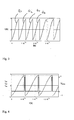
- Fig. 3 shows currents during a switched-on state of the switching transistors Q1, Q2 as the ignition voltage is developing in the prior art embodiment of fig. 1 .
- Fig. 4 shows signals I1 during a switched-on state of the switching transistors Q1, Q2 over a current path 105 while Q1 is on, and I2 over a current path 107 while Q2 is on, in the embodiment of fig. 2 according to the invention as the ignition voltage is developing.
- a pulse form current Ik in fig. 4 represents the output of a current measuring comparator A1, which rises up when the current of either switching transistor Q1 or Q2 rises over a limit value 120 set for the control circuit 104 and indicated by a dashed line.
- the regulation setup according to the invention enables controlling the current even upon the saturation of a coil L1.
- the coil L1 is depicted in a distributed fashion as coils L1a, L1b and L1c.
- Fig. 4 illustrates said currents I1 and I2 of the switching transistors Q1 and Q2, which are proportional to the voltage of a CS pin marked in figs. 2 and 5 in the size ratio of the resistors R8 and R10.
- Designated in fig. 4 is also a reference voltage Vcomp. of the current measuring comparator A1. When this reference voltage is crossed, there will be a change in the output state of the current measuring comparator A1.
- Fig. 5 shows an implementation according to a preferred embodiment of the invention for establishing a pulse-by-pulse current restriction for the switching transistors Q 1 and Q 2 .
- Fig. 6 shows oscillator signals relevant to the preferred embodiment of the invention shown in fig. 5 .
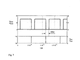
- Fig. 7 shows control signals for the switching transistors Q1, Q2 and output signals for a distribution circuit 116, also relevant to fig. 5 .
- an oscillator comparator A 2 functions as a monitor for the voltage between a capacitor C f and a resistor R f .
- the comparator A 2 triggers an RS flip-flop 121.
- the output of the flip-flop 121 rises up and the capacitor C f is charged by a transistor Q 4 back to a circuit operating voltage V cc .
- the flip-flop output also controls the divider circuit 116, whose complemented outputs operate at a frequency which is half of that of an oscillator circuit 114.
- the lamp ballast 102 has its circuitry maintained at a frequency level which is higher than it would be if defined solely by the resistor R f and the capacitor C f . This enables reaching a status in which the lamp ignition voltage maintains a constant level, even in the event that the coil L1 (L1A, LIB, L1C) of the lamp circuit becomes saturated.
- fig. 6 illustrates the signals of the oscillator circuit 114 when operating within a current restriction range of the switching transistors Q1, Q2, preferably set for the control circuit 104. Relating also to fig. 5 , there is shown in fig.
- the lamp comprises some of its circuit implementations in the form of an IC circuit (Integrated Circuits) and, in combination therewith, the rest of its circuit implementation in the form of at least one different circuit topology.
- the IC circuit Integrated circuits
- RC oscillator resistor-capacitor oscillator
- IC circuits are generally prefabricated entities with other circuitry connected to the inputs and/or outputs thereof. Aspects of the invention can also be carried out with any type of circuit topology, such as for example discrete components, ASIC circuits (Application Specific Integrated Circuits) or IC circuits or various combinations thereof.
- the lamp can be for example a fluorescent lamp or an HID lamp, i.e. a high intensity discharge lamp.
Landscapes
- Circuit Arrangements For Discharge Lamps (AREA)
Abstract
Description
- Tubular fluorescent lamps and HID lamps (High Intensity Discharge) are connected by way of electronic ballasts with a supply of electric power, receiving therefrom the energy needed thereby for illumination while being switched to the ON state.
- The fluorescent tube of fluorescent lamps and HID lamps is filled with a gas, such as for example argon or krypton. The generation of light further requires "a drop" of mercury which gasifies in response to an electrical discharge, producing ultraviolet radiation as electricity discharges through the fluorescent lamp tube. The fluorescent lamp tube has its inner surface coated with a fluorescent material, converting the ultraviolet radiation, which has been generated by the electrical discharge taking place in mercury vapor, into visible light.
- In addition to a fluorescent tube, the fluorescent lamp and the HID lamp comprise either an electronic ballast or a magnetic inductor. At present, magnetic inductors have been almost completely displaced by electronic ballasts. The current generated in electronic ballasts and flowing through a fluorescent lamp tube is generally 20-100 kHz in frequency, most typically 50-60 kHz.
- Measuring the current of a switching transistor set against earth potential represents prior known technology on the basis of several examples. In fact, this particular method has been and is currently used in a multitude of electronic ballasts available in the marketplace. Publication
WO2005/083872A1 comprises measuring the current of a first switching transistor set against earth potential, as well as the voltage of a midpoint between two switching transistors. However, no information can be obtained from this particular voltage about the current of a second switching transistor which is not set against earth potential. Accordingly, the signal produced in the process of measuring the voltage of said midpoint cannot be used as a signal on the basis of which said second switching transistor would be switched off in the event that its current exceeds a predetermined limit value. -
Fig 1 shows a lamp according to the Finnish patent application20075702 control circuit 104 integrated therewith so as to enable a measurement for providing separate measuring signals representing the currents of both an upper switching transistor Q1 and a lower switching transistor Q2. The embodiment shown infig. 1 features a diode couple Q3a and Q3b, which enables a measurement of the current for an ignition capacitor C1 and measurements of the currents for the switching transistors Q1 and Q2 with one resistor R3. Drawbacks in this embodiment include slowness in the establishment of measuring signals and thereby also in the status transitions of switching transistors based on said measuring signals, and instability in the magnitude of an ignition voltage established for the lamp. Another drawback in this embodiment is that, especially with large manufacturing volumes in mass production, the cost of diodes becomes high. - An objective of the invention is to provide an electronic ballast assembly, which enables establishing a lamp ignition voltage in a rapid and controlled fashion. This is achieved with a lamp according to the invention for producing illuminating radiation, comprising an electronic ballast for establishing an ignition voltage for the lamp in order to initiate the production of illuminating radiation, said electronic ballast comprising at least two switching transistors Q1, Q2 for supplying current to at least one coil, which develops the lamp ignition voltage, and said electronic ballast having a control circuit integrated therewith. The electronic ballast comprises at least two resistors R8, R10 set in a series connection at least relative to each other for measuring and/or regulating the currents of said at least two switching transistors Q1, Q2, said resistor R8 being in connection with the switching transistor Q2, and the resistor R10 being in a series connection with the resistorR8 and with a voltage source, and said electronic ballast comprising the series connection of said resistors R8, R10 for operating said control circuit in order to detect whether the current passing through the switching transistor Q1 or Q2 is overly high with respect to a limit current value set for the control circuit, and by operating said control circuit, for immediately switching off the control of that switching transistor Q1 or Q2 which switching transistor Q1 or Q2 has been found to have an overly high passing current and for immediately switching on the current of the other switching transistor Q1 or Q2.
- The invention is based on having the electronic ballast comprise at least two resistors R8, R10 set in a series connection relative to each other for measuring and/or regulating the currents of at least two switching transistors Q1, Q2 in such a way that the resistor R8 is in connection with the switching transistor Q2 and the resistor R10 is in a series connection with the resistor R8 and with a voltage source. This enables the elimination of a prior art diode connection, along with drawbacks associated therewith.
- An advantage of the invention is that the establishment of a lamp ignition voltage is expedited in a stable manner. The invention provides economic benefit in terms of the manufacturing costs of ballasts.
-
- Fig. 1
- shows a lamp according to the prior art described in patent application
FI20075702 - Fig. 2
- shows a lamp according to the invention.
- Fig. 3
- shows currents of the switching transistors Q1 and Q2 during the establishment of an ignition voltage in an embodiment according to the prior art.
- Fig. 4
- shows signals in an embodiment according to the invention during the establishment of an ignition voltage.
- Fig. 5
- shows an implementation according to a preferred embodiment of the invention pulse by pulse of the switching transistors Q1 and Q2 for establishing a current restriction.
- Fig. 6
- shows oscillator signals in a preferred embodiment of the invention.
- Fig. 7
- shows control signals for switching transistors and divider circuit output signals in a preferred embodiment of the invention.
-
Fig. 2 shows a lamp of the invention, which enables measuring a peak current for both switching transistors Q1, Q2 and controlling the current pulse by pulse in such a way that, during the establishment of an ignition voltage for the lamp, the current remains essentially constant. As opposed to a prior art lamp shown infig. 1 , the lamp according to the invention makes use of a series connection of the resistors R8 and R10 to establish connections, on the basis of which the prior art use of diodes is replaced by a configuration of improved performance. - The lamp according to the invention, as shown in
fig. 2 , includes an electronic ballast 102 comprising the resistors R8, R10 set in a series connection relative to each other for measuring and/or regulating the currents of the switching transistors Q1, Q2. The resistor R8 is in connection with the switching transistor Q2 and with acomparator connection 112 included in acontrol circuit 104. The resistor R10 is in a series connection with the resistor R8 and with a voltage source Vbus. The electronic ballast 102 comprises the series connection of said resistors R8, R10 for operating thecontrol circuit 104 through the intermediary of thecomparator connection 112 for detecting whether an overly high current is passing through the switching transistor Q1 or Q2 to thecontrol circuit 104. In this case, thecontrol circuit 104 is operated for immediately switching off the control of that switching transistor Q1 or Q2 which switching transistor Q1 or Q2 has been found to have an overly high passing current and for immediately switching on the current of the other switching transistor Q1 or Q2. In the process of switching on and during the switched-on period, the switching transistor Q1 or Q2 is supplied for example with a current in pulse form. A current path 107 represents the route of current in the process of establishing a lamp ignition voltage preceding the lamp ignition as the switching transistor Q2 is supplied with a current in pulse form. -
Fig. 3 shows currents during a switched-on state of the switching transistors Q1, Q2 as the ignition voltage is developing in the prior art embodiment offig. 1 .Fig. 4 shows signals I1 during a switched-on state of the switching transistors Q1, Q2 over acurrent path 105 while Q1 is on, and I2 over a current path 107 while Q2 is on, in the embodiment offig. 2 according to the invention as the ignition voltage is developing. A pulse form current Ik infig. 4 represents the output of a current measuring comparator A1, which rises up when the current of either switching transistor Q1 or Q2 rises over alimit value 120 set for thecontrol circuit 104 and indicated by a dashed line. The regulation setup according to the invention enables controlling the current even upon the saturation of a coil L1. Infigs. 2 and5 , the coil L1 is depicted in a distributed fashion as coils L1a, L1b and L1c.Fig. 4 illustrates said currents I1 and I2 of the switching transistors Q1 and Q2, which are proportional to the voltage of a CS pin marked infigs. 2 and5 in the size ratio of the resistors R8 and R10. Designated infig. 4 is also a reference voltage Vcomp. of the current measuring comparator A1. When this reference voltage is crossed, there will be a change in the output state of the current measuring comparator A1. -
Fig. 5 shows an implementation according to a preferred embodiment of the invention for establishing a pulse-by-pulse current restriction for the switching transistors Q1 and Q2. -
Fig. 6 shows oscillator signals relevant to the preferred embodiment of the invention shown infig. 5 . -
Fig. 7 shows control signals for the switching transistors Q1, Q2 and output signals for adistribution circuit 116, also relevant tofig. 5 . In the circuitry depicted infig. 5 , an oscillator comparator A2 functions as a monitor for the voltage between a capacitor Cf and a resistor Rf. When the resistor Rf discharges the charge of the capacitor Cf and the voltage falls below a reference Vref2, the comparator A2 triggers an RS flip-flop 121. Thus, the output of the flip-flop 121 rises up and the capacitor Cf is charged by a transistor Q4 back to a circuit operating voltage Vcc. The flip-flop output also controls thedivider circuit 116, whose complemented outputs operate at a frequency which is half of that of an oscillator circuit 114. - In further reference to
figs. 5, 6 and7 , with the current measuring comparator A1 in its active state, i.e. when the current limit set for the switching transistors Q1 and Q2 has been crossed, the negative input of the oscillator comparator A2 is pulled down by the current measuring comparator A1 through the intermediary of a transistor Q3 and the RS flip-flop 121 is triggered before the oscillator in a prior art solution would be triggered. Thus, in a preferred embodiment of the invention, the lamp ballast 102 has its circuitry maintained at a frequency level which is higher than it would be if defined solely by the resistor Rf and the capacitor Cf. This enables reaching a status in which the lamp ignition voltage maintains a constant level, even in the event that the coil L1 (L1A, LIB, L1C) of the lamp circuit becomes saturated. - With regard to what is depicted in
fig. 5 , there is shown infig. 6 a negative input or an input signal for the oscillator comparator A2 as said input signal of oscillator comparator A2 is driven downward by the output of the current measuring comparator A1 after the limit current value has been crossed, i.e. in other words,fig. 6 illustrates the signals of the oscillator circuit 114 when operating within a current restriction range of the switching transistors Q1, Q2, preferably set for thecontrol circuit 104. Relating also tofig. 5 , there is shown infig. 7 output voltages Vdiv1, Vdiv2 for thedivider circuit 116, and control voltages VdrvQ1, VdrvQ2 for the switching transistors which contain a dead time between a switch-off moment of the first switching transistor Q1 or Q2 and a switch-on moment of the second switching transistor Q1 or Q2. - The lamp comprises some of its circuit implementations in the form of an IC circuit (Integrated Circuits) and, in combination therewith, the rest of its circuit implementation in the form of at least one different circuit topology. The IC circuit (Integrated circuits) can be provided for example in the form of a resistor-capacitor oscillator (RC oscillator). IC circuits are generally prefabricated entities with other circuitry connected to the inputs and/or outputs thereof. Aspects of the invention can also be carried out with any type of circuit topology, such as for example discrete components, ASIC circuits (Application Specific Integrated Circuits) or IC circuits or various combinations thereof.
- Although the invention has been described in the foregoing specification with reference to circuit diagrams and signal examples illustrated in the figures, the invention is not limited to the circuit diagrams and signal examples presented in the specification and figures, but the invention can be varied within the scope defined in the appended claims. One notable example is that the order of a capacitor Cdc and a fluorescent tube 100 in the series connection can be other than what is illustrated without the reversal having any essential effect on the functionality of this embodiment of the invention. Respectively, other circuit combinations and component types existing within the limits defined by the appended claims can also be applicable as implementations according to the invention. In various embodiments of the invention, the lamp can be for example a fluorescent lamp or an HID lamp, i.e. a high intensity discharge lamp.
Claims (7)
- A lamp for producing illuminating radiation, said lamp comprising an electronic ballast (102) for establishing an ignition voltage for the lamp in order to initiate the production of illuminating radiation, said electronic ballast (102) comprising at least two switching transistors (Q1, Q2) for supplying current to at least one coil (L1) which develops the lamp ignition voltage, and the electronic ballast (102) having a control circuit (104) integrated therewith, characterized in that the electronic ballast (102) comprises at least two resistors R8 and R10 arranged at least in a series connection relative to each other for measuring and/or regulating the currents of said at least two switching transistors Q1 and Q2, said resistor R8 being in connection with the switching transistor Q2 and the resistor R10 being in a series connection with the resistor R8 and with a voltage source, and said electronic ballast (102) comprising the series connection of said resistors R8 and R10 for operating said control circuit (104) in order to detect whether a current passing through the switching transistor Q1 or Q2 is overly high with respect to a limit current value set for the control circuit, and by operating said control circuit (104), for immediately switching off the control of that switching transistor Q1 or Q2 which switching transistor Q1 or Q2 has been found with an overly high passing current and for immediately switching on the current of the other switching transistor Q1 or Q2.
- A lamp according to claim 1, characterized in that the lamp is a fluorescent lamp.
- A lamp according to claim 1, characterized in that the lamp is an HID (High Intensity Discharge) lamp.
- A lamp according to claim 1, characterized in that the control circuit (104) comprises a comparator connection (112) coupled with the resistor R8 for maintaining the lamp ignition voltage in a substantially constant magnitude, said comparator connection comprising a current measuring comparator A1 coupled with the resistor R8 and a transistor Q3 coupled with the current measuring comparator A1 by way of a resistor R11.
- A lamp according to claim 3, characterized in that the electronic ballast (102) comprises said comparator connection (112) coupled with the resistor R8 for maintaining the lamp ignition voltage in a substantially constant intensity in the event that the at least one coil L1, comprised by the electronic ballast (102), becomes essentially saturated.
- A lamp according to claim 1, characterized in that the lamp comprises some of its circuit configurations in the form of an IC circuit (Integrated Circuits), and in combination therewith, the rest of its circuit implementation in the form of at least one different circuit topology.
- A lamp according to claim 6, characterized in that the lamp comprises, functioning as an IC circuit (Integrated Circuits), a resistor-capacitor oscillator (RC oscillator).
Applications Claiming Priority (1)
| Application Number | Priority Date | Filing Date | Title |
|---|---|---|---|
| FI20095737A FI121561B (en) | 2009-06-30 | 2009-06-30 | Adjusting and measuring the functions of the electronic ballast |
Publications (3)
| Publication Number | Publication Date |
|---|---|
| EP2271187A2 true EP2271187A2 (en) | 2011-01-05 |
| EP2271187A3 EP2271187A3 (en) | 2013-03-20 |
| EP2271187B1 EP2271187B1 (en) | 2017-04-19 |
Family
ID=40825442
Family Applications (1)
| Application Number | Title | Priority Date | Filing Date |
|---|---|---|---|
| EP10163702.3A Not-in-force EP2271187B1 (en) | 2009-06-30 | 2010-05-24 | Controlling and measuring the functions of an electronic ballast |
Country Status (2)
| Country | Link |
|---|---|
| EP (1) | EP2271187B1 (en) |
| FI (1) | FI121561B (en) |
Citations (1)
| Publication number | Priority date | Publication date | Assignee | Title |
|---|---|---|---|---|
| WO2005083872A1 (en) | 2004-03-01 | 2005-09-09 | Tridonicatco Gmbh & Co. Kg | Current overload and voltage detection in a central point |
Family Cites Families (17)
| Publication number | Priority date | Publication date | Assignee | Title |
|---|---|---|---|---|
| JPH0650677B2 (en) | 1985-01-24 | 1994-06-29 | 松下電工株式会社 | Discharge lamp lighting device |
| US4873471A (en) | 1986-03-28 | 1989-10-10 | Thomas Industries Inc. | High frequency ballast for gaseous discharge lamps |
| DE4018127A1 (en) | 1990-06-06 | 1991-12-12 | Zumtobel Ag | METHOD AND CIRCUIT FOR CONTROLLING THE BRIGHTNESS (DIMMING) OF GAS DISCHARGE LAMPS |
| WO1999034647A1 (en) | 1997-12-23 | 1999-07-08 | Tridonic Bauelemente Gmbh | Method and device for detecting the rectification effect occurring in a gas-discharge lamp |
| DE20221985U1 (en) | 2002-02-01 | 2010-03-04 | Tridonicatco Gmbh & Co. Kg | Electronic ballast for gas discharge lamp |
| DE10205896A1 (en) | 2002-02-13 | 2003-09-04 | Patent Treuhand Ges Fuer Elektrische Gluehlampen Mbh | Operating circuit for discharge lamp with variable-frequency ignition |
| DE10221450A1 (en) | 2002-05-15 | 2003-11-27 | Philips Intellectual Property | Resonance converter circuit has a pair of switching stages operated by a controller to generate a chopper voltage that is applied to a rectifier |
| DE10223977C1 (en) | 2002-05-29 | 2003-09-04 | Siemens Ag | Current measuring circuit for controlling multi-phase electric motor uses 2 measuring transducers with offset inputs coupled to combining stage providing overall output |
| US6891339B2 (en) | 2002-09-19 | 2005-05-10 | International Rectifier Corporation | Adaptive CFL control circuit |
| DE602004007357T2 (en) | 2003-02-04 | 2008-03-06 | Koninklijke Philips Electronics N.V. | CIRCUIT |
| WO2006003560A1 (en) | 2004-06-28 | 2006-01-12 | Koninklijke Philips Electronics N.V. | Fluorescent tube lamp drive circuit |
| DE102004037389C5 (en) | 2004-08-02 | 2014-04-10 | Infineon Technologies Ag | Method for controlling a load having a fluorescent lamp for optimizing the ignition process |
| US7288898B2 (en) | 2005-03-04 | 2007-10-30 | International Rectifier Corporation | Automotive high intensity discharge lamp ballast circuit |
| DE102005020178A1 (en) | 2005-04-28 | 2006-11-09 | HÜCO electronic GmbH | Switching device for high pressure gas discharge lamp operation, has measuring device that stands in connection with frequency control unit such that power inverter circuit is controlled dependent on measured resonance parameter |
| EP1776000A3 (en) | 2005-10-12 | 2008-05-28 | Int Rectifier Corp | 8-Pin PFC and ballast control IC |
| CN101277571B (en) | 2007-03-30 | 2014-02-12 | 电灯专利信托有限公司 | Ignition control method for discharge lamp as well as corresponding electronic ballast circuit |
| FI121049B (en) | 2007-10-04 | 2010-06-15 | Helvar Oy Ab | Electronic ballast |
-
2009
- 2009-06-30 FI FI20095737A patent/FI121561B/en not_active IP Right Cessation
-
2010
- 2010-05-24 EP EP10163702.3A patent/EP2271187B1/en not_active Not-in-force
Patent Citations (1)
| Publication number | Priority date | Publication date | Assignee | Title |
|---|---|---|---|---|
| WO2005083872A1 (en) | 2004-03-01 | 2005-09-09 | Tridonicatco Gmbh & Co. Kg | Current overload and voltage detection in a central point |
Also Published As
| Publication number | Publication date |
|---|---|
| FI20095737A0 (en) | 2009-06-30 |
| EP2271187B1 (en) | 2017-04-19 |
| EP2271187A3 (en) | 2013-03-20 |
| FI121561B (en) | 2010-12-31 |
Similar Documents
| Publication | Publication Date | Title |
|---|---|---|
| KR100899490B1 (en) | Dc/ac converter, its controller ic and control device | |
| EP1729549B1 (en) | High voltage discharge lamp lighting apparatus and luminaire | |
| JP5051862B1 (en) | Straight tube type light emitting diode lighting | |
| KR100983703B1 (en) | DC-AC converter and AC power supply method | |
| US6285138B1 (en) | Apparatus for lighting fluorescent lamp | |
| JP2004134360A (en) | Ballast for three-way dimming compact fluorescent lamp | |
| JP2010283998A (en) | Resonance inverter driving method using zero-current switching and pulse width modulation of arbitrary frequency | |
| JP2000507036A (en) | ballast | |
| EP2282616A1 (en) | High-voltage discharge lamp operation device and illumination instrument | |
| CN101389174A (en) | Inverter and control circuit, control method and luminescent device using the same | |
| RU2609130C2 (en) | Driver for connecting light-emitting diode to electronic ballast | |
| JP4116092B2 (en) | Circuit arrangement for dimmable operation of a fluorescent lamp | |
| JP4186801B2 (en) | Electrodeless discharge lamp lighting device and electrodeless discharge lamp device | |
| KR20040016666A (en) | Driving apparatus and method of inverter | |
| WO2009107057A1 (en) | Dimming circuit and electronic ballast for a lamp | |
| US8742670B2 (en) | Electronic ballast | |
| JP4797511B2 (en) | Cold cathode tube lighting device, tube current control method, and integrated circuit | |
| EP2271187B1 (en) | Controlling and measuring the functions of an electronic ballast | |
| CN101902868A (en) | Operating a resonant load circuit, a dimming circuit, and a dimming method | |
| JP4182081B2 (en) | Discharge lamp driving device | |
| WO2010054454A2 (en) | Electronic ballast for metal vapor lamps using integration techniques for power factor correction and acoustic resonance elimination | |
| JP3448904B2 (en) | Lighting device for dimming | |
| CN101496453A (en) | Method and circuit for heating electrodes of a discharge lamp | |
| Lin et al. | Design and implementation of electronic ballast for electrodeless fluorescent lamp with primary-side control | |
| JP4966122B2 (en) | Discharge lamp lighting device and lighting fixture |
Legal Events
| Date | Code | Title | Description |
|---|---|---|---|
| PUAI | Public reference made under article 153(3) epc to a published international application that has entered the european phase |
Free format text: ORIGINAL CODE: 0009012 |
|
| AK | Designated contracting states |
Kind code of ref document: A2 Designated state(s): AL AT BE BG CH CY CZ DE DK EE ES FI FR GB GR HR HU IE IS IT LI LT LU LV MC MK MT NL NO PL PT RO SE SI SK SM TR |
|
| AX | Request for extension of the european patent |
Extension state: BA ME RS |
|
| PUAL | Search report despatched |
Free format text: ORIGINAL CODE: 0009013 |
|
| AK | Designated contracting states |
Kind code of ref document: A3 Designated state(s): AL AT BE BG CH CY CZ DE DK EE ES FI FR GB GR HR HU IE IS IT LI LT LU LV MC MK MT NL NO PL PT RO SE SI SK SM TR |
|
| AX | Request for extension of the european patent |
Extension state: BA ME RS |
|
| RIC1 | Information provided on ipc code assigned before grant |
Ipc: H05B 41/292 20060101ALI20130208BHEP Ipc: H05B 41/285 20060101ALI20130208BHEP Ipc: H05B 41/282 20060101AFI20130208BHEP Ipc: H05B 41/298 20060101ALI20130208BHEP |
|
| 17P | Request for examination filed |
Effective date: 20130912 |
|
| RBV | Designated contracting states (corrected) |
Designated state(s): AL AT BE BG CH CY CZ DE DK EE ES FI FR GB GR HR HU IE IS IT LI LT LU LV MC MK MT NL NO PL PT RO SE SI SK SM TR |
|
| GRAP | Despatch of communication of intention to grant a patent |
Free format text: ORIGINAL CODE: EPIDOSNIGR1 |
|
| INTG | Intention to grant announced |
Effective date: 20161026 |
|
| GRAJ | Information related to disapproval of communication of intention to grant by the applicant or resumption of examination proceedings by the epo deleted |
Free format text: ORIGINAL CODE: EPIDOSDIGR1 |
|
| STAA | Information on the status of an ep patent application or granted ep patent |
Free format text: STATUS: REQUEST FOR EXAMINATION WAS MADE |
|
| GRAR | Information related to intention to grant a patent recorded |
Free format text: ORIGINAL CODE: EPIDOSNIGR71 |
|
| GRAS | Grant fee paid |
Free format text: ORIGINAL CODE: EPIDOSNIGR3 |
|
| STAA | Information on the status of an ep patent application or granted ep patent |
Free format text: STATUS: GRANT OF PATENT IS INTENDED |
|
| GRAA | (expected) grant |
Free format text: ORIGINAL CODE: 0009210 |
|
| STAA | Information on the status of an ep patent application or granted ep patent |
Free format text: STATUS: THE PATENT HAS BEEN GRANTED |
|
| INTC | Intention to grant announced (deleted) | ||
| RAP1 | Party data changed (applicant data changed or rights of an application transferred) |
Owner name: HELVAR OY AB |
|
| RIN1 | Information on inventor provided before grant (corrected) |
Inventor name: VIHINEN, HANNU |
|
| AK | Designated contracting states |
Kind code of ref document: B1 Designated state(s): AL AT BE BG CH CY CZ DE DK EE ES FI FR GB GR HR HU IE IS IT LI LT LU LV MC MK MT NL NO PL PT RO SE SI SK SM TR |
|
| INTG | Intention to grant announced |
Effective date: 20170313 |
|
| REG | Reference to a national code |
Ref country code: GB Ref legal event code: FG4D |
|
| RIN1 | Information on inventor provided before grant (corrected) |
Inventor name: VIHINEN, HANNU |
|
| REG | Reference to a national code |
Ref country code: CH Ref legal event code: EP |
|
| REG | Reference to a national code |
Ref country code: AT Ref legal event code: REF Ref document number: 887052 Country of ref document: AT Kind code of ref document: T Effective date: 20170515 |
|
| REG | Reference to a national code |
Ref country code: IE Ref legal event code: FG4D |
|
| REG | Reference to a national code |
Ref country code: DE Ref legal event code: R096 Ref document number: 602010041604 Country of ref document: DE |
|
| REG | Reference to a national code |
Ref country code: NL Ref legal event code: MP Effective date: 20170419 |
|
| REG | Reference to a national code |
Ref country code: LT Ref legal event code: MG4D |
|
| REG | Reference to a national code |
Ref country code: AT Ref legal event code: MK05 Ref document number: 887052 Country of ref document: AT Kind code of ref document: T Effective date: 20170419 |
|
| PG25 | Lapsed in a contracting state [announced via postgrant information from national office to epo] |
Ref country code: NL Free format text: LAPSE BECAUSE OF FAILURE TO SUBMIT A TRANSLATION OF THE DESCRIPTION OR TO PAY THE FEE WITHIN THE PRESCRIBED TIME-LIMIT Effective date: 20170419 |
|
| PG25 | Lapsed in a contracting state [announced via postgrant information from national office to epo] |
Ref country code: ES Free format text: LAPSE BECAUSE OF FAILURE TO SUBMIT A TRANSLATION OF THE DESCRIPTION OR TO PAY THE FEE WITHIN THE PRESCRIBED TIME-LIMIT Effective date: 20170419 Ref country code: LT Free format text: LAPSE BECAUSE OF FAILURE TO SUBMIT A TRANSLATION OF THE DESCRIPTION OR TO PAY THE FEE WITHIN THE PRESCRIBED TIME-LIMIT Effective date: 20170419 Ref country code: AT Free format text: LAPSE BECAUSE OF FAILURE TO SUBMIT A TRANSLATION OF THE DESCRIPTION OR TO PAY THE FEE WITHIN THE PRESCRIBED TIME-LIMIT Effective date: 20170419 Ref country code: GR Free format text: LAPSE BECAUSE OF FAILURE TO SUBMIT A TRANSLATION OF THE DESCRIPTION OR TO PAY THE FEE WITHIN THE PRESCRIBED TIME-LIMIT Effective date: 20170720 Ref country code: FI Free format text: LAPSE BECAUSE OF FAILURE TO SUBMIT A TRANSLATION OF THE DESCRIPTION OR TO PAY THE FEE WITHIN THE PRESCRIBED TIME-LIMIT Effective date: 20170419 Ref country code: HR Free format text: LAPSE BECAUSE OF FAILURE TO SUBMIT A TRANSLATION OF THE DESCRIPTION OR TO PAY THE FEE WITHIN THE PRESCRIBED TIME-LIMIT Effective date: 20170419 Ref country code: NO Free format text: LAPSE BECAUSE OF FAILURE TO SUBMIT A TRANSLATION OF THE DESCRIPTION OR TO PAY THE FEE WITHIN THE PRESCRIBED TIME-LIMIT Effective date: 20170719 |
|
| PG25 | Lapsed in a contracting state [announced via postgrant information from national office to epo] |
Ref country code: PL Free format text: LAPSE BECAUSE OF FAILURE TO SUBMIT A TRANSLATION OF THE DESCRIPTION OR TO PAY THE FEE WITHIN THE PRESCRIBED TIME-LIMIT Effective date: 20170419 Ref country code: SE Free format text: LAPSE BECAUSE OF FAILURE TO SUBMIT A TRANSLATION OF THE DESCRIPTION OR TO PAY THE FEE WITHIN THE PRESCRIBED TIME-LIMIT Effective date: 20170419 Ref country code: IS Free format text: LAPSE BECAUSE OF FAILURE TO SUBMIT A TRANSLATION OF THE DESCRIPTION OR TO PAY THE FEE WITHIN THE PRESCRIBED TIME-LIMIT Effective date: 20170819 Ref country code: LV Free format text: LAPSE BECAUSE OF FAILURE TO SUBMIT A TRANSLATION OF THE DESCRIPTION OR TO PAY THE FEE WITHIN THE PRESCRIBED TIME-LIMIT Effective date: 20170419 Ref country code: BG Free format text: LAPSE BECAUSE OF FAILURE TO SUBMIT A TRANSLATION OF THE DESCRIPTION OR TO PAY THE FEE WITHIN THE PRESCRIBED TIME-LIMIT Effective date: 20170719 |
|
| REG | Reference to a national code |
Ref country code: CH Ref legal event code: PL |
|
| REG | Reference to a national code |
Ref country code: DE Ref legal event code: R026 Ref document number: 602010041604 Country of ref document: DE |
|
| PLBI | Opposition filed |
Free format text: ORIGINAL CODE: 0009260 |
|
| PG25 | Lapsed in a contracting state [announced via postgrant information from national office to epo] |
Ref country code: MC Free format text: LAPSE BECAUSE OF FAILURE TO SUBMIT A TRANSLATION OF THE DESCRIPTION OR TO PAY THE FEE WITHIN THE PRESCRIBED TIME-LIMIT Effective date: 20170419 Ref country code: SK Free format text: LAPSE BECAUSE OF FAILURE TO SUBMIT A TRANSLATION OF THE DESCRIPTION OR TO PAY THE FEE WITHIN THE PRESCRIBED TIME-LIMIT Effective date: 20170419 Ref country code: CZ Free format text: LAPSE BECAUSE OF FAILURE TO SUBMIT A TRANSLATION OF THE DESCRIPTION OR TO PAY THE FEE WITHIN THE PRESCRIBED TIME-LIMIT Effective date: 20170419 Ref country code: DK Free format text: LAPSE BECAUSE OF FAILURE TO SUBMIT A TRANSLATION OF THE DESCRIPTION OR TO PAY THE FEE WITHIN THE PRESCRIBED TIME-LIMIT Effective date: 20170419 Ref country code: EE Free format text: LAPSE BECAUSE OF FAILURE TO SUBMIT A TRANSLATION OF THE DESCRIPTION OR TO PAY THE FEE WITHIN THE PRESCRIBED TIME-LIMIT Effective date: 20170419 Ref country code: RO Free format text: LAPSE BECAUSE OF FAILURE TO SUBMIT A TRANSLATION OF THE DESCRIPTION OR TO PAY THE FEE WITHIN THE PRESCRIBED TIME-LIMIT Effective date: 20170419 |
|
| PLAX | Notice of opposition and request to file observation + time limit sent |
Free format text: ORIGINAL CODE: EPIDOSNOBS2 |
|
| REG | Reference to a national code |
Ref country code: IE Ref legal event code: MM4A |
|
| 26 | Opposition filed |
Opponent name: TRIDONIC GMBH & CO KG Effective date: 20180118 |
|
| PG25 | Lapsed in a contracting state [announced via postgrant information from national office to epo] |
Ref country code: CH Free format text: LAPSE BECAUSE OF NON-PAYMENT OF DUE FEES Effective date: 20170531 Ref country code: IT Free format text: LAPSE BECAUSE OF FAILURE TO SUBMIT A TRANSLATION OF THE DESCRIPTION OR TO PAY THE FEE WITHIN THE PRESCRIBED TIME-LIMIT Effective date: 20170419 Ref country code: SM Free format text: LAPSE BECAUSE OF FAILURE TO SUBMIT A TRANSLATION OF THE DESCRIPTION OR TO PAY THE FEE WITHIN THE PRESCRIBED TIME-LIMIT Effective date: 20170419 Ref country code: LI Free format text: LAPSE BECAUSE OF NON-PAYMENT OF DUE FEES Effective date: 20170531 |
|
| REG | Reference to a national code |
Ref country code: FR Ref legal event code: ST Effective date: 20180131 |
|
| GBPC | Gb: european patent ceased through non-payment of renewal fee |
Effective date: 20170719 |
|
| PG25 | Lapsed in a contracting state [announced via postgrant information from national office to epo] |
Ref country code: LU Free format text: LAPSE BECAUSE OF NON-PAYMENT OF DUE FEES Effective date: 20170524 |
|
| REG | Reference to a national code |
Ref country code: BE Ref legal event code: MM Effective date: 20170531 |
|
| PG25 | Lapsed in a contracting state [announced via postgrant information from national office to epo] |
Ref country code: GB Free format text: LAPSE BECAUSE OF NON-PAYMENT OF DUE FEES Effective date: 20170719 Ref country code: IE Free format text: LAPSE BECAUSE OF NON-PAYMENT OF DUE FEES Effective date: 20170524 |
|
| PG25 | Lapsed in a contracting state [announced via postgrant information from national office to epo] |
Ref country code: FR Free format text: LAPSE BECAUSE OF NON-PAYMENT OF DUE FEES Effective date: 20170619 Ref country code: SI Free format text: LAPSE BECAUSE OF FAILURE TO SUBMIT A TRANSLATION OF THE DESCRIPTION OR TO PAY THE FEE WITHIN THE PRESCRIBED TIME-LIMIT Effective date: 20170419 |
|
| PLBB | Reply of patent proprietor to notice(s) of opposition received |
Free format text: ORIGINAL CODE: EPIDOSNOBS3 |
|
| PG25 | Lapsed in a contracting state [announced via postgrant information from national office to epo] |
Ref country code: BE Free format text: LAPSE BECAUSE OF NON-PAYMENT OF DUE FEES Effective date: 20170531 |
|
| PG25 | Lapsed in a contracting state [announced via postgrant information from national office to epo] |
Ref country code: MT Free format text: LAPSE BECAUSE OF NON-PAYMENT OF DUE FEES Effective date: 20170524 |
|
| RDAF | Communication despatched that patent is revoked |
Free format text: ORIGINAL CODE: EPIDOSNREV1 |
|
| PLCK | Communication despatched that opposition was rejected |
Free format text: ORIGINAL CODE: EPIDOSNREJ1 |
|
| PG25 | Lapsed in a contracting state [announced via postgrant information from national office to epo] |
Ref country code: HU Free format text: LAPSE BECAUSE OF FAILURE TO SUBMIT A TRANSLATION OF THE DESCRIPTION OR TO PAY THE FEE WITHIN THE PRESCRIBED TIME-LIMIT; INVALID AB INITIO Effective date: 20100524 |
|
| REG | Reference to a national code |
Ref country code: DE Ref legal event code: R100 Ref document number: 602010041604 Country of ref document: DE |
|
| PLBN | Opposition rejected |
Free format text: ORIGINAL CODE: 0009273 |
|
| STAA | Information on the status of an ep patent application or granted ep patent |
Free format text: STATUS: OPPOSITION REJECTED |
|
| PG25 | Lapsed in a contracting state [announced via postgrant information from national office to epo] |
Ref country code: CY Free format text: LAPSE BECAUSE OF NON-PAYMENT OF DUE FEES Effective date: 20170419 |
|
| 27O | Opposition rejected |
Effective date: 20190701 |
|
| PG25 | Lapsed in a contracting state [announced via postgrant information from national office to epo] |
Ref country code: MK Free format text: LAPSE BECAUSE OF FAILURE TO SUBMIT A TRANSLATION OF THE DESCRIPTION OR TO PAY THE FEE WITHIN THE PRESCRIBED TIME-LIMIT Effective date: 20170419 |
|
| PG25 | Lapsed in a contracting state [announced via postgrant information from national office to epo] |
Ref country code: TR Free format text: LAPSE BECAUSE OF FAILURE TO SUBMIT A TRANSLATION OF THE DESCRIPTION OR TO PAY THE FEE WITHIN THE PRESCRIBED TIME-LIMIT Effective date: 20170419 |
|
| PG25 | Lapsed in a contracting state [announced via postgrant information from national office to epo] |
Ref country code: PT Free format text: LAPSE BECAUSE OF FAILURE TO SUBMIT A TRANSLATION OF THE DESCRIPTION OR TO PAY THE FEE WITHIN THE PRESCRIBED TIME-LIMIT Effective date: 20170419 |
|
| PG25 | Lapsed in a contracting state [announced via postgrant information from national office to epo] |
Ref country code: AL Free format text: LAPSE BECAUSE OF FAILURE TO SUBMIT A TRANSLATION OF THE DESCRIPTION OR TO PAY THE FEE WITHIN THE PRESCRIBED TIME-LIMIT Effective date: 20170419 |
|
| PGFP | Annual fee paid to national office [announced via postgrant information from national office to epo] |
Ref country code: DE Payment date: 20230530 Year of fee payment: 14 |
|
| REG | Reference to a national code |
Ref country code: DE Ref legal event code: R119 Ref document number: 602010041604 Country of ref document: DE |
|
| PG25 | Lapsed in a contracting state [announced via postgrant information from national office to epo] |
Ref country code: DE Free format text: LAPSE BECAUSE OF NON-PAYMENT OF DUE FEES Effective date: 20241203 |