EP2268115A2 - Electronic Device - Google Patents
Electronic Device Download PDFInfo
- Publication number
- EP2268115A2 EP2268115A2 EP10160261A EP10160261A EP2268115A2 EP 2268115 A2 EP2268115 A2 EP 2268115A2 EP 10160261 A EP10160261 A EP 10160261A EP 10160261 A EP10160261 A EP 10160261A EP 2268115 A2 EP2268115 A2 EP 2268115A2
- Authority
- EP
- European Patent Office
- Prior art keywords
- terminal
- holder plate
- printed wiring
- wiring board
- face
- Prior art date
- Legal status (The legal status is an assumption and is not a legal conclusion. Google has not performed a legal analysis and makes no representation as to the accuracy of the status listed.)
- Granted
Links
Images
Classifications
-
- H—ELECTRICITY
- H05—ELECTRIC TECHNIQUES NOT OTHERWISE PROVIDED FOR
- H05K—PRINTED CIRCUITS; CASINGS OR CONSTRUCTIONAL DETAILS OF ELECTRIC APPARATUS; MANUFACTURE OF ASSEMBLAGES OF ELECTRICAL COMPONENTS
- H05K5/00—Casings, cabinets or drawers for electric apparatus
- H05K5/0017—Casings, cabinets or drawers for electric apparatus with operator interface units
Definitions
- the present invention generally relates to an electronic device. More specifically, the present invention relates to an electronic device having an electric terminal.
- a conventional liquid crystal television set includes a liquid crystal module, a cabinet, and a stand.
- the liquid crystal module is housed in the cabinet.
- the cabinet has a front cabinet and a rear cabinet.
- a synthetic resin holder plate is disposed in an opening formed in a side face of the cabinet.
- a plurality of terminal holes is formed in the holder plate. Connectors of an S-video terminal and RCA terminals are inserted into the respective terminal holes.
- the S-video terminal and the RCA terminals are fixed on a support board that includes a printed wiring board.
- a plurality of engagement tabs for gripping the end edge of the support board are integrally provided protruding from the rear face of the holder plate.
- a cylindrical part is integrally provided protruding from one side edge of the upper end face of the S-video terminal.
- a screw insertion hole for inserting a screw is formed in the holder plate opposite the cylindrical part.
- a pair of support bases is formed by stamping the chassis of the liquid crystal module. Threaded holes are formed in the tops of the support bases. Screw insertion holes for inserting screws are formed in the support board opposite thee threaded holes.
- the assembly procedure will now be described.
- the end edge of the support board is engaged by being plugged in between the engagement tabs.
- the support board is placed on the support bases.
- the connectors of the S-video terminal and the RCA terminals are inserted into the terminal holes of the holder plate.
- the screws are threaded through the screw insertion holes of the support board and into the threaded holes of the support bases, thereby fixing the support board to the chassis.
- a screw is threaded through the screw insertion hole of the holder plate and into the cylindrical part of the S-video terminal, which fixes the S-video terminal to the holder plate.
- the protrusion length of the connector of the S-video terminal is short.
- the connector is disposed in a state of being recessed in the terminal hole. Therefore, the plug is difficult to connect to the connector.
- the plug has to be connected by being pushed forcefully into the connector. This pushing force lifts up the S-video terminal away from the support board. Thus, there is the risk that the solder connecting the S-video terminal to the support board loosen and rattle, or that the soldering is damaged.
- the S-video terminal is fastened with the screw to the holder plate, which reinforces so that the S-video terminal does not move away from the support board.
- This entails the use of the screw, more parts are required. As a result, the cost is higher, and installing the screw requires more work.
- One object of the present invention is to provide an electronic device in which an electric terminal is secured with a simple and inexpensive structure.
- an electronic device includes a cabinet, a device main body, a printed wiring board, an electric terminal, and a holder plate.
- the device main body is disposed within the cabinet.
- the printed wiring board is electrically coupled to the device main body.
- the electric terminal is disposed on a first face of the printed wiring board.
- the electric terminal is electrically coupled to the printed wiring board.
- the electric terminal includes a terminal body and a connector.
- the holder plate is attached to the cabinet.
- the holder plate includes a terminal hole, first and second engagement portions, and a restricting portion.
- the connector of the electric terminal is disposed through the terminal hole.
- the first and second engagement portions extend from an inner face of the holder plate. The first engagement portion contacts with the first face of the printed wiring board.
- the second engagement portion contacts with a second face of the printed wiring board that is opposite the first face of the printed wiring board.
- the restricting portion extends from the inner face of the holder plate. The restricting portion faces a top face of the terminal body of the electric terminal in a direction perpendicular to the printed wiring board.
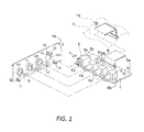
- FIG. 1 is an exploded perspective view of a terminal attachment structure of an electronic device in accordance with one embodiment
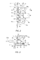
- FIG. 2 is a normal view of the terminal attachment structure illustrated in FIG. 1 ;
- FIG. 3 is a cross sectional view of the terminal attachment structure taken along III-III line in FIG. 2 ;
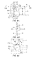
- FIG. 4A is an exploded enlarged cross sectional view of the terminal attachment structure
- FIG. 4B is a cross sectional view taken along IVB-IVB line in FIG. 4A ;
- FIG. 4C is a cross sectional view taken along IVC-IVC line in FIG. 4A ;
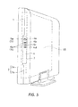
- FIG. 5 is a perspective view of the electronic device.
- FIG. 5 is a perspective view of an electronic device.
- the electronic device includes a liquid crystal television set.
- the electronic device includes a liquid crystal module (e.g., device main body) 1, a cabinet 2, a holder plate 4, an S-video terminal (e.g., electric terminal) 5, a plurality (e.g., three) of RCA terminals 6, and a stand 7.
- the liquid crystal module 1 is disposed within the cabinet 2.
- the liquid crystal module 1 mainly includes a liquid crystal panel (e.g., liquid crystal cell) to display image.
- the liquid crystal module also includes a chasse 15 that houses the liquid crystal panel.
- the cabinet 2 includes a front cabinet 2a and a rear cabinet 2b.
- the holder plate 4 is made of synthetic resin.
- the holder plate 4 is disposed in an opening (e.g., opening portion) 3 formed at a suitable location in a side face of the cabinet 2.
- a plurality (e.g., four) of terminal holes 4a to 4d is formed in the holder plate 4.
- the terminal holes 4a to 4d have an S-video terminal hole (e.g., S-video terminal-use terminal hole) 4a, and RCA terminal holes (RCA terminal-use terminal holes) 4b to 4d.
- the S-video terminal 5 includes a connector (e.g., socket) 5a and a terminal body 5b with an upper end face 5c.
- the RCA terminals 6 include connectors (e.g., sockets) 6a and terminal bodies 6b. The connectors 5a and 6a of the S-video terminal 5 and the RCA terminals 6 are inserted into the respective terminal holes 4a to 4d.
- the stand 7 is fixedly coupled to the cabinet 2.
- FIGS. 1 to 3 , and 4A to 4C show a terminal attachment structure of the electronic device.
- the terminal attachment structure of the electronic device includes the holder plate 4, the S-video terminal 5, and a support board (e.g., printed wiring board) 9.
- a support board e.g., printed wiring board
- the S-video terminal 5 and the RCA terminals 6 are fixed on an upper face 9a of the support board 9.
- the support board 9 includes a printed wiring board that is electrically coupled to the S-video terminal 5 and the RCA terminals 6.
- the support board 9 is also electrically connected with a control board 1a of the liquid crystal module 1 via a flexible flat cable 19.
- the holder plate 4 has a plurality of engagement tabs (e.g., first and second engagement portions) 10 and 11 for gripping end edge portion of the support board 9.
- the engagement tabs 10 and 11 are integrally provided protruding from a rear face (e.g., inner face) 4e of the holder plate 4.
- the engagement tabs 10 contact with the upper face 9a of the support board 9.
- the engagement tabs 11 contact with a lower face 9b of the support board 9 that is opposite to the upper face 9a.
- the chassis 15 of the liquid crystal module 1 has a pair of support bases 15a.
- the support bases 15a are formed by stamping the chassis 15 of the liquid crystal module 1.
- Threaded holes 17 are formed in top portions of the support bases 15a, respectively.
- Screw insertion holes 16 for inserting screws 18 are formed in the support board 9 opposite the threaded holes 17.
- the holder plate 4 further has a contact rib (e.g., restricting portion) 22, and a guide plate (e.g., guide portion) 23.
- the contact rib 22 is opposite the upper face 9a of the support board 9, with the S-video terminal hole 4a in between, at a spacing H that is the same as or slightly greater than the height h of the S-video terminal 5.
- the contact rib 22 is positioned at a location spaced apart from the upper face 9a by a distance that is equal to or greater than the height h of the terminal body 5b of the S-video terminal 5 measured in the direction perpendicular to the upper face 9a.
- the S-video terminal hole 4a is positioned between the contact rib 22 and the upper face 9a of the support board 9 in the direction perpendicular to the upper face 9a.
- the contact rib 22 is integrally provided protruding from the rear face 4e of the holder plate 4.
- the contact rib 22 faces the upper end face 5c of the terminal body 5b of the S-video terminal 5.
- the contact rib 22 contacts with the upper end face 5c.
- the contact rib 22 can be disposed at spaced apart location from the upper end face 5c with a small gap therebetween.
- the contact rib 22 is in the form of a slender plate.
- the contact rib 22 is disposed along an imaginary line M that passes through the center O of the S-video terminal hole 4a and traverses the holder plate 4 in the direction perpendicular to the upper face 9a of the support board 9.
- An S-video terminal-opposing face (e.g., bottom face) 22a of the contact rib 22 extends perpendicular to the rear face 4e of the holder plate 4.
- An arc face 22b is formed spreading outward toward the distal end of the contact rib 22 from the S-video terminal-opposing face 22a.
- the S-video terminal 5 is guided along the arc face 22b.
- the guide plate 23 extends along an imaginary line N that is perpendicular to the imaginary line M and is parallel to the upper end face 5c of the S-video terminal 5 and is in-plane with the S-video terminal-opposing face 22a of the contact rib 22.
- the guide plate 23 includes an S-video terminal-opposing face 23a.
- the S-video terminal-opposing faces 22a and 23a of the contact rib 22 and the guide plate 23 lie in a single plane.
- the guide plate 23 is integrally provided protruding from the rear face 4e of the holder plate 4 and the contact rib 22.
- the holder plate 4 is integrally formed with a one-piece, unitary member.
- the support board 9 is moved from the state indicated by the solid lines in FIG. 1 into the proximity of the holder plate 4.
- the upper end face 5c of the S-video terminal 5 is slid from the arc face 22b of the contact rib 22 along the guide plate 23 such that the upper end face 5c of the S-video terminal 5 is brought into contact or proximity with the contact rib 22.
- the connectors 5a and 6a of the S-video terminal 5 and the RCA terminals 6 are inserted into the terminal holes 4a to 4d, respectively, and the end edge portion of the support board 9 is plugged in and engaged between the engagement tabs 10 and 11 (see the imaginary lines in FIG. 1 ).
- the support board 9 is placed on the support bases 15a, and as shown in FIGS. 2 and 3 , the screws 18 are threaded into the threaded holes 17 of the support bases 15a through the screw insertion holes 16, thereby fixing the support board 9 to the chassis 15.
- a cord 20a when a cord 20a is connected to the S-video terminal 5, a plug 20 at the distal end of the cord 20a is grasped and pushed against and fitted together with the connector 5a of the S-video terminal 5.
- the cord 20a is electrically connected to another electric device, such as a disk recorder or player. Plugs with cords (not shown) are connected to the connectors 6a of the RCA terminals 6 by the same procedure.
- the protrusion length t of the connector 5a of the S-video terminal 5 relative to a front face of the terminal body 5b is short, and the connector 5a is disposed in a state of being recessed in the S-video terminal hole 4a.
- the plug 20 is connected by being pushed forcefully into the connector 5a of the S-video terminal 5.
- the contact rib 22 prevents this pushing force from lifting the S-video terminal 5 away from the support board 9.
- the state of the S-video terminal 5 being fixed to the support board 9 can be reliably maintained without the solder connecting the S-video terminal to the support board 9 loosening and rattling, or the soldering being damaged.
- the contact rib 22 is integrally provided protruding from the holder plate 4, there is no increase in the number of parts, and the cost can be reduced compared to when the S-video terminal 5 is fastened to the holder plate 4 with a screw. Also, since there is no screw insertion hole in the holder plate 4 for fastening the S-video terminal 5 to the holder plate 4, the appearance of the holder plate 4 can be improved.
- the S-video terminal 5 can be fixed at the specified location merely by engaging the end edge portion of the support board 9 with the engagement tabs 10 and 11 and fastening the support board 9 to the chassis 15 inside the cabinet 2.
- the assembly work can be carried out more quickly and easily than when the S-video terminal 5 is fastened to the holder plate 4 with a screw. Therefore, the S-video terminal 5 can be attached and fixed easily with a simple and inexpensive structure.
- the electronic device includes the liquid crystal television set.
- a liquid crystal television set that is convenient to use and allows the attachment and fixing of the S-video terminal 5 to be carried out easily with a simple and inexpensive structure.
- the connector 5a of the S-video terminal 5 can be reliably and easily inserted into the terminal hole 4a by sliding the S-video terminal 5 along the guide plate 23.
- a liquid crystal television set was given as an example in the above embodiment.
- the application of the terminal attachment structure is not limited to this. It can also be applied to any of various electronic devices equipped with an S-video terminal, such as a disk device (such as a Blu-ray Disc recorder or player).
- the contact rib 22 and the guide plate 23 can be formed for other type of electric terminals, such as the RCA terminals 6 and the like.
Landscapes
- Engineering & Computer Science (AREA)
- Microelectronics & Electronic Packaging (AREA)
- Coupling Device And Connection With Printed Circuit (AREA)
- Devices For Indicating Variable Information By Combining Individual Elements (AREA)
Abstract
Description
- This application claims priority to Japanese Patent Application No.
2009-101715 filed on April 20, 2009 2009-101715 - The present invention generally relates to an electronic device. More specifically, the present invention relates to an electronic device having an electric terminal.
- A conventional liquid crystal television set includes a liquid crystal module, a cabinet, and a stand. The liquid crystal module is housed in the cabinet. The cabinet has a front cabinet and a rear cabinet. A synthetic resin holder plate is disposed in an opening formed in a side face of the cabinet. A plurality of terminal holes is formed in the holder plate. Connectors of an S-video terminal and RCA terminals are inserted into the respective terminal holes.
- The S-video terminal and the RCA terminals are fixed on a support board that includes a printed wiring board. A plurality of engagement tabs for gripping the end edge of the support board are integrally provided protruding from the rear face of the holder plate. A cylindrical part is integrally provided protruding from one side edge of the upper end face of the S-video terminal. A screw insertion hole for inserting a screw is formed in the holder plate opposite the cylindrical part. A pair of support bases is formed by stamping the chassis of the liquid crystal module. Threaded holes are formed in the tops of the support bases. Screw insertion holes for inserting screws are formed in the support board opposite thee threaded holes.
- The assembly procedure will now be described. The end edge of the support board is engaged by being plugged in between the engagement tabs. The support board is placed on the support bases. The connectors of the S-video terminal and the RCA terminals are inserted into the terminal holes of the holder plate. The screws are threaded through the screw insertion holes of the support board and into the threaded holes of the support bases, thereby fixing the support board to the chassis. Then, a screw is threaded through the screw insertion hole of the holder plate and into the cylindrical part of the S-video terminal, which fixes the S-video terminal to the holder plate.
- When a cord is connected to the S-video terminal, a plug at the distal end of the cord is grasped and pushed against and fitted together with the connector of the S-video terminal. Plugs with cords are also connected to the connectors of the RCA terminals by the same procedure. Another connecter attachment structure is also well known (see Japanese Laid-Open Patent Application Publication No.
2000-223221 - The protrusion length of the connector of the S-video terminal is short. Thus, the connector is disposed in a state of being recessed in the terminal hole. Therefore, the plug is difficult to connect to the connector. The plug has to be connected by being pushed forcefully into the connector. This pushing force lifts up the S-video terminal away from the support board. Thus, there is the risk that the solder connecting the S-video terminal to the support board loosen and rattle, or that the soldering is damaged.
- The S-video terminal is fastened with the screw to the holder plate, which reinforces so that the S-video terminal does not move away from the support board. However, because this entails the use of the screw, more parts are required. As a result, the cost is higher, and installing the screw requires more work.
- The present invention was conceived in light of the above-mentioned problems. One object of the present invention is to provide an electronic device in which an electric terminal is secured with a simple and inexpensive structure.
- In accordance with one aspect of the present invention, an electronic device includes a cabinet, a device main body, a printed wiring board, an electric terminal, and a holder plate. The device main body is disposed within the cabinet. The printed wiring board is electrically coupled to the device main body. The electric terminal is disposed on a first face of the printed wiring board. The electric terminal is electrically coupled to the printed wiring board. The electric terminal includes a terminal body and a connector. The holder plate is attached to the cabinet. The holder plate includes a terminal hole, first and second engagement portions, and a restricting portion. The connector of the electric terminal is disposed through the terminal hole. The first and second engagement portions extend from an inner face of the holder plate. The first engagement portion contacts with the first face of the printed wiring board. The second engagement portion contacts with a second face of the printed wiring board that is opposite the first face of the printed wiring board. The restricting portion extends from the inner face of the holder plate. The restricting portion faces a top face of the terminal body of the electric terminal in a direction perpendicular to the printed wiring board.
- With this electronic device, it is possible to provide an electronic device in which an electric terminal is secured with a simple and inexpensive structure.
- Referring now to the attached drawings which form a part of this original disclosure:
-
FIG. 1 is an exploded perspective view of a terminal attachment structure of an electronic device in accordance with one embodiment; -
FIG. 2 is a normal view of the terminal attachment structure illustrated inFIG. 1 ; -
FIG. 3 is a cross sectional view of the terminal attachment structure taken along III-III line inFIG. 2 ; -
FIG. 4A is an exploded enlarged cross sectional view of the terminal attachment structure; -
FIG. 4B is a cross sectional view taken along IVB-IVB line inFIG. 4A ; -
FIG. 4C is a cross sectional view taken along IVC-IVC line inFIG. 4A ; and -
FIG. 5 is a perspective view of the electronic device. - A preferred embodiment will now be explained with reference to the drawings. It will be apparent to those skilled in the art from this disclosure that the following descriptions of the preferred embodiment are provided for illustration only and not for the purpose of limiting the invention as defined by the appended claims and their equivalents.
-
FIG. 5 is a perspective view of an electronic device. The electronic device includes a liquid crystal television set. The electronic device includes a liquid crystal module (e.g., device main body) 1, acabinet 2, aholder plate 4, an S-video terminal (e.g., electric terminal) 5, a plurality (e.g., three) ofRCA terminals 6, and a stand 7. Theliquid crystal module 1 is disposed within thecabinet 2. Theliquid crystal module 1 mainly includes a liquid crystal panel (e.g., liquid crystal cell) to display image. The liquid crystal module also includes achasse 15 that houses the liquid crystal panel. Thecabinet 2 includes afront cabinet 2a and arear cabinet 2b. Theholder plate 4 is made of synthetic resin. Theholder plate 4 is disposed in an opening (e.g., opening portion) 3 formed at a suitable location in a side face of thecabinet 2. A plurality (e.g., four) ofterminal holes 4a to 4d is formed in theholder plate 4. In particular, theterminal holes 4a to 4d have an S-video terminal hole (e.g., S-video terminal-use terminal hole) 4a, and RCA terminal holes (RCA terminal-use terminal holes) 4b to 4d. As shown inFIG. 1 , the S-video terminal 5 includes a connector (e.g., socket) 5a and aterminal body 5b with anupper end face 5c. TheRCA terminals 6 include connectors (e.g., sockets) 6a andterminal bodies 6b. Theconnectors video terminal 5 and theRCA terminals 6 are inserted into therespective terminal holes 4a to 4d. The stand 7 is fixedly coupled to thecabinet 2. -
FIGS. 1 to 3 , and4A to 4C show a terminal attachment structure of the electronic device. The terminal attachment structure of the electronic device includes theholder plate 4, the S-video terminal 5, and a support board (e.g., printed wiring board) 9. As shown inFIGS. 1 to 4 , the S-video terminal 5 and theRCA terminals 6 are fixed on anupper face 9a of thesupport board 9. Thesupport board 9 includes a printed wiring board that is electrically coupled to the S-video terminal 5 and theRCA terminals 6. Thesupport board 9 is also electrically connected with a control board 1a of theliquid crystal module 1 via a flexibleflat cable 19. Theholder plate 4 has a plurality of engagement tabs (e.g., first and second engagement portions) 10 and 11 for gripping end edge portion of thesupport board 9. Theengagement tabs holder plate 4. Theengagement tabs 10 contact with theupper face 9a of thesupport board 9. Theengagement tabs 11 contact with alower face 9b of thesupport board 9 that is opposite to theupper face 9a. As shown inFIGS. 2 and 3 , thechassis 15 of theliquid crystal module 1 has a pair ofsupport bases 15a. The support bases 15a are formed by stamping thechassis 15 of theliquid crystal module 1. Threadedholes 17 are formed in top portions of thesupport bases 15a, respectively. Screw insertion holes 16 for insertingscrews 18 are formed in thesupport board 9 opposite the threaded holes 17. - As shown in
FIGS. 1 to 3 , and4A to 4C , theholder plate 4 further has a contact rib (e.g., restricting portion) 22, and a guide plate (e.g., guide portion) 23. Thecontact rib 22 is opposite theupper face 9a of thesupport board 9, with the S-video terminal hole 4a in between, at a spacing H that is the same as or slightly greater than the height h of the S-video terminal 5. In particular, thecontact rib 22 is positioned at a location spaced apart from theupper face 9a by a distance that is equal to or greater than the height h of theterminal body 5b of the S-video terminal 5 measured in the direction perpendicular to theupper face 9a. Furthermore, the S-video terminal hole 4a is positioned between thecontact rib 22 and theupper face 9a of thesupport board 9 in the direction perpendicular to theupper face 9a. Thecontact rib 22 is integrally provided protruding from therear face 4e of theholder plate 4. Thecontact rib 22 faces theupper end face 5c of theterminal body 5b of the S-video terminal 5. Thecontact rib 22 contacts with theupper end face 5c. However, thecontact rib 22 can be disposed at spaced apart location from theupper end face 5c with a small gap therebetween. - The
contact rib 22 is in the form of a slender plate. Thecontact rib 22 is disposed along an imaginary line M that passes through the center O of the S-video terminal hole 4a and traverses theholder plate 4 in the direction perpendicular to theupper face 9a of thesupport board 9. An S-video terminal-opposing face (e.g., bottom face) 22a of thecontact rib 22 extends perpendicular to therear face 4e of theholder plate 4. Anarc face 22b is formed spreading outward toward the distal end of thecontact rib 22 from the S-video terminal-opposingface 22a. The S-video terminal 5 is guided along thearc face 22b. - The
guide plate 23 extends along an imaginary line N that is perpendicular to the imaginary line M and is parallel to theupper end face 5c of the S-video terminal 5 and is in-plane with the S-video terminal-opposingface 22a of thecontact rib 22. In particular, theguide plate 23 includes an S-video terminal-opposingface 23a. The S-video terminal-opposingfaces contact rib 22 and theguide plate 23 lie in a single plane. Theguide plate 23 is integrally provided protruding from therear face 4e of theholder plate 4 and thecontact rib 22. Theholder plate 4 is integrally formed with a one-piece, unitary member. - The assembly procedure will now be described. The
support board 9 is moved from the state indicated by the solid lines inFIG. 1 into the proximity of theholder plate 4. Theupper end face 5c of the S-video terminal 5 is slid from thearc face 22b of thecontact rib 22 along theguide plate 23 such that theupper end face 5c of the S-video terminal 5 is brought into contact or proximity with thecontact rib 22. As a result, theconnectors video terminal 5 and theRCA terminals 6 are inserted into theterminal holes 4a to 4d, respectively, and the end edge portion of thesupport board 9 is plugged in and engaged between theengagement tabs 10 and 11 (see the imaginary lines inFIG. 1 ). Thesupport board 9 is placed on thesupport bases 15a, and as shown inFIGS. 2 and 3 , thescrews 18 are threaded into the threadedholes 17 of the support bases 15a through the screw insertion holes 16, thereby fixing thesupport board 9 to thechassis 15. - As shown in
FIG. 3 , when acord 20a is connected to the S-video terminal 5, aplug 20 at the distal end of thecord 20a is grasped and pushed against and fitted together with theconnector 5a of the S-video terminal 5. Thecord 20a is electrically connected to another electric device, such as a disk recorder or player. Plugs with cords (not shown) are connected to theconnectors 6a of theRCA terminals 6 by the same procedure. - With the terminal attachment structure of the electronic device, the protrusion length t of the
connector 5a of the S-video terminal 5 relative to a front face of theterminal body 5b is short, and theconnector 5a is disposed in a state of being recessed in the S-video terminal hole 4a. Thus, theplug 20 is connected by being pushed forcefully into theconnector 5a of the S-video terminal 5. However, thecontact rib 22 prevents this pushing force from lifting the S-video terminal 5 away from thesupport board 9. Thus, the state of the S-video terminal 5 being fixed to thesupport board 9 can be reliably maintained without the solder connecting the S-video terminal to thesupport board 9 loosening and rattling, or the soldering being damaged. - Since the
contact rib 22 is integrally provided protruding from theholder plate 4, there is no increase in the number of parts, and the cost can be reduced compared to when the S-video terminal 5 is fastened to theholder plate 4 with a screw. Also, since there is no screw insertion hole in theholder plate 4 for fastening the S-video terminal 5 to theholder plate 4, the appearance of theholder plate 4 can be improved. - Furthermore, the S-
video terminal 5 can be fixed at the specified location merely by engaging the end edge portion of thesupport board 9 with theengagement tabs support board 9 to thechassis 15 inside thecabinet 2. Thus, the assembly work can be carried out more quickly and easily than when the S-video terminal 5 is fastened to theholder plate 4 with a screw. Therefore, the S-video terminal 5 can be attached and fixed easily with a simple and inexpensive structure. Moreover, the electronic device includes the liquid crystal television set. Thus, there is provided a liquid crystal television set that is convenient to use and allows the attachment and fixing of the S-video terminal 5 to be carried out easily with a simple and inexpensive structure. - Also, the
connector 5a of the S-video terminal 5 can be reliably and easily inserted into theterminal hole 4a by sliding the S-video terminal 5 along theguide plate 23. - A liquid crystal television set was given as an example in the above embodiment. However, the application of the terminal attachment structure is not limited to this. It can also be applied to any of various electronic devices equipped with an S-video terminal, such as a disk device (such as a Blu-ray Disc recorder or player). Furthermore, the
contact rib 22 and theguide plate 23 can be formed for other type of electric terminals, such as theRCA terminals 6 and the like. - In understanding the scope of the present invention, the term "comprising" and its derivatives, as used herein, are intended to be open ended terms that specify the presence of the stated features, elements, components and groups, but do not exclude the presence of other unstated features, elements, components and groups. The foregoing also applies to words having similar meanings such as the terms, "including", "having" and their derivatives. Also, the terms "part," "section," "portion," "member" or "element" when used in the singular can have the dual meaning of a single part or a plurality of parts. As used herein to describe the present invention, the following directional terms "forward, rearward, above, downward, vertical, horizontal, below and transverse" as well as any other similar directional terms refer to those directions of an electronic device with the present invention. Accordingly, these terms, as utilized to describe the present invention should be interpreted relative to an electronic device equipped with the present invention as used in the normal operating position.
- While only a preferred embodiment has been chosen to illustrate the present invention, it will be apparent to those skilled in the art from these disclosures that various changes and modifications can be made herein without departing from the scope of the invention as defined in the appended claims. The functions of one element can be performed by two, and vice versa. Every feature which is unique from the prior art, alone or in combination with other features, also should be considered a separate description of further inventions by the applicant, including the structural and/or functional concepts embodied by such feature. Furthermore, the foregoing descriptions of the preferred embodiment according to the present invention are provided for illustration only, and not for the purpose of limiting the invention as defined by the appended claims and their equivalents.
Claims (9)
- An electronic device comprising:a cabinet;a device main body disposed within the cabinet;a printed wiring board electrically coupled to the device main body;an electric terminal disposed on a first face of the printed wiring board, the electric terminal being electrically coupled to the printed wiring board, the electric terminal including a terminal body and a connector; anda holder plate attached to the cabinet, the holder plate including
a terminal hole through which the connector of the electric terminal is
disposed,
first and second engagement portions extending from an inner face of the
holder plate, the first engagement portion contacting with the first face of the printed wiring board, the second engagement portion contacting with a second face of the printed wiring board that is opposite to the first face of the printed wiring board, and
a restricting portion extending from the inner face of the holder plate, the
restricting portion facing a top face of the terminal body of the electric terminal in a direction perpendicular to the printed wiring board. - The electronic device according to claim 1, wherein
the restricting portion of the holder plate is positioned at a location spaced apart from the first face of the printed wiring board by a distance that is equal to or greater than a height of the terminal body of the electric terminal as measured in the direction perpendicular to the printed wiring board. - The electronic device according to claim 2, wherein
the restricting portion of the holder plate contacts with the top face of the terminal body of the electric terminal. - The electronic device according to claim 3, wherein
the terminal hole of the holder plate is positioned between the restricting portion of the holder plate and the printed wiring board in the direction perpendicular to the printed wiring board. - The electronic device according to claim 4, wherein
the holder plate is disposed within an opening portion of a side face of the cabinet. - The electronic device according to claim 5, wherein
the printed wiring board is fastened to a chassis of the device main body with a screw. - The electronic device according to claim 6, wherein
the holder plate further includes a guide portion that extends from the restricting portion parallel to the top face of the electric terminal, the restricting portion and the guide portion having bottom faces that lie in a single plane. - The electronic device according to claim 7, wherein
the holder plate is integrally formed as a one-piece, unitary member. - The electronic device according to claim 8, wherein
the device main body includes a liquid crystal module.
Priority Applications (1)
| Application Number | Priority Date | Filing Date | Title |
|---|---|---|---|
| PL10160261T PL2268115T3 (en) | 2009-04-20 | 2010-04-19 | Electronic device |
Applications Claiming Priority (1)
| Application Number | Priority Date | Filing Date | Title |
|---|---|---|---|
| JP2009101715A JP5412934B2 (en) | 2009-04-20 | 2009-04-20 | Electronics |
Publications (3)
| Publication Number | Publication Date |
|---|---|
| EP2268115A2 true EP2268115A2 (en) | 2010-12-29 |
| EP2268115A3 EP2268115A3 (en) | 2011-12-14 |
| EP2268115B1 EP2268115B1 (en) | 2013-01-16 |
Family
ID=42543422
Family Applications (1)
| Application Number | Title | Priority Date | Filing Date |
|---|---|---|---|
| EP10160261A Not-in-force EP2268115B1 (en) | 2009-04-20 | 2010-04-19 | Electronic Device |
Country Status (4)
| Country | Link |
|---|---|
| US (1) | US8174639B2 (en) |
| EP (1) | EP2268115B1 (en) |
| JP (1) | JP5412934B2 (en) |
| PL (1) | PL2268115T3 (en) |
Families Citing this family (5)
| Publication number | Priority date | Publication date | Assignee | Title |
|---|---|---|---|---|
| US20060020224A1 (en) * | 2004-07-20 | 2006-01-26 | Geiger Mark A | Intracranial pressure monitoring system |
| JP5412934B2 (en) * | 2009-04-20 | 2014-02-12 | 船井電機株式会社 | Electronics |
| CN203340459U (en) * | 2013-05-23 | 2013-12-11 | 鸿富锦精密工业(深圳)有限公司 | Fixing device and electronic device using same |
| JP5692350B1 (en) * | 2013-12-20 | 2015-04-01 | 第一精工株式会社 | Electrical connector mounting structure |
| JP6449694B2 (en) * | 2015-03-18 | 2019-01-09 | 日立オートモティブシステムズ株式会社 | Electronic control unit |
Citations (2)
| Publication number | Priority date | Publication date | Assignee | Title |
|---|---|---|---|---|
| JP2000223221A (en) | 1999-02-03 | 2000-08-11 | Funai Electric Co Ltd | Connector mounting structure |
| JP2009101715A (en) | 2007-10-19 | 2009-05-14 | Honda Motor Co Ltd | Plant control device |
Family Cites Families (16)
| Publication number | Priority date | Publication date | Assignee | Title |
|---|---|---|---|---|
| JPS60115478U (en) * | 1983-12-27 | 1985-08-05 | エスエムケイ株式会社 | Jack mounting device |
| JPH042482U (en) * | 1990-04-23 | 1992-01-10 | ||
| US5134548A (en) * | 1990-09-14 | 1992-07-28 | Gilbarco, Inc. | Snap-in liquid crystal display backlight assembly |
| JPH0458978U (en) * | 1990-09-26 | 1992-05-20 | ||
| TW390518U (en) | 1998-12-28 | 2000-05-11 | Hon Hai Prec Ind Co Ltd | Structure of electric connector assembly |
| JP2001249324A (en) * | 2000-03-03 | 2001-09-14 | Hitachi Ltd | Liquid crystal display |
| US6428352B1 (en) | 2000-06-30 | 2002-08-06 | Silicon Graphics, Inc. | Fastenerless circuit board support |
| JP3822037B2 (en) * | 2000-08-04 | 2006-09-13 | 株式会社日立製作所 | Liquid crystal display |
| TWI224293B (en) * | 2001-05-09 | 2004-11-21 | Sanyo Electric Co | Display module and display device |
| JP2005158587A (en) * | 2003-11-27 | 2005-06-16 | Funai Electric Co Ltd | Mounting structure of connecting terminal |
| TWM271273U (en) | 2004-10-08 | 2005-07-21 | Coretronic Corp | A side terminal module used in a display |
| JP4552637B2 (en) * | 2004-12-09 | 2010-09-29 | エプソンイメージングデバイス株式会社 | Liquid crystal display |
| JP2006331827A (en) * | 2005-05-26 | 2006-12-07 | Funai Electric Co Ltd | Av equipment |
| US7722402B2 (en) | 2006-10-16 | 2010-05-25 | Tyco Electronics Corporation | Panel interface module which provides electrical connectivity between panel and shielded jacks |
| JP5412934B2 (en) * | 2009-04-20 | 2014-02-12 | 船井電機株式会社 | Electronics |
| JP2011081892A (en) * | 2009-07-31 | 2011-04-21 | Sanyo Electric Co Ltd | Mounting structure of optical member, pickup apparatus with the same, and disk apparatus |
-
2009
- 2009-04-20 JP JP2009101715A patent/JP5412934B2/en not_active Expired - Fee Related
-
2010
- 2010-04-13 US US12/758,926 patent/US8174639B2/en not_active Expired - Fee Related
- 2010-04-19 PL PL10160261T patent/PL2268115T3/en unknown
- 2010-04-19 EP EP10160261A patent/EP2268115B1/en not_active Not-in-force
Patent Citations (2)
| Publication number | Priority date | Publication date | Assignee | Title |
|---|---|---|---|---|
| JP2000223221A (en) | 1999-02-03 | 2000-08-11 | Funai Electric Co Ltd | Connector mounting structure |
| JP2009101715A (en) | 2007-10-19 | 2009-05-14 | Honda Motor Co Ltd | Plant control device |
Also Published As
| Publication number | Publication date |
|---|---|
| JP2010251229A (en) | 2010-11-04 |
| PL2268115T3 (en) | 2013-06-28 |
| EP2268115A3 (en) | 2011-12-14 |
| US8174639B2 (en) | 2012-05-08 |
| US20100265429A1 (en) | 2010-10-21 |
| JP5412934B2 (en) | 2014-02-12 |
| EP2268115B1 (en) | 2013-01-16 |
Similar Documents
| Publication | Publication Date | Title |
|---|---|---|
| CN101110503B (en) | Electrical connectors for flat conductors | |
| US7226314B2 (en) | Connector and guide placement member | |
| CN200987021Y (en) | Cable connector assembly | |
| US7591690B1 (en) | Connecting device for solar panel | |
| US8864524B2 (en) | Connector | |
| US20130178075A1 (en) | Electrical connector and electronic apparatus using the same | |
| EP2863482A1 (en) | Flexible circuit board connector | |
| US20170250483A1 (en) | Electrical connector and method of assembling the same | |
| JP2005332749A (en) | Electrical connector | |
| US8174639B2 (en) | Electronic device | |
| US8696384B2 (en) | Connector and mating connector | |
| TWI552448B (en) | Connector | |
| US20080076277A1 (en) | Electrical connector | |
| US8936476B2 (en) | Connector including locking structure having a locking lug and a spring portion | |
| US7914321B2 (en) | Connector for flexible printed circuit board | |
| US20080171460A1 (en) | Electrical connector | |
| CN201397956Y (en) | Electric connector component | |
| US20190056764A1 (en) | Connector substrate assembly, electronic device, and method for assembling electronic device | |
| US10205259B2 (en) | Flat flexible cable connector structure | |
| US7789704B2 (en) | Connector with contacts having portions shaped and arranged for ease of soldering | |
| JP4838902B1 (en) | Electrical connection terminal and connector using the same | |
| US8795002B2 (en) | Co-edge connector | |
| US7527522B2 (en) | Connector assembly | |
| US20110086523A1 (en) | Battery Connector | |
| US20080160818A1 (en) | Electrical connector with retaining member |
Legal Events
| Date | Code | Title | Description |
|---|---|---|---|
| PUAI | Public reference made under article 153(3) epc to a published international application that has entered the european phase |
Free format text: ORIGINAL CODE: 0009012 |
|
| AK | Designated contracting states |
Kind code of ref document: A2 Designated state(s): AT BE BG CH CY CZ DE DK EE ES FI FR GB GR HR HU IE IS IT LI LT LU LV MC MK MT NL NO PL PT RO SE SI SK SM TR |
|
| AX | Request for extension of the european patent |
Extension state: AL BA ME RS |
|
| PUAL | Search report despatched |
Free format text: ORIGINAL CODE: 0009013 |
|
| AK | Designated contracting states |
Kind code of ref document: A3 Designated state(s): AT BE BG CH CY CZ DE DK EE ES FI FR GB GR HR HU IE IS IT LI LT LU LV MC MK MT NL NO PL PT RO SE SI SK SM TR |
|
| AX | Request for extension of the european patent |
Extension state: AL BA ME RS |
|
| RIC1 | Information provided on ipc code assigned before grant |
Ipc: H05K 5/00 20060101AFI20111110BHEP |
|
| 17P | Request for examination filed |
Effective date: 20120524 |
|
| GRAP | Despatch of communication of intention to grant a patent |
Free format text: ORIGINAL CODE: EPIDOSNIGR1 |
|
| GRAS | Grant fee paid |
Free format text: ORIGINAL CODE: EPIDOSNIGR3 |
|
| GRAA | (expected) grant |
Free format text: ORIGINAL CODE: 0009210 |
|
| AK | Designated contracting states |
Kind code of ref document: B1 Designated state(s): AT BE BG CH CY CZ DE DK EE ES FI FR GB GR HR HU IE IS IT LI LT LU LV MC MK MT NL NO PL PT RO SE SI SK SM TR |
|
| REG | Reference to a national code |
Ref country code: GB Ref legal event code: FG4D |
|
| REG | Reference to a national code |
Ref country code: CH Ref legal event code: EP |
|
| REG | Reference to a national code |
Ref country code: IE Ref legal event code: FG4D |
|
| REG | Reference to a national code |
Ref country code: AT Ref legal event code: REF Ref document number: 594457 Country of ref document: AT Kind code of ref document: T Effective date: 20130215 Ref country code: CH Ref legal event code: EP |
|
| REG | Reference to a national code |
Ref country code: DE Ref legal event code: R096 Ref document number: 602010004585 Country of ref document: DE Effective date: 20130321 |
|
| REG | Reference to a national code |
Ref country code: AT Ref legal event code: MK05 Ref document number: 594457 Country of ref document: AT Kind code of ref document: T Effective date: 20130116 |
|
| REG | Reference to a national code |
Ref country code: NL Ref legal event code: VDEP Effective date: 20130116 |
|
| REG | Reference to a national code |
Ref country code: LT Ref legal event code: MG4D |
|
| REG | Reference to a national code |
Ref country code: PL Ref legal event code: T3 |
|
| PG25 | Lapsed in a contracting state [announced via postgrant information from national office to epo] |
Ref country code: NO Free format text: LAPSE BECAUSE OF FAILURE TO SUBMIT A TRANSLATION OF THE DESCRIPTION OR TO PAY THE FEE WITHIN THE PRESCRIBED TIME-LIMIT Effective date: 20130416 Ref country code: BE Free format text: LAPSE BECAUSE OF FAILURE TO SUBMIT A TRANSLATION OF THE DESCRIPTION OR TO PAY THE FEE WITHIN THE PRESCRIBED TIME-LIMIT Effective date: 20130116 Ref country code: ES Free format text: LAPSE BECAUSE OF FAILURE TO SUBMIT A TRANSLATION OF THE DESCRIPTION OR TO PAY THE FEE WITHIN THE PRESCRIBED TIME-LIMIT Effective date: 20130427 Ref country code: IS Free format text: LAPSE BECAUSE OF FAILURE TO SUBMIT A TRANSLATION OF THE DESCRIPTION OR TO PAY THE FEE WITHIN THE PRESCRIBED TIME-LIMIT Effective date: 20130516 Ref country code: AT Free format text: LAPSE BECAUSE OF FAILURE TO SUBMIT A TRANSLATION OF THE DESCRIPTION OR TO PAY THE FEE WITHIN THE PRESCRIBED TIME-LIMIT Effective date: 20130116 Ref country code: SE Free format text: LAPSE BECAUSE OF FAILURE TO SUBMIT A TRANSLATION OF THE DESCRIPTION OR TO PAY THE FEE WITHIN THE PRESCRIBED TIME-LIMIT Effective date: 20130116 Ref country code: LT Free format text: LAPSE BECAUSE OF FAILURE TO SUBMIT A TRANSLATION OF THE DESCRIPTION OR TO PAY THE FEE WITHIN THE PRESCRIBED TIME-LIMIT Effective date: 20130116 Ref country code: BG Free format text: LAPSE BECAUSE OF FAILURE TO SUBMIT A TRANSLATION OF THE DESCRIPTION OR TO PAY THE FEE WITHIN THE PRESCRIBED TIME-LIMIT Effective date: 20130416 |
|
| PG25 | Lapsed in a contracting state [announced via postgrant information from national office to epo] |
Ref country code: NL Free format text: LAPSE BECAUSE OF FAILURE TO SUBMIT A TRANSLATION OF THE DESCRIPTION OR TO PAY THE FEE WITHIN THE PRESCRIBED TIME-LIMIT Effective date: 20130116 Ref country code: SI Free format text: LAPSE BECAUSE OF FAILURE TO SUBMIT A TRANSLATION OF THE DESCRIPTION OR TO PAY THE FEE WITHIN THE PRESCRIBED TIME-LIMIT Effective date: 20130116 Ref country code: FI Free format text: LAPSE BECAUSE OF FAILURE TO SUBMIT A TRANSLATION OF THE DESCRIPTION OR TO PAY THE FEE WITHIN THE PRESCRIBED TIME-LIMIT Effective date: 20130116 Ref country code: GR Free format text: LAPSE BECAUSE OF FAILURE TO SUBMIT A TRANSLATION OF THE DESCRIPTION OR TO PAY THE FEE WITHIN THE PRESCRIBED TIME-LIMIT Effective date: 20130417 Ref country code: PT Free format text: LAPSE BECAUSE OF FAILURE TO SUBMIT A TRANSLATION OF THE DESCRIPTION OR TO PAY THE FEE WITHIN THE PRESCRIBED TIME-LIMIT Effective date: 20130516 Ref country code: LV Free format text: LAPSE BECAUSE OF FAILURE TO SUBMIT A TRANSLATION OF THE DESCRIPTION OR TO PAY THE FEE WITHIN THE PRESCRIBED TIME-LIMIT Effective date: 20130116 |
|
| PG25 | Lapsed in a contracting state [announced via postgrant information from national office to epo] |
Ref country code: HR Free format text: LAPSE BECAUSE OF FAILURE TO SUBMIT A TRANSLATION OF THE DESCRIPTION OR TO PAY THE FEE WITHIN THE PRESCRIBED TIME-LIMIT Effective date: 20130116 |
|
| PG25 | Lapsed in a contracting state [announced via postgrant information from national office to epo] |
Ref country code: DK Free format text: LAPSE BECAUSE OF FAILURE TO SUBMIT A TRANSLATION OF THE DESCRIPTION OR TO PAY THE FEE WITHIN THE PRESCRIBED TIME-LIMIT Effective date: 20130116 Ref country code: EE Free format text: LAPSE BECAUSE OF FAILURE TO SUBMIT A TRANSLATION OF THE DESCRIPTION OR TO PAY THE FEE WITHIN THE PRESCRIBED TIME-LIMIT Effective date: 20130116 Ref country code: SK Free format text: LAPSE BECAUSE OF FAILURE TO SUBMIT A TRANSLATION OF THE DESCRIPTION OR TO PAY THE FEE WITHIN THE PRESCRIBED TIME-LIMIT Effective date: 20130116 Ref country code: CZ Free format text: LAPSE BECAUSE OF FAILURE TO SUBMIT A TRANSLATION OF THE DESCRIPTION OR TO PAY THE FEE WITHIN THE PRESCRIBED TIME-LIMIT Effective date: 20130116 Ref country code: RO Free format text: LAPSE BECAUSE OF FAILURE TO SUBMIT A TRANSLATION OF THE DESCRIPTION OR TO PAY THE FEE WITHIN THE PRESCRIBED TIME-LIMIT Effective date: 20130116 |
|
| PLBE | No opposition filed within time limit |
Free format text: ORIGINAL CODE: 0009261 |
|
| STAA | Information on the status of an ep patent application or granted ep patent |
Free format text: STATUS: NO OPPOSITION FILED WITHIN TIME LIMIT |
|
| PG25 | Lapsed in a contracting state [announced via postgrant information from national office to epo] |
Ref country code: CY Free format text: LAPSE BECAUSE OF FAILURE TO SUBMIT A TRANSLATION OF THE DESCRIPTION OR TO PAY THE FEE WITHIN THE PRESCRIBED TIME-LIMIT Effective date: 20130116 Ref country code: MC Free format text: LAPSE BECAUSE OF FAILURE TO SUBMIT A TRANSLATION OF THE DESCRIPTION OR TO PAY THE FEE WITHIN THE PRESCRIBED TIME-LIMIT Effective date: 20130116 |
|
| 26N | No opposition filed |
Effective date: 20131017 |
|
| PG25 | Lapsed in a contracting state [announced via postgrant information from national office to epo] |
Ref country code: IT Free format text: LAPSE BECAUSE OF FAILURE TO SUBMIT A TRANSLATION OF THE DESCRIPTION OR TO PAY THE FEE WITHIN THE PRESCRIBED TIME-LIMIT Effective date: 20130116 |
|
| REG | Reference to a national code |
Ref country code: IE Ref legal event code: MM4A |
|
| REG | Reference to a national code |
Ref country code: DE Ref legal event code: R097 Ref document number: 602010004585 Country of ref document: DE Effective date: 20131017 |
|
| PG25 | Lapsed in a contracting state [announced via postgrant information from national office to epo] |
Ref country code: IE Free format text: LAPSE BECAUSE OF NON-PAYMENT OF DUE FEES Effective date: 20130419 |
|
| REG | Reference to a national code |
Ref country code: CH Ref legal event code: PL |
|
| PG25 | Lapsed in a contracting state [announced via postgrant information from national office to epo] |
Ref country code: CH Free format text: LAPSE BECAUSE OF NON-PAYMENT OF DUE FEES Effective date: 20140430 Ref country code: LI Free format text: LAPSE BECAUSE OF NON-PAYMENT OF DUE FEES Effective date: 20140430 |
|
| PG25 | Lapsed in a contracting state [announced via postgrant information from national office to epo] |
Ref country code: MT Free format text: LAPSE BECAUSE OF FAILURE TO SUBMIT A TRANSLATION OF THE DESCRIPTION OR TO PAY THE FEE WITHIN THE PRESCRIBED TIME-LIMIT Effective date: 20130116 |
|
| REG | Reference to a national code |
Ref country code: FR Ref legal event code: PLFP Year of fee payment: 6 |
|
| PG25 | Lapsed in a contracting state [announced via postgrant information from national office to epo] |
Ref country code: SM Free format text: LAPSE BECAUSE OF FAILURE TO SUBMIT A TRANSLATION OF THE DESCRIPTION OR TO PAY THE FEE WITHIN THE PRESCRIBED TIME-LIMIT Effective date: 20130116 |
|
| PGFP | Annual fee paid to national office [announced via postgrant information from national office to epo] |
Ref country code: PL Payment date: 20150227 Year of fee payment: 6 |
|
| PG25 | Lapsed in a contracting state [announced via postgrant information from national office to epo] |
Ref country code: TR Free format text: LAPSE BECAUSE OF FAILURE TO SUBMIT A TRANSLATION OF THE DESCRIPTION OR TO PAY THE FEE WITHIN THE PRESCRIBED TIME-LIMIT Effective date: 20130116 |
|
| PG25 | Lapsed in a contracting state [announced via postgrant information from national office to epo] |
Ref country code: HU Free format text: LAPSE BECAUSE OF FAILURE TO SUBMIT A TRANSLATION OF THE DESCRIPTION OR TO PAY THE FEE WITHIN THE PRESCRIBED TIME-LIMIT; INVALID AB INITIO Effective date: 20100419 Ref country code: LU Free format text: LAPSE BECAUSE OF NON-PAYMENT OF DUE FEES Effective date: 20130419 Ref country code: MK Free format text: LAPSE BECAUSE OF FAILURE TO SUBMIT A TRANSLATION OF THE DESCRIPTION OR TO PAY THE FEE WITHIN THE PRESCRIBED TIME-LIMIT Effective date: 20130116 |
|
| PGFP | Annual fee paid to national office [announced via postgrant information from national office to epo] |
Ref country code: GB Payment date: 20150415 Year of fee payment: 6 Ref country code: DE Payment date: 20150414 Year of fee payment: 6 |
|
| PGFP | Annual fee paid to national office [announced via postgrant information from national office to epo] |
Ref country code: FR Payment date: 20150408 Year of fee payment: 6 |
|
| REG | Reference to a national code |
Ref country code: DE Ref legal event code: R119 Ref document number: 602010004585 Country of ref document: DE |
|
| GBPC | Gb: european patent ceased through non-payment of renewal fee |
Effective date: 20160419 |
|
| REG | Reference to a national code |
Ref country code: FR Ref legal event code: ST Effective date: 20161230 |
|
| PG25 | Lapsed in a contracting state [announced via postgrant information from national office to epo] |
Ref country code: FR Free format text: LAPSE BECAUSE OF NON-PAYMENT OF DUE FEES Effective date: 20160502 Ref country code: GB Free format text: LAPSE BECAUSE OF NON-PAYMENT OF DUE FEES Effective date: 20160419 Ref country code: DE Free format text: LAPSE BECAUSE OF NON-PAYMENT OF DUE FEES Effective date: 20161101 |
|
| PG25 | Lapsed in a contracting state [announced via postgrant information from national office to epo] |
Ref country code: PL Free format text: LAPSE BECAUSE OF NON-PAYMENT OF DUE FEES Effective date: 20160419 |