EP2268112A1 - Method of manufacturing a flex-rigid wiring board - Google Patents
Method of manufacturing a flex-rigid wiring board Download PDFInfo
- Publication number
- EP2268112A1 EP2268112A1 EP10186155A EP10186155A EP2268112A1 EP 2268112 A1 EP2268112 A1 EP 2268112A1 EP 10186155 A EP10186155 A EP 10186155A EP 10186155 A EP10186155 A EP 10186155A EP 2268112 A1 EP2268112 A1 EP 2268112A1
- Authority
- EP
- European Patent Office
- Prior art keywords
- insulating layer
- flexible substrate
- board
- flexible
- rigid
- Prior art date
- Legal status (The legal status is an assumption and is not a legal conclusion. Google has not performed a legal analysis and makes no representation as to the accuracy of the status listed.)
- Granted
Links
Images


Classifications
-
- H—ELECTRICITY
- H05—ELECTRIC TECHNIQUES NOT OTHERWISE PROVIDED FOR
- H05K—PRINTED CIRCUITS; CASINGS OR CONSTRUCTIONAL DETAILS OF ELECTRIC APPARATUS; MANUFACTURE OF ASSEMBLAGES OF ELECTRICAL COMPONENTS
- H05K3/00—Apparatus or processes for manufacturing printed circuits
- H05K3/46—Manufacturing multilayer circuits
- H05K3/4644—Manufacturing multilayer circuits by building the multilayer layer by layer, i.e. build-up multilayer circuits
-
- H—ELECTRICITY
- H05—ELECTRIC TECHNIQUES NOT OTHERWISE PROVIDED FOR
- H05K—PRINTED CIRCUITS; CASINGS OR CONSTRUCTIONAL DETAILS OF ELECTRIC APPARATUS; MANUFACTURE OF ASSEMBLAGES OF ELECTRICAL COMPONENTS
- H05K1/00—Printed circuits
- H05K1/02—Details
-
- H—ELECTRICITY
- H05—ELECTRIC TECHNIQUES NOT OTHERWISE PROVIDED FOR
- H05K—PRINTED CIRCUITS; CASINGS OR CONSTRUCTIONAL DETAILS OF ELECTRIC APPARATUS; MANUFACTURE OF ASSEMBLAGES OF ELECTRICAL COMPONENTS
- H05K3/00—Apparatus or processes for manufacturing printed circuits
- H05K3/46—Manufacturing multilayer circuits
- H05K3/4688—Composite multilayer circuits, i.e. comprising insulating layers having different properties
- H05K3/4691—Rigid-flexible multilayer circuits comprising rigid and flexible layers, e.g. having in the bending regions only flexible layers
-
- H—ELECTRICITY
- H05—ELECTRIC TECHNIQUES NOT OTHERWISE PROVIDED FOR
- H05K—PRINTED CIRCUITS; CASINGS OR CONSTRUCTIONAL DETAILS OF ELECTRIC APPARATUS; MANUFACTURE OF ASSEMBLAGES OF ELECTRICAL COMPONENTS
- H05K2201/00—Indexing scheme relating to printed circuits covered by H05K1/00
- H05K2201/01—Dielectrics
- H05K2201/0183—Dielectric layers
- H05K2201/0187—Dielectric layers with regions of different dielectrics in the same layer, e.g. in a printed capacitor for locally changing the dielectric properties
-
- H—ELECTRICITY
- H05—ELECTRIC TECHNIQUES NOT OTHERWISE PROVIDED FOR
- H05K—PRINTED CIRCUITS; CASINGS OR CONSTRUCTIONAL DETAILS OF ELECTRIC APPARATUS; MANUFACTURE OF ASSEMBLAGES OF ELECTRICAL COMPONENTS
- H05K2201/00—Indexing scheme relating to printed circuits covered by H05K1/00
- H05K2201/09—Shape and layout
- H05K2201/09009—Substrate related
- H05K2201/09127—PCB or component having an integral separable or breakable part
-
- H—ELECTRICITY
- H05—ELECTRIC TECHNIQUES NOT OTHERWISE PROVIDED FOR
- H05K—PRINTED CIRCUITS; CASINGS OR CONSTRUCTIONAL DETAILS OF ELECTRIC APPARATUS; MANUFACTURE OF ASSEMBLAGES OF ELECTRICAL COMPONENTS
- H05K2201/00—Indexing scheme relating to printed circuits covered by H05K1/00
- H05K2201/09—Shape and layout
- H05K2201/09209—Shape and layout details of conductors
- H05K2201/095—Conductive through-holes or vias
- H05K2201/09509—Blind vias, i.e. vias having one side closed
-
- H—ELECTRICITY
- H05—ELECTRIC TECHNIQUES NOT OTHERWISE PROVIDED FOR
- H05K—PRINTED CIRCUITS; CASINGS OR CONSTRUCTIONAL DETAILS OF ELECTRIC APPARATUS; MANUFACTURE OF ASSEMBLAGES OF ELECTRICAL COMPONENTS
- H05K2201/00—Indexing scheme relating to printed circuits covered by H05K1/00
- H05K2201/09—Shape and layout
- H05K2201/09209—Shape and layout details of conductors
- H05K2201/095—Conductive through-holes or vias
- H05K2201/09563—Metal filled via
-
- H—ELECTRICITY
- H05—ELECTRIC TECHNIQUES NOT OTHERWISE PROVIDED FOR
- H05K—PRINTED CIRCUITS; CASINGS OR CONSTRUCTIONAL DETAILS OF ELECTRIC APPARATUS; MANUFACTURE OF ASSEMBLAGES OF ELECTRICAL COMPONENTS
- H05K2201/00—Indexing scheme relating to printed circuits covered by H05K1/00
- H05K2201/09—Shape and layout
- H05K2201/09209—Shape and layout details of conductors
- H05K2201/095—Conductive through-holes or vias
- H05K2201/096—Vertically aligned vias, holes or stacked vias
-
- H—ELECTRICITY
- H05—ELECTRIC TECHNIQUES NOT OTHERWISE PROVIDED FOR
- H05K—PRINTED CIRCUITS; CASINGS OR CONSTRUCTIONAL DETAILS OF ELECTRIC APPARATUS; MANUFACTURE OF ASSEMBLAGES OF ELECTRICAL COMPONENTS
- H05K2201/00—Indexing scheme relating to printed circuits covered by H05K1/00
- H05K2201/09—Shape and layout
- H05K2201/09209—Shape and layout details of conductors
- H05K2201/095—Conductive through-holes or vias
- H05K2201/09627—Special connections between adjacent vias, not for grounding vias
-
- H—ELECTRICITY
- H05—ELECTRIC TECHNIQUES NOT OTHERWISE PROVIDED FOR
- H05K—PRINTED CIRCUITS; CASINGS OR CONSTRUCTIONAL DETAILS OF ELECTRIC APPARATUS; MANUFACTURE OF ASSEMBLAGES OF ELECTRICAL COMPONENTS
- H05K3/00—Apparatus or processes for manufacturing printed circuits
- H05K3/0011—Working of insulating substrates or insulating layers
- H05K3/0017—Etching of the substrate by chemical or physical means
- H05K3/0026—Etching of the substrate by chemical or physical means by laser ablation
- H05K3/0032—Etching of the substrate by chemical or physical means by laser ablation of organic insulating material
- H05K3/0035—Etching of the substrate by chemical or physical means by laser ablation of organic insulating material of blind holes, i.e. having a metal layer at the bottom
-
- H—ELECTRICITY
- H05—ELECTRIC TECHNIQUES NOT OTHERWISE PROVIDED FOR
- H05K—PRINTED CIRCUITS; CASINGS OR CONSTRUCTIONAL DETAILS OF ELECTRIC APPARATUS; MANUFACTURE OF ASSEMBLAGES OF ELECTRICAL COMPONENTS
- H05K3/00—Apparatus or processes for manufacturing printed circuits
- H05K3/46—Manufacturing multilayer circuits
- H05K3/4602—Manufacturing multilayer circuits characterized by a special circuit board as base or central core whereon additional circuit layers are built or additional circuit boards are laminated
-
- H—ELECTRICITY
- H05—ELECTRIC TECHNIQUES NOT OTHERWISE PROVIDED FOR
- H05K—PRINTED CIRCUITS; CASINGS OR CONSTRUCTIONAL DETAILS OF ELECTRIC APPARATUS; MANUFACTURE OF ASSEMBLAGES OF ELECTRICAL COMPONENTS
- H05K3/00—Apparatus or processes for manufacturing printed circuits
- H05K3/46—Manufacturing multilayer circuits
- H05K3/4644—Manufacturing multilayer circuits by building the multilayer layer by layer, i.e. build-up multilayer circuits
- H05K3/4652—Adding a circuit layer by laminating a metal foil or a preformed metal foil pattern
Definitions
- the present invention relates to a flexible wiring board partially including a flex board and a method of manufacturing the same.
- Flex-rigid wiring boards each including a rigid portion and a flexible portion are disclosed in, for example, Patent References 1 to 3.
- a flex-rigid wiring board disclosed in Patent Reference 1 includes a core board provided as a rigid portion, a flexible board disposed adjacent to the core board in the horizontal direction, a flexible adhesive layer laminated on the core board and the flexible board, a wiring pattern formed on the flexible adhesive layer disposed in the rigid portion, and blind vias and/or through holes for connecting wiring patterns formed in respective layers.
- the flexible adhesive layer is laminated on the flexible board, and thus bending stress of the flexible board is large. Therefore, large force is applied to a connection portion between a conductor of the flexible board and a conductor of the rigid board, thereby easily causing disconnection.
- Patent Reference 2 discloses a method of manufacturing a flex-rigid wiring board.
- a rigid board having a vertical wiring portion formed in a connection region thereof and a flexible board having a connection terminal formed at an end thereof are separately formed.
- the connection region of the rigid board is cut out to a depth larger than the thickness of the flexible board to form a step.
- the connection terminal of the flexible board is connected to the vertical wiring portion of the step.
- connection between conductors of the rigid board and the flexible board becomes weak.
- a flex-rigid wiring board disclosed in Patent Reference 3 includes a rigid board and a flexible board which are bonded together with an insulating adhesive to form a unified body. Furthermore, connection electrode pads of the rigid board and the flexible board are electrically and physically connected through bulk conductors provided through the insulating adhesive.
- the flexible board is disposed on one of the sides of the rigid substrate, and laser is applied to the flexible board side to form vias for plating connection.
- a bending portion is maintained only on one side, and thus a portion connected by plating has low connection reliability.
- the present invention has been achieved in consideration of the above-described situation, and it is an object of she present invention to provide a flex-rigid wiring board with high reliability, particularly high connection reliability, and a method of manufacturing the same. It is another object of the present invention to provide a flex-rigid wiring board which can be easily manufactured at low cost, and a method of manufacturing the same.
- a flex-rigid wiring board includes
- a flex-rigid wiring board includes
- a flex-rigid wiring board includes
- a method of manufacturing a flex-rigid wiring board includes
- an insulating layer covers a flexible substrate, thereby defining a conductor pattern of the flexible substrate and a conductor pattern on the insulating layer. Therefore, high connection reliability between the conductor pattern of the flexible substrate and the conductor pattern on the insulating layer can be achieved.
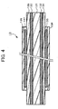
- a flex-rigid wiring board 10 according to an embodiment of the present invention will be described.
- the flex-rigid wiring board 20 includes a first rigid board (rigid board) 11, a second rigid board 12, and a flexible board 13 connecting the rigid boards 11 and 12 to each other.
- any desired circuit pattern is formed on each of the first and second rigid boards 11 and 12, any desired circuit pattern is formed. If required, for example, an electronic component such as a semiconductor chip is connected to each board.
- stripe-shaped wiring 13a is formed for connecting the circuit patterns on the first and second rigid boards 11 and 12.
- the wiring 13a connects the circuit patterns on the rigid boards 11 and 12 to each other.
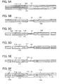
- Fig. 2 is an enlarged sectional view of an area denoted by reference numeral 2 in Fig. 1A .
- the flexible board 13 has a structure in which a substrate 131, conductor layers 132 and 133, insulating layers 134 and 135, shield layers 136 and 137, and cover lays 138 and 139 are laminated.
- the substrate 131 is composed of an insulating flexible sheet, for example, a polyimide sheet having a thickness of 20 to 50 ⁇ m and preferably about 30 ⁇ m.
- the conductor layers 132 and 133 are formed on the front and back surfaces of the substrate 131, respectively, and each have a wiring stripe pattern 13a.
- each of the conductor layers 132 and 133 has a copper pattern having a thickness of about 5 to 15 ⁇ m.
- the insulating layers 134 and 135 are composed of a polyimide film having a thickness of about 5 to 15 ⁇ m and insulate the conductor layers 132 and 133, respectively, from the outside.
- the shield layers 136 and 137 are conductive layers each including, for example, a silver paste cured film and shield the conductor layers 132 and 133 from external electromagnetic noise and shield the emission of electromagnetic noise toward the outside.
- the cover lays 138 and 139 include insulating films of polyimide or the like having a thickness of about 5 to 15 ⁇ m and insulate and protect the whole flexible board 13 form the outside.
- the rigid board 11 includes a laminate of a first insulating layer 111, a non-flexible substrate 112, a second insulating layer 113, and first and second upper insulating layers 114 and 115.
- the non-flexible substrate 112 gives rigidity to the rigid board 11 and is composed of a non-flexible insulating material such as a glass epoxy resin.
- the non-flexible substrate 112 is disposed with a space from the flexible board 13 in a horizontal direction.
- the non-flexible substrate 112 has substantially the same thickness as the flexible board 13, for example, 50 to 150 ⁇ m and preferably about 100 ⁇ m.
- Each of the first and second insulating layers 111 and 113 is formed by curing prepreg and has a thickness of 50 to 100 ⁇ m and preferably about 50 ⁇ m.
- the prepreg preferably contains a resin having a low flow characteristic.
- Such prepreg can be prepared by impregnating a glass cloth with an epoxy resin and then thermally curing the resin to increase the degree of curing.
- the prepreg can also be formed by impregnating a glass cloth with a resin with high viscosity, impregnating a glass cloth with a resin containing an inorganic filler, e.g., a silica filler, or impregnating a glass cloth with a decreased amount of resin.
- a resin with high viscosity impregnating a glass cloth with a resin containing an inorganic filler, e.g., a silica filler, or impregnating a glass cloth with a decreased amount of resin.
- an inorganic filler e.g., a silica filler
- the first and second insulating layers 111 and 113 cover both the front and the back surfaces of the non-flexible substrate 112 and the flexible board 13 to partially expose the flexible board 13.
- the resin of the first and second insulating layers 111 and 113 is polymerized with the resin of the cover lays 138 and 139 on the surfaces of the flexible board 13.
- the non-flexible substrate 112 and the first and second insulating layers 111 and 113 constitute the core of the rigid board 11 to support the rigid board 11 and hold one of the ends of the flexible board 13 to support and fix the flexible board 13.
- the spaces formed by the non-flexible substrate 112, the flexible board 13, and the first and second insulating layers 111 and 1113 are filled with a resin 125.
- the resin 125 seeps from the low-flow prepreg constituting the first and second insulating layer 111 and 113, for example, during manufacture.
- the resin 125 is cured integrally with the first and second insulating layers 111 and 113.
- vias (via holes or contact holes) 116 are formed in a portion opposing connection pads 13b of the wiring 133 of the flexible board 13.
- the shield layer 137 and the cover lay 139 of the flexible board 13 are removed from a portion opposing the vias 116 (a portion in which the connection pads 13b of the conductor layer 13a are formed).
- the vias 116 pass through the insulating layer 135 of the flexible board 13 to expose the connection pads 13b of the conductor layer 133.
- a conductor layer 117 is formed on the inner surface of each of the vias 116 by copper plating or the like.
- the wiring pattern 117 is connected by plating to the connection pads 13b of the conductor layer 113 of the flexible board 13.
- the vias 116 are filled with a resin.
- an extraction pattern 118 is formed on the second insulating layer 113 to be connected to the wiring pattern 117.
- the extraction pattern 118 includes a copper plating layer or the like.
- a copper pattern 124 insulated from other components is formed at an end of the second insulating layer 113, i.e., at a position beyond the boundary between the flexible board 13 and the non-flexible substrate 112. Therefore, heat generated in the rigid board 11 can be effectively radiated.
- the first upper insulating layer 114 is laminated on the second insulating layer 113.
- the first upper insulating layer 114 is formed by curing a material containing an inorganic material, for example, prepreg prepared by impregnating a glass cloth with a resin. This can improve the resistance to dropping impact.
- the vias 116 are filled with the resin seeping from the prepreg.
- the second upper insulating layer 115 is disposed on the first upper insulating layer 114.
- the second upper insulating layer 115 is also formed by curing prepreg including a glass cloth impregnated with a resin.
- first upper vias 119 are formed to be connected to the extraction pattern 118.
- the vias 119 are filled with a conductor 120 such as copper or the like.
- second upper via vias (second upper via) 121 are formed to be connected to the vias 119.
- the vias 121 are filled with a conductor 121 such as copper or the like. Namely, the vias 119 and 121 form field built-up vias.
- a conductor pattern (circuit pattern) 123 is appropriately formed on the second upper insulating layer 115.
- the vias 119 are appropriately connected to the conductor pattern 123.
- connection portion between the rigid board 12 and the flexible board 13 is the same as that of the connection portion between the rigid board I I and the flexible board 13.
- the end of the flexible board 13 is held between the first and second insulating layers 111 and 113 which constitute the core portion of the rigid board 11 and subjected to resin polymerization.
- connection pads 13b of the conductor layer 133 of the flexible board 13 are connected to the conductor pattern 123 of the rigid board 11 through the wiring pattern (copper plating layer) 117 formed in the vias 116 which are formed in the second insulating layer 113 and the insulating layer 135.
- connection portion has high reliability.
- the vias 116 are filled with the resin of the upper insulating layer 114. Since the vias 116 are fixed and supported by the resin in the vias 116, the connection reliability between the vias 116 and the conductor layer 133 is improved.
- the horizontal extension and contraction of the extensible flexible board 13 is suppressed by the core portion of the rigid board 11. Therefore, bending reliability and heat resistance reliability are high. Also, the flexible substrate portion of the flexible board 13 is exposed between the rigid boards 11 and 12, and thus bending stress applied to wiring is small as compared with a case in which the whole is covered with an insulating resin or the like.
- the end portion of the flexible board 13 is held between the first and second insulating layers 111 and 113 of the rigid board 11. Therefore, a change in dimensions of the flexible board 13 has small influence, and a positional error of the connection lands (the vias 116) of the rigid board 11 can be deceased. Thus, the vias 116 having a smaller diameter can be designed.
- the flexible board 13 is not disposed in the rigid boards 11 and 12. Therefore, the same degree of reliability as that of a general rigid board can be maintained.
- a general-purpose plating solution can be used because of the high resistance to a plating solution.
- a flex material is not used in a rigid portion, the same heat resistance as a usual rigid portion can be maintained.
- the flexible board 13 is partially used and effectively disposed, thereby suppressing the manufacturing cost.
- Each of the upper insulating layers 114 and 115 is formed from usual prepreg.
- Usual prepreg is excellent in compatibility between inner layer patterns, and thus insulation deterioration due to the occurrence of voids or the like can be avoided.
- a fine pattern for example, a pattern with L/S of 60/50 or 50/50 ⁇ m, can be realized. This can be achieved with a limitation on material control.
- a general-purpose interlayer material (prepreg) is used as each of the upper insulating layers 114 and 115. Therefore, in the manufacturing process, IVH (Interstitial Via Hole) including the vias 116 can be filled with the resin constituting the upper insulating layers 114 and 115. Thus, a resin exclusively used for filling in holes need not be used.
- a conductor pattern is formed only on the upper surface of each of the rigid boards 11 and 12 for sake of easy understanding.
- the present invention is not limited to this.
- a conductor pattern may be formed on the lower surface of each of the rigid boards 11 and 12.
- vias 141 are formed in the first insulating layer 111 and the insulating layer 134 of the flexible board 13.
- a wiring pattern 142 is formed and connected to an extraction pattern 143 formed on the first insulating layer 111.
- the wiring pattern 142 and the extraction pattern 143 are formed by patterning a copper plating layer.
- third and fourth upper insulating layers 144 and 145 are laminated on the first insulating layer 111.
- Vias 146 and 147 are formed in the third and fourth upper insulating layers 144 and 145, respectively.
- the vias 146 and 147 are filled with conductors 148 and 149, respectively.
- a conductor pattern 150 is formed on the fourth upper insulating layer 145.
- Copper films are formed on both surfaces of the polyimide substrate 131 processed into a predetermined size. Next, the copper films are patterned to form the conductor layers 132 and 133 each having the wiring pattern 13a and the connection pads 13b.
- the insulating films 134 and 135 each including a polyimide layer are formed on the polyimide substrate 131 and the conductor layers 132 and 133, respectively. Furthermore, silver paste is applied except on the end of the flexible board 13, and the applied silver paste is cured to form the shield layers 136 and 137.
- the cover lays 138 and 139 are formed to cover the shield layers 136 and 137 on the front and the back surfaces, respectively.
- the flexible board 13 having the constitution shown in Fig. 4 is completed.
- the shield layers 136 and 137 and the cover lays 138 and 139 are formed avoiding the connection pads 13b.
- the first insulating film 111, the non-flexible substrate 112, and the second insulating layer 113, which constitute the core of the rigid board 11, are aligned.
- Each of the first and second insulating layers 111 and 113 includes, for example, a prepreg having a thickness of 20 to 50 ⁇ m
- the non-flexible substrate 112 includes, for example, a glass epoxy substrate having a thickness of about 100 ⁇ m.
- the thickness of the non-flexible substrate 112 is preferably substantially the same as the thickness of the flexible board 13.
- the space between the non-flexible substrate 112 and the cover lay 139 is filled with the resin 125, and thus the flexible board 13 and the non-flexible substrate 112 can be securely bonded together.
- the resin 125 filled in the space is cured integrally with the insulating layer 113 to fix the peripheries of the vias 116 with the resin 125, thereby improving the reliability of connection between the vias 116 and the conductor layer 133.
- the non-flexible substrate and the first and second insulating layers constituting the core portion of the rigid board 12 are aligned.
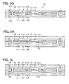
- one of the ends of the flexible board 13 is inserted between the first and second insulating layers 111 and 113 of the rigid board 11 and aligned, and the other end is disposed between the first and second insulating layers and the non-flexible substrate of the rigid board 12. Furthermore, conductor films 161 and 162 are disposed on and below these layers.
- the pressure pressing is performed, for example, using a hydropress apparatus at a temperature of 200°C and a pressure of 40 kgf for a pressure time of about 3 hours.
- the whole is heated to cure the prepreg constituting each of the first and second insulating layers 111 and 113 and the resin 125 to integrate the resins.
- the resin of the cover lays 138 and 139 of the flexible board 13 and the resin of the first and second insulating layers 111 and 113 are polymerized.
- the resin of the insulating layers 111 and 113 is polymerized to fix the peripheries of the vias 116 with the resin, thereby improving the reliability of connection between the vias 116 and the conductor layer 133.
- IVH Interstitial Via Hole 163 is formed by irradiation of CO 2 laser from a CO 2 laser processing apparatus according to demand.
- the vias 116 and 141 are formed for connecting the wiring layers 132 and 133 of the flexible board 13 to the rigid boards 11 and 12.
- Fig. 5D copper plating is conducted on the surfaces of the whole structure.
- the copper plating layers and the copper patterns 161 and 162 previously formed are integrated to form a copper film 171 over the entire surface of the board.
- the copper film 171 is formed in the vias 116 and 141.
- the flexible board 13 is covered with the copper foils 161 and 162 without making direct contact with a plating solution. Therefore, the flexible board 13 is not damaged by the plating solution.
- the copper film 171 on the surface of the board is patterned.
- the wiring patterns 117 and 142 connected to the conductor layers 132 and 133 of the flexible board 13 and the extraction patterns 118 and 143 are formed.
- the copper film 171 is left on the end portions of the first and second insulating layers 111 and 113.
- each of the first and third upper insulating layers 114 and 144 includes, for example, a prepreg prepared by impregnating a glass cloth with a resin.
- the vias 116 and 141 are filled with the resin from the prepreg.
- the resin in the prepreg and the vias is cured by heating to fix the first and third upper insulating layers 114 and 144.
- the vias 119 and 144 are formed in the first and third upper insulating layers 114 and 144, respectively, and filled with a conductor by copper plating or the like.
- the vias 119 and 114 may be filled with conductive paste (e.g., thermosetting resin containing conductive particles) by printing such as screen printing and then subjected to resin curing.
- each of the second and fourth upper insulating layers 115 and 145 includes, for example, usual prepreg prepared by impregnating a glass cloth with a resin.
- the resin of the prepreg is cured by heating to fix the second and fourth upper insulating layers 115 and 145.
- the vias 121 and 147 are formed in the second and fourth upper insulating layers 115 and 145, respectively, and filled with a conductor by copper plating.
- the vias 121 and 147 may be filled with conductive paste (e.g., thermosetting resin containing conductive particles) by printing such as screen printing and then subjected to resin curing.
- conductive paste e.g., thermosetting resin containing conductive particles
- copper foil sheets with resin (resin copper film: RCF) 172 and 173 are disposed on the outermost layers of the board.
- vias 174 and 175 are formed in the RCFs 172 and 173, respectively.
- the vias 174 and 175 are filled with a conductor by copper plating. If required, the surface copper foils are patterned to form conductor patterns.
- the joint portions between the rigid boards 11 and 12 and the flexible board 13 are irradiated with laser beam 158, for example, CO 2 laser, from a laser processing apparatus, using as a stopper the copper foil 171 formed at the ends of the cores of rigid boards 11 and 12 to cut the upper insulating layers 114, 115, 144, and 145, and the copper foil sheets with resin (RCFs) 172 and 173.
- laser beam 158 for example, CO 2 laser
- the energy or irradiation time is controlled so as to cut the copper foil 171 used as a stopper to some extent.
- a structure 181 on the flexible board 13 is separated from the other portions.
- the structure 181 is removed from the flexible board 13 by peeling.
- the copper foils 161 and 162 (refer to Fig. 5B ), which are a base of the remaining copper foil 171, are only pressed by the cover lays 138 and 139 of the flexible board 13 and is not fixed. Similarly, the copper foil 171 is not fixed to the flexible board 13. Therefore, the copper foil 171 is also removed by removal of the structure 181.
- the copper foil 171 is removed from portions not covered with the other members. Therefore, the copper foils 124 and 151 are left on portions covered with the prepregs 113 and 144 at the ends of the first and second insulating layers 111 and 113.
- the flex-rigid wiring board 10 is completed, in which the ends of the flexible board 13 are held between the core portions (the first and second insulating layers 111 and 113) of the rigid boards 11 and 12, and the lands of the rigid bards 11 and 12 are connected to the connection pads of the flexible board by plating.
- plating on the polyimide of the flexible board 13 is not required, thereby securing connection reliability.
- RCF can be used on the outermost layers of the rigid boards 11 and 12. Therefore, the same reliability and dropping resistance as those of a usual rigid board can be secured.
- prepreg including a resin having a low flow property is required for forming the core layer of each of the rigid boards 11 and 13.
- usual prepreg can be used for layers other than the core layers, and thus IVH filling is not required, thereby little producing voids.
- a bending portion includes a flexible board, and thus stability is improved.
- holes are formed in a plurality of layers by laser processing after the formation of outer layers, and thus the manufacturing cost can be suppressed.
- the present invention is not limited to this embodiment.
- the materials, sizes, and number of the layers may be appropriately changed.
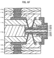
- the vias 116 and 141 may be filled with a conductor such as a plating metal.
- voids are present in the vias 116 and 141.
- the connection reliability of the vias may be degraded due to the expansion of the voids.
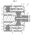
- the vias 116 and 141 are filled with a plating metal as shown in Fig. 7 , with the heat applied, the connection reliability of the vias 116 and 141 can be improved.
- conductor patterns (circuit patterns) 191 and 192 may be formed on the non-flexible substrate 112, for connection with any desired portion.
- conductor patters (circuit patterns) 193 and 194 may be formed on the first and third upper insulating layers 114 and 144, for connection with any desired portion.
- the conductor patters 191, 143, 193, and 150 are connected to each other through the vias 146 and 147 and any other vias.
- the conductor patterns 192, 118,194, and 123 are connected to each other through the vias 119 and 121 and other vias.
- the conductor patterns 123 and 150 are connected to each other through the vias 163.
- the first and second insulating layers 111 and 113 which hold the end of the flexible board 13 therebetween may be composed of RCF.
- Each of the first and third upper insulating layers 114 and 144 and the second and fourth upper insulating layers 115 and 145 may be composed of RCF. In this constitution, a manufacturing step can be omitted.
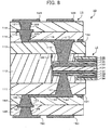
- the flexible board 13 and the non-flexible substrate 112 have substantially the same thickness
- the present invention is not limited to this.
- the flexible board 13 may be thinner than the non-flexible substrate 112.
- the spaces between the flexible board 13, the non-flexible substrate 112, and the firs and second insulating layers 111 and 113 are filled with any resin, for example, the resin seeping from the insulating layers 111 and 113 or a resin previously inserted for adjusting the height during manufacture, In this way, the spaces are filled with the resin 125, and thus the flexible board 13 and the non-flexible substrate 112 can be securely bonded together.
- the resin is integrally cured and fixed by heating during manufacture. Since the resins of the insulating layers 111 and 113 are polymerized, and the resin 125 is integrally cured and fixed, the peripheries of the vias 116 and 141 are fixed with the resin to improve the reliability of connection between the vias 116 and 141 and the conductor layers 133 and 132, respectively.
- the wiring patterns formed on the rigid boards 11 and 12 and the flexible board 13 are not limited to the example shown in Fig. 1 .
- the wiring patterns may be formed in a shape which fans out from the flexible board 13 toward the rigid boards 11 and 12.
- the pitch of wiring 13a of the flexible board 13 may be smaller than that on the connection portion 136.
- many wirings can be disposed on the flexible board 13, and thus a flex-rigid wiring board having high-density wiring can be formed.
- an end of the flexible board 13 is widened to increase the area of a portion to be fixed to each of the rigid boards 11 and 12.
- the strength of the ends of the flexible board 13 can be increased to improve bending resistance
- projections are formed at a position where bending of the flexible board 13 is repeated (for example, the position facing the end surfaces of the rigid boards 11 and 12) to increase the strength of the position where bending is repeated.
- This invention is applicable to a flexible rigid wiring board including a non-flexible substrate portion and a flexible substrate portion.
- the following numbered paragraphs disclose particular feature combinations relating to embodiments of the present disclosure.
Abstract
Description
- The present invention relates to a flexible wiring board partially including a flex board and a method of manufacturing the same.
- Flex-rigid wiring boards each including a rigid portion and a flexible portion are disclosed in, for example, Patent References 1 to 3.
- A flex-rigid wiring board disclosed in Patent Reference 1 includes a core board provided as a rigid portion, a flexible board disposed adjacent to the core board in the horizontal direction, a flexible adhesive layer laminated on the core board and the flexible board, a wiring pattern formed on the flexible adhesive layer disposed in the rigid portion, and blind vias and/or through holes for connecting wiring patterns formed in respective layers.
- In this constitution, the flexible adhesive layer is laminated on the flexible board, and thus bending stress of the flexible board is large. Therefore, large force is applied to a connection portion between a conductor of the flexible board and a conductor of the rigid board, thereby easily causing disconnection.
-
Patent Reference 2 discloses a method of manufacturing a flex-rigid wiring board. In the method, first, a rigid board having a vertical wiring portion formed in a connection region thereof and a flexible board having a connection terminal formed at an end thereof are separately formed. Then, the connection region of the rigid board is cut out to a depth larger than the thickness of the flexible board to form a step. Next, the connection terminal of the flexible board is connected to the vertical wiring portion of the step. - In the manufacturing method, connection between conductors of the rigid board and the flexible board becomes weak.
- A flex-rigid wiring board disclosed in Patent Reference 3 includes a rigid board and a flexible board which are bonded together with an insulating adhesive to form a unified body. Furthermore, connection electrode pads of the rigid board and the flexible board are electrically and physically connected through bulk conductors provided through the insulating adhesive.
- In the flex-rigid wiring board with the above-described constitution, the flexible board is disposed on one of the sides of the rigid substrate, and laser is applied to the flexible board side to form vias for plating connection. In this structure, a bending portion is maintained only on one side, and thus a portion connected by plating has low connection reliability.
- Patent Reference 1: Unexamined Japanese Patent Application KOKAI Publication No.
2006-140213 - Patent Reference 2: Unexamined Japanese Patent Application KOKAI Publication No.
2006-100703 - Patent Reference 3: International Publication No.
WO2004/093508 - The present invention has been achieved in consideration of the above-described situation, and it is an object of she present invention to provide a flex-rigid wiring board with high reliability, particularly high connection reliability, and a method of manufacturing the same.
It is another object of the present invention to provide a flex-rigid wiring board which can be easily manufactured at low cost, and a method of manufacturing the same. - In order to achieve the objects, in a first aspect of the present invention, a flex-rigid wiring board includes
- a flexible substrate having a conductor pattern,
- a non-flexible substrate disposed adjacent to the flexible substrate in the horizontal direction,
- an insulating layer covering the flexible substrate and the non-flexible substrate to expose at least a portion of the flexible substrate,
- and a conductor pattern formed on the insulating layer,
- the conductor pattern of the flexible substrate being connected by plating to the conductor pattern on the insulating layer.
- In order to achieve the objects, in a second aspect of the present invention, a flex-rigid wiring board includes
- a flexible substrate having a conductor pattern,
- a non-flexible substrate disposed adjacent to the flexible substrate in the horizontal direction,
- and an insulating layer covering the flexible substrate and the non-flexible substrate to expose at least a portion of the flexible substrate,
- wherein vias are formed in the insulating layer,
- a conductor pattern is formed on the insulating layer, and the conductor pattern on the insulating layer is connected to the conductor pattern on the flexible substrate through the vias.
- In order to achieve the objects, in a third aspect of the present invention, a flex-rigid wiring board includes
- a flexible substrate having a conductor pattern and a protective layer covering the conductor pattern,
- a non-flexible substrate disposed adjacent to the flexible substrate in the horizontal direction,
- an insulating layer covering the flexible substrate and the non-flexible substrate to expose at least a portion of the flexible substrate,
- and a conductor pattern formed on the insulating layer,
- In order to achieve the objects, in a fourth aspect of the present invention, a method of manufacturing a flex-rigid wiring board includes
- disposing a flexible substrate having a conductor pattern and a non-flexible substrate adjacent to each other,
- covering the boundary between the flexible substrate and the non-flexible substrate with an insulating layer having a conductor pattern,
- forming vias which pass through the insulating layer and reach the conductor pattern of the flexible substrate,
- and connecting by plating the conductor pattern of the flexible substrate to the conductor pattern on the insulating layer through the vias.
- According to the invention, an insulating layer covers a flexible substrate, thereby defining a conductor pattern of the flexible substrate and a conductor pattern on the insulating layer. Therefore, high connection reliability between the conductor pattern of the flexible substrate and the conductor pattern on the insulating layer can be achieved.
-
- [
Fig. 1A] Fig. 1A is a side view of a flex-rigid wiring board according to an embodiment of the present invention. - [
Fig. 1B] Fig. 1B is a plan view of a flex-rigid wiring board according to an embodiment of the present invention. - [
Fig. 2] Fig. 2 is a partially enlarged view ofFig. 1A . - [
Fig. 3] Fig. 3 is a view showing a modified example of the flex-rigid wiring board shown inFig. 2 . - [
Fig. 4] Fig. 4 is a side view of a flexible board. - [
Fig. 5A] Fig. 5A is a view illustrating steps of a method of manufacturing a flex-rigid wiring board according to an embodiment of the invention. - [
Fig. 5B] Fig. 5B is a view illustrating steps of a method of manufacturing a flex-rigid wiring board according to an embodiment of the invention. - [
Fig. 5C] Fig. 5C is a view illustrating steps of a method of manufacturing a flex-rigid wiring board according to an embodiment of the invention. - [
Fig. 5D] Fig. 5D is a view illustrating steps of a method of manufacturing a flex-rigid wiring board according to an embodiment of the invention. - [
Fig. 5E] Fig. 5E is a view illustrating steps of a method of manufacturing a flex-rigid wiring board according to an embodiment of the invention. - [
Fig. 5F] Fig. 5F is a view illustrating steps of a method of manufacturing a flex-rigid wiring board according to an embodiment of the invention. - [
Fig. 5G] Fig. 5G is a view illustrating steps of a method of manufacturing a flex-rigid wiring board according to an embodiment of the invention. - [
Fig. 5H] Fig. 5H is a view illustrating steps of a method of manufacturing a flex-rigid wiring board according to an embodiment of the invention. - [
Fig. 5I] Fig. 5I is a view illustrating steps of a method of manufacturing a flex-rigid wiring board according to an embodiment of the invention. - [
Fig. 5J] Fig. 5J is a view illustrating steps of a method of manufacturing a flex-rigid wiring board according to an embodiment of the invention. - [
Fig. 5K] Fig. 5K is a view illustrating steps of a method of manufacturing a flex-rigid wiring board according to an embodiment of the invention. - [
Fig. 5L] Fig. 5L is a view illustrating steps of a method of manufacturing a flex-rigid wiring board according to an embodiment of the invention. - [
Fig. 6A] Fig. 6A is an enlarged view illustrating the method of manufacturing a flex-rigid wiring board shown inFigs. 5A to 5L . - [
Fig. 6B] Fig. 6B is an enlarged view illustrating the method of manufacturing a flex-rigid wiring board shown inFigs. 5A to 5L . - [
Fig. 6C] Fig. 6C is an enlarged view illustrating the method of manufacturing a flex-rigid wiring board shown inFigs. 5A to 5L . - [
Fig. 6D] Fig. 6D is an enlarged view illustrating the method of manufacturing a flex-rigid wiring board shown inFigs. 5A to 5L . - [
Fig. 6E] Fig. 6E is an enlarged view illustrating the method of manufacturing a flex-rigid wiring board shown inFigs. 5A to 5L . - [
Fig. 6F] Fig. 6F is an enlarged view illustrating the method of manufacturing a flex-rigid wiring board shown inFigs. 5A to 5L . - [
Fig. 7] Fig. 7 is a view showing a modified example of the flex-rigid wiring board shown inFig. 2 . - [
Fig. 8] Fig. 8 is a view showing a modified example of the flex-rigid wiring board shown inFig. 2 . - [
Fig. 9] Fig. 9 is a view showing an example of fan-out of a wiring pattern. - [
Fig. 10] Fig. 10 is a view showing an example in which a flexible substrate is partially widened to increase strength. - [
Fig. 11] Fig. 11 is a view showing an example in which a flexible substrate is partially widened to increase strength. -
- 11, 12
- rigid board
- 13
- flexible board
- 131
- substrate
- 132, 133
- conductor layer
- 134, 135
- insulating layer
- 136, 137
- shield layer
- 138, 139
- cover lay
- 111, 113
- insulating layer
- 112
- non-flexible substrate
- 114, 115, 144, 145
- upper insulating layer
- 116, 119, 121, 141, 146, 147
- via
- 117,142
- wiring pattern
- 118, 143
- extraction pattern
- 120, 122
- conductor
- 125
- resin
- A flex-
rigid wiring board 10 according to an embodiment of the present invention will be described. - As shown in
Figs. 1A and 1B , the flex-rigid wiring board 20 according to this embodiment includes a first rigid board (rigid board) 11, a secondrigid board 12, and aflexible board 13 connecting therigid boards - On each of the first and second
rigid boards - On the
flexible board 13, stripe-shapedwiring 13a is formed for connecting the circuit patterns on the first and secondrigid boards wiring 13a connects the circuit patterns on therigid boards - Next, with respect to the structure of the junction portions between the
rigid boards flexible board 13, the junction portion between therigid board 11 and theflexible board 13 will be described as an example with reference toFig. 2. Fig. 2 is an enlarged sectional view of an area denoted byreference numeral 2 inFig. 1A . - As shown in the drawing, the
flexible board 13 has a structure in which asubstrate 131, conductor layers 132 and 133, insulatinglayers - The
substrate 131 is composed of an insulating flexible sheet, for example, a polyimide sheet having a thickness of 20 to 50 µm and preferably about 30 µm. - The conductor layers 132 and 133 are formed on the front and back surfaces of the
substrate 131, respectively, and each have awiring stripe pattern 13a. For example, each of the conductor layers 132 and 133 has a copper pattern having a thickness of about 5 to 15 µm. - The insulating
layers - The shield layers 136 and 137 are conductive layers each including, for example, a silver paste cured film and shield the conductor layers 132 and 133 from external electromagnetic noise and shield the emission of electromagnetic noise toward the outside.
- The cover lays 138 and 139 include insulating films of polyimide or the like having a thickness of about 5 to 15 µm and insulate and protect the whole
flexible board 13 form the outside. - On the other hand, the
rigid board 11 includes a laminate of a first insulatinglayer 111, anon-flexible substrate 112, a second insulatinglayer 113, and first and second upper insulatinglayers - The
non-flexible substrate 112 gives rigidity to therigid board 11 and is composed of a non-flexible insulating material such as a glass epoxy resin. Thenon-flexible substrate 112 is disposed with a space from theflexible board 13 in a horizontal direction. Thenon-flexible substrate 112 has substantially the same thickness as theflexible board 13, for example, 50 to 150 µm and preferably about 100 µm. - Each of the first and second insulating
layers - The prepreg preferably contains a resin having a low flow characteristic. Such prepreg can be prepared by impregnating a glass cloth with an epoxy resin and then thermally curing the resin to increase the degree of curing.
- The prepreg can also be formed by impregnating a glass cloth with a resin with high viscosity, impregnating a glass cloth with a resin containing an inorganic filler, e.g., a silica filler, or impregnating a glass cloth with a decreased amount of resin.
- The first and second insulating
layers non-flexible substrate 112 and theflexible board 13 to partially expose theflexible board 13. The resin of the first and second insulatinglayers flexible board 13. - The
non-flexible substrate 112 and the first and second insulatinglayers rigid board 11 to support therigid board 11 and hold one of the ends of theflexible board 13 to support and fix theflexible board 13. - The spaces formed by the
non-flexible substrate 112, theflexible board 13, and the first and second insulatinglayers 111 and 1113 are filled with aresin 125. Theresin 125 seeps from the low-flow prepreg constituting the first and second insulatinglayer resin 125 is cured integrally with the first and second insulatinglayers - Furthermore, in the second insulating
layer 113, vias (via holes or contact holes) 116 are formed in a portion opposingconnection pads 13b of thewiring 133 of theflexible board 13. - In the
flexible board 13, theshield layer 137 and the cover lay 139 of theflexible board 13 are removed from a portion opposing the vias 116 (a portion in which theconnection pads 13b of theconductor layer 13a are formed). Thevias 116 pass through the insulatinglayer 135 of theflexible board 13 to expose theconnection pads 13b of theconductor layer 133. - In addition, a
conductor layer 117 is formed on the inner surface of each of thevias 116 by copper plating or the like. Thewiring pattern 117 is connected by plating to theconnection pads 13b of theconductor layer 113 of theflexible board 13. Thevias 116 are filled with a resin. - Furthermore, an
extraction pattern 118 is formed on the second insulatinglayer 113 to be connected to thewiring pattern 117. Theextraction pattern 118 includes a copper plating layer or the like. - Furthermore, a
copper pattern 124 insulated from other components is formed at an end of the second insulatinglayer 113, i.e., at a position beyond the boundary between theflexible board 13 and thenon-flexible substrate 112. Therefore, heat generated in therigid board 11 can be effectively radiated. - The first upper insulating
layer 114 is laminated on the second insulatinglayer 113. The first upper insulatinglayer 114 is formed by curing a material containing an inorganic material, for example, prepreg prepared by impregnating a glass cloth with a resin. This can improve the resistance to dropping impact. In the process of manufacturing the flex-rigid wiring board, thevias 116 are filled with the resin seeping from the prepreg. - Furthermore, the second upper insulating
layer 115 is disposed on the first upper insulatinglayer 114. The second upper insulatinglayer 115 is also formed by curing prepreg including a glass cloth impregnated with a resin. - In the first upper insulating
layer 114 disposed on the second insulatinglayer 113, vias (first upper vias) 119 are formed to be connected to theextraction pattern 118. Thevias 119 are filled with aconductor 120 such as copper or the like. In the second upper insulatinglayer 115 laminated on the first upper insulatinglayer 114, vias (second upper via) 121 are formed to be connected to thevias 119. Thevias 121 are filled with aconductor 121 such as copper or the like. Namely, thevias - Furthermore, a conductor pattern (circuit pattern) 123 is appropriately formed on the second upper insulating
layer 115. Thevias 119 are appropriately connected to theconductor pattern 123. - The constitution of the connection portion between the
rigid board 12 and theflexible board 13 is the same as that of the connection portion between the rigid board I I and theflexible board 13. - In the flex-
rigid wiring board 10 having the above constitution, the end of theflexible board 13 is held between the first and second insulatinglayers rigid board 11 and subjected to resin polymerization. - Furthermore, the
connection pads 13b of theconductor layer 133 of theflexible board 13 are connected to theconductor pattern 123 of therigid board 11 through the wiring pattern (copper plating layer) 117 formed in thevias 116 which are formed in the second insulatinglayer 113 and the insulatinglayer 135. - Therefore, when the
flexible board 13 is bent, stress applied to theflexible board 13 is not transmitted to the connection portion (thevias 116 and the wiring layer pattern 117) of therigid board 11. Thus, stress applied to the connection portion between therigid board 11 and theflexible board 13 is decreased to improve reliability. - The
conductor layer 133 of theflexible board 13 is connected by plating to thewiring pattern 117 in thevias 116 of therigid board 11. Therefore, the connection portion has high reliability. - The
vias 116 are filled with the resin of the upper insulatinglayer 114. Since thevias 116 are fixed and supported by the resin in thevias 116, the connection reliability between thevias 116 and theconductor layer 133 is improved. - The end surfaces of the insulating
layers flexible board 13 project beyond the end of the upper insulatinglayer 114 which faces theflexible board 13. Therefore, when theflexible board 13 is bent, stress applied to theflexible board 13 is not transmitted to the connection portion (thevias 116 and the wiring pattern 117) of therigid board 11. Thus, stress applied to the connection portion between therigid board 11 and theflexible board 13 is decreased to improve reliability. - The horizontal extension and contraction of the extensible
flexible board 13 is suppressed by the core portion of therigid board 11. Therefore, bending reliability and heat resistance reliability are high. Also, the flexible substrate portion of theflexible board 13 is exposed between therigid boards - In the flex-
rigid wiring board 10, the end portion of theflexible board 13 is held between the first and second insulatinglayers rigid board 11. Therefore, a change in dimensions of theflexible board 13 has small influence, and a positional error of the connection lands (the vias 116) of therigid board 11 can be deceased. Thus, thevias 116 having a smaller diameter can be designed. - The
flexible board 13 is not disposed in therigid boards - Furthermore, the
flexible board 13 is partially used and effectively disposed, thereby suppressing the manufacturing cost. - Each of the upper insulating
layers - Furthermore, a general-purpose interlayer material (prepreg) is used as each of the upper insulating
layers vias 116 can be filled with the resin constituting the upper insulatinglayers - Since a glass epoxy substrate is used as the core portion of each of the
rigid boards - In this embodiment, a conductor pattern is formed only on the upper surface of each of the
rigid boards Fig. 3 , a conductor pattern may be formed on the lower surface of each of therigid boards - In the constitution shown in
Fig. 3 , vias 141 are formed in the first insulatinglayer 111 and the insulatinglayer 134 of theflexible board 13. In each via 141, awiring pattern 142 is formed and connected to anextraction pattern 143 formed on the first insulatinglayer 111. Thewiring pattern 142 and theextraction pattern 143 are formed by patterning a copper plating layer. - Furthermore, third and fourth upper insulating
layers layer 111.Vias layers vias conductors conductor pattern 150 is formed on the fourth upper insulatinglayer 145. - Next, a method of manufacturing the flex-
rigid wiring board 10 having the above-descried construction will be described. - First, a method for manufacturing the
flexible board 13 will be described. - Copper films are formed on both surfaces of the
polyimide substrate 131 processed into a predetermined size. Next, the copper films are patterned to form the conductor layers 132 and 133 each having thewiring pattern 13a and theconnection pads 13b. - The insulating
films polyimide substrate 131 and the conductor layers 132 and 133, respectively. Furthermore, silver paste is applied except on the end of theflexible board 13, and the applied silver paste is cured to form the shield layers 136 and 137. - Then, the cover lays 138 and 139 are formed to cover the shield layers 136 and 137 on the front and the back surfaces, respectively.
- As a result, the
flexible board 13 having the constitution shown inFig. 4 is completed. The shield layers 136 and 137 and the cover lays 138 and 139 are formed avoiding theconnection pads 13b. - Next, a method of bonding the
rigid boards flexible board 13 together will be described. - First, as shown in
Fig. 5A , the first insulatingfilm 111, thenon-flexible substrate 112, and the second insulatinglayer 113, which constitute the core of therigid board 11, are aligned. Each of the first and second insulatinglayers non-flexible substrate 112 includes, for example, a glass epoxy substrate having a thickness of about 100 µm. - As shown in
Fig. 2 , the thickness of thenon-flexible substrate 112 is preferably substantially the same as the thickness of theflexible board 13. In this case, the space between thenon-flexible substrate 112 and the cover lay 139 is filled with theresin 125, and thus theflexible board 13 and thenon-flexible substrate 112 can be securely bonded together. - The
resin 125 filled in the space is cured integrally with the insulatinglayer 113 to fix the peripheries of thevias 116 with theresin 125, thereby improving the reliability of connection between thevias 116 and theconductor layer 133. - Similarly, the non-flexible substrate and the first and second insulating layers constituting the core portion of the
rigid board 12 are aligned. - Furthermore, one of the ends of the
flexible board 13 is inserted between the first and second insulatinglayers rigid board 11 and aligned, and the other end is disposed between the first and second insulating layers and the non-flexible substrate of therigid board 12. Furthermore,conductor films - Next, as shown in
Fig. 5B , these layers are pressed under pressure. At this time, as shown in an enlarged view ofFig. 6A , the spaces between thenon-flexible substrate 112 and theflexible board 13 are filled with theresin 125 extruded from the prepreg constituting each of the first and second insulatinglayers resin 125, theflexible board 13 and thenon-flexible substrate 112 can be securely bonded together. - The pressure pressing is performed, for example, using a hydropress apparatus at a temperature of 200°C and a pressure of 40 kgf for a pressure time of about 3 hours.
- Then, the whole is heated to cure the prepreg constituting each of the first and second insulating
layers resin 125 to integrate the resins. At the same time, the resin of the cover lays 138 and 139 of theflexible board 13 and the resin of the first and second insulatinglayers layers vias 116 with the resin, thereby improving the reliability of connection between thevias 116 and theconductor layer 133. - Next, as shown in
Fig. 5C , IVH (Interstitial Via Hole) 163 is formed by irradiation of CO2 laser from a CO2 laser processing apparatus according to demand. At the same time, as shown in an enlarged view ofFig. 6B , thevias flexible board 13 to therigid boards - Then, as shown in
Fig. 5D , copper plating is conducted on the surfaces of the whole structure. The copper plating layers and thecopper patterns copper film 171 over the entire surface of the board. As shown inFig. 6C , thecopper film 171 is formed in thevias flexible board 13 is covered with the copper foils 161 and 162 without making direct contact with a plating solution. Therefore, theflexible board 13 is not damaged by the plating solution. - Then, as shown in
Fig. 5E , thecopper film 171 on the surface of the board is patterned. In this step, thewiring patterns flexible board 13 and theextraction patterns Fig. 6D , thecopper film 171 is left on the end portions of the first and second insulatinglayers - Then, as shown in
Fig. 5F , the first and third upper insulatinglayers layers vias - Then, the resin in the prepreg and the vias is cured by heating to fix the first and third upper insulating
layers vias layers vias - Then, as shown in
Fig. 5G , the second and fourth upper insulatinglayers layers - Next, the resin of the prepreg is cured by heating to fix the second and fourth upper insulating
layers - Furthermore, the
vias layers vias vias vias - If required, as shown in
Fig. 5H , copper foil sheets with resin (resin copper film: RCF) 172 and 173 are disposed on the outermost layers of the board. - Then, the whole is heated to cure the resin.
- Next, as shown in
Fig. 5I , vias 174 and 175 are formed in theRCFs vias 174 and 175 are filled with a conductor by copper plating. If required, the surface copper foils are patterned to form conductor patterns. - Next, as shown in
Figs. 5J and6E , the joint portions between therigid boards flexible board 13 are irradiated withlaser beam 158, for example, CO2 laser, from a laser processing apparatus, using as a stopper thecopper foil 171 formed at the ends of the cores ofrigid boards layers copper foil 171 used as a stopper to some extent. - As a result, as shown in
Fig. 5H , astructure 181 on theflexible board 13 is separated from the other portions. - Then, as shown in
Fig. 5L , thestructure 181 is removed from theflexible board 13 by peeling. The copper foils 161 and 162 (refer toFig. 5B ), which are a base of the remainingcopper foil 171, are only pressed by the cover lays 138 and 139 of theflexible board 13 and is not fixed. Similarly, thecopper foil 171 is not fixed to theflexible board 13. Therefore, thecopper foil 171 is also removed by removal of thestructure 181. - Consequently, the
copper foil 171 is removed from portions not covered with the other members. Therefore, the copper foils 124 and 151 are left on portions covered with theprepregs layers - As a result, the flex-
rigid wiring board 10 is completed, in which the ends of theflexible board 13 are held between the core portions (the first and second insulatinglayers 111 and 113) of therigid boards rigid bards - In the above-described constitution, plating on the polyimide of the
flexible board 13 is not required, thereby securing connection reliability.
In addition, RCF can be used on the outermost layers of therigid boards - In the manufacturing method, prepreg including a resin having a low flow property is required for forming the core layer of each of the
rigid boards - Furthermore, only a bending portion includes a flexible board, and thus stability is improved.
- Furthermore, holes are formed in a plurality of layers by laser processing after the formation of outer layers, and thus the manufacturing cost can be suppressed.
- Since holes are formed in a plurality of layers by laser processing after the formation of outer layers, opening accuracy of the flexible board is increased.
- Since a glass epoxy substrate is used for the core portions of the
rigid boards - Although the flex-
rigid wiring board 10 according to an embodiment of the present invention is descried above, the present invention is not limited to this embodiment. - For example, the materials, sizes, and number of the layers may be appropriately changed.
- As illustrated in
Fig. 7 , thevias vias vias rigid wiring board 10, the connection reliability of the vias may be degraded due to the expansion of the voids. When thevias Fig. 7 , with the heat applied, the connection reliability of thevias - Similarly, conductor patterns (circuit patterns) 191 and 192 may be formed on the
non-flexible substrate 112, for connection with any desired portion. - Also, conductor patters (circuit patterns) 193 and 194 may be formed on the first and third upper insulating
layers - The conductor patters 191, 143, 193, and 150 are connected to each other through the
vias conductor patterns 192, 118,194, and 123 are connected to each other through thevias conductor patterns vias 163. - The first and second insulating
layers flexible board 13 therebetween may be composed of RCF. Each of the first and third upper insulatinglayers layers - Although, in this embodiment, the
flexible board 13 and thenon-flexible substrate 112 have substantially the same thickness, the present invention is not limited to this. For example, as shown inFig. 8 , theflexible board 13 may be thinner than thenon-flexible substrate 112. In this case, the spaces between theflexible board 13, thenon-flexible substrate 112, and the firs and second insulatinglayers layers resin 125, and thus theflexible board 13 and thenon-flexible substrate 112 can be securely bonded together. - The resin is integrally cured and fixed by heating during manufacture. Since the resins of the insulating
layers resin 125 is integrally cured and fixed, the peripheries of thevias vias - In addition, the wiring patterns formed on the
rigid boards flexible board 13 are not limited to the example shown inFig. 1 . For example, as illustrated inFig. 9 , the wiring patterns may be formed in a shape which fans out from theflexible board 13 toward therigid boards wiring 13a of theflexible board 13 may be smaller than that on theconnection portion 136. In this case, many wirings can be disposed on theflexible board 13, and thus a flex-rigid wiring board having high-density wiring can be formed. - In order to increase the strength of the boundary portions between the
rigid boards flexible board 13, as illustrated inFigs. 10 and 11 , it is effective to partially widen theflexible board 13. In this case, the area of connection between theflexible board 13 and therigid boards - In an example shown in
Fig. 10 , an end of theflexible board 13 is widened to increase the area of a portion to be fixed to each of therigid boards flexible board 13 can be increased to improve bending resistance, - In an example shown in
Fig. 11 , projections are formed at a position where bending of theflexible board 13 is repeated (for example, the position facing the end surfaces of therigid boards 11 and 12) to increase the strength of the position where bending is repeated. - This invention is applicable to a flexible rigid wiring board including a non-flexible substrate portion and a flexible substrate portion.
The following numbered paragraphs disclose particular feature combinations relating to embodiments of the present disclosure. - 1. A flex-rigid wiring board comprising:
- a flexible substrate having a conductor pattern;
- a non-flexible substrate disposed adjacent to the flexible substrate in the horizontal direction;
- an insulating layer covering the flexible substrate and the non-flexible substrate to expose at least a portion of the flexible substrate; and
- a conductor pattern formed on the insulating layer; wherein the conductor pattern of the flexible substrate is connected by plating to the conductor pattern on the insulating layer.
- 2. The flex-rigid wiring board according to paragraph 1, wherein the flexible substrate and the non-flexible substrate are disposed with a space therebetween, and the space is filled with a resin.
- 3. The flex-rigid wiring board according to paragraph 1, wherein the flexible substrate and the non-flexible substrate are disposed with a space therebetween, the space is filled with a resin,
and the resin is cured integrally with the insulating layer. - 4. The flex-rigid wiring board according to paragraph 1, further comprising
a conductor pattern formed on the surface of the non-flexible substrate. - 5. The flex-rigid wiring board according to paragraph 1, wherein the insulating layer covers both the front and back surfaces of the boundary region between the ends of the flexible substrate and the non-flexible substrate.
- 6. The flex-rigid wiring board according to paragraph 1, wherein the insulating layer covers both the front and back surfaces of the boundary region between the ends of the flexible substrate and the non-flexible substrate,
a via is formed in the insulating layer,
and the conductor pattern on the insulating layer is connected to the conductor pattern on the non-flexible substrate through the via. - 7. The flex-rigid wiring board according to paragraph 1, further comprising:
- an upper insulating layer formed on the insulating layer; and
- an upper layer conductor pattern formed on the upper insulating layer; wherein the conductor pattern on the insulating layer is connected to the upper layer conductor pattern through an upper layer via filled with a plating metal, and the upper insulating layer includes a cured resin layer containing an inorganic material.
- 8. The flex-rigid wiring board according to paragraph 1, further comprising:
- a first upper insulating layer formed on the insulating layer;
- a first upper conductor pattern formed on the first upper insulating layer;
- a second upper insulating layer formed on the first upper conductor pattern; and
- a second upper conductor pattern formed on the second upper insulating layer; wherein the conductor pattern on the insulating layer is connected to the first upper conductor layer through a first upper via filled with a plating metal; and
- the first and second upper conductor patterns are connected through a second upper via filled with a plating metal and formed in a portion substantially directly above the first upper via of the second upper insulating layer.
- 9. The flex-rigid wiring board according to paragraph 1, further comprising:
- an upper insulating layer formed on the insulating layer;
- an upper layer via formed in the upper insulating layer and connected to the conductor pattern on the insulating layer; and
- a conductor pattern formed on the upper insulating layer and connected to the upper layer via.
- 10. The flex-rigid wiring board according to paragraph 1, wherein the upper insulating layer includes a glass cloth.
- 11. The flex-rigid wiring board according to paragraph 1, further comprising
a copper foil sheet with resin laminated on the insulating layer, the copper foil sheet with resin being cured. - 12. A flex-rigid wiring board comprising:
- a flexible substrate having a conductor pattern;
- a non-flexible substrate disposed adjacent to the flexible substrate in the horizontal direction; and
- an insulating layer covering the flexible substrate and the non-flexible substrate to expose at least a portion of the flexible substrate; wherein a via is formed in the insulating layer,
- a conductor pattern is formed on the insulating layer,
- and the conductor pattern on the insulating layer is connected to the conductor pattern on the flexible substrate through the via.
- 13. The flex-rigid wiring board according to
paragraph 12, further comprising:- an upper insulating layer formed on the insulating layer; and
- an upper layer conductor pattern formed on the upper insulating layer; wherein the conductor pattern on the insulating layer is connected to the upper layer conductor pattern through an upper layer via formed in the upper insulating layer and filled with a plating metal.
- 14. The flex-rigid wiring board according to
paragraph 12, further comprising
a resin layer containing a resin and disposed on the insulating layer, wherein the via is filled with the resin of the resin layer. - 15. The flex-rigid wiring board according to
paragraph 12, wherein the via is filled with a metal. - 16. The flex-rigid wiring board according to
paragraph 12, wherein the via passes through the insulating layer and is filled with a plating metal,
an upper insulating layer and an upper conductor pattern are laminated on the insulating layer,
the conductor pattern formed on the insulating layer is connected to the upper conductor pattern through an upper layer via formed in the upper insulating layer,
and the upper layer via is connected to the via filled with the plating metal. - 17. The flex-rigid wiring board according to
paragraph 12, wherein the conductor pattern on the insulating layer extends to the end of the insulating layer beyond the boundary between the flexible substrate and the non-flexible substrate. - 18. The flex-rigid wiring board according to
paragraph 12, further comprising
a planar conductor layer formed at the end of the insulating layer on the side facing the flexible substrate. - 19. The flex-rigid wiring board according to
paragraph 12, wherein the flexible substrate has a plurality of connection pads to be connected to vias,
the pitch of the connection pads is larger than the pitch of a plurality of conductor patterns formed on the flexible substrate,
and the conductor patterns are formed so that the pitch increases toward the connection pads and electrically connected to the corresponding connection pads. - 20. The flex-rigid wiring board according to
paragraph 12, further comprising:- an upper insulating layer formed on the insulating layer; and
- an upper layer conductor pattern formed on the upper insulating layer; wherein the conductor pattern on the insulating layer is connected to the upper layer conductor pattern through an upper layer via formed in the upper insulating layer; and
- the end of the insulating layer, which faces the flexible substrate, projects beyond the end of the upper insulating layer, which faces the flexible substrate.
- 21. The flex-rigid wiring board according to
paragraph 12, further comprising: an upper insulating layer formed on the insulating layer; and
an upper layer conductor pattern formed on the upper insulating layer; wherein the conductor pattern on the insulating layer is connected to the upper layer conductor pattern through an upper layer via formed in the upper insulating layer; and
the upper layer via is filled with a cured product of a conductive paste. - 22. A flex-rigid wiring board comprising:
- a flexible substrate having a conductor pattern and a protective layer covering the conductor pattern;
- a non-flexible substrate disposed adjacent to the flexible substrate in the horizontal direction;
- an insulating layer covering the flexible substrate and the non-flexible substrate to expose at least a portion of the flexible substrate; and
- a conductor pattern formed on the insulating layer; wherein
- the conductor pattern on the flexible substrate is connected by plating to the conductor pattern on the insulating layer through a via formed in the insulating layer.
- 23. The flex-rigid wiring board according to paragraph 22, wherein an insulating layer is formed between the conductor pattern and the protective layer,
the via is formed to pass through the insulating layer,
the protective layer is provided in a region without the via, and
a space between the non-flexible substrate and the protective layer and in the periphery of the via is filled with a resin. - 24. The flex-rigid wiring board according to paragraph 22, wherein the protective layer is provided in a region without the via,
the flexible substrate including the protective layer is thinner than the non-flexible substrate, and
a space between the protective layer and the insulating layer and in the periphery of the via is filled with a resin, the resin being cured integrally with the insulating layer. - 25. The flex-rigid wiring board according to paragraph 22, wherein the flexible substrate includes a conductor pattern and at least one protective layer covering the conductor pattern, the thickness of the flexible substrate including the protective layer is substantially the same as that of the non-flexible substrate,
the protective layer is provided in a region without the via, and
a space between the non-flexible substrate and the protective layer and in the periphery of the via is filled with a resin. - 26. The flex-rigid wiring board according to paragraph 22, wherein the flexible substrate includes a conductor pattern and a protective layer covering the conductor pattern,
the thickness of the flexible substrate including the protective layer is substantially the same as that of the non-flexible substrate, the protective layer is provided in a region without the via, and
a space between the non-flexible substrate and the protective layer and in the periphery of the via is filled with a resin, the resin being cured integrally with the insulating layer. - 27. The flex-rigid wiring board according to paragraph 22, wherein the flexible substrate is thinner than the non-flexible substrate.
- 28. The flex-rigid wiring board according to paragraph 22, wherein in the flexible substrate, a portion where the resins of the flexible substrate and the insulating layer are polymerized is wider than a portion where the resins are not polymerized.
- 29. The flex-rigid wiring board according to paragraph 22, wherein in the flexible substrate, the boundary portion between the flexible substrate and the insulating layer is wider than other portions.
- 30. The flex-rigid wiring board according to paragraph 22, wherein the protective layer includes an insulating film, and a via is formed in the insulating layer and the insulating film to pass through them, for electrically connecting the conductor pattern on the insulating layer to the conductor pattern formed on the flexible substrate.
- 31. The flex-rigid wiring board according to paragraph 22, wherein the protective layer of the flexible substrate includes a shield layer against an electromagnetic wave.
- 32. The flex-rigid wiring board according to paragraph 22, further comprising:
- a conductor pattern formed on the flexible substrate;
- an insulating film formed on the conductor pattern; and
- an electromagnetic shield layer formed on the insulating film.
- 33. The flex-rigid wiring board according to paragraph 22, further comprising:
- a conductor pattern formed on the flexible substrate;
- an insulating film formed on the conductor pattern;
- an electromagnetic shield layer formed on the insulating film; and
- a protective layer formed on the electromagnetic shield layer.
- 34. The flex-rigid wiring board according to paragraph 22, further comprising:
- a conductor pattern formed on the flexible substrate;
- an insulating film formed on the conductor pattern;
- an electromagnetic shield layer formed on the insulating film; and
- a protective layer formed on the electromagnetic shield layer to make contact with the insulating layer.
- 35. A method of manufacturing a flex-rigid wiring board comprising:
- disposing a flexible substrate having a conductor pattern and a non-flexible substrate adjacent to each other;
- covering the boundary between the flexible substrate and the non-flexible substrate with an insulating layer having a conductor pattern; forming a via which passes through the insulating layer and reaches the conductor pattern of the flexible substrate; and
- connecting by plating the conductor pattern of the flexible substrate to the conductor pattern on the insulating layer through the via.
- 36. The method according to paragraph 35,
wherein the insulating layer contains a resin,
a space between the non-flexible substrate, the flexible substrate, and the insulating layer is filled with the resin of the insulating layer, and
the filled resin is cured integrally with the insulating layer. - 37. The method according to paragraph 35,
wherein the via is filled with a plating metal by the plating. - 38. The method according to paragraph 35,
wherein the insulating layer covers the front and back surfaces of the boundary between the flexible substrate and the non-flexible substrate. - 39. The method according to paragraph 35, further comprising:
- disposing a metal foil on the insulating layer and the flexible substrate;
- disposing a second insulating layer on the metal foil; and
- cutting the second insulating layer at a position corresponding to the end of the insulating layer by the laser using the metal foil as a stopper.
- 40. The method according to paragraph 35, further comprising:
- disposing a metal foil on the insulating layer and the flexible substrate;
- disposing a second insulating layer on the metal foil;
- cutting the second insulating layer at a position corresponding to the end of the insulating layer by the laser using the metal foil as a stopper; and
- removing a portion remaining on the flexible substrate after the laser cutting together with the metal foil.
- 41. The method according to paragraph 35, further comprising:
- disposing a metal foil on the insulating layer and the flexible substrate;
- patterning the metal foil to form a circuit pattern on the insulating layer;
- disposing a second insulating layer on the metal foil; and
- cutting the second insulating layer by the laser at a position corresponding to the end of the insulating layer using the metal foil as a stopper.
- 42. The method according to paragraph 35, further comprising:
- disposing a metal foil on the insulating layer and the flexible substrate;
- disposing a second insulating layer on the metal foil;
- forming a conductor pattern on the second insulating layer; and
- cutting the second insulating layer by the laser at a position corresponding to the end of the insulating layer using the metal foil as a stopper.
- 43. The method according to paragraph 35, wherein the second insulating layer contains a resin, and the via is filled with the resin of the second insulating layer.
Claims (8)
- A method of manufacturing a flex-rigid wiring board comprising:disposing a flexible substrate having a conductor pattern and a non-flexible substrate adjacent to each other;covering the boundary between the flexible substrate and the non-flexible substrate with an insulating layer having a conductor pattern;forming a via which passes through the insulating layer and reaches the conductor pattern of the flexible substrate; andconnecting by plating the conductor pattern of the flexible substrate to the conductor pattern on the insulating layer through the via;wherein the insulating layer contains a resin,a space between the non-flexible substrate, the flexible substrate, and the insulating layer is filled with the resin of the insulating layer, andthe filled resin is cured integrally with the insulating layer.
- The method according to claim 1,
wherein the via is filled with a plating metal by the plating. - The method according to claim 1 or 2,
wherein the insulating layer covers the front and back surfaces of the boundary between the flexible substrate and the non-flexible substrate. - The method according to claim 1 2 or 3, further comprising:disposing a metal foil on the insulating layer and the flexible substrate;disposing a second insulating layer on the metal foil; andcutting the second insulating layer at a position corresponding to the end of the insulating layer by the laser using the metal foil as a stopper.
- The method according to claim 1, 2, 3 or 4, further comprising:disposing a metal foil on the insulating layer and the flexible substrate;disposing a second insulating layer on the metal foil;cutting the second insulating layer at a position corresponding to the end of the insulating layer by the laser using the metal foil as a stopper; andremoving a portion remaining on the flexible substrate after the laser cutting together with the metal foil.
- The method according to claim 1, 2, 3, 4 or 5, further comprising:disposing a metal foil on the insulating layer and the flexible substrate;patterning the metal foil to form a circuit pattern on the insulating layer;disposing a second insulating layer on the metal foil; andcutting the second insulating layer by the laser at a position corresponding to the end of the insulating layer using the metal foil as a stopper.
- The method according to claim 1, 2, 3, 4, 5 or 6, further comprising:disposing a metal foil on the insulating layer and the flexible substrate;disposing a second insulating layer on the metal foil;forming a conductor pattern an the second insulating layer; andcutting the second insulating layer by the laser at a position corresponding to the end of the insulating layer using the metal foil as a stopper.
- The method according to claim 1, 2, 3, 4, 5, 6 or 7, wherein the second insulating layer contains a resin, and the via is filled with the resin of the second insulating layer.
Applications Claiming Priority (2)
| Application Number | Priority Date | Filing Date | Title |
|---|---|---|---|
| EP06822140A EP2034810B1 (en) | 2006-10-24 | 2006-10-24 | Flex rigid wiring board |
| PCT/JP2006/321160 WO2008050399A1 (en) | 2006-10-24 | 2006-10-24 | Flex rigid wiring board and method for manufacturing the same |
Related Parent Applications (2)
| Application Number | Title | Priority Date | Filing Date |
|---|---|---|---|
| EP06822140A Division EP2034810B1 (en) | 2006-10-24 | 2006-10-24 | Flex rigid wiring board |
| EP06822140.7 Division | 2006-10-24 |
Publications (2)
| Publication Number | Publication Date |
|---|---|
| EP2268112A1 true EP2268112A1 (en) | 2010-12-29 |
| EP2268112B1 EP2268112B1 (en) | 2012-08-22 |
Family
ID=38857845
Family Applications (6)
| Application Number | Title | Priority Date | Filing Date |
|---|---|---|---|
| EP10186155A Not-in-force EP2268112B1 (en) | 2006-10-24 | 2006-10-24 | Method of manufacturing a flex-rigid wiring board |
| EP10186158A Not-in-force EP2278866B1 (en) | 2006-10-24 | 2006-10-24 | Flex-rigid wiring board |
| EP06822140A Not-in-force EP2034810B1 (en) | 2006-10-24 | 2006-10-24 | Flex rigid wiring board |
| EP11189511A Withdrawn EP2434848A1 (en) | 2006-10-24 | 2006-10-24 | Flex-rigid wiring board and method of manufacturing the same |
| EP10186163A Withdrawn EP2268113A1 (en) | 2006-10-24 | 2006-10-24 | Flex-rigid wiring board and method of manufacturing the same |
| EP11189512A Withdrawn EP2432305A1 (en) | 2006-10-24 | 2006-10-24 | Flex-rigid wiring board and method of manufacturing the same |
Family Applications After (5)
| Application Number | Title | Priority Date | Filing Date |
|---|---|---|---|
| EP10186158A Not-in-force EP2278866B1 (en) | 2006-10-24 | 2006-10-24 | Flex-rigid wiring board |
| EP06822140A Not-in-force EP2034810B1 (en) | 2006-10-24 | 2006-10-24 | Flex rigid wiring board |
| EP11189511A Withdrawn EP2434848A1 (en) | 2006-10-24 | 2006-10-24 | Flex-rigid wiring board and method of manufacturing the same |
| EP10186163A Withdrawn EP2268113A1 (en) | 2006-10-24 | 2006-10-24 | Flex-rigid wiring board and method of manufacturing the same |
| EP11189512A Withdrawn EP2432305A1 (en) | 2006-10-24 | 2006-10-24 | Flex-rigid wiring board and method of manufacturing the same |
Country Status (7)
| Country | Link |
|---|---|
| EP (6) | EP2268112B1 (en) |
| JP (1) | JP4021472B1 (en) |
| KR (1) | KR100939426B1 (en) |
| CN (1) | CN100559920C (en) |
| AT (1) | ATE557577T1 (en) |
| TW (1) | TWI304318B (en) |
| WO (1) | WO2008050399A1 (en) |
Families Citing this family (36)
| Publication number | Priority date | Publication date | Assignee | Title |
|---|---|---|---|---|
| US8071883B2 (en) | 2006-10-23 | 2011-12-06 | Ibiden Co., Ltd. | Flex-rigid wiring board including flexible substrate and non-flexible substrate and method of manufacturing the same |
| US7982135B2 (en) | 2006-10-30 | 2011-07-19 | Ibiden Co., Ltd. | Flex-rigid wiring board and method of manufacturing the same |
| KR101098072B1 (en) * | 2008-03-10 | 2011-12-26 | 이비덴 가부시키가이샤 | Flexible wiring board and method of manufacturing same |
| CN101836519B (en) * | 2008-03-26 | 2012-11-28 | 揖斐电株式会社 | Flex-rigid wiring board and method for manufacturing the same |
| JPWO2009141929A1 (en) * | 2008-05-19 | 2011-09-29 | イビデン株式会社 | Wiring board and manufacturing method thereof |
| BRPI0822705A2 (en) | 2008-05-19 | 2015-07-07 | Ibiden Co Ltd | Printed patch panel and method for manufacturing the same |
| JPWO2010007704A1 (en) * | 2008-07-16 | 2012-01-05 | イビデン株式会社 | Flex-rigid wiring board and electronic device |
| KR20100101000A (en) | 2008-07-30 | 2010-09-15 | 이비덴 가부시키가이샤 | Flex-rigid wiring board and method for manufacturing the same |
| KR20100095033A (en) * | 2008-08-29 | 2010-08-27 | 이비덴 가부시키가이샤 | Flex-rigid wiring board and electronic device |
| US20100155109A1 (en) * | 2008-12-24 | 2010-06-24 | Ibiden Co., Ltd. | Flex-rigid wiring board and method for manufacturing the same |
| US8383948B2 (en) | 2009-09-18 | 2013-02-26 | Ibiden Co., Ltd. | Flex-rigid wiring board and method for manufacturing the same |
| KR101051491B1 (en) | 2009-10-28 | 2011-07-22 | 삼성전기주식회사 | Manufacturing method of multilayer flexible printed circuit board and multilayer flexible printed circuit board |
| US8334463B2 (en) * | 2009-10-30 | 2012-12-18 | Ibiden Co., Ltd. | Wiring board and method for manufacturing the same |
| TW201127246A (en) * | 2010-01-22 | 2011-08-01 | Ibiden Co Ltd | Flex-rigid wiring board and method for manufacturing the same |
| TW201127228A (en) | 2010-01-22 | 2011-08-01 | Ibiden Co Ltd | Flex-rigid wiring board and method for manufacturing the same |
| US8493747B2 (en) | 2010-02-05 | 2013-07-23 | Ibiden Co., Ltd. | Flex-rigid wiring board and method for manufacturing the same |
| US8404978B2 (en) * | 2010-02-12 | 2013-03-26 | Ibiden Co., Ltd. | Flex-rigid wiring board and method for manufacturing the same |
| US8759687B2 (en) | 2010-02-12 | 2014-06-24 | Ibiden Co., Ltd. | Flex-rigid wiring board and method for manufacturing the same |
| US8519270B2 (en) | 2010-05-19 | 2013-08-27 | Unimicron Technology Corp. | Circuit board and manufacturing method thereof |
| CN102378489B (en) * | 2010-08-24 | 2013-11-20 | 欣兴电子股份有限公司 | Soft and hard circuit board and manufacturing method thereof |
| TWI405524B (en) * | 2010-11-24 | 2013-08-11 | Unimicron Technology Corp | Circuit board and manufacturing method thereof |
| TW201233264A (en) * | 2011-01-20 | 2012-08-01 | Unitech Printed Circuit Board Corp | Method for manufacturing flexible and hard composite printed circuit board |
| JP2012234937A (en) * | 2011-04-28 | 2012-11-29 | Nec Toppan Circuit Solutions Inc | Rigid flexible printed circuit board and manufacturing method therefor |
| EP2547182A1 (en) | 2011-07-15 | 2013-01-16 | AT & S Austria Technologie & Systemtechnik Aktiengesellschaft | Method of manufacturing a printed circuit board or a sub-assembly thereof as well as printed circuit board or a sub-assembly thereof and use thereof |
| EP2547183A1 (en) | 2011-07-15 | 2013-01-16 | AT & S Austria Technologie & Systemtechnik Aktiengesellschaft | Method of manufacturing a rigid-flex printed circuit board or a sub-assembly thereof as well as rigid-flex printed circuit board or a sub-assembly thereof |
| CN103179789A (en) * | 2011-12-22 | 2013-06-26 | 深圳市大族激光科技股份有限公司 | Uncapping method for soft and hard combined plate and operating system thereof |
| JP2015082645A (en) | 2013-10-24 | 2015-04-27 | イビデン株式会社 | Flex rigid wiring board and method of manufacturing the same |
| CN105578739A (en) * | 2016-02-25 | 2016-05-11 | 广东欧珀移动通信有限公司 | Circuit board and terminal |
| DE102016217563A1 (en) | 2016-09-14 | 2018-03-15 | Feinmetall Gmbh | Contact pin, in particular spring contact pin |
| CN106793494A (en) * | 2017-03-02 | 2017-05-31 | 东莞市五株电子科技有限公司 | Soft or hard combination printed circuit board (PCB) and preparation method thereof |
| CN114025470A (en) * | 2017-11-01 | 2022-02-08 | 健鼎(无锡)电子有限公司 | Soft and hard composite circuit board and manufacturing method thereof |
| US10847908B2 (en) * | 2018-07-25 | 2020-11-24 | Sharp Kabushiki Kaisha | Connected board and display device |
| US10638616B1 (en) | 2018-10-30 | 2020-04-28 | Taiwan Semiconductor Manufacturing Co., Ltd. | Circuit carrier and manifacturing method thereof |
| CN112752440B (en) * | 2019-10-29 | 2022-10-18 | 庆鼎精密电子(淮安)有限公司 | Soft and hard combined circuit board and manufacturing method thereof |
| CA3194224A1 (en) * | 2020-10-06 | 2022-04-14 | Francis Zaato | Techniques for fabricating and separating flexible microelectronics devices from rigid substrates |
| CN112672523A (en) * | 2021-01-31 | 2021-04-16 | 惠州中京电子科技有限公司 | Method for manufacturing thin copper thin wire single-sided flexible board |
Citations (4)
| Publication number | Priority date | Publication date | Assignee | Title |
|---|---|---|---|---|
| JPH0590756A (en) * | 1991-09-28 | 1993-04-09 | Ibiden Co Ltd | Production of rigid/flexible board |
| WO2004093508A1 (en) | 2003-04-18 | 2004-10-28 | Ibiden Co., Ltd. | Rigid-flex wiring board |
| JP2006100703A (en) | 2004-09-30 | 2006-04-13 | Dainippon Printing Co Ltd | Rigid-flexible substrate and manufacturing method therefor |
| JP2006140213A (en) | 2004-11-10 | 2006-06-01 | Cmk Corp | Rigid flexible multilayer printed wiring board |
Family Cites Families (14)
| Publication number | Priority date | Publication date | Assignee | Title |
|---|---|---|---|---|
| US4715928A (en) * | 1985-09-27 | 1987-12-29 | Hamby Bill L | Flexible printed circuits and methods of fabricating and forming plated thru-holes therein |
| JPS63293991A (en) * | 1987-05-19 | 1988-11-30 | ビル エル.ハムビ− | Flexible printed circuit and manufacture of the same |
| GB9125173D0 (en) * | 1991-11-27 | 1992-01-29 | Northumbria Circuits Limited | Printed circuit combination and process |
| DE4208610C1 (en) * | 1992-03-18 | 1993-05-19 | Fa. Carl Freudenberg, 6940 Weinheim, De | Rigid-flexible PCB with flexible circuit foil mfg. - having flexible PCB in flexible region with fracture lines in rigid outer layers along rigid-flexible transition allowing rigid part to be removed along fracture lines after processing |
| JPH05315758A (en) * | 1992-05-01 | 1993-11-26 | Nitto Denko Corp | Multilayer flexible circuit board and manufacture thereof |
| JPH0794835A (en) * | 1993-09-21 | 1995-04-07 | Nippon Avionics Co Ltd | Flexible rigid printed wiring board |
| US6350387B2 (en) * | 1997-02-14 | 2002-02-26 | Teledyne Industries, Inc. | Multilayer combined rigid/flex printed circuit board containing flexible soldermask |
| US6099745A (en) * | 1998-06-05 | 2000-08-08 | Parlex Corporation | Rigid/flex printed circuit board and manufacturing method therefor |
| JP2003332743A (en) * | 2002-05-14 | 2003-11-21 | Olympus Optical Co Ltd | Rigid flexible substrate |
| WO2004049772A1 (en) * | 2002-11-27 | 2004-06-10 | Sumitomo Bakelite Company Limited | Circuit board, multi-layer wiring board, method for making circuit board, and method for making multi-layer wiring board |
| FR2854023B1 (en) | 2003-04-16 | 2007-04-13 | Valeo Systemes Dessuyage | HOUSING COMPRISING AN AIR CIRCULATION CONDUIT PREVENTING ALL LIQUID ACCUMULATION |
| JP4408343B2 (en) * | 2003-04-30 | 2010-02-03 | 日本圧着端子製造株式会社 | Multilayer printed wiring board connection structure |
| JP4574311B2 (en) * | 2004-09-30 | 2010-11-04 | 大日本印刷株式会社 | Manufacturing method of rigid-flexible substrate |
| JP2006196800A (en) * | 2005-01-17 | 2006-07-27 | Cmk Corp | Rigid-flex multilayer printed circuit board and manufacturing method thereof |
-
2006
- 2006-10-24 EP EP10186155A patent/EP2268112B1/en not_active Not-in-force
- 2006-10-24 EP EP10186158A patent/EP2278866B1/en not_active Not-in-force
- 2006-10-24 WO PCT/JP2006/321160 patent/WO2008050399A1/en active Application Filing
- 2006-10-24 AT AT10186158T patent/ATE557577T1/en active
- 2006-10-24 EP EP06822140A patent/EP2034810B1/en not_active Not-in-force
- 2006-10-24 EP EP11189511A patent/EP2434848A1/en not_active Withdrawn
- 2006-10-24 EP EP10186163A patent/EP2268113A1/en not_active Withdrawn
- 2006-10-24 KR KR1020097002440A patent/KR100939426B1/en not_active IP Right Cessation
- 2006-10-24 JP JP2007513540A patent/JP4021472B1/en not_active Expired - Fee Related
- 2006-10-24 CN CNB2006800349321A patent/CN100559920C/en not_active Expired - Fee Related
- 2006-10-24 EP EP11189512A patent/EP2432305A1/en not_active Withdrawn
-
2007
- 2007-04-27 TW TW096115148A patent/TWI304318B/en not_active IP Right Cessation
Patent Citations (4)
| Publication number | Priority date | Publication date | Assignee | Title |
|---|---|---|---|---|
| JPH0590756A (en) * | 1991-09-28 | 1993-04-09 | Ibiden Co Ltd | Production of rigid/flexible board |
| WO2004093508A1 (en) | 2003-04-18 | 2004-10-28 | Ibiden Co., Ltd. | Rigid-flex wiring board |
| JP2006100703A (en) | 2004-09-30 | 2006-04-13 | Dainippon Printing Co Ltd | Rigid-flexible substrate and manufacturing method therefor |
| JP2006140213A (en) | 2004-11-10 | 2006-06-01 | Cmk Corp | Rigid flexible multilayer printed wiring board |
Also Published As
| Publication number | Publication date |
|---|---|
| CN100559920C (en) | 2009-11-11 |
| TWI304318B (en) | 2008-12-11 |
| ATE557577T1 (en) | 2012-05-15 |
| WO2008050399A1 (en) | 2008-05-02 |
| EP2034810A4 (en) | 2010-04-28 |
| JP4021472B1 (en) | 2007-12-12 |
| EP2432305A1 (en) | 2012-03-21 |
| EP2034810A1 (en) | 2009-03-11 |
| EP2034810B1 (en) | 2011-12-14 |
| EP2278866B1 (en) | 2012-05-09 |
| EP2278866A1 (en) | 2011-01-26 |
| KR20090017705A (en) | 2009-02-18 |
| KR100939426B1 (en) | 2010-01-28 |
| EP2268113A1 (en) | 2010-12-29 |
| EP2434848A1 (en) | 2012-03-28 |
| JPWO2008050399A1 (en) | 2010-02-25 |
| CN101310574A (en) | 2008-11-19 |
| TW200820866A (en) | 2008-05-01 |
| EP2268112B1 (en) | 2012-08-22 |
Similar Documents
| Publication | Publication Date | Title |
|---|---|---|
| EP2268112B1 (en) | Method of manufacturing a flex-rigid wiring board | |
| US8476531B2 (en) | Flex-rigid wiring board and method of manufacturing the same | |
| KR101098072B1 (en) | Flexible wiring board and method of manufacturing same | |
| JP4024846B1 (en) | Flex-rigid wiring board and manufacturing method thereof | |
| US8525038B2 (en) | Flex-rigid wiring board and method of manufacturing the same | |
| US8404978B2 (en) | Flex-rigid wiring board and method for manufacturing the same | |
| US8493747B2 (en) | Flex-rigid wiring board and method for manufacturing the same | |
| US8399775B2 (en) | Flex-rigid wiring board and method of manufacturing the same | |
| KR100942626B1 (en) | Flex-rigid wiring board and method of manufacturing the same | |
| JPH1056267A (en) | Multilayer printed wiring board and its manufacture |
Legal Events
| Date | Code | Title | Description |
|---|---|---|---|
| PUAI | Public reference made under article 153(3) epc to a published international application that has entered the european phase |
Free format text: ORIGINAL CODE: 0009012 |
|
| AC | Divisional application: reference to earlier application |
Ref document number: 2034810 Country of ref document: EP Kind code of ref document: P |
|
| AK | Designated contracting states |
Kind code of ref document: A1 Designated state(s): AT BE BG CH CY CZ DE DK EE ES FI FR GB GR HU IE IS IT LI LT LU LV MC NL PL PT RO SE SI SK TR |
|
| 17P | Request for examination filed |
Effective date: 20101210 |
|
| RIN1 | Information on inventor provided before grant (corrected) |
Inventor name: AOYAMA, MASAKAZU Inventor name: TAKAHASHI, MICHIMASA |
|
| RIN1 | Information on inventor provided before grant (corrected) |
Inventor name: TAKAHASHI, MICHIMASA Inventor name: AOYAMA, MASAKAZU |
|
| 17Q | First examination report despatched |
Effective date: 20110718 |
|
| GRAP | Despatch of communication of intention to grant a patent |
Free format text: ORIGINAL CODE: EPIDOSNIGR1 |
|
| GRAS | Grant fee paid |
Free format text: ORIGINAL CODE: EPIDOSNIGR3 |
|
| GRAA | (expected) grant |
Free format text: ORIGINAL CODE: 0009210 |
|
| RAP1 | Party data changed (applicant data changed or rights of an application transferred) |
Owner name: IBIDEN CO., LTD. |
|
| AC | Divisional application: reference to earlier application |
Ref document number: 2034810 Country of ref document: EP Kind code of ref document: P |
|
| AK | Designated contracting states |
Kind code of ref document: B1 Designated state(s): AT BE BG CH CY CZ DE DK EE ES FI FR GB GR HU IE IS IT LI LT LU LV MC NL PL PT RO SE SI SK TR |
|
| REG | Reference to a national code |
Ref country code: GB Ref legal event code: FG4D |
|
| REG | Reference to a national code |
Ref country code: CH Ref legal event code: EP |
|
| REG | Reference to a national code |
Ref country code: IE Ref legal event code: FG4D |
|
| REG | Reference to a national code |
Ref country code: AT Ref legal event code: REF Ref document number: 572521 Country of ref document: AT Kind code of ref document: T Effective date: 20120915 |
|
| REG | Reference to a national code |
Ref country code: DE Ref legal event code: R096 Ref document number: 602006031675 Country of ref document: DE Effective date: 20121018 |
|
| REG | Reference to a national code |
Ref country code: NL Ref legal event code: VDEP Effective date: 20120822 |
|
| REG | Reference to a national code |
Ref country code: AT Ref legal event code: MK05 Ref document number: 572521 Country of ref document: AT Kind code of ref document: T Effective date: 20120822 |
|
| REG | Reference to a national code |
Ref country code: LT Ref legal event code: MG4D Effective date: 20120822 |
|
| PG25 | Lapsed in a contracting state [announced via postgrant information from national office to epo] |
Ref country code: FI Free format text: LAPSE BECAUSE OF FAILURE TO SUBMIT A TRANSLATION OF THE DESCRIPTION OR TO PAY THE FEE WITHIN THE PRESCRIBED TIME-LIMIT Effective date: 20120822 Ref country code: LT Free format text: LAPSE BECAUSE OF FAILURE TO SUBMIT A TRANSLATION OF THE DESCRIPTION OR TO PAY THE FEE WITHIN THE PRESCRIBED TIME-LIMIT Effective date: 20120822 Ref country code: IS Free format text: LAPSE BECAUSE OF FAILURE TO SUBMIT A TRANSLATION OF THE DESCRIPTION OR TO PAY THE FEE WITHIN THE PRESCRIBED TIME-LIMIT Effective date: 20121222 Ref country code: AT Free format text: LAPSE BECAUSE OF FAILURE TO SUBMIT A TRANSLATION OF THE DESCRIPTION OR TO PAY THE FEE WITHIN THE PRESCRIBED TIME-LIMIT Effective date: 20120822 |
|
| PG25 | Lapsed in a contracting state [announced via postgrant information from national office to epo] |
Ref country code: SE Free format text: LAPSE BECAUSE OF FAILURE TO SUBMIT A TRANSLATION OF THE DESCRIPTION OR TO PAY THE FEE WITHIN THE PRESCRIBED TIME-LIMIT Effective date: 20120822 Ref country code: BE Free format text: LAPSE BECAUSE OF FAILURE TO SUBMIT A TRANSLATION OF THE DESCRIPTION OR TO PAY THE FEE WITHIN THE PRESCRIBED TIME-LIMIT Effective date: 20120822 Ref country code: LV Free format text: LAPSE BECAUSE OF FAILURE TO SUBMIT A TRANSLATION OF THE DESCRIPTION OR TO PAY THE FEE WITHIN THE PRESCRIBED TIME-LIMIT Effective date: 20120822 Ref country code: SI Free format text: LAPSE BECAUSE OF FAILURE TO SUBMIT A TRANSLATION OF THE DESCRIPTION OR TO PAY THE FEE WITHIN THE PRESCRIBED TIME-LIMIT Effective date: 20120822 Ref country code: PT Free format text: LAPSE BECAUSE OF FAILURE TO SUBMIT A TRANSLATION OF THE DESCRIPTION OR TO PAY THE FEE WITHIN THE PRESCRIBED TIME-LIMIT Effective date: 20121224 Ref country code: GR Free format text: LAPSE BECAUSE OF FAILURE TO SUBMIT A TRANSLATION OF THE DESCRIPTION OR TO PAY THE FEE WITHIN THE PRESCRIBED TIME-LIMIT Effective date: 20121123 |
|
| PG25 | Lapsed in a contracting state [announced via postgrant information from national office to epo] |
Ref country code: NL Free format text: LAPSE BECAUSE OF FAILURE TO SUBMIT A TRANSLATION OF THE DESCRIPTION OR TO PAY THE FEE WITHIN THE PRESCRIBED TIME-LIMIT Effective date: 20120822 |
|
| PG25 | Lapsed in a contracting state [announced via postgrant information from national office to epo] |
Ref country code: EE Free format text: LAPSE BECAUSE OF FAILURE TO SUBMIT A TRANSLATION OF THE DESCRIPTION OR TO PAY THE FEE WITHIN THE PRESCRIBED TIME-LIMIT Effective date: 20120822 Ref country code: ES Free format text: LAPSE BECAUSE OF FAILURE TO SUBMIT A TRANSLATION OF THE DESCRIPTION OR TO PAY THE FEE WITHIN THE PRESCRIBED TIME-LIMIT Effective date: 20121203 Ref country code: RO Free format text: LAPSE BECAUSE OF FAILURE TO SUBMIT A TRANSLATION OF THE DESCRIPTION OR TO PAY THE FEE WITHIN THE PRESCRIBED TIME-LIMIT Effective date: 20120822 Ref country code: CZ Free format text: LAPSE BECAUSE OF FAILURE TO SUBMIT A TRANSLATION OF THE DESCRIPTION OR TO PAY THE FEE WITHIN THE PRESCRIBED TIME-LIMIT Effective date: 20120822 Ref country code: DK Free format text: LAPSE BECAUSE OF FAILURE TO SUBMIT A TRANSLATION OF THE DESCRIPTION OR TO PAY THE FEE WITHIN THE PRESCRIBED TIME-LIMIT Effective date: 20120822 |
|
| PG25 | Lapsed in a contracting state [announced via postgrant information from national office to epo] |
Ref country code: PL Free format text: LAPSE BECAUSE OF FAILURE TO SUBMIT A TRANSLATION OF THE DESCRIPTION OR TO PAY THE FEE WITHIN THE PRESCRIBED TIME-LIMIT Effective date: 20120822 Ref country code: MC Free format text: LAPSE BECAUSE OF NON-PAYMENT OF DUE FEES Effective date: 20121031 Ref country code: IT Free format text: LAPSE BECAUSE OF FAILURE TO SUBMIT A TRANSLATION OF THE DESCRIPTION OR TO PAY THE FEE WITHIN THE PRESCRIBED TIME-LIMIT Effective date: 20120822 Ref country code: SK Free format text: LAPSE BECAUSE OF FAILURE TO SUBMIT A TRANSLATION OF THE DESCRIPTION OR TO PAY THE FEE WITHIN THE PRESCRIBED TIME-LIMIT Effective date: 20120822 |
|
| REG | Reference to a national code |
Ref country code: CH Ref legal event code: PL |
|
| PLBE | No opposition filed within time limit |
Free format text: ORIGINAL CODE: 0009261 |
|
| STAA | Information on the status of an ep patent application or granted ep patent |
Free format text: STATUS: NO OPPOSITION FILED WITHIN TIME LIMIT |
|
| REG | Reference to a national code |
Ref country code: IE Ref legal event code: MM4A |
|
| GBPC | Gb: european patent ceased through non-payment of renewal fee |
Effective date: 20121122 |
|
| 26N | No opposition filed |
Effective date: 20130523 |
|
| PG25 | Lapsed in a contracting state [announced via postgrant information from national office to epo] |
Ref country code: BG Free format text: LAPSE BECAUSE OF FAILURE TO SUBMIT A TRANSLATION OF THE DESCRIPTION OR TO PAY THE FEE WITHIN THE PRESCRIBED TIME-LIMIT Effective date: 20121122 Ref country code: LI Free format text: LAPSE BECAUSE OF NON-PAYMENT OF DUE FEES Effective date: 20121031 Ref country code: IE Free format text: LAPSE BECAUSE OF NON-PAYMENT OF DUE FEES Effective date: 20121024 Ref country code: CH Free format text: LAPSE BECAUSE OF NON-PAYMENT OF DUE FEES Effective date: 20121031 |
|
| REG | Reference to a national code |
Ref country code: DE Ref legal event code: R097 Ref document number: 602006031675 Country of ref document: DE Effective date: 20130523 |
|
| PG25 | Lapsed in a contracting state [announced via postgrant information from national office to epo] |
Ref country code: GB Free format text: LAPSE BECAUSE OF NON-PAYMENT OF DUE FEES Effective date: 20121122 Ref country code: CY Free format text: LAPSE BECAUSE OF FAILURE TO SUBMIT A TRANSLATION OF THE DESCRIPTION OR TO PAY THE FEE WITHIN THE PRESCRIBED TIME-LIMIT Effective date: 20120822 |
|
| PG25 | Lapsed in a contracting state [announced via postgrant information from national office to epo] |
Ref country code: TR Free format text: LAPSE BECAUSE OF FAILURE TO SUBMIT A TRANSLATION OF THE DESCRIPTION OR TO PAY THE FEE WITHIN THE PRESCRIBED TIME-LIMIT Effective date: 20120822 |
|
| PG25 | Lapsed in a contracting state [announced via postgrant information from national office to epo] |
Ref country code: LU Free format text: LAPSE BECAUSE OF NON-PAYMENT OF DUE FEES Effective date: 20121024 |
|
| PG25 | Lapsed in a contracting state [announced via postgrant information from national office to epo] |
Ref country code: HU Free format text: LAPSE BECAUSE OF FAILURE TO SUBMIT A TRANSLATION OF THE DESCRIPTION OR TO PAY THE FEE WITHIN THE PRESCRIBED TIME-LIMIT Effective date: 20061024 |
|
| REG | Reference to a national code |
Ref country code: FR Ref legal event code: PLFP Year of fee payment: 10 |
|
| REG | Reference to a national code |
Ref country code: FR Ref legal event code: PLFP Year of fee payment: 11 |
|
| REG | Reference to a national code |
Ref country code: FR Ref legal event code: PLFP Year of fee payment: 12 |
|
| REG | Reference to a national code |
Ref country code: FR Ref legal event code: PLFP Year of fee payment: 13 |
|
| PGFP | Annual fee paid to national office [announced via postgrant information from national office to epo] |
Ref country code: FR Payment date: 20180913 Year of fee payment: 13 |
|
| PGFP | Annual fee paid to national office [announced via postgrant information from national office to epo] |
Ref country code: DE Payment date: 20181009 Year of fee payment: 13 |
|
| REG | Reference to a national code |
Ref country code: DE Ref legal event code: R119 Ref document number: 602006031675 Country of ref document: DE |
|
| PG25 | Lapsed in a contracting state [announced via postgrant information from national office to epo] |
Ref country code: DE Free format text: LAPSE BECAUSE OF NON-PAYMENT OF DUE FEES Effective date: 20200501 |
|
| PG25 | Lapsed in a contracting state [announced via postgrant information from national office to epo] |
Ref country code: FR Free format text: LAPSE BECAUSE OF NON-PAYMENT OF DUE FEES Effective date: 20191031 |