EP2266800A1 - Method for plasma enhanced bonding and bonded structures formed by plasma enhanced bonding - Google Patents
Method for plasma enhanced bonding and bonded structures formed by plasma enhanced bonding Download PDFInfo
- Publication number
- EP2266800A1 EP2266800A1 EP10185411A EP10185411A EP2266800A1 EP 2266800 A1 EP2266800 A1 EP 2266800A1 EP 10185411 A EP10185411 A EP 10185411A EP 10185411 A EP10185411 A EP 10185411A EP 2266800 A1 EP2266800 A1 EP 2266800A1
- Authority
- EP
- European Patent Office
- Prior art keywords
- substrate
- fluid ejection
- inorganic material
- carrier
- electronic device
- Prior art date
- Legal status (The legal status is an assumption and is not a legal conclusion. Google has not performed a legal analysis and makes no representation as to the accuracy of the status listed.)
- Withdrawn
Links
Images



Classifications
-
- B—PERFORMING OPERATIONS; TRANSPORTING
- B41—PRINTING; LINING MACHINES; TYPEWRITERS; STAMPS
- B41J—TYPEWRITERS; SELECTIVE PRINTING MECHANISMS, i.e. MECHANISMS PRINTING OTHERWISE THAN FROM A FORME; CORRECTION OF TYPOGRAPHICAL ERRORS
- B41J2/00—Typewriters or selective printing mechanisms characterised by the printing or marking process for which they are designed
- B41J2/005—Typewriters or selective printing mechanisms characterised by the printing or marking process for which they are designed characterised by bringing liquid or particles selectively into contact with a printing material
- B41J2/01—Ink jet
- B41J2/135—Nozzles
- B41J2/16—Production of nozzles
- B41J2/1621—Manufacturing processes
- B41J2/164—Manufacturing processes thin film formation
- B41J2/1642—Manufacturing processes thin film formation thin film formation by CVD [chemical vapor deposition]
-
- B—PERFORMING OPERATIONS; TRANSPORTING
- B41—PRINTING; LINING MACHINES; TYPEWRITERS; STAMPS
- B41J—TYPEWRITERS; SELECTIVE PRINTING MECHANISMS, i.e. MECHANISMS PRINTING OTHERWISE THAN FROM A FORME; CORRECTION OF TYPOGRAPHICAL ERRORS
- B41J2/00—Typewriters or selective printing mechanisms characterised by the printing or marking process for which they are designed
- B41J2/005—Typewriters or selective printing mechanisms characterised by the printing or marking process for which they are designed characterised by bringing liquid or particles selectively into contact with a printing material
- B41J2/01—Ink jet
- B41J2/135—Nozzles
- B41J2/16—Production of nozzles
-
- B—PERFORMING OPERATIONS; TRANSPORTING
- B41—PRINTING; LINING MACHINES; TYPEWRITERS; STAMPS
- B41J—TYPEWRITERS; SELECTIVE PRINTING MECHANISMS, i.e. MECHANISMS PRINTING OTHERWISE THAN FROM A FORME; CORRECTION OF TYPOGRAPHICAL ERRORS
- B41J2/00—Typewriters or selective printing mechanisms characterised by the printing or marking process for which they are designed
- B41J2/005—Typewriters or selective printing mechanisms characterised by the printing or marking process for which they are designed characterised by bringing liquid or particles selectively into contact with a printing material
- B41J2/01—Ink jet
- B41J2/135—Nozzles
- B41J2/16—Production of nozzles
- B41J2/1601—Production of bubble jet print heads
- B41J2/1603—Production of bubble jet print heads of the front shooter type
-
- B—PERFORMING OPERATIONS; TRANSPORTING
- B41—PRINTING; LINING MACHINES; TYPEWRITERS; STAMPS
- B41J—TYPEWRITERS; SELECTIVE PRINTING MECHANISMS, i.e. MECHANISMS PRINTING OTHERWISE THAN FROM A FORME; CORRECTION OF TYPOGRAPHICAL ERRORS
- B41J2/00—Typewriters or selective printing mechanisms characterised by the printing or marking process for which they are designed
- B41J2/005—Typewriters or selective printing mechanisms characterised by the printing or marking process for which they are designed characterised by bringing liquid or particles selectively into contact with a printing material
- B41J2/01—Ink jet
- B41J2/135—Nozzles
- B41J2/16—Production of nozzles
- B41J2/1621—Manufacturing processes
- B41J2/1623—Manufacturing processes bonding and adhesion
-
- B—PERFORMING OPERATIONS; TRANSPORTING
- B41—PRINTING; LINING MACHINES; TYPEWRITERS; STAMPS
- B41J—TYPEWRITERS; SELECTIVE PRINTING MECHANISMS, i.e. MECHANISMS PRINTING OTHERWISE THAN FROM A FORME; CORRECTION OF TYPOGRAPHICAL ERRORS
- B41J2/00—Typewriters or selective printing mechanisms characterised by the printing or marking process for which they are designed
- B41J2/005—Typewriters or selective printing mechanisms characterised by the printing or marking process for which they are designed characterised by bringing liquid or particles selectively into contact with a printing material
- B41J2/01—Ink jet
- B41J2/135—Nozzles
- B41J2/16—Production of nozzles
- B41J2/1621—Manufacturing processes
- B41J2/1626—Manufacturing processes etching
- B41J2/1628—Manufacturing processes etching dry etching
-
- B—PERFORMING OPERATIONS; TRANSPORTING
- B41—PRINTING; LINING MACHINES; TYPEWRITERS; STAMPS
- B41J—TYPEWRITERS; SELECTIVE PRINTING MECHANISMS, i.e. MECHANISMS PRINTING OTHERWISE THAN FROM A FORME; CORRECTION OF TYPOGRAPHICAL ERRORS
- B41J2/00—Typewriters or selective printing mechanisms characterised by the printing or marking process for which they are designed
- B41J2/005—Typewriters or selective printing mechanisms characterised by the printing or marking process for which they are designed characterised by bringing liquid or particles selectively into contact with a printing material
- B41J2/01—Ink jet
- B41J2/135—Nozzles
- B41J2/16—Production of nozzles
- B41J2/1621—Manufacturing processes
- B41J2/1626—Manufacturing processes etching
- B41J2/1629—Manufacturing processes etching wet etching
-
- B—PERFORMING OPERATIONS; TRANSPORTING
- B41—PRINTING; LINING MACHINES; TYPEWRITERS; STAMPS
- B41J—TYPEWRITERS; SELECTIVE PRINTING MECHANISMS, i.e. MECHANISMS PRINTING OTHERWISE THAN FROM A FORME; CORRECTION OF TYPOGRAPHICAL ERRORS
- B41J2/00—Typewriters or selective printing mechanisms characterised by the printing or marking process for which they are designed
- B41J2/005—Typewriters or selective printing mechanisms characterised by the printing or marking process for which they are designed characterised by bringing liquid or particles selectively into contact with a printing material
- B41J2/01—Ink jet
- B41J2/135—Nozzles
- B41J2/16—Production of nozzles
- B41J2/1621—Manufacturing processes
- B41J2/1632—Manufacturing processes machining
-
- B—PERFORMING OPERATIONS; TRANSPORTING
- B41—PRINTING; LINING MACHINES; TYPEWRITERS; STAMPS
- B41J—TYPEWRITERS; SELECTIVE PRINTING MECHANISMS, i.e. MECHANISMS PRINTING OTHERWISE THAN FROM A FORME; CORRECTION OF TYPOGRAPHICAL ERRORS
- B41J2/00—Typewriters or selective printing mechanisms characterised by the printing or marking process for which they are designed
- B41J2/005—Typewriters or selective printing mechanisms characterised by the printing or marking process for which they are designed characterised by bringing liquid or particles selectively into contact with a printing material
- B41J2/01—Ink jet
- B41J2/135—Nozzles
- B41J2/16—Production of nozzles
- B41J2/1621—Manufacturing processes
- B41J2/1632—Manufacturing processes machining
- B41J2/1634—Manufacturing processes machining laser machining
-
- B—PERFORMING OPERATIONS; TRANSPORTING
- B81—MICROSTRUCTURAL TECHNOLOGY
- B81C—PROCESSES OR APPARATUS SPECIALLY ADAPTED FOR THE MANUFACTURE OR TREATMENT OF MICROSTRUCTURAL DEVICES OR SYSTEMS
- B81C3/00—Assembling of devices or systems from individually processed components
- B81C3/001—Bonding of two components
-
- H—ELECTRICITY
- H10—SEMICONDUCTOR DEVICES; ELECTRIC SOLID-STATE DEVICES NOT OTHERWISE PROVIDED FOR
- H10P—GENERIC PROCESSES OR APPARATUS FOR THE MANUFACTURE OR TREATMENT OF DEVICES COVERED BY CLASS H10
- H10P90/00—Preparation of wafers not covered by a single main group of this subclass, e.g. wafer reinforcement
- H10P90/19—Preparing inhomogeneous wafers
- H10P90/1904—Preparing vertically inhomogeneous wafers
- H10P90/1906—Preparing SOI wafers
- H10P90/1914—Preparing SOI wafers using bonding
-
- H—ELECTRICITY
- H10—SEMICONDUCTOR DEVICES; ELECTRIC SOLID-STATE DEVICES NOT OTHERWISE PROVIDED FOR
- H10W—GENERIC PACKAGES, INTERCONNECTIONS, CONNECTORS OR OTHER CONSTRUCTIONAL DETAILS OF DEVICES COVERED BY CLASS H10
- H10W10/00—Isolation regions in semiconductor bodies between components of integrated devices
- H10W10/10—Isolation regions comprising dielectric materials
- H10W10/181—Semiconductor-on-insulator [SOI] isolation regions, e.g. buried oxide regions of SOI wafers
-
- H—ELECTRICITY
- H10—SEMICONDUCTOR DEVICES; ELECTRIC SOLID-STATE DEVICES NOT OTHERWISE PROVIDED FOR
- H10W—GENERIC PACKAGES, INTERCONNECTIONS, CONNECTORS OR OTHER CONSTRUCTIONAL DETAILS OF DEVICES COVERED BY CLASS H10
- H10W72/00—Interconnections or connectors in packages
- H10W72/30—Die-attach connectors
-
- B—PERFORMING OPERATIONS; TRANSPORTING
- B81—MICROSTRUCTURAL TECHNOLOGY
- B81C—PROCESSES OR APPARATUS SPECIALLY ADAPTED FOR THE MANUFACTURE OR TREATMENT OF MICROSTRUCTURAL DEVICES OR SYSTEMS
- B81C2201/00—Manufacture or treatment of microstructural devices or systems
- B81C2201/01—Manufacture or treatment of microstructural devices or systems in or on a substrate
- B81C2201/0174—Manufacture or treatment of microstructural devices or systems in or on a substrate for making multi-layered devices, film deposition or growing
- B81C2201/019—Bonding or gluing multiple substrate layers
-
- H—ELECTRICITY
- H10—SEMICONDUCTOR DEVICES; ELECTRIC SOLID-STATE DEVICES NOT OTHERWISE PROVIDED FOR
- H10W—GENERIC PACKAGES, INTERCONNECTIONS, CONNECTORS OR OTHER CONSTRUCTIONAL DETAILS OF DEVICES COVERED BY CLASS H10
- H10W72/00—Interconnections or connectors in packages
- H10W72/071—Connecting or disconnecting
- H10W72/073—Connecting or disconnecting of die-attach connectors
- H10W72/07331—Connecting techniques
- H10W72/07337—Connecting techniques using a polymer adhesive, e.g. an adhesive based on silicone or epoxy
-
- Y—GENERAL TAGGING OF NEW TECHNOLOGICAL DEVELOPMENTS; GENERAL TAGGING OF CROSS-SECTIONAL TECHNOLOGIES SPANNING OVER SEVERAL SECTIONS OF THE IPC; TECHNICAL SUBJECTS COVERED BY FORMER USPC CROSS-REFERENCE ART COLLECTIONS [XRACs] AND DIGESTS
- Y10—TECHNICAL SUBJECTS COVERED BY FORMER USPC
- Y10T—TECHNICAL SUBJECTS COVERED BY FORMER US CLASSIFICATION
- Y10T428/00—Stock material or miscellaneous articles
- Y10T428/24—Structurally defined web or sheet [e.g., overall dimension, etc.]
- Y10T428/24273—Structurally defined web or sheet [e.g., overall dimension, etc.] including aperture
- Y10T428/24322—Composite web or sheet
-
- Y—GENERAL TAGGING OF NEW TECHNOLOGICAL DEVELOPMENTS; GENERAL TAGGING OF CROSS-SECTIONAL TECHNOLOGIES SPANNING OVER SEVERAL SECTIONS OF THE IPC; TECHNICAL SUBJECTS COVERED BY FORMER USPC CROSS-REFERENCE ART COLLECTIONS [XRACs] AND DIGESTS
- Y10—TECHNICAL SUBJECTS COVERED BY FORMER USPC
- Y10T—TECHNICAL SUBJECTS COVERED BY FORMER US CLASSIFICATION
- Y10T428/00—Stock material or miscellaneous articles
- Y10T428/24—Structurally defined web or sheet [e.g., overall dimension, etc.]
- Y10T428/24479—Structurally defined web or sheet [e.g., overall dimension, etc.] including variation in thickness
- Y10T428/24612—Composite web or sheet
Definitions
- a silicon substrate is bonded or otherwise coupled to another substrate or substrate carrier to form a completed device.
- the electronic device is often exposed to harsh conditions and corrosive materials.
- a substrate is bonded to a substrate carrier by using an organic, often a polymeric based, adhesive or adherent.
- the bond may be partially damaged or completely broken. In turn, this may result in the exposure of sensitive electronic components to the environment. These components would then be damaged and the device potentially rendered non-functional.
- a substrate is bonded to a carrier
- a fluid ejection device such as ink jet print head.
- a substrate containing multiple fluid ejection elements is often bonded to a substrate carrier.
- Fig. 1 illustrates a cross-sectional view of one embodiment of an electronic device.
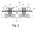
- Fig. 2 illustrates a cross-sectional view of an embodiment of print heads bonded with a substrate carrier.
- Figs. 3A-E illustrate cross-sectional representations of process steps showing bonding of an exemplary substrate and substrate carrier in accordance with one embodiment.
- Figs. 4A-H illustrate cross-sectional representations of process steps for forming portions of a fluid ejection device in accordance with one embodiment.
- Fig. 5A illustrates a process for forming electronic devices according to one embodiment.
- Fig. 5B illustrates a process for forming micro-electromechanical devices according to one embodiment.
- Fig. 5C illustrates a process for forming fluid ejection devices according to one embodiment.
- Fig. 6 illustrates a cross-sectional view of one embodiment of a MEMS device.
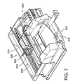
- Fig. 7 illustrates a perspective view of an embodiment of a printer.
- An electronic device 100 includes a substrate 105 and several other substrates 110 and 115 that are bonded to it.
- a layer of inorganic material 120 is formed on the surface of substrate 105 and then the combination of substrate 105 and inorganic material are subject to plasma treatment, as are substrates 110 and 115. After plasma treatment, substrates 110 and 115 are bonded to the inorganic layer 120, thereby forming a covalent bond between substrate 110 with inorganic material 120, and substrate 105, as well between each of substrate 115 with inorganic material 120, and substrate 105.
- a protective material 130 may be formed on one or more of the surface of substrates 110 and 115 that are bonded to substrate 105.
- inorganic material 120 allows for the formation of such bonds, regardless of the material that is used for substrate 105. It should be noted that inorganic material need not be applied to the entirety of the surface of substrate 105. Inorganic material 120 may be formed in any geometric pattern, for example along a perimeter of substrate 105, so that sufficient bond strength is provided while areas to on which devices may be formed are free of inorganic material 120.
- Contacts 125 are formed or otherwise provided in inorganic material 120 in order to provide conductive paths between contacts, not shown, of substrate 105 and substrates 110 and 115. Contacts 125 are generally formed prior to plasma treatment of substrate 105 and inorganic material 120. Alternatively, areas of the substrate 105 that are to be electrically coupled to areas of substrates 110 and 115 may be free of the electronic material.
- Inorganic material 120 may be any inorganic material that after being plasma treated provides an increase in the density of chemical interface species to facilitate bonding between substrate 105 and substrates 110 and 115.
- inorganic material 120 may be Tetraethyl Orthosilicate (TEOS), aluminum oxide, amorphous silicon, silicon nitride, silicon carbide, oxynitride, sapphire, indium phosphide, or a glass frit material.
- TEOS Tetraethyl Orthosilicate
- substrate 105 may be dependent on various factors including, for example, the type of electronic device being fabricated and the environment in which the electronic device is to be operated.
- Substrate 105 may be a ceramic, a glass, a semiconductor, a metal, a metal-coated structure, a polymer, combinations thereof, and others.
- Metals and metal coatings may include, for example, aluminum, chromium, copper, gold, lead, nickel, platinum, solder, stainless steel, tin, titanium, alloys thereof, combinations thereof, and others.
- Ceramics may include, for example, aluminum nitride, aluminum oxide, silicon carbide, silicon oxide, silicon oxynitride, combinations thereof, and others; alternatively aluminum nitride, aluminum oxide, silicon carbide, silicon oxynitride, and combinations thereof.
- Electronic device 100 may be any electronic device package in which a semiconductor device or similar device such as an integrated circuit is attached to a substrate, such as a chip carrier. Electronic device 100 may be part of a single chip module, a multichip module, a stacked chip module, or another device. The electronic device may be used in optoelectronic, photonic, fluid ejection, microelectromechanical, or standard integrated circuit applications.
- Fluid ejection device 200 includes a substrate carrier 205 and print heads 220.
- Substrate carrier 205 includes a first surface 210 and a second surface 215.
- a plurality of ink feed paths 245, formed in substrate carrier 205, are fluidically coupled to ink feed slots 240 formed within and/or on print heads 220.
- a second surface 215 of substrate carrier 205 includes an inorganic material 250 disposed thereon.
- Inorganic material 250 after plasma treatment, is mated to a second surface 225 of print heads 220 which opposes first surface 230.
- thin film layers (or active layers, a thin film stack, electrically conductive layers, or layers with micro-electronics) 235 are formed, e.g. deposited or grown, on a front or first side (or surface) 230 of the print heads 220.
- the first side 230 of the print heads 220 is opposite a second side (or surface) 225 of the print heads 220.
- the thin film layers 235 includes at least one layer formed on the print heads 220, and, in a particular embodiment, masks at least a portion of the first side 230 of the print heads 220.
- the one or more of the thin film layers 235 electrically insulate at least a portion of the first surface 230 of the print heads 220.
- Substrate carrier 205 may be a ceramic, a metal, a metal-coated structure, a polymer, combinations thereof, or others.
- Metals and metal coatings may include, for example, aluminum, chromium, copper, gold, lead, nickel, platinum, solder, stainless steel, tin, titanium, alloys thereof, combinations thereof, and others.
- Ceramics may include, for example, aluminum nitride, aluminum oxide, silicon carbide, silicon oxide, silicon oxynitride, combinations thereof, and others; alternatively aluminum nitride, aluminum oxide, silicon carbide, silicon oxynitride, and combinations thereof.
- the print heads 220 are silicon.
- the print heads may be one of the following: single crystalline silicon, polycrystalline silicon, gallium arsenide, glass, silica, ceramics, or a semiconductor material.
- the various materials listed as possible substrate materials are not necessarily interchangeable and are selected depending upon the application for which they are to be used.
- inorganic material 250 need not be present and second surface 215 of substrate carrier 205 may be directly mated with second surface 225 of print heads 220.
- both substrate carrier 205 and print heads 220 may comprise a semiconductor material.
- a substrate carrier or other substrate structure 300 includes a first surface 305 and a second surface 310 substantially opposing first surface 305 ( Fig. 3A ).
- An inorganic material 315 is applied to second surface 310 ( Fig. 3B ).
- the inorganic material 315 may be applied, in certain embodiments, by physical vapor deposition (PVD), chemical vapor deposition (CVD), e.g. plasma-enhanced CVD, low temperature CVD, low-pressure CVD, or electron beam deposition.
- PVD physical vapor deposition
- CVD chemical vapor deposition
- plasma-enhanced CVD e.g. plasma-enhanced CVD, low temperature CVD, low-pressure CVD, or electron beam deposition.
- the inorganic material 315 is planarized and one or more contacts 320 and 325 are formed therein to allow contact with electrical contacts formed on or in first surface 305 of substrate structure 300 ( Fig. 3C ).
- Planarization can be performed by, for example, chemical mechanical polishing, as is known.
- chemical mechanical polishing may result in a surface 330 of inorganic material 315 that has a roughness of no greater than a two-nanometer variation root mean squared over a four micron square area of surface 330.
- inorganic material 315 on substrate 300 is treated by utilizing a plasma treatment process.
- the plasma treatment process comprises utilizing an inductively plasma chamber where the substrate structure is biased at approximately 120 watts, while high density plasma is generated by an inductive coil upstream with approximately 500 watts power.
- various types of plasma treatment processes may be used, including, but not limited to, corona discharge treatment, dielectric barrier discharge treatment, and glow discharge treatment. Glow discharge treatment can be carried out using plasma selected from low pressure glow discharge or atmospheric pressure glow discharge.
- plasma treatment may be performed at atmospheric pressure in a continuous process using appropriate atmospheric plasma apparatuses. Other plasma treatment processes may also be used.
- plasma treatment may be carried out at a pressure of up to about atmospheric pressure.
- plasma treatment lasts about one hundred seconds. In other embodiments, the length of plasma treatment depends on various factors including the material to be treated, the contact conditions selected, the mode of plasma treatment (e.g., batch vs. continuous), and the design of the plasma apparatus. Plasma treatment is carried out for a time sufficient to render the surface of the material to be treated sufficiently reactive to form a high density covalent bond.
- the gas utilized during plasma treatment may be nitrogen, oxygen, argon, or combinations thereof:
- the gas used in plasma treatment may be air, ammonia, carbon dioxide, carbon monoxide, helium, hydrogen, nitrous oxide, ozone, water vapor, combinations thereof, and others.
- the gas utilized may be selected from air, carbon dioxide, carbon monoxide, helium, nitrogen, nitrous oxide, ozone, water vapor, and combinations thereof.
- the gas may be selected from air, argon, carbon dioxide, helium, nitrogen, ozone, and combinations thereof.
- a wet treatment is applied to the surface or surfaces which have been subject to plasma treatment for substrate cleaning and hydrophilization treatment for bonding.
- the wet treatment may utilize a liquid that comprises deionized water.
- the liquid utilized may comprise SC1, which may have a structure (25 H 2 O: 2 H 2 O 2 : 1 NH 4 OH).
- SC1 may have a structure (25 H 2 O: 2 H 2 O 2 : 1 NH 4 OH).
- SC1 When SC1 is utilized, the SC1 renders the surface hydrophilic and creates a terminated -OH group.
- the utilization of a wet treatment may provide benefits such that when two hydrophilic surfaces are brought into contact at room temperature, substrates form a hydrogen bond spontaneously.
- the substrates 335 and 340 may include one or more structures 355 and 370 formed on respective first surfaces 350 and 365. These structures 355 and 370 may comprise sensors, optical, electrical, or electromechanical structures or circuits that perform different functions as desired.
- the second surfaces 345 and 360, respectively, of substrates 335 and 340 are then subject to a plasma treatment process, similar to those that is utilized for inorganic material 315 and substrate structure 300.
- Substrates 335 and 340 are then mated with inorganic material 315 on substrate 300. Mating may utilize a pick and place tool, as is known, to position substrates 335 and 340 and substrate structure 300 so that proper alignment is achieved. For instance, the contacts or fluid paths in substrates 335 and 340 are properly aligned with corresponding structures in inorganic material 315 and substrate structure 300.
- mating of substrates 335 and 340 and inorganic material 315 and substrate structure 300 may occur immediately after wet treatment on inorganic material 315 and substrate structure 300. In other embodiments, mating may occur within approximately twenty-four hours of the application of fluid.
- the mated structure is annealed.
- annealing temperatures below approximately four hundred degrees Celsius to prevent the development of a built-in stress in the package or so that the degradation of CMOS devices can be avoided.
- Figs. 3A-3E discusses wet-treatment after plasma treatments, such actions need not be utilized. In other embodiments, it is also possible to plasma treat and bond substrates 335 and 340 and substrate structure 300 without wet-treatment, and mating them immediately. In an alternative embodiment, the surface may also be hydrated by exposing the surface to a moisture source during or after plasma treatment. This approach may be beneficial for certain types of MEMS packaging since it does not introduce any moisture to the package.
- a substrate 400 includes thin film layers 415 formed on a first surface 410.
- a number of chambers 430 are formed in thin film layers 415.
- the chambers 430 include a volume of fluid that is to be ejected based upon signals provided to the thin film layers 415.
- a protective layer 420 is formed over thin film layers 415 in order to protect thin film layers 415 during processing of substrate 400.
- a protective layer 435 is also provided on the second surface 425 of substrate 400 in order to protect portions of the backside surface 425 that are not subject to processing.
- second surface 425 is planarized, e.g. by a chemical mechanical polishing process, prior to application of protective layer 435.
- substrate 400 comprises a double-sided polished wafer prior to processing.
- protective layer 435 may comprise a nitride, carbide, or oxide layer as is known.
- fluid channels 440 and 445 are formed via a process method formed through second surface 425.
- processes such as laser ablation, wet etching, dry etching, and mechanically removing such as abrasive jet machining and sawing, or combinations thereof.
- fluid channels 440 and 445 are further formed to have a desired shape that is consistent with the desired fluid flow.
- the shaping of fluid channels 440 and 445 may be performed by, for example, a wet etch process. Further, fluid channels 440 and 445 may shaped after fluid channels 440 and 445 form through channels between first surface 410 and second surface 425. In addition, it is possible that a trench is formed in portions of first surface 410 through which fluid channels 440 and 445 are to be formed prior to formation of the fluid channels 440 and 445 through second surface 425. Further, the shape and geometry of fluid channels may be different than that which is depicted in Figs. 4A-4H .
- a substrate carrier 450 includes fluid paths 470 and 475 therein that are to provide fluid to fluid channels 440 and 445 of substrate 400.
- Fluid paths 470 and 475 provide fluid flow paths between a first surface 455 and a second surface 465 of substrate carrier 450.
- fluid paths 470 and 475 are fluidically coupled to a fluid supply that is to supply fluid for ejection from the chambers 430 formed on substrate 400.
- Substrate carrier 450 may comprise, for example, ceramic, metal or other material.
- An inorganic material 460 is applied to a first surface 455 in order to facilitate bonding of the wafer 400 and the substrate carrier 450.
- inorganic material 460 may comprise TEOS, aluminum oxide, amorphous silicon, silicon nitride, silicon carbide, oxynitride, indium phosphide, sapphire, and a glass frit material, amongst others.
- Inorganic material 460 is then planarized, Fig. 4E , and any material that may have been provided such that it blocks fluid paths 470 and 475 is removed.
- planarization is performed in order to strengthen the bond between substrate 400 and substrate carrier 450.
- a roughness of inorganic material 460, after planarization is no greater than a two-nanometer root mean squared variation over a four micron square area.
- inorganic material 460 on first surface 455 of substrate carrier 450 and second surface 435 of substrate 400 are subject to a plasma treatment process.
- the plasma treatment processes may be similar to those described and discussed with respect to Figs. 3A-3E . Further, plasma treatment of inorganic material 460 on first surface 455 of substrate carrier 450 and second surface 425 of substrate 400 may occur at the same or different times.
- protective material 435 is removed prior to plasma treatment of second surface 425.
- wet treatment is done to the inorganic material 460 for cleaning and hydrophilization treatment for bonding.
- the wet treatment may utilize a liquid that may comprise deionized water.
- the liquid may comprise SC1, which may have a structure (25 H 2 O: 2 H 2 O 2 : 1 NH 4 OH).
- the second surface 425 is mated to the inorganic material 460 on first surface 455, Fig. 4H .
- Mating may be performed by, for example, a pick and place tool.
- the mated structure is then annealed. Annealing may take place at temperatures greater than approximately one hundred ten degrees Celsius. In other embodiments, the annealing temperature may be approximately two hundred degrees Celsius.
- FIG. 5A a process for forming electronic devices according to one embodiment is illustrated.
- An inorganic material is applied to a surface, to which a substrate is to be bonded, of a substrate carrier or fixture, block 500.
- the inorganic material is then planarized, block 505.
- planarization is performed so that the inorganic material has a height variation of no greater than a two-nanometers root-mean-squared over a four micron square area. In other embodiments, other height variations, using the same or different measures, may be utilized.
- the planarized inorganic material is subject to plasma treatment, block 510.
- the substrates, or substrates, that are to be bonded to the substrate carrier or fixture, are also plasma treated, block 515.
- the plasma treatment of both the substrate and substrate carrier may use the same or different processes and may occur at the same or different times.
- wet treatment is applied to the inorganic material for substrate cleaning and hydrophilization treatment, block 520. Such wet treatment may also be applied to the substrate, in certain embodiments.
- the substrate carrier surface with the inorganic material thereon and the substrate are mated together, after plasma treatment, block 525.
- the mated substrate carrier and substrate are then annealed in order to promote covalent bonding between the inorganic material and the substrate, block 530.
- a MEMS device is fabricated, block 550.
- MEMS device may be fabricated utilizing any know process or any combination of known processes.
- An inorganic material is then applied to one or more surfaces of the MEMS device that are to be bonded to a carrier or support structure, block 555.
- the same or different inorganic material is also applied to a surface or surfaces of a structure that is to be bonded with the MEMS device, block 560.
- Planarization, blocks 565 and 575 respectively, may be performed so that the inorganic material has a height variation of approximately no greater than a two-nanometers root-mean-squared over a four micron square area is provided.
- an atomic layer or other deposition may be utilized that provides the desired height variations over small areas, e.g. four micron areas, of the structures that facilitate bonding of the MEMS device and carrier or support structure.
- the inorganic material of the MEMS device having the desired height variation, is subject to plasma treatment, block 585.
- the inorganic material of the carrier or support structure, having the desired height variation over small areas, is also plasma treated, block 580.
- the plasma treatment of both the support structure and MEMS device may use the same or different processes and may occur at the same or different times.
- a wet treatment is applied to the plasma treated inorganic material, block 585. Such wet treatment may also be applied to the substrate, in certain embodiments.
- the MEMS device with the inorganic material thereon and the support structure are mated together, block 590.
- the mated structure is then annealed in order to promote covalent bonding, block 595.
- a fluid ejection device such as a print head, includes a number of fluid ejection elements formed on a surface of a substrate.
- the surface of the substrate opposing the surface on which the fluid ejection elements are formed is plasma treated, block 600.
- a substrate carrier that is to provide fluid paths to the fluid ejection elements and electrical connection to a control device is plasma treated, block 605.
- the treatment may be of a surface that is to be bonded to the surface of the substrate.
- an inorganic material need not be applied to either the surfaces of the substrate or substrate carrier that are to be bonded together.
- the substrate carrier and substrate may comprise a semiconductor material such as silicon.
- the surface of the substrate that has been plasma treated is then subject to a wet treatment, block 610. Also, the surface of the substrate carrier that has been plasma treated is subject to a wet treatment, block 615. The timing of the wet treatment may be simultaneous or occur at different times.
- the wet treated surface of the substrate and the wet treated surface of the substrate carrier are mated together, block 620. The mated structure is then annealed, block 625.
- one or both of the surface of the substrate and surface of the substrate carrier that are to be subject to plasma treatment may be planarized prior to plasma treatment.
- micro-electromechanical device 600 may be an optoelectrical device.
- micro-electromechanical device 700 may be pressure sensor, photonic, fluid ejection, or other micro-electromechanical that comprises multiple substrates bonded to each other or a substrate bonded to a carrier structure.
- an optical device 705 is formed on a substrate 710 that includes electrical components for receiving signals from or transmitting signals to electrical components, as well as other processing functions.
- a membrane of optical energy transmissive inorganic material 715 may surround optical device 705 for protection of optical device 705.
- a transmissive material 725, with an inorganic material 720 formed thereon is bonded to inorganic material 715.
- transmissive material 725 may be provided to attenuate optical energy and/or to protect optical device 705 from the external environment.
- transmissive material 725 may be glass or a mixture of glass and one or more other materials.
- An anti-reflective coating 730 may be applied to a surface or surfaces of transmissive material 725 that interact with an external environment.
- Micro-electromechanical device 700 may be utilized as an optical switch, as a mirror element for a light projector, or other optical device.
- micro-electromechanical device 700 may comprise a photonic, a device including mechanically deformable elements, signal transmission elements or combinations therefore.
- the printing device comprises a printer 800.
- the printer shown here is embodied in the form of an inkjet printer.
- the printer 800 can be capable of printing in black-and-white and/or in color.
- the term "printing device" refers to any type of printing device and/or image forming device that employs slotted substrate(s) to achieve at least a portion of its functionality. Examples of such printing devices can include, but are not limited to, printers, facsimile machines, and photocopiers.
- the slotted substrates comprise a portion of a print head which is incorporated into a print cartridge, an example of which is described below.
- FIG. 7 illustrates a printer with a print cartridge according to one embodiment.
- printer 800 can incorporate one or more print cartridges 810, which is a type of fluid ejection device.
- Printer 800 can also include a tray 805 for holding print media.
- print media such as paper
- the sheet then brought around in a U direction and travels in an opposite direction toward output tray 815.
- Other paper paths such as a straight paper path, can also be used.
- the sheet is stopped in a print zone 820, and a scanning carriage 825, supporting one or more print cartridges 810, is then scanned across the sheet for printing a swath of ink thereon.
- the sheet is then incrementally shifted using, for example, a stepper motor and feed rollers to a next position within the print zone 820.
- Carriage 825 again scans across the sheet for printing a next swath of ink. The process repeats until the entire sheet has been printed, at which point it is ejected into output tray 815.
- the print cartridges 810 can be removeably mounted or permanently mounted to the scanning carriage 825.
- the print cartridges 810 can have self-contained ink reservoirs (for example, the reservoir can be located within print head assembly body, e.g. the embodiment of fluid ejection device 5 in FIG. 1 .)
- the self-contained ink reservoirs can be refilled with ink for reusing the print cartridges 810.
- each print cartridge 810 can be fluidly coupled, via a flexible conduit 830, to one of a plurality of fixed or removable ink supplies 835 acting as the ink supply.
- the ink supplies 835 can be one or more ink containers separate or separable from print head assemblies.
- the substrate may comprise a print head. In embodiments of the invention defined in claim 4, the substrate may be configured to eject ink from the ink ejection elements.
- the first substrate may comprise silicon and the second substrate may comprise a ceramic.
- the electronic elements may comprise fluid ejection elements.
- Embodiments of the invention defined in claim 5 may further comprise a third substrate comprising a first surface and a second surface, wherein the means for covalently bonding comprises means for covalently bonding a first portion of the second surface of the second substrate to the second surface of the first substrate and a second portion of the second surface of the substrate to the second surface of the third substrate.
- the first substrate comprises silicon and the second substrate carrier comprises a ceramic.
- the second surface of the substrate carrier may comprise a variation of height of no more than approximately two nanometers root-mean-squared over any four micron squared area of the second surface.
- Embodiments of the invention defined in claim 8 may comprise another substrate comprising a first surface and a second surface, wherein first portion of the second surface of the substrate carrier bonds to the second surface of the first substrate and a second portion of the second surface of the substrate carrier to the second surface of the substrate carrier bonds to the second surface of the another substrate.
Landscapes
- Engineering & Computer Science (AREA)
- Manufacturing & Machinery (AREA)
- Microelectronics & Electronic Packaging (AREA)
- Physics & Mathematics (AREA)
- Optics & Photonics (AREA)
- Micromachines (AREA)
- Particle Formation And Scattering Control In Inkjet Printers (AREA)
Abstract
Description
- The market for electronic devices continually demands higher performance at lower costs. In order to meet these requirements the components which comprise various electronic devices need to be made more efficiently and to closer tolerances.
- In certain electronic devices a silicon substrate is bonded or otherwise coupled to another substrate or substrate carrier to form a completed device. In such instances, the electronic device is often exposed to harsh conditions and corrosive materials. In known devices, a substrate is bonded to a substrate carrier by using an organic, often a polymeric based, adhesive or adherent. However, over time, due to environmental conditions such as the presence of solvents, to which the adhesive is exposed, the bond may be partially damaged or completely broken. In turn, this may result in the exposure of sensitive electronic components to the environment. These components would then be damaged and the device potentially rendered non-functional.
- One application where a substrate is bonded to a carrier is a fluid ejection device, such as ink jet print head. In these devices a substrate containing multiple fluid ejection elements is often bonded to a substrate carrier.
-
Fig. 1 illustrates a cross-sectional view of one embodiment of an electronic device. -
Fig. 2 illustrates a cross-sectional view of an embodiment of print heads bonded with a substrate carrier. -
Figs. 3A-E illustrate cross-sectional representations of process steps showing bonding of an exemplary substrate and substrate carrier in accordance with one embodiment. -
Figs. 4A-H illustrate cross-sectional representations of process steps for forming portions of a fluid ejection device in accordance with one embodiment. -
Fig. 5A illustrates a process for forming electronic devices according to one embodiment. -
Fig. 5B illustrates a process for forming micro-electromechanical devices according to one embodiment. -
Fig. 5C illustrates a process for forming fluid ejection devices according to one embodiment. -
Fig. 6 illustrates a cross-sectional view of one embodiment of a MEMS device. -
Fig. 7 illustrates a perspective view of an embodiment of a printer. - Examples of particular feature size, shape, and arrangement are depicted herein. However, any type of feature size and geometry may be fabricated using the inventive methods and apparatuses described herein.
- Referring to
Fig. 1 , a cross-sectional view of one embodiment of an electronic device is illustrated. Anelectronic device 100 includes asubstrate 105 and severalother substrates inorganic material 120 is formed on the surface ofsubstrate 105 and then the combination ofsubstrate 105 and inorganic material are subject to plasma treatment, as aresubstrates substrates inorganic layer 120, thereby forming a covalent bond betweensubstrate 110 withinorganic material 120, andsubstrate 105, as well between each ofsubstrate 115 withinorganic material 120, andsubstrate 105. - In one embodiment, a
protective material 130 may be formed on one or more of the surface ofsubstrates substrate 105. - In certain embodiments, by utilizing plasma-enhanced bonding the substrates are joined directly at the atomic-level with robust covalent siloxane bonds. In such embodiments, the utilization of
inorganic material 120 allows for the formation of such bonds, regardless of the material that is used forsubstrate 105. It should be noted that inorganic material need not be applied to the entirety of the surface ofsubstrate 105.Inorganic material 120 may be formed in any geometric pattern, for example along a perimeter ofsubstrate 105, so that sufficient bond strength is provided while areas to on which devices may be formed are free ofinorganic material 120. -
Contacts 125 are formed or otherwise provided ininorganic material 120 in order to provide conductive paths between contacts, not shown, ofsubstrate 105 andsubstrates Contacts 125 are generally formed prior to plasma treatment ofsubstrate 105 andinorganic material 120. Alternatively, areas of thesubstrate 105 that are to be electrically coupled to areas ofsubstrates -
Inorganic material 120 may be any inorganic material that after being plasma treated provides an increase in the density of chemical interface species to facilitate bonding betweensubstrate 105 andsubstrates inorganic material 120 may be Tetraethyl Orthosilicate (TEOS), aluminum oxide, amorphous silicon, silicon nitride, silicon carbide, oxynitride, sapphire, indium phosphide, or a glass frit material. - The material(s) for forming
substrate 105 may be dependent on various factors including, for example, the type of electronic device being fabricated and the environment in which the electronic device is to be operated.Substrate 105 may be a ceramic, a glass, a semiconductor, a metal, a metal-coated structure, a polymer, combinations thereof, and others. Metals and metal coatings may include, for example, aluminum, chromium, copper, gold, lead, nickel, platinum, solder, stainless steel, tin, titanium, alloys thereof, combinations thereof, and others. Ceramics may include, for example, aluminum nitride, aluminum oxide, silicon carbide, silicon oxide, silicon oxynitride, combinations thereof, and others; alternatively aluminum nitride, aluminum oxide, silicon carbide, silicon oxynitride, and combinations thereof. -
Electronic device 100 may be any electronic device package in which a semiconductor device or similar device such as an integrated circuit is attached to a substrate, such as a chip carrier.Electronic device 100 may be part of a single chip module, a multichip module, a stacked chip module, or another device. The electronic device may be used in optoelectronic, photonic, fluid ejection, microelectromechanical, or standard integrated circuit applications. - Referring to
Fig. 2 , a cross-sectional view of an embodiment of print heads bonded with a substrate carrier is illustrated.Fluid ejection device 200 includes asubstrate carrier 205 andprint heads 220.Substrate carrier 205 includes afirst surface 210 and asecond surface 215. A plurality ofink feed paths 245, formed insubstrate carrier 205, are fluidically coupled toink feed slots 240 formed within and/or onprint heads 220. - A
second surface 215 ofsubstrate carrier 205 includes aninorganic material 250 disposed thereon.Inorganic material 250, after plasma treatment, is mated to asecond surface 225 ofprint heads 220 which opposesfirst surface 230. - In
Fig. 2 , thin film layers (or active layers, a thin film stack, electrically conductive layers, or layers with micro-electronics) 235 are formed, e.g. deposited or grown, on a front or first side (or surface) 230 of theprint heads 220. Thefirst side 230 of theprint heads 220 is opposite a second side (or surface) 225 of theprint heads 220. Thethin film layers 235 includes at least one layer formed on theprint heads 220, and, in a particular embodiment, masks at least a portion of thefirst side 230 of theprint heads 220. Alternatively or additionally, the one or more of thethin film layers 235 electrically insulate at least a portion of thefirst surface 230 of theprint heads 220. -
Substrate carrier 205 may be a ceramic, a metal, a metal-coated structure, a polymer, combinations thereof, or others. Metals and metal coatings may include, for example, aluminum, chromium, copper, gold, lead, nickel, platinum, solder, stainless steel, tin, titanium, alloys thereof, combinations thereof, and others. Ceramics may include, for example, aluminum nitride, aluminum oxide, silicon carbide, silicon oxide, silicon oxynitride, combinations thereof, and others; alternatively aluminum nitride, aluminum oxide, silicon carbide, silicon oxynitride, and combinations thereof. - In one embodiment, the
print heads 220 are silicon. In various embodiments, the print heads may be one of the following: single crystalline silicon, polycrystalline silicon, gallium arsenide, glass, silica, ceramics, or a semiconductor material. The various materials listed as possible substrate materials are not necessarily interchangeable and are selected depending upon the application for which they are to be used. - In certain embodiments,
inorganic material 250 need not be present andsecond surface 215 ofsubstrate carrier 205 may be directly mated withsecond surface 225 of print heads 220. In such embodiments, bothsubstrate carrier 205 andprint heads 220 may comprise a semiconductor material. - Referring to
Figs. 3A-3E , cross-sectional representations of process steps for forming a fluid ejection device in accordance with one embodiment are illustrated. A substrate carrier orother substrate structure 300 includes afirst surface 305 and asecond surface 310 substantially opposing first surface 305 (Fig. 3A ). - An
inorganic material 315 is applied to second surface 310 (Fig. 3B ). Theinorganic material 315 may be applied, in certain embodiments, by physical vapor deposition (PVD), chemical vapor deposition (CVD), e.g. plasma-enhanced CVD, low temperature CVD, low-pressure CVD, or electron beam deposition. - After deposition, the
inorganic material 315 is planarized and one ormore contacts first surface 305 of substrate structure 300 (Fig. 3C ). Planarization can be performed by, for example, chemical mechanical polishing, as is known. In certain embodiments, chemical mechanical polishing may result in asurface 330 ofinorganic material 315 that has a roughness of no greater than a two-nanometer variation root mean squared over a four micron square area ofsurface 330. - After planarization,
inorganic material 315 onsubstrate 300 is treated by utilizing a plasma treatment process. In one embodiment the plasma treatment process comprises utilizing an inductively plasma chamber where the substrate structure is biased at approximately 120 watts, while high density plasma is generated by an inductive coil upstream with approximately 500 watts power. In other embodiments, various types of plasma treatment processes may be used, including, but not limited to, corona discharge treatment, dielectric barrier discharge treatment, and glow discharge treatment. Glow discharge treatment can be carried out using plasma selected from low pressure glow discharge or atmospheric pressure glow discharge. In certain embodiments, plasma treatment may be performed at atmospheric pressure in a continuous process using appropriate atmospheric plasma apparatuses. Other plasma treatment processes may also be used. - The exact conditions for plasma treatment will vary depending on various factors including the choice of material, the storage time between plasma treatment and bonding, the type and method of plasma treatment used, the design of the plasma chamber used, and others. However, in certain embodiments plasma treatment may be carried out at a pressure of up to about atmospheric pressure.
- In one embodiment plasma treatment lasts about one hundred seconds. In other embodiments, the length of plasma treatment depends on various factors including the material to be treated, the contact conditions selected, the mode of plasma treatment (e.g., batch vs. continuous), and the design of the plasma apparatus. Plasma treatment is carried out for a time sufficient to render the surface of the material to be treated sufficiently reactive to form a high density covalent bond.
- In one embodiment, the gas utilized during plasma treatment may be nitrogen, oxygen, argon, or combinations thereof: In other embodiments, the gas used in plasma treatment may be air, ammonia, carbon dioxide, carbon monoxide, helium, hydrogen, nitrous oxide, ozone, water vapor, combinations thereof, and others. Additionally, the gas utilized may be selected from air, carbon dioxide, carbon monoxide, helium, nitrogen, nitrous oxide, ozone, water vapor, and combinations thereof. Alternatively, the gas may be selected from air, argon, carbon dioxide, helium, nitrogen, ozone, and combinations thereof. Alternatively, other more reactive organic gases or vapors can be used, either in their normal state of gases at the process application pressure or vaporized with a suitable device from otherwise liquid states, such as hexamethyldisiloxane, cyclopolydimethylsiloxane, cyclopolyhydrogenmethylsiloxanes, cyclopolyhydrogenmethyl-co-dimethylsilo- xanes, reactive silanes, combinations thereof, and others.
- After plasma treatment, a wet treatment is applied to the surface or surfaces which have been subject to plasma treatment for substrate cleaning and hydrophilization treatment for bonding. In certain embodiments, the wet treatment may utilize a liquid that comprises deionized water. In other embodiments, the liquid utilized may comprise SC1, which may have a structure (25 H2O: 2 H2O2: 1 NH4OH). The surface will be exposed to SC1 fluid for 40 seconds, rinsed with deionized water, and then dried in air or nitrogen. When SC1 is utilized, the SC1 renders the surface hydrophilic and creates a terminated -OH group. The utilization of a wet treatment may provide benefits such that when two hydrophilic surfaces are brought into contact at room temperature, substrates form a hydrogen bond spontaneously.
- One or
more substrates Fig. 3D ). Thesubstrates more structures first surfaces structures second surfaces substrates inorganic material 315 andsubstrate structure 300. -
Substrates inorganic material 315 onsubstrate 300. Mating may utilize a pick and place tool, as is known, to positionsubstrates substrate structure 300 so that proper alignment is achieved. For instance, the contacts or fluid paths insubstrates inorganic material 315 andsubstrate structure 300. - In certain embodiments, mating of
substrates inorganic material 315 andsubstrate structure 300 may occur immediately after wet treatment oninorganic material 315 andsubstrate structure 300. In other embodiments, mating may occur within approximately twenty-four hours of the application of fluid. - After mating, the mated structure is annealed. Annealing may take place at temperatures greater than approximately one hundred ten degrees Celsius. In other embodiments, the annealing temperature may be approximately two hundred degrees Celsius. It is believed that, in certain embodiments, annealing may cause water molecules to start leaving the interface between
inorganic material 315 and thesecond surfaces substrates - In certain embodiments, e.g. in MEMS applications, it may be desirable to keep annealing temperatures below approximately four hundred degrees Celsius to prevent the development of a built-in stress in the package or so that the degradation of CMOS devices can be avoided.
- While the description with respect to
Figs. 3A-3E discusses wet-treatment after plasma treatments, such actions need not be utilized. In other embodiments, it is also possible to plasma treat andbond substrates substrate structure 300 without wet-treatment, and mating them immediately. In an alternative embodiment, the surface may also be hydrated by exposing the surface to a moisture source during or after plasma treatment. This approach may be beneficial for certain types of MEMS packaging since it does not introduce any moisture to the package. - It is believed that the approach described with respect to
Figs. 3A-E allows for a bond that joins two substrates directly at the atomic-level with a robust covalent siloxane bonds. - Referring to
Figs. 4A-4H , cross-sectional representations of process steps for forming portions of a fluid ejection device in accordance with one embodiment are illustrated. Asubstrate 400 includes thin film layers 415 formed on afirst surface 410. A number ofchambers 430 are formed in thin film layers 415. Thechambers 430 include a volume of fluid that is to be ejected based upon signals provided to the thin film layers 415. Aprotective layer 420 is formed over thin film layers 415 in order to protect thin film layers 415 during processing ofsubstrate 400. - A
protective layer 435 is also provided on thesecond surface 425 ofsubstrate 400 in order to protect portions of thebackside surface 425 that are not subject to processing. In certain embodiments,second surface 425 is planarized, e.g. by a chemical mechanical polishing process, prior to application ofprotective layer 435. In other embodiments,substrate 400 comprises a double-sided polished wafer prior to processing. In some embodiments,protective layer 435 may comprise a nitride, carbide, or oxide layer as is known. - In
Fig. 4B ,fluid channels second surface 425. In some embodiments, processes such as laser ablation, wet etching, dry etching, and mechanically removing such as abrasive jet machining and sawing, or combinations thereof. - In
Fig. 4C ,fluid channels fluid channels fluid channels fluid channels first surface 410 andsecond surface 425. In addition, it is possible that a trench is formed in portions offirst surface 410 through whichfluid channels fluid channels second surface 425. Further, the shape and geometry of fluid channels may be different than that which is depicted inFigs. 4A-4H . - In
Fig. 4D , asubstrate carrier 450 includesfluid paths fluid channels substrate 400.Fluid paths first surface 455 and asecond surface 465 ofsubstrate carrier 450. Atsecond surface 465,fluid paths chambers 430 formed onsubstrate 400. -
Substrate carrier 450 may comprise, for example, ceramic, metal or other material. Aninorganic material 460 is applied to afirst surface 455 in order to facilitate bonding of thewafer 400 and thesubstrate carrier 450. In certain embodiments,inorganic material 460 may comprise TEOS, aluminum oxide, amorphous silicon, silicon nitride, silicon carbide, oxynitride, indium phosphide, sapphire, and a glass frit material, amongst others. -
Inorganic material 460 is then planarized,Fig. 4E , and any material that may have been provided such that it blocksfluid paths substrate 400 andsubstrate carrier 450. In some embodiments, a roughness ofinorganic material 460, after planarization, is no greater than a two-nanometer root mean squared variation over a four micron square area. - In
Figs. 4F and 4G ,inorganic material 460 onfirst surface 455 ofsubstrate carrier 450 andsecond surface 435 ofsubstrate 400 are subject to a plasma treatment process. The plasma treatment processes may be similar to those described and discussed with respect toFigs. 3A-3E . Further, plasma treatment ofinorganic material 460 onfirst surface 455 ofsubstrate carrier 450 andsecond surface 425 ofsubstrate 400 may occur at the same or different times. - It should be noted that
protective material 435 is removed prior to plasma treatment ofsecond surface 425. - After, plasma treatment, wet treatment is done to the
inorganic material 460 for cleaning and hydrophilization treatment for bonding. In certain embodiments, the wet treatment may utilize a liquid that may comprise deionized water. In other embodiments, the liquid may comprise SC1, which may have a structure (25 H2O: 2 H2O2: 1 NH4OH). - After the wet treatment is done to inorganic material, the
second surface 425 is mated to theinorganic material 460 onfirst surface 455,Fig. 4H . Mating may be performed by, for example, a pick and place tool. The mated structure is then annealed. Annealing may take place at temperatures greater than approximately one hundred ten degrees Celsius. In other embodiments, the annealing temperature may be approximately two hundred degrees Celsius. - Referring to
Fig. 5A , a process for forming electronic devices according to one embodiment is illustrated. An inorganic material is applied to a surface, to which a substrate is to be bonded, of a substrate carrier or fixture, block 500. The inorganic material is then planarized, block 505. In one embodiment, planarization is performed so that the inorganic material has a height variation of no greater than a two-nanometers root-mean-squared over a four micron square area. In other embodiments, other height variations, using the same or different measures, may be utilized. - The planarized inorganic material is subject to plasma treatment, block 510. The substrates, or substrates, that are to be bonded to the substrate carrier or fixture, are also plasma treated, block 515. The plasma treatment of both the substrate and substrate carrier may use the same or different processes and may occur at the same or different times. After plasma treatment, wet treatment is applied to the inorganic material for substrate cleaning and hydrophilization treatment, block 520. Such wet treatment may also be applied to the substrate, in certain embodiments.
- The substrate carrier surface with the inorganic material thereon and the substrate are mated together, after plasma treatment, block 525. The mated substrate carrier and substrate are then annealed in order to promote covalent bonding between the inorganic material and the substrate, block 530.
- Referring to
Fig. 5B , a process for forming micro-electromechanical devices is illustrated. A MEMS device is fabricated, block 550. MEMS device may be fabricated utilizing any know process or any combination of known processes. An inorganic material is then applied to one or more surfaces of the MEMS device that are to be bonded to a carrier or support structure, block 555. The same or different inorganic material is also applied to a surface or surfaces of a structure that is to be bonded with the MEMS device, block 560. Planarization, blocks 565 and 575 respectively, may be performed so that the inorganic material has a height variation of approximately no greater than a two-nanometers root-mean-squared over a four micron square area is provided. In other embodiments, an atomic layer or other deposition may be utilized that provides the desired height variations over small areas, e.g. four micron areas, of the structures that facilitate bonding of the MEMS device and carrier or support structure. - The inorganic material of the MEMS device, having the desired height variation, is subject to plasma treatment, block 585. The inorganic material of the carrier or support structure, having the desired height variation over small areas, is also plasma treated, block 580. The plasma treatment of both the support structure and MEMS device may use the same or different processes and may occur at the same or different times. A wet treatment is applied to the plasma treated inorganic material, block 585. Such wet treatment may also be applied to the substrate, in certain embodiments.
- The MEMS device with the inorganic material thereon and the support structure are mated together, block 590. The mated structure is then annealed in order to promote covalent bonding, block 595.
- Referring to
Fig. 5C , a process for forming fluid ejection devices according to one embodiment is illustrated. A fluid ejection device, such as a print head, includes a number of fluid ejection elements formed on a surface of a substrate. The surface of the substrate opposing the surface on which the fluid ejection elements are formed is plasma treated, block 600. Also, a substrate carrier that is to provide fluid paths to the fluid ejection elements and electrical connection to a control device is plasma treated, block 605. The treatment may be of a surface that is to be bonded to the surface of the substrate. - In certain embodiments, an inorganic material need not be applied to either the surfaces of the substrate or substrate carrier that are to be bonded together. In such embodiments, the substrate carrier and substrate may comprise a semiconductor material such as silicon.
- The surface of the substrate that has been plasma treated is then subject to a wet treatment, block 610. Also, the surface of the substrate carrier that has been plasma treated is subject to a wet treatment, block 615. The timing of the wet treatment may be simultaneous or occur at different times. The wet treated surface of the substrate and the wet treated surface of the substrate carrier are mated together, block 620. The mated structure is then annealed, block 625.
- It should be noted, that in certain embodiments that one or both of the surface of the substrate and surface of the substrate carrier that are to be subject to plasma treatment may be planarized prior to plasma treatment.
- Referring to
Fig. 6 , a cross-sectional view of one embodiment of a MEMS device is illustrated. In the embodiment ofFig. 6 ,micro-electromechanical device 600 may be an optoelectrical device. In other embodiments,micro-electromechanical device 700 may be pressure sensor, photonic, fluid ejection, or other micro-electromechanical that comprises multiple substrates bonded to each other or a substrate bonded to a carrier structure. - In
Fig. 6 , anoptical device 705 is formed on asubstrate 710 that includes electrical components for receiving signals from or transmitting signals to electrical components, as well as other processing functions. A membrane of optical energy transmissiveinorganic material 715 may surroundoptical device 705 for protection ofoptical device 705. Atransmissive material 725, with aninorganic material 720 formed thereon is bonded toinorganic material 715. - In one embodiment,
transmissive material 725 may be provided to attenuate optical energy and/or to protectoptical device 705 from the external environment. In certain embodiments,transmissive material 725 may be glass or a mixture of glass and one or more other materials. Ananti-reflective coating 730 may be applied to a surface or surfaces oftransmissive material 725 that interact with an external environment. -
Micro-electromechanical device 700 may be utilized as an optical switch, as a mirror element for a light projector, or other optical device. In addition,micro-electromechanical device 700 may comprise a photonic, a device including mechanically deformable elements, signal transmission elements or combinations therefore. - Referring to
Fig. 7 , a perspective view of an embodiment of a printer is illustrated. In this embodiment the printing device comprises aprinter 800. The printer shown here is embodied in the form of an inkjet printer. Theprinter 800 can be capable of printing in black-and-white and/or in color. The term "printing device" refers to any type of printing device and/or image forming device that employs slotted substrate(s) to achieve at least a portion of its functionality. Examples of such printing devices can include, but are not limited to, printers, facsimile machines, and photocopiers. In this exemplary printing device the slotted substrates comprise a portion of a print head which is incorporated into a print cartridge, an example of which is described below. -
Figure 7 illustrates a printer with a print cartridge according to one embodiment. Generally,printer 800 can incorporate one ormore print cartridges 810, which is a type of fluid ejection device.Printer 800 can also include atray 805 for holding print media. When a printing operation is initiated, print media, such as paper, is fed intoprinter 800 fromtray 805 preferably using a sheet feeder (not shown). The sheet then brought around in a U direction and travels in an opposite direction towardoutput tray 815. Other paper paths, such as a straight paper path, can also be used. The sheet is stopped in aprint zone 820, and ascanning carriage 825, supporting one ormore print cartridges 810, is then scanned across the sheet for printing a swath of ink thereon. After a single scan or multiple scans, the sheet is then incrementally shifted using, for example, a stepper motor and feed rollers to a next position within theprint zone 820.Carriage 825 again scans across the sheet for printing a next swath of ink. The process repeats until the entire sheet has been printed, at which point it is ejected intooutput tray 815. - The
print cartridges 810 can be removeably mounted or permanently mounted to thescanning carriage 825. Also, theprint cartridges 810 can have self-contained ink reservoirs (for example, the reservoir can be located within print head assembly body, e.g. the embodiment of fluid ejection device 5 inFIG. 1 .) The self-contained ink reservoirs can be refilled with ink for reusing theprint cartridges 810. Alternatively, eachprint cartridge 810 can be fluidly coupled, via aflexible conduit 830, to one of a plurality of fixed or removable ink supplies 835 acting as the ink supply. As a further alternative, the ink supplies 835 can be one or more ink containers separate or separable from print head assemblies. - In embodiments of the invention defined in claim 4, the substrate may comprise a print head. In embodiments of the invention defined in claim 4, the substrate may be configured to eject ink from the ink ejection elements.
- In embodiments of the invention defined in claim 5, the first substrate may comprise silicon and the second substrate may comprise a ceramic. In embodiments of the invention defined in claim 5, the electronic elements may comprise fluid ejection elements. Embodiments of the invention defined in claim 5 may further comprise a third substrate comprising a first surface and a second surface, wherein the means for covalently bonding comprises means for covalently bonding a first portion of the second surface of the second substrate to the second surface of the first substrate and a second portion of the second surface of the substrate to the second surface of the third substrate.
- In embodiments of the invention defined in claim 7, the first substrate comprises silicon and the second substrate carrier comprises a ceramic.
- In embodiments of the invention defined in claim 8, the second surface of the substrate carrier may comprise a variation of height of no more than approximately two nanometers root-mean-squared over any four micron squared area of the second surface. Embodiments of the invention defined in claim 8 may comprise another substrate comprising a first surface and a second surface, wherein first portion of the second surface of the substrate carrier bonds to the second surface of the first substrate and a second portion of the second surface of the substrate carrier to the second surface of the substrate carrier bonds to the second surface of the another substrate.
- Although the inventive concepts have been described in language specific to structural features and methodological steps, it is to be understood that the appended claims are not limited to the specific features or steps described. Rather, the specific features and steps are disclosed as preferred forms of implementing the inventive concepts.
Claims (15)
- An electric device (100) comprising:a substrate (110) comprising a first surface and a second surface;a substrate carrier (105) comprising a first surface and a second surface; andan inorganic material (120) bonding the second surface of the substrate and the second surface of the substrate carrier.
- The electronic device of claim 1 wherein the substrate (110, 115) comprises fluid ejection elements formed thereon.
- The electronic device of claim 1 wherein the electronic device is one an optoelectronic, photonic, fluid ejection, and microelectromechanical device.
- A fluid ejection device (200) comprising:a substrate (220) comprising a first surface including a plurality of fluid ejection elements (230) formed thereon and a second surface, and at least one fluid path (240) between the first surface and the second surface;a substrate carrier (205) comprising a first surface and a second surface, at least one fluid outlet (245) coupled with the at least one fluid path (240); andan inorganic material (250) between the second surface of the substrate (220) and the second surface of the substrate carrier (205) that bonds the second surface of the substrate (220) and the first substrate of the substrate carrier (205).
- An electronic device comprising:a first substrate (220) comprising a first surface including at least one electronic element (230) formed thereon and a second surface;a second substrate (205) comprising a first surface and a second surface; andmeans (250) for covalently bonding the second surface of the first substrate (220) and the second surface of the second substrate (205).
- The electronic device of claim 5 wherein the first substrate (220) comprises a material that changes configuration in response to an electrical current.
- A microelectromechanical device (700) comprising:a first substrate (715) comprising a first surface and a second surface;a second substrate (710) comprising a first surface and a second surface, wherein the first surface of the second substrate (710) is bonded to the second surface of the second substrate (710); anda third substrate (725) comprising a first surface and a second surface;an inorganic material (720) bonding the second surface of the third substrate (725) and the first surface of the first substrate (715)
- A fluid ejection device comprising:a substrate comprising (220) a first surface including a plurality of fluid ejection elements (230) formed thereon and a second surface that is subject to plasma treatment; anda substrate carrier (208) comprising a first surface and a second surface that is subject to plasma treatment that is bonded to the second surface of the substrate.
- The fluid ejection device of claim 8 wherein the substrate carrier comprises a semiconductor material.
- The fluid ejection device of claim 8 wherein the substrate carrier comprises at least one ink feed path (240) that is fluidically coupled at the second surface of the substrate and the second surface of the substrate carrier with at least one ink feed slot (245) formed in the substrate.
- The electronic device of claim 1 or the fluid ejection device according to claim 4 or the micromechanical device according to claim 7, wherein the inorganic material (120) is selected from a group consisting of TEOS, aluminum oxide, amorphous silicon, silicon nitride, silicon carbide, oxynitride, indium phosphide, sapphire, and a glass frit material.
- The electronic device of claim 1 or the fluid ejection device according to claim 4 or 8, wherein the substrate (110) comprises silicon and the substrate carrier (105) comprises a ceramic.
- The electronic device of claim 1 or the fluid ejection device according to claim 4 or the micromechanical device according to claim 7, wherein a surface of the inorganic material (120) being bonded to the second surface of the substrate (110, 115) comprises a variation of height of no more than approximately two nanometers root-mean-squared over any four micron squared area of the surface.
- The electronic device of claim 1 or the fluid ejection device according to claim 4 or the micromechanical device according to claim 7, further comprising another substrate (115) comprising a first surface and a second surface, wherein the inorganic material (120) bonds a first portion of the second surface of the first substrate (110) to the second surface of the substrate carrier (105) and a second portion of the second surface of the substrate carrier (105) to the second surface of the another substrate (115).
- The electronic device of claim 1 or the micromechanical device according to claim 7, wherein the substrate carrier (105) comprises a ceramic, a metal, a metal-coated structure, a polymer, and combinations thereof.
Applications Claiming Priority (3)
| Application Number | Priority Date | Filing Date | Title |
|---|---|---|---|
| US62206204P | 2004-10-26 | 2004-10-26 | |
| US10/977,141 US7563691B2 (en) | 2004-10-29 | 2004-10-29 | Method for plasma enhanced bonding and bonded structures formed by plasma enhanced bonding |
| EP05809060A EP1812238B1 (en) | 2004-10-26 | 2005-10-04 | Method for plasma enhanced bonding and bonded structures formed by plasma enhanced bonding |
Related Parent Applications (1)
| Application Number | Title | Priority Date | Filing Date |
|---|---|---|---|
| EP05809060.6 Division | 2005-10-04 |
Publications (1)
| Publication Number | Publication Date |
|---|---|
| EP2266800A1 true EP2266800A1 (en) | 2010-12-29 |
Family
ID=36262301
Family Applications (1)
| Application Number | Title | Priority Date | Filing Date |
|---|---|---|---|
| EP10185411A Withdrawn EP2266800A1 (en) | 2004-10-26 | 2005-10-04 | Method for plasma enhanced bonding and bonded structures formed by plasma enhanced bonding |
Country Status (2)
| Country | Link |
|---|---|
| US (2) | US7563691B2 (en) |
| EP (1) | EP2266800A1 (en) |
Families Citing this family (8)
| Publication number | Priority date | Publication date | Assignee | Title |
|---|---|---|---|---|
| EP1568077B1 (en) * | 2002-12-04 | 2018-07-11 | Suss MicroTec Lithography GmbH | Method for pre-treating surfaces of substrates to be bonded |
| US8217473B2 (en) * | 2005-07-29 | 2012-07-10 | Hewlett-Packard Development Company, L.P. | Micro electro-mechanical system packaging and interconnect |
| US20070023850A1 (en) * | 2005-07-30 | 2007-02-01 | Chien-Hua Chen | Bonding surfaces together via plasma treatment on both surfaces with wet treatment on only one surface |
| US8138588B2 (en) * | 2006-12-21 | 2012-03-20 | Texas Instruments Incorporated | Package stiffener and a packaged device using the same |
| WO2009088510A1 (en) * | 2008-01-09 | 2009-07-16 | Hewlett-Packard Development Company, L.P. | Fluid ejection cartridge and method |
| JP5736198B2 (en) * | 2011-03-09 | 2015-06-17 | 東芝テック株式会社 | Ink jet head and method of manufacturing ink jet head |
| JP5988612B2 (en) * | 2012-02-24 | 2016-09-07 | キヤノン株式会社 | Ink jet head and method of manufacturing ink jet head |
| US12300516B2 (en) | 2022-03-30 | 2025-05-13 | Yamaha Robotics Holdings Co., Ltd. | Wafer cleaning apparatus and bonding system |
Citations (5)
| Publication number | Priority date | Publication date | Assignee | Title |
|---|---|---|---|---|
| EP0651449A2 (en) * | 1993-11-01 | 1995-05-03 | Matsushita Electric Industrial Co., Ltd. | Electronic component and method for producing the same |
| WO2001061743A1 (en) * | 2000-02-16 | 2001-08-23 | Ziptronix, Inc. | Method for low temperature bonding and bonded structure |
| US20030081073A1 (en) * | 2001-10-31 | 2003-05-01 | Chien-Hua Chen | Fluid ejection device with a composite substrate |
| EP1329489A2 (en) * | 2002-01-18 | 2003-07-23 | Hewlett-Packard Company | Method of preparing a surface for adhesion |
| US20060032582A1 (en) * | 2004-08-13 | 2006-02-16 | Chien-Hua Chen | System and method for low temperature plasma-enhanced bonding |
Family Cites Families (27)
| Publication number | Priority date | Publication date | Assignee | Title |
|---|---|---|---|---|
| US1126710A (en) * | 1914-03-14 | 1915-02-02 | William Conry | Paper tube for toilet use. |
| JP3294934B2 (en) | 1994-03-11 | 2002-06-24 | キヤノン株式会社 | Method for manufacturing semiconductor substrate and semiconductor substrate |
| US5665249A (en) * | 1994-10-17 | 1997-09-09 | Xerox Corporation | Micro-electromechanical die module with planarized thick film layer |
| US5821595A (en) * | 1996-05-15 | 1998-10-13 | Dresser Industries, Inc. | Carrier structure for transducers |
| JPH09314835A (en) | 1996-05-31 | 1997-12-09 | Kyocera Corp | Ink jet head and method of manufacturing the same |
| US5773553A (en) * | 1996-06-13 | 1998-06-30 | Xerox Corporation | Polyimide curing process and improved thermal ink jet printhead prepared thereby |
| AU9296098A (en) * | 1997-08-29 | 1999-03-16 | Sharon N. Farrens | In situ plasma wafer bonding method |
| US6076912A (en) * | 1998-06-03 | 2000-06-20 | Lexmark International, Inc. | Thermally conductive, corrosion resistant printhead structure |
| JP4357600B2 (en) * | 1998-06-18 | 2009-11-04 | パナソニック株式会社 | Fluid ejection device |
| US6492204B1 (en) * | 1999-01-26 | 2002-12-10 | Jp Ox Engineering | Electronic devices having thermodynamic encapsulant portions predominating over thermostatic encapsulant portions |
| US6500694B1 (en) * | 2000-03-22 | 2002-12-31 | Ziptronix, Inc. | Three dimensional device integration method and integrated device |
| JP2001179996A (en) * | 1999-12-22 | 2001-07-03 | Samsung Electro Mech Co Ltd | Ink jet printer head and method for manufacturing the head |
| TWI245791B (en) * | 2000-03-31 | 2005-12-21 | Hitachi Chemical Co Ltd | Adhesive films, and semiconductor devices using the same |
| US6563133B1 (en) * | 2000-08-09 | 2003-05-13 | Ziptronix, Inc. | Method of epitaxial-like wafer bonding at low temperature and bonded structure |
| JP4682415B2 (en) | 2000-11-06 | 2011-05-11 | 富士電機システムズ株式会社 | Anodic bonding method |
| US6780759B2 (en) * | 2001-05-09 | 2004-08-24 | Silicon Genesis Corporation | Method for multi-frequency bonding |
| CN100454552C (en) * | 2001-07-17 | 2009-01-21 | 信越半导体株式会社 | Bonded wafer manufacturing method, bonded wafer, and bonded SOI wafer |
| US6784555B2 (en) | 2001-09-17 | 2004-08-31 | Dow Corning Corporation | Die attach adhesives for semiconductor applications utilizing a polymeric base material with inorganic insulator particles of various sizes |
| JP2003095501A (en) * | 2001-09-26 | 2003-04-03 | Canon Inc | Sheet material transport device and image forming device |
| US6793759B2 (en) * | 2001-10-09 | 2004-09-21 | Dow Corning Corporation | Method for creating adhesion during fabrication of electronic devices |
| JP2003273312A (en) | 2002-03-12 | 2003-09-26 | Taiyo Yuden Co Ltd | Silicon ceramics compound module manufacturing method |
| FR2837981B1 (en) * | 2002-03-28 | 2005-01-07 | Commissariat Energie Atomique | PROCESS FOR HANDLING SEMICONDUCTOR LAYERS FOR THEIR SLOWDOWN |
| US6641254B1 (en) * | 2002-04-12 | 2003-11-04 | Hewlett-Packard Development Company, L.P. | Electronic devices having an inorganic film |
| US7223672B2 (en) * | 2002-04-24 | 2007-05-29 | E Ink Corporation | Processes for forming backplanes for electro-optic displays |
| US6822326B2 (en) * | 2002-09-25 | 2004-11-23 | Ziptronix | Wafer bonding hermetic encapsulation |
| US7089635B2 (en) * | 2003-02-25 | 2006-08-15 | Palo Alto Research Center, Incorporated | Methods to make piezoelectric ceramic thick film arrays and elements |
| US7071077B2 (en) * | 2003-03-26 | 2006-07-04 | S.O.I.Tec Silicon On Insulator Technologies S.A. | Method for preparing a bonding surface of a semiconductor layer of a wafer |
-
2004
- 2004-10-29 US US10/977,141 patent/US7563691B2/en not_active Expired - Fee Related
-
2005
- 2005-10-04 EP EP10185411A patent/EP2266800A1/en not_active Withdrawn
-
2009
- 2009-06-21 US US12/488,571 patent/US8174094B2/en not_active Expired - Fee Related
Patent Citations (5)
| Publication number | Priority date | Publication date | Assignee | Title |
|---|---|---|---|---|
| EP0651449A2 (en) * | 1993-11-01 | 1995-05-03 | Matsushita Electric Industrial Co., Ltd. | Electronic component and method for producing the same |
| WO2001061743A1 (en) * | 2000-02-16 | 2001-08-23 | Ziptronix, Inc. | Method for low temperature bonding and bonded structure |
| US20030081073A1 (en) * | 2001-10-31 | 2003-05-01 | Chien-Hua Chen | Fluid ejection device with a composite substrate |
| EP1329489A2 (en) * | 2002-01-18 | 2003-07-23 | Hewlett-Packard Company | Method of preparing a surface for adhesion |
| US20060032582A1 (en) * | 2004-08-13 | 2006-02-16 | Chien-Hua Chen | System and method for low temperature plasma-enhanced bonding |
Also Published As
| Publication number | Publication date |
|---|---|
| US20090256882A1 (en) | 2009-10-15 |
| US8174094B2 (en) | 2012-05-08 |
| US20060093787A1 (en) | 2006-05-04 |
| US7563691B2 (en) | 2009-07-21 |
Similar Documents
| Publication | Publication Date | Title |
|---|---|---|
| US8174094B2 (en) | Bonded structures formed by plasma enhanced bonding | |
| US6568794B2 (en) | Ink-jet head, method of producing the same, and ink-jet printing system including the same | |
| JP5974486B2 (en) | ELECTRO-MACHINE CONVERSION ELEMENT, LIQUID DISCHARGE HEAD, DROPLET DISCHARGE DEVICE, AND IMAGE FORMING DEVICE | |
| US20120026249A1 (en) | Thin-film forming apparatus, thin-film forming method, piezoelectric-element forming method, droplet discharging head, and ink-jet recording apparatus | |
| US20070017894A1 (en) | Method of manufacturing liquid discharge head | |
| WO2002066258A1 (en) | Improved ink jet printheads and mehtods therefor | |
| US20120206544A1 (en) | Method of manufacturing electromechanical transducer layer, method of manufacturing electromechanical transducer element, electromechanical transducer layer formed by the method, electromechanical transducer element, inkjet head and inkjet recording apparatus | |
| JP5919630B2 (en) | Thin film forming apparatus, thin film forming method, piezoelectric element forming method, and droplet discharge head manufacturing method | |
| EP1812238B1 (en) | Method for plasma enhanced bonding and bonded structures formed by plasma enhanced bonding | |
| JP5315975B2 (en) | Nozzle substrate, droplet discharge head, droplet discharge apparatus, and manufacturing method thereof | |
| US8585186B2 (en) | Method of manufacturing substrate and substrate, method of manufacturing liquid drop ejecting head and liquid drop ejecting head, and liquid drop ejecting device | |
| US20070019043A1 (en) | Liquid-jet head and liquid-jet apparatus, and methods for manufacturing the same | |
| TWI261547B (en) | A method of manufacturing a nozzle plate | |
| JP4230206B2 (en) | Recording head manufacturing method, recording head, and ink jet recording apparatus | |
| JP2002001970A (en) | Droplet discharge head and manufacturing method thereof, ink jet recording apparatus and microactuator | |
| US20080057732A1 (en) | Method for manufacturing silicon substrate, method for manufacturing droplet discharging head, and method for manufacturing droplet discharging apparatus | |
| JP2012033779A (en) | Thin film deposition apparatus, thin film deposition method, droplet discharge head and ink jet recording apparatus | |
| JP2010142991A (en) | Nozzle substrate, liquid droplet delivery head, liquid droplet delivery device, and method of manufacturing those | |
| JP4517360B2 (en) | Method for manufacturing droplet discharge head | |
| JP2000091304A (en) | Sample separation device, separation method, separation monitoring device, and substrate manufacturing method | |
| JP4412866B2 (en) | Inkjet head and inkjet recording apparatus | |
| JP3963341B2 (en) | Droplet discharge head | |
| JP2007318870A (en) | Electrostatic actuator, droplet discharge head, droplet discharge apparatus, electrostatic device, and manufacturing method thereof | |
| JP2009143199A (en) | Droplet discharge head and method for manufacturing droplet discharge apparatus | |
| JP2003145749A (en) | Manufacturing method of electrostatic actuator, electrostatic actuator, inkjet recording head, and inkjet recording apparatus |
Legal Events
| Date | Code | Title | Description |
|---|---|---|---|
| PUAI | Public reference made under article 153(3) epc to a published international application that has entered the european phase |
Free format text: ORIGINAL CODE: 0009012 |
|
| AC | Divisional application: reference to earlier application |
Ref document number: 1812238 Country of ref document: EP Kind code of ref document: P |
|
| AK | Designated contracting states |
Kind code of ref document: A1 Designated state(s): AT BE BG CH CY CZ DE DK EE ES FI FR GB GR HU IE IS IT LI LT LU LV MC NL PL PT RO SE SI SK TR |
|
| 17P | Request for examination filed |
Effective date: 20110629 |
|
| 17Q | First examination report despatched |
Effective date: 20130422 |
|
| GRAJ | Information related to disapproval of communication of intention to grant by the applicant or resumption of examination proceedings by the epo deleted |
Free format text: ORIGINAL CODE: EPIDOSDIGR1 |
|
| GRAP | Despatch of communication of intention to grant a patent |
Free format text: ORIGINAL CODE: EPIDOSNIGR1 |
|
| INTG | Intention to grant announced |
Effective date: 20140407 |
|
| GRAP | Despatch of communication of intention to grant a patent |
Free format text: ORIGINAL CODE: EPIDOSNIGR1 |
|
| INTC | Intention to grant announced (deleted) | ||
| GRAJ | Information related to disapproval of communication of intention to grant by the applicant or resumption of examination proceedings by the epo deleted |
Free format text: ORIGINAL CODE: EPIDOSDIGR1 |
|
| GRAP | Despatch of communication of intention to grant a patent |
Free format text: ORIGINAL CODE: EPIDOSNIGR1 |
|
| INTG | Intention to grant announced |
Effective date: 20140508 |
|
| INTG | Intention to grant announced |
Effective date: 20140603 |
|
| STAA | Information on the status of an ep patent application or granted ep patent |
Free format text: STATUS: THE APPLICATION IS DEEMED TO BE WITHDRAWN |
|
| 18D | Application deemed to be withdrawn |
Effective date: 20141014 |