EP2264839A2 - LCD based polarization, phase and amplitude spatial light modulator. - Google Patents
LCD based polarization, phase and amplitude spatial light modulator. Download PDFInfo
- Publication number
- EP2264839A2 EP2264839A2 EP10152967A EP10152967A EP2264839A2 EP 2264839 A2 EP2264839 A2 EP 2264839A2 EP 10152967 A EP10152967 A EP 10152967A EP 10152967 A EP10152967 A EP 10152967A EP 2264839 A2 EP2264839 A2 EP 2264839A2
- Authority
- EP
- European Patent Office
- Prior art keywords
- optical pulse
- pulse shaper
- array
- spatial light
- light modulator
- Prior art date
- Legal status (The legal status is an assumption and is not a legal conclusion. Google has not performed a legal analysis and makes no representation as to the accuracy of the status listed.)
- Granted
Links
Images


Classifications
-
- H—ELECTRICITY
- H01—ELECTRIC ELEMENTS
- H01S—DEVICES USING THE PROCESS OF LIGHT AMPLIFICATION BY STIMULATED EMISSION OF RADIATION [LASER] TO AMPLIFY OR GENERATE LIGHT; DEVICES USING STIMULATED EMISSION OF ELECTROMAGNETIC RADIATION IN WAVE RANGES OTHER THAN OPTICAL
- H01S3/00—Lasers, i.e. devices using stimulated emission of electromagnetic radiation in the infrared, visible or ultraviolet wave range
- H01S3/005—Optical devices external to the laser cavity, specially adapted for lasers, e.g. for homogenisation of the beam or for manipulating laser pulses, e.g. pulse shaping
- H01S3/0057—Temporal shaping, e.g. pulse compression, frequency chirping
-
- G—PHYSICS
- G01—MEASURING; TESTING
- G01J—MEASUREMENT OF INTENSITY, VELOCITY, SPECTRAL CONTENT, POLARISATION, PHASE OR PULSE CHARACTERISTICS OF INFRARED, VISIBLE OR ULTRAVIOLET LIGHT; COLORIMETRY; RADIATION PYROMETRY
- G01J11/00—Measuring the characteristics of individual optical pulses or of optical pulse trains
-
- G—PHYSICS
- G01—MEASURING; TESTING
- G01J—MEASUREMENT OF INTENSITY, VELOCITY, SPECTRAL CONTENT, POLARISATION, PHASE OR PULSE CHARACTERISTICS OF INFRARED, VISIBLE OR ULTRAVIOLET LIGHT; COLORIMETRY; RADIATION PYROMETRY
- G01J3/00—Spectrometry; Spectrophotometry; Monochromators; Measuring colours
- G01J3/02—Details
- G01J3/0205—Optical elements not provided otherwise, e.g. optical manifolds, diffusers, windows
- G01J3/0224—Optical elements not provided otherwise, e.g. optical manifolds, diffusers, windows using polarising or depolarising elements
-
- G—PHYSICS
- G01—MEASURING; TESTING
- G01J—MEASUREMENT OF INTENSITY, VELOCITY, SPECTRAL CONTENT, POLARISATION, PHASE OR PULSE CHARACTERISTICS OF INFRARED, VISIBLE OR ULTRAVIOLET LIGHT; COLORIMETRY; RADIATION PYROMETRY
- G01J3/00—Spectrometry; Spectrophotometry; Monochromators; Measuring colours
- G01J3/02—Details
- G01J3/10—Arrangements of light sources specially adapted for spectrometry or colorimetry
-
- G—PHYSICS
- G02—OPTICS
- G02B—OPTICAL ELEMENTS, SYSTEMS OR APPARATUS
- G02B26/00—Optical devices or arrangements for the control of light using movable or deformable optical elements
- G02B26/06—Optical devices or arrangements for the control of light using movable or deformable optical elements for controlling the phase of light
-
- G—PHYSICS
- G02—OPTICS
- G02F—OPTICAL DEVICES OR ARRANGEMENTS FOR THE CONTROL OF LIGHT BY MODIFICATION OF THE OPTICAL PROPERTIES OF THE MEDIA OF THE ELEMENTS INVOLVED THEREIN; NON-LINEAR OPTICS; FREQUENCY-CHANGING OF LIGHT; OPTICAL LOGIC ELEMENTS; OPTICAL ANALOGUE/DIGITAL CONVERTERS
- G02F2203/00—Function characteristic
- G02F2203/12—Function characteristic spatial light modulator
-
- G—PHYSICS
- G02—OPTICS
- G02F—OPTICAL DEVICES OR ARRANGEMENTS FOR THE CONTROL OF LIGHT BY MODIFICATION OF THE OPTICAL PROPERTIES OF THE MEDIA OF THE ELEMENTS INVOLVED THEREIN; NON-LINEAR OPTICS; FREQUENCY-CHANGING OF LIGHT; OPTICAL LOGIC ELEMENTS; OPTICAL ANALOGUE/DIGITAL CONVERTERS
- G02F2203/00—Function characteristic
- G02F2203/26—Pulse shaping; Apparatus or methods therefor
-
- H—ELECTRICITY
- H01—ELECTRIC ELEMENTS
- H01S—DEVICES USING THE PROCESS OF LIGHT AMPLIFICATION BY STIMULATED EMISSION OF RADIATION [LASER] TO AMPLIFY OR GENERATE LIGHT; DEVICES USING STIMULATED EMISSION OF ELECTROMAGNETIC RADIATION IN WAVE RANGES OTHER THAN OPTICAL
- H01S3/00—Lasers, i.e. devices using stimulated emission of electromagnetic radiation in the infrared, visible or ultraviolet wave range
- H01S3/0014—Monitoring arrangements not otherwise provided for
Definitions
- the application generally relates to temporal shaping and polarization state modification of ultrashort optical pulses.
- a conventional apparatus for ultrafast pulse shaping is a Fourier-domain pulse shaper, which performs a real space Fourier-transform on an input pulse, allowing for modification of the frequency components of the pulse.
- a variety of modulators can be placed at the Fourier plane of the pulse shaper, including liquid crystal arrays.
- a conventional approach to building an optical delay line for frequency-domain pulse shaping is to use diffraction gratings as the dispersive elements and transmissive lenses as the focusing optics. They are then put into the "zero-dispersion" pulse compressor configuration, resulting in a Fourier plane between the two focusing elements where the frequency components of the input pulse are resolved, and then modulated.
- this approach only permits controlling frequency on a pulse-by-pulse basis.
- Single layer liquid crystal arrays placed at the Fourier plane have been used to modulate the phase of the frequency components of a pulse, or be used to modulate the amplitude of the pulse.
- an optical pulse shaper includes an optical delay line; a spatial light modulator placed at the Fourier plane of the optical delay line having a spectral amplitude spatial light modulator; a spectral phase and polarization ellipticity spatial light modulator; and a spectral polarization rotator; and a controller configured to independently control an amplitude, a phase and a polarization of an optical pulse.
- a method for shaping an optical pulse includes independently controlling an amplitude, a phase and a polarization of an optical pulse using the above-described optical pulse shaper.
- Figure 1 illustrates an exemplary embodiment of a pulse shaper, in accordance with an embodiment
- Figure 2 illustrates a cross-sectional view of an exemplary spatial light modulator, in accordance with an embodiment
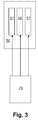
- Figure 3 illustrates an exemplary controller for controlling each of three systems, in accordance with an embodiment.
- the disclosed embodiments seek to improve upon existing polarization pulse shapers by providing full amplitude, phase and polarization control over the frequency components of the pulse, for a single pulse without requiring separating the pulse along multiple paths and addressing different areas of a spatial light modulator. This allows for more compact packaging and more stable configurations and could reduce alignment error.
- a spatial light modulator may be positioned at the Fourier plane of a dispersive optical delay line that includes several arrays of individually addressable liquid crystal light modulator elements, combined with several linear polarizers and quarter-wave retardance waveplates.
- the input pulse may separated into frequency components by the input dispersive element, which are focused at the Fourier plane of the optical delay line.
- the spatial light modulator under electronic control then modifies the retardance of the liquid crystal array elements to control the amplitude, phase and polarization state of the frequency components passing through them. These components are subsequently recombined on the output dispersive elements to form an optical pulse with synthesized amplitude, phase and polarization characteristics.
- the embodiments disclosed herein may be used for modulating pixelated arrays, as well as non-pixelated arrays. See, e.g., C. Dorrer et al. "Programmable phase control of femtosecond pulses by use of a nonpilxelated spatial light modulator," Opt. Lett. Vol. 23, No. 9, pp. 709-711 (1998 ), herein incorporated by reference in its entirety.
- Figure 1 illustrates an exemplary embodiment of a pulse shaper, in which incoming light 10 is input to optical delay line 20.
- Optical delay line 20 generally includes a pair of dispersive element 30, 30', a pair of focusing element 40, 40', and a spatial light modulator 50 located at the Fourier plane F and which can be used to independently control and modulate the each of the phase, amplitude or polarization ellipticity of the pulse.
- Modulated outgoing light 60 may be output from optical delay line 20.
- Dispersive element 30 is configured to resolve incoming light 10 into different constituent wavelength components which are subsequently focused via first focusing element 40 through spatial light modulator 50.
- the spatially modulated light emerging from spatial light modulator 50 is focused by second focusing element 40' onto second dispersive element 30' to reform coherent outgoing light 60.
- Each of dispersive elements 30, 30' may include a diffractive grating, a holographic grating, a ruled grating, a prism or the like, which is configured to resolve incoming light into its various constituent components.
- one or more of dispersive element 30, 30' may be moveable by a motor or actuator so as to control the dispersion of light reflected from the dispersive elements 30, 30'.
- dispersive elements 30, 30' may be transparent or reflective.
- Focusing elements 40, 40' may be conventional lens elements located in a Fourier plane F of dispersive elements 30, 30' respectively.
- First focusing element 40 focuses the incoming light rays at spatial light modulator 50.
- Second focusing element 40' focuses the modulated light rays onto second dispersive element 40'.
- Focusing elements 40, 40' may also include mirror elements.
- the pulse shaper may include more than one pair of focusing elements, such as an 8F or 12F system (still using 2 grating), where systems 51, 55, 57 are positioned in between their own pair of focusing elements, in a serial manner.
- Figure 2 illustrates a cross-sectional view of an exemplary spatial light modulator 50, in accordance with an embodiment in which spatial light modulator 50 generally includes three systems 51, 55, 57. It will be appreciated that the order of the three systems shown in Figure 2 is exemplary, and not to be construed as limiting. Other orders of the systems are possible.
- Spatial light modulator 50 may be located at a Fourier plane F of focusing element 40, 40', as shown in Figure 1 . While Figure 2 shows spaces between the system 51, 55, 57, it will be appreciated that these elements may be substantially formed together.
- Each of systems 51, 55, 57 may include an array of individually addressable light modulating elements under electronic control, such as liquid crystal displays (LCD).
- LCD liquid crystal displays
- First system 51 may include a spectral amplitude modulator device configured to modulate an amplitude of the optical pulse.
- single layer liquid crystal element array 52 may be placed between first and second linear polarizers 53, 53'.
- Liquid crystal array 52 may be configured such that the variable index axes is at approximately 45 degrees to the acceptance orientation of first linear polarizer 53. In accordance with an embodiment, controlling the index of refraction on the variable axes allows for amplitude modulation.
- Second system 55 is a spectral phase and polarization ellipticity modulator.
- a dual layer liquid crystal element array 56 is provided.
- the variable index axis of a first layer of the dual layer liquid crystal element may be located at approximately 45 degrees to the input polarization into the array and a second layer of the dual layer liquid crystal element array may have its variable index axis oriented substantially orthogonal to the first layer.
- dual layer liquid crystal element array 56 is configured to control both the relative phase of the light passing through a single element as well as the polarization ellipticity.
- Third system 57 is a spectral polarization rotator configured to adjust the linear polarization of the optical pulse.
- a single layer liquid crystal element array 58 may be placed between first and second quarter-wave retardance waveplates 59, 59'.
- First waveplate 59 may have its fast axis parallel to the second polarizer 53 in the spectral amplitude modulator.
- the single layer liquid crystal element array 58 may be configured to have its variable axis rotated approximately 45 degrees from the fast axis of the first waveplate 59.
- Second waveplate 59' may have its fast axis oriented substantially orthogonal to the fast axis of first waveplate 59.
- Figure 3 illustrates an exemplary controller 70 for controlling each of three systems 51, 55, 57, in accordance with an embodiment.
- spatial light modulator 50 may be used to modify an amplitude, a phase and a polarization of an optical pulse.
- controller 70 may be dedicated hardware like Application Specific Integrated Circuits (ASIC) or Field Programmable Gate Arrays (FPGA), software (firmware), or a combination of dedicated hardware and software.
- ASIC Application Specific Integrated Circuits
- FPGA Field Programmable Gate Arrays
- firmware software
- the programming and/or configuration may vary.
- Controller 70 may use known methodologies to control each of the amplitude, phase and polarization ellipticity.
Landscapes
- Physics & Mathematics (AREA)
- Electromagnetism (AREA)
- Engineering & Computer Science (AREA)
- Plasma & Fusion (AREA)
- Optics & Photonics (AREA)
- Liquid Crystal (AREA)
- Optical Modulation, Optical Deflection, Nonlinear Optics, Optical Demodulation, Optical Logic Elements (AREA)
Abstract
Description
- The application generally relates to temporal shaping and polarization state modification of ultrashort optical pulses.
- The temporal shaping of ultrafast pulses is a field that has seen considerable growth alongside the development of ultrafast laser pulse sources since the 1980s. A conventional apparatus for ultrafast pulse shaping is a Fourier-domain pulse shaper, which performs a real space Fourier-transform on an input pulse, allowing for modification of the frequency components of the pulse. A variety of modulators can be placed at the Fourier plane of the pulse shaper, including liquid crystal arrays.
- A conventional approach to building an optical delay line for frequency-domain pulse shaping is to use diffraction gratings as the dispersive elements and transmissive lenses as the focusing optics. They are then put into the "zero-dispersion" pulse compressor configuration, resulting in a Fourier plane between the two focusing elements where the frequency components of the input pulse are resolved, and then modulated. However, this approach only permits controlling frequency on a pulse-by-pulse basis.
- Single layer liquid crystal arrays placed at the Fourier plane have been used to modulate the phase of the frequency components of a pulse, or be used to modulate the amplitude of the pulse. In addition, it is known to place dual layer liquid crystal arrays at the Fourier plane to modulate the phase, amplitude or polarization ellipticity of the pulse.
- However, to control the full spectral amplitude, phase and polarization control using a single Fourier-domain pulse shaper requires dividing the input pulse into multiple paths and configuring the pulse shaper such that they address different portions of the spatial light modulator.
- According to an embodiment, an optical pulse shaper includes an optical delay line; a spatial light modulator placed at the Fourier plane of the optical delay line having a spectral amplitude spatial light modulator; a spectral phase and polarization ellipticity spatial light modulator; and a spectral polarization rotator; and a controller configured to independently control an amplitude, a phase and a polarization of an optical pulse.
- According to an aspect of an embodiment, a method for shaping an optical pulse includes independently controlling an amplitude, a phase and a polarization of an optical pulse using the above-described optical pulse shaper.
- Other features and advantages of one or more embodiments of the present application will seem apparent from the following detailed description, and accompanying drawings, and the appended claims.
- Embodiments of the present application will now be disclosed, by way of example only, with reference to the accompanying schematic drawings in which corresponding reference symbols indicate corresponding parts, in which:
-
Figure 1 illustrates an exemplary embodiment of a pulse shaper, in accordance with an embodiment; -
Figure 2 illustrates a cross-sectional view of an exemplary spatial light modulator, in accordance with an embodiment; and -
Figure 3 illustrates an exemplary controller for controlling each of three systems, in accordance with an embodiment. - The disclosed embodiments seek to improve upon existing polarization pulse shapers by providing full amplitude, phase and polarization control over the frequency components of the pulse, for a single pulse without requiring separating the pulse along multiple paths and addressing different areas of a spatial light modulator. This allows for more compact packaging and more stable configurations and could reduce alignment error.
- According to one or more embodiments, a spatial light modulator may be positioned at the Fourier plane of a dispersive optical delay line that includes several arrays of individually addressable liquid crystal light modulator elements, combined with several linear polarizers and quarter-wave retardance waveplates. The input pulse may separated into frequency components by the input dispersive element, which are focused at the Fourier plane of the optical delay line. The spatial light modulator, under electronic control then modifies the retardance of the liquid crystal array elements to control the amplitude, phase and polarization state of the frequency components passing through them. These components are subsequently recombined on the output dispersive elements to form an optical pulse with synthesized amplitude, phase and polarization characteristics.
- The embodiments disclosed herein may be used for modulating pixelated arrays, as well as non-pixelated arrays. See, e.g., C. Dorrer et al. "Programmable phase control of femtosecond pulses by use of a nonpilxelated spatial light modulator," Opt. Lett. Vol. 23, No. 9, pp. 709-711 (1998), herein incorporated by reference in its entirety.
-
Figure 1 illustrates an exemplary embodiment of a pulse shaper, in whichincoming light 10 is input tooptical delay line 20.Optical delay line 20 generally includes a pair ofdispersive element 30, 30', a pair of focusingelement 40, 40', and aspatial light modulator 50 located at the Fourier plane F and which can be used to independently control and modulate the each of the phase, amplitude or polarization ellipticity of the pulse. Modulatedoutgoing light 60 may be output fromoptical delay line 20. -
Dispersive element 30 is configured to resolveincoming light 10 into different constituent wavelength components which are subsequently focused via first focusingelement 40 throughspatial light modulator 50. The spatially modulated light emerging fromspatial light modulator 50 is focused by second focusing element 40' onto second dispersive element 30' to reform coherentoutgoing light 60. - Each of
dispersive elements 30, 30' may include a diffractive grating, a holographic grating, a ruled grating, a prism or the like, which is configured to resolve incoming light into its various constituent components. In addition, one or more ofdispersive element 30, 30' may be moveable by a motor or actuator so as to control the dispersion of light reflected from thedispersive elements 30, 30'. In some implementations,dispersive elements 30, 30' may be transparent or reflective. - Focusing
elements 40, 40' may be conventional lens elements located in a Fourier plane F ofdispersive elements 30, 30' respectively. First focusingelement 40 focuses the incoming light rays atspatial light modulator 50. Second focusing element 40' focuses the modulated light rays onto second dispersive element 40'. Focusingelements 40, 40' may also include mirror elements. In some implementations, the pulse shaper may include more than one pair of focusing elements, such as an 8F or 12F system (still using 2 grating), wheresystems -
Figure 2 illustrates a cross-sectional view of an exemplaryspatial light modulator 50, in accordance with an embodiment in whichspatial light modulator 50 generally includes threesystems Figure 2 is exemplary, and not to be construed as limiting. Other orders of the systems are possible. -
Spatial light modulator 50 may be located at a Fourier plane F of focusingelement 40, 40', as shown inFigure 1 . WhileFigure 2 shows spaces between thesystem systems -
First system 51 may include a spectral amplitude modulator device configured to modulate an amplitude of the optical pulse. In one implementation, single layer liquidcrystal element array 52 may be placed between first and secondlinear polarizers 53, 53'.Liquid crystal array 52 may be configured such that the variable index axes is at approximately 45 degrees to the acceptance orientation of firstlinear polarizer 53. In accordance with an embodiment, controlling the index of refraction on the variable axes allows for amplitude modulation. -
Second system 55 is a spectral phase and polarization ellipticity modulator. In one implementation, a dual layer liquidcrystal element array 56 is provided. For example, the variable index axis of a first layer of the dual layer liquid crystal element may be located at approximately 45 degrees to the input polarization into the array and a second layer of the dual layer liquid crystal element array may have its variable index axis oriented substantially orthogonal to the first layer. In this configuration, dual layer liquidcrystal element array 56 is configured to control both the relative phase of the light passing through a single element as well as the polarization ellipticity. -
Third system 57 is a spectral polarization rotator configured to adjust the linear polarization of the optical pulse. In one implementation, a single layer liquidcrystal element array 58 may be placed between first and second quarter-wave retardance waveplates 59, 59'.First waveplate 59 may have its fast axis parallel to thesecond polarizer 53 in the spectral amplitude modulator. In addition, the single layer liquidcrystal element array 58 may be configured to have its variable axis rotated approximately 45 degrees from the fast axis of thefirst waveplate 59. Second waveplate 59' may have its fast axis oriented substantially orthogonal to the fast axis offirst waveplate 59. -
Figure 3 illustrates anexemplary controller 70 for controlling each of threesystems - Accordingly,
spatial light modulator 50 may be used to modify an amplitude, a phase and a polarization of an optical pulse. - In one or more implementations,
controller 70 may be dedicated hardware like Application Specific Integrated Circuits (ASIC) or Field Programmable Gate Arrays (FPGA), software (firmware), or a combination of dedicated hardware and software. For the different applications of the embodiments disclosed herein, the programming and/or configuration may vary. - Furthermore, according to the various embodiments disclosed in this application, the amplitude, the phase and the polarization of an optical pulse may be selectively modified independently for each pulse, in contrast to conventional approaches described above.
Controller 70 may use known methodologies to control each of the amplitude, phase and polarization ellipticity. - While this disclosure has been described in connection with what is presently considered to be the most practical embodiments, it is to be understood that it is capable of further modifications and is not to be limited to the disclosed embodiments, and this application is intended to cover any variations, uses, equivalent arrangements or adaptations of the disclosure following, in general, the principles of the disclosure and including such departures from the present disclosure as come within known or customary practice in the art to which the application pertains, and as may be applied to the essential features hereinbefore set forth and followed in the spirit and scope of the appended claims.
Claims (20)
- An optical pulse shaper comprising:- an optical delay line;- a spatial light modulator placed at a Fourier plane of the optical delay line, the spatial light modulator comprising:o a spectral amplitude spatial light modulator,o a spectral phase and polarization ellipticity spatial light modulator, ando a spectral polarization rotator; ando a controller configured to independently control an amplitude, a phase and a polarization of an optical pulse.
- The optical pulse shaper accordingly to claim 1, wherein the spectral amplitude spatial light modulator comprises an array of individually addressable light modulating elements and first and second linear polarizers, the array being located between the first and second linear polarizers.
- The optical pulse shaper accordingly to claim 1, wherein the spectral phase and the polarization ellipticity spatial light modulator each comprise an array of individually addressable light modulating elements.
- The optical pulse shaper accordingly to claim 1, wherein the spectral polarization rotator comprises an array of individually addressable light modulating elements and first and second quarter-wave waveplates, the array being located between the first and second quarter-wave waveplates.
- The optical pulse shaper according to claim 1, further comprising a pair of dispersive elements arranged to resolve incoming light into different constituent wavelength components onto to the spatial light modulator to reform coherent outgoing light therefrom.
- The optical pulse shaper according to claim 5, wherein at least one of the dispersive elements comprises a holographic grating.
- The optical pulse shaper according to claim 5, wherein at least one of the dispersive elements comprises a ruled grating.
- The optical pulse shaper according to claim 5, wherein at least one of the dispersive elements comprises a prism.
- The optical pulse shaper according to claim 5, wherein at least one of the dispersive elements is moveable relative to the spatial light modulator.
- The optical pulse shaper according to claim 1, further comprising a pair of focusing elements.
- The optical pulse shaper according to claim 10, wherein at least one of the focusing elements comprises a lens.
- The optical pulse shaper according to claim 10, wherein at least one of the focusing elements comprises a mirror.
- The optical pulse shaper according to claim 2, wherein the array of individually addressable light modulating elements comprises a single layer liquid crystal array.
- The optical pulse shaper according to claim 3, wherein the array of individually addressable light modulating elements comprises a dual layer liquid crystal array.
- The optical pulse shaper according to claim 14, wherein a variable index axis of a first layer of the dual layer liquid crystal array is oriented at approximately 45 degrees to an input polarization into the array, and a variable index axis of a second layer of the dual layer liquid crystal element array is oriented substantially orthogonal to the variable index axis of the first layer.
- The optical pulse shaper according to claim 4, wherein the array of individually addressable light modulating elements comprises a single layer liquid crystal array.
- The optical pulse shaper according to claim 16, wherein a fast axis of the first waveplate is oriented parallel to an output polarizer in the spectral amplitude modulator.
- The optical pulse shaper according to claim 16, wherein a variable axis of the single layer liquid crystal element array is rotated approximately 45 degrees from a fast axis of the first waveplate, and a fast axis of the second waveplate is oriented substantially orthogonal to the fast axis of first waveplate.
- A method for shaping an optical pulse, comprising:Independently controlling an amplitude, a phase and a polarization of an optical pulse using the optical pulse shaper of claim 1.
- The method according to claim 19, further comprising:modulating pixelated arrays or non-pixelated arrays.
Applications Claiming Priority (1)
| Application Number | Priority Date | Filing Date | Title |
|---|---|---|---|
| US12/487,182 US8223298B2 (en) | 2009-06-18 | 2009-06-18 | LCD based polarization, phase and amplitude spatial light modulator |
Publications (3)
| Publication Number | Publication Date |
|---|---|
| EP2264839A2 true EP2264839A2 (en) | 2010-12-22 |
| EP2264839A3 EP2264839A3 (en) | 2014-05-07 |
| EP2264839B1 EP2264839B1 (en) | 2017-10-04 |
Family
ID=42829896
Family Applications (1)
| Application Number | Title | Priority Date | Filing Date |
|---|---|---|---|
| EP10152967.5A Active EP2264839B1 (en) | 2009-06-18 | 2010-02-08 | LCD based polarization, phase and amplitude spatial light modulator. |
Country Status (2)
| Country | Link |
|---|---|
| US (1) | US8223298B2 (en) |
| EP (1) | EP2264839B1 (en) |
Cited By (7)
| Publication number | Priority date | Publication date | Assignee | Title |
|---|---|---|---|---|
| CN104777612A (en) * | 2015-04-28 | 2015-07-15 | 中南大学 | Iterative algorithm for performing shaping on amplitude and phase of light beam simultaneously |
| CN107942598A (en) * | 2017-11-21 | 2018-04-20 | 中国工程物理研究院上海激光等离子体研究所 | Sub- femtosecond ultrashort pulse synthetic method is realized based on Cerenkov radiation |
| US10181336B1 (en) | 2017-08-08 | 2019-01-15 | Microsoft Technology Licensing, Llc | Multi-beam optical system for fast writing of data on glass |
| US10236027B1 (en) | 2018-02-12 | 2019-03-19 | Microsoft Technology Licensing, Llc | Data storage using light of spatially modulated phase and polarization |
| US10248081B2 (en) | 2017-03-10 | 2019-04-02 | Microsoft Technology Licensing, Llc | Holographic phase and amplitude spatial light modulation |
| CN111025665A (en) * | 2019-12-29 | 2020-04-17 | 中国科学院西安光学精密机械研究所 | a time shaper |
| US10809529B2 (en) | 2017-06-15 | 2020-10-20 | Microsoft Technology Licensing, Llc | Optical device having multiplexed electrodes |
Families Citing this family (8)
| Publication number | Priority date | Publication date | Assignee | Title |
|---|---|---|---|---|
| CN103645562B (en) * | 2013-12-20 | 2015-10-21 | 中南大学 | The beam shaping method of modulated amplitude and phase place while of a kind of |
| KR101803320B1 (en) * | 2014-05-12 | 2017-12-05 | 한국전자통신연구원 | Method for fabricating complex spatial light modulator |
| US10267997B2 (en) | 2015-11-11 | 2019-04-23 | Raytheon Company | Infrared scene projector with per-pixel spectral and polarisation capability |
| JP6659339B2 (en) * | 2015-12-11 | 2020-03-04 | 浜松ホトニクス株式会社 | Pulse light generation device and pulse light generation method |
| WO2017169788A1 (en) * | 2016-03-30 | 2017-10-05 | 浜松ホトニクス株式会社 | Pulse light generation device, light irradiation device, optical processing device, optical response measurement device, microscope device, and pulse light generation method |
| JP6654948B2 (en) * | 2016-03-30 | 2020-02-26 | 浜松ホトニクス株式会社 | Method and apparatus for measuring pulse light waveform |
| CN111668693B (en) * | 2020-06-19 | 2021-03-12 | 北京理工大学 | Laser array light source based on liquid crystal geometric phase modulation |
| CN114077076B (en) * | 2021-11-25 | 2023-07-14 | 京东方科技集团股份有限公司 | A display module and a display device |
Family Cites Families (3)
| Publication number | Priority date | Publication date | Assignee | Title |
|---|---|---|---|---|
| WO2001025849A2 (en) * | 1999-09-23 | 2001-04-12 | Purdue Research Foundation | Direct space-to-time pulse shaper and optical pulse train generator |
| DE102006029035B4 (en) * | 2006-06-15 | 2009-10-15 | Freie Universität Berlin | Apparatus and method for the production and detection in amplitude, phase and polarization of shaped laser pulses |
| US7576907B1 (en) * | 2008-05-12 | 2009-08-18 | Colorado State University Research Foundation | Phase and amplitude light pulse shaping using a one-dimensional phase mask |
-
2009
- 2009-06-18 US US12/487,182 patent/US8223298B2/en active Active
-
2010
- 2010-02-08 EP EP10152967.5A patent/EP2264839B1/en active Active
Non-Patent Citations (1)
| Title |
|---|
| C. DORRER ET AL.: "Programmable phase control of femtosecond pulses by use of a nonpilxelated spatial light modulator", OPT. LETT., vol. 23, no. 9, 1998, pages 709 - 711 |
Cited By (8)
| Publication number | Priority date | Publication date | Assignee | Title |
|---|---|---|---|---|
| CN104777612A (en) * | 2015-04-28 | 2015-07-15 | 中南大学 | Iterative algorithm for performing shaping on amplitude and phase of light beam simultaneously |
| US10248081B2 (en) | 2017-03-10 | 2019-04-02 | Microsoft Technology Licensing, Llc | Holographic phase and amplitude spatial light modulation |
| US10809529B2 (en) | 2017-06-15 | 2020-10-20 | Microsoft Technology Licensing, Llc | Optical device having multiplexed electrodes |
| US10181336B1 (en) | 2017-08-08 | 2019-01-15 | Microsoft Technology Licensing, Llc | Multi-beam optical system for fast writing of data on glass |
| CN107942598A (en) * | 2017-11-21 | 2018-04-20 | 中国工程物理研究院上海激光等离子体研究所 | Sub- femtosecond ultrashort pulse synthetic method is realized based on Cerenkov radiation |
| US10236027B1 (en) | 2018-02-12 | 2019-03-19 | Microsoft Technology Licensing, Llc | Data storage using light of spatially modulated phase and polarization |
| CN111025665A (en) * | 2019-12-29 | 2020-04-17 | 中国科学院西安光学精密机械研究所 | a time shaper |
| CN111025665B (en) * | 2019-12-29 | 2020-11-03 | 中国科学院西安光学精密机械研究所 | a time shaper |
Also Published As
| Publication number | Publication date |
|---|---|
| US8223298B2 (en) | 2012-07-17 |
| US20100321615A1 (en) | 2010-12-23 |
| EP2264839A3 (en) | 2014-05-07 |
| EP2264839B1 (en) | 2017-10-04 |
Similar Documents
| Publication | Publication Date | Title |
|---|---|---|
| US8223298B2 (en) | LCD based polarization, phase and amplitude spatial light modulator | |
| TWI839351B (en) | Display device | |
| US10422508B2 (en) | System and method for spectral tuning of broadband light sources | |
| KR102635809B1 (en) | Device for combining light beams which interact with adjacently arranged pixels of a light modulator | |
| US10191191B2 (en) | Diffractive waveplate lenses and applications | |
| EP3161529B1 (en) | Optical system with volume hologram for optic illumination | |
| JP6689186B2 (en) | Polarization conversion system and manufacturing method thereof | |
| EP2159625B1 (en) | Optical waveform shaping device | |
| CN101681030B (en) | Optical waveform shaping device | |
| WO2013140159A1 (en) | Adaptive optics for combined pulse front and phase front control | |
| CN104641286A (en) | Wavelength conversion-type spatial light modulation device | |
| CN210090832U (en) | Laser beam splitting and independent output control device | |
| US8223810B2 (en) | Method and system for generating laser pulses | |
| US8089676B2 (en) | Optical device, ophthalmic lens and device for correcting long-sightedness | |
| CN113687518B (en) | Optical system and optical apparatus | |
| US6947193B1 (en) | Optical phase modulator | |
| US20190391460A1 (en) | Optical assembly and method for influencing the beam direction of at least one light beam | |
| US9575464B2 (en) | Non-mechanical digital/holographic wide angle control of one or more lasers beams | |
| US20230090419A1 (en) | Apparatus and method for recording a holographic optical element | |
| US7564509B2 (en) | Illumination of objects using spatial light modulators | |
| CN102722024A (en) | Light tunable filtering device and method | |
| CN121690387A (en) | Dispersion compensator and dispersion compensation method | |
| Cai et al. | Liquid crystal adaptive optics system for unpolarized light | |
| CN120703996A (en) | Tunable optical filters based on liquid crystal flat panel elements | |
| Stockley et al. | Broadband phase-modulating system for white-light Fourier transformations |
Legal Events
| Date | Code | Title | Description |
|---|---|---|---|
| PUAI | Public reference made under article 153(3) epc to a published international application that has entered the european phase |
Free format text: ORIGINAL CODE: 0009012 |
|
| AK | Designated contracting states |
Kind code of ref document: A2 Designated state(s): AT BE BG CH CY CZ DE DK EE ES FI FR GB GR HR HU IE IS IT LI LT LU LV MC MK MT NL NO PL PT RO SE SI SK SM TR |
|
| AX | Request for extension of the european patent |
Extension state: AL BA RS |
|
| PUAL | Search report despatched |
Free format text: ORIGINAL CODE: 0009013 |
|
| AK | Designated contracting states |
Kind code of ref document: A3 Designated state(s): AT BE BG CH CY CZ DE DK EE ES FI FR GB GR HR HU IE IS IT LI LT LU LV MC MK MT NL NO PL PT RO SE SI SK SM TR |
|
| AX | Request for extension of the european patent |
Extension state: AL BA RS |
|
| RIC1 | Information provided on ipc code assigned before grant |
Ipc: H01S 3/00 20060101AFI20140403BHEP Ipc: G02F 1/1347 20060101ALI20140403BHEP Ipc: G02F 1/13 20060101ALI20140403BHEP Ipc: G02B 27/10 20060101ALI20140403BHEP Ipc: G01J 3/12 20060101ALI20140403BHEP Ipc: G02B 26/06 20060101ALI20140403BHEP Ipc: G01J 3/02 20060101ALI20140403BHEP Ipc: G02F 1/01 20060101ALI20140403BHEP Ipc: G01J 3/10 20060101ALI20140403BHEP |
|
| 17P | Request for examination filed |
Effective date: 20141030 |
|
| RBV | Designated contracting states (corrected) |
Designated state(s): AT BE BG CH CY CZ DE DK EE ES FI FR GB GR HR HU IE IS IT LI LT LU LV MC MK MT NL NO PL PT RO SE SI SK SM TR |
|
| GRAP | Despatch of communication of intention to grant a patent |
Free format text: ORIGINAL CODE: EPIDOSNIGR1 |
|
| RIC1 | Information provided on ipc code assigned before grant |
Ipc: G01J 11/00 20060101ALI20170322BHEP Ipc: G02B 27/10 20060101ALI20170322BHEP Ipc: G02F 1/01 20060101ALI20170322BHEP Ipc: H01S 3/00 20060101AFI20170322BHEP Ipc: G01J 3/10 20060101ALI20170322BHEP Ipc: G02B 26/06 20060101ALI20170322BHEP Ipc: G02F 1/13 20060101ALI20170322BHEP Ipc: G01J 3/12 20060101ALI20170322BHEP Ipc: G02F 1/1347 20060101ALI20170322BHEP Ipc: G01J 3/02 20060101ALI20170322BHEP |
|
| INTG | Intention to grant announced |
Effective date: 20170418 |
|
| GRAS | Grant fee paid |
Free format text: ORIGINAL CODE: EPIDOSNIGR3 |
|
| GRAA | (expected) grant |
Free format text: ORIGINAL CODE: 0009210 |
|
| AK | Designated contracting states |
Kind code of ref document: B1 Designated state(s): AT BE BG CH CY CZ DE DK EE ES FI FR GB GR HR HU IE IS IT LI LT LU LV MC MK MT NL NO PL PT RO SE SI SK SM TR |
|
| REG | Reference to a national code |
Ref country code: GB Ref legal event code: FG4D |
|
| REG | Reference to a national code |
Ref country code: CH Ref legal event code: EP |
|
| REG | Reference to a national code |
Ref country code: AT Ref legal event code: REF Ref document number: 934840 Country of ref document: AT Kind code of ref document: T Effective date: 20171015 |
|
| REG | Reference to a national code |
Ref country code: IE Ref legal event code: FG4D |
|
| REG | Reference to a national code |
Ref country code: DE Ref legal event code: R096 Ref document number: 602010045683 Country of ref document: DE |
|
| REG | Reference to a national code |
Ref country code: FR Ref legal event code: PLFP Year of fee payment: 9 |
|
| REG | Reference to a national code |
Ref country code: NL Ref legal event code: MP Effective date: 20171004 |
|
| REG | Reference to a national code |
Ref country code: LT Ref legal event code: MG4D |
|
| REG | Reference to a national code |
Ref country code: AT Ref legal event code: MK05 Ref document number: 934840 Country of ref document: AT Kind code of ref document: T Effective date: 20171004 |
|
| PG25 | Lapsed in a contracting state [announced via postgrant information from national office to epo] |
Ref country code: NL Free format text: LAPSE BECAUSE OF FAILURE TO SUBMIT A TRANSLATION OF THE DESCRIPTION OR TO PAY THE FEE WITHIN THE PRESCRIBED TIME-LIMIT Effective date: 20171004 |
|
| PG25 | Lapsed in a contracting state [announced via postgrant information from national office to epo] |
Ref country code: ES Free format text: LAPSE BECAUSE OF FAILURE TO SUBMIT A TRANSLATION OF THE DESCRIPTION OR TO PAY THE FEE WITHIN THE PRESCRIBED TIME-LIMIT Effective date: 20171004 Ref country code: SE Free format text: LAPSE BECAUSE OF FAILURE TO SUBMIT A TRANSLATION OF THE DESCRIPTION OR TO PAY THE FEE WITHIN THE PRESCRIBED TIME-LIMIT Effective date: 20171004 Ref country code: FI Free format text: LAPSE BECAUSE OF FAILURE TO SUBMIT A TRANSLATION OF THE DESCRIPTION OR TO PAY THE FEE WITHIN THE PRESCRIBED TIME-LIMIT Effective date: 20171004 Ref country code: NO Free format text: LAPSE BECAUSE OF FAILURE TO SUBMIT A TRANSLATION OF THE DESCRIPTION OR TO PAY THE FEE WITHIN THE PRESCRIBED TIME-LIMIT Effective date: 20180104 Ref country code: LT Free format text: LAPSE BECAUSE OF FAILURE TO SUBMIT A TRANSLATION OF THE DESCRIPTION OR TO PAY THE FEE WITHIN THE PRESCRIBED TIME-LIMIT Effective date: 20171004 |
|
| PG25 | Lapsed in a contracting state [announced via postgrant information from national office to epo] |
Ref country code: HR Free format text: LAPSE BECAUSE OF FAILURE TO SUBMIT A TRANSLATION OF THE DESCRIPTION OR TO PAY THE FEE WITHIN THE PRESCRIBED TIME-LIMIT Effective date: 20171004 Ref country code: LV Free format text: LAPSE BECAUSE OF FAILURE TO SUBMIT A TRANSLATION OF THE DESCRIPTION OR TO PAY THE FEE WITHIN THE PRESCRIBED TIME-LIMIT Effective date: 20171004 Ref country code: AT Free format text: LAPSE BECAUSE OF FAILURE TO SUBMIT A TRANSLATION OF THE DESCRIPTION OR TO PAY THE FEE WITHIN THE PRESCRIBED TIME-LIMIT Effective date: 20171004 Ref country code: IS Free format text: LAPSE BECAUSE OF FAILURE TO SUBMIT A TRANSLATION OF THE DESCRIPTION OR TO PAY THE FEE WITHIN THE PRESCRIBED TIME-LIMIT Effective date: 20180204 Ref country code: BG Free format text: LAPSE BECAUSE OF FAILURE TO SUBMIT A TRANSLATION OF THE DESCRIPTION OR TO PAY THE FEE WITHIN THE PRESCRIBED TIME-LIMIT Effective date: 20180104 Ref country code: GR Free format text: LAPSE BECAUSE OF FAILURE TO SUBMIT A TRANSLATION OF THE DESCRIPTION OR TO PAY THE FEE WITHIN THE PRESCRIBED TIME-LIMIT Effective date: 20180105 |
|
| REG | Reference to a national code |
Ref country code: DE Ref legal event code: R097 Ref document number: 602010045683 Country of ref document: DE |
|
| PG25 | Lapsed in a contracting state [announced via postgrant information from national office to epo] |
Ref country code: DK Free format text: LAPSE BECAUSE OF FAILURE TO SUBMIT A TRANSLATION OF THE DESCRIPTION OR TO PAY THE FEE WITHIN THE PRESCRIBED TIME-LIMIT Effective date: 20171004 Ref country code: CZ Free format text: LAPSE BECAUSE OF FAILURE TO SUBMIT A TRANSLATION OF THE DESCRIPTION OR TO PAY THE FEE WITHIN THE PRESCRIBED TIME-LIMIT Effective date: 20171004 Ref country code: EE Free format text: LAPSE BECAUSE OF FAILURE TO SUBMIT A TRANSLATION OF THE DESCRIPTION OR TO PAY THE FEE WITHIN THE PRESCRIBED TIME-LIMIT Effective date: 20171004 Ref country code: SK Free format text: LAPSE BECAUSE OF FAILURE TO SUBMIT A TRANSLATION OF THE DESCRIPTION OR TO PAY THE FEE WITHIN THE PRESCRIBED TIME-LIMIT Effective date: 20171004 |
|
| PLBE | No opposition filed within time limit |
Free format text: ORIGINAL CODE: 0009261 |
|
| STAA | Information on the status of an ep patent application or granted ep patent |
Free format text: STATUS: NO OPPOSITION FILED WITHIN TIME LIMIT |
|
| PG25 | Lapsed in a contracting state [announced via postgrant information from national office to epo] |
Ref country code: RO Free format text: LAPSE BECAUSE OF FAILURE TO SUBMIT A TRANSLATION OF THE DESCRIPTION OR TO PAY THE FEE WITHIN THE PRESCRIBED TIME-LIMIT Effective date: 20171004 Ref country code: SM Free format text: LAPSE BECAUSE OF FAILURE TO SUBMIT A TRANSLATION OF THE DESCRIPTION OR TO PAY THE FEE WITHIN THE PRESCRIBED TIME-LIMIT Effective date: 20171004 Ref country code: PL Free format text: LAPSE BECAUSE OF FAILURE TO SUBMIT A TRANSLATION OF THE DESCRIPTION OR TO PAY THE FEE WITHIN THE PRESCRIBED TIME-LIMIT Effective date: 20171004 Ref country code: IT Free format text: LAPSE BECAUSE OF FAILURE TO SUBMIT A TRANSLATION OF THE DESCRIPTION OR TO PAY THE FEE WITHIN THE PRESCRIBED TIME-LIMIT Effective date: 20171004 |
|
| 26N | No opposition filed |
Effective date: 20180705 |
|
| REG | Reference to a national code |
Ref country code: CH Ref legal event code: PL |
|
| PG25 | Lapsed in a contracting state [announced via postgrant information from national office to epo] |
Ref country code: MC Free format text: LAPSE BECAUSE OF FAILURE TO SUBMIT A TRANSLATION OF THE DESCRIPTION OR TO PAY THE FEE WITHIN THE PRESCRIBED TIME-LIMIT Effective date: 20171004 |
|
| REG | Reference to a national code |
Ref country code: IE Ref legal event code: MM4A |
|
| REG | Reference to a national code |
Ref country code: BE Ref legal event code: MM Effective date: 20180228 |
|
| PG25 | Lapsed in a contracting state [announced via postgrant information from national office to epo] |
Ref country code: CH Free format text: LAPSE BECAUSE OF NON-PAYMENT OF DUE FEES Effective date: 20180228 Ref country code: SI Free format text: LAPSE BECAUSE OF FAILURE TO SUBMIT A TRANSLATION OF THE DESCRIPTION OR TO PAY THE FEE WITHIN THE PRESCRIBED TIME-LIMIT Effective date: 20171004 Ref country code: LI Free format text: LAPSE BECAUSE OF NON-PAYMENT OF DUE FEES Effective date: 20180228 Ref country code: LU Free format text: LAPSE BECAUSE OF NON-PAYMENT OF DUE FEES Effective date: 20180208 |
|
| PG25 | Lapsed in a contracting state [announced via postgrant information from national office to epo] |
Ref country code: IE Free format text: LAPSE BECAUSE OF NON-PAYMENT OF DUE FEES Effective date: 20180208 |
|
| PG25 | Lapsed in a contracting state [announced via postgrant information from national office to epo] |
Ref country code: BE Free format text: LAPSE BECAUSE OF NON-PAYMENT OF DUE FEES Effective date: 20180228 |
|
| PG25 | Lapsed in a contracting state [announced via postgrant information from national office to epo] |
Ref country code: MT Free format text: LAPSE BECAUSE OF NON-PAYMENT OF DUE FEES Effective date: 20180208 |
|
| PG25 | Lapsed in a contracting state [announced via postgrant information from national office to epo] |
Ref country code: TR Free format text: LAPSE BECAUSE OF FAILURE TO SUBMIT A TRANSLATION OF THE DESCRIPTION OR TO PAY THE FEE WITHIN THE PRESCRIBED TIME-LIMIT Effective date: 20171004 |
|
| PG25 | Lapsed in a contracting state [announced via postgrant information from national office to epo] |
Ref country code: HU Free format text: LAPSE BECAUSE OF FAILURE TO SUBMIT A TRANSLATION OF THE DESCRIPTION OR TO PAY THE FEE WITHIN THE PRESCRIBED TIME-LIMIT; INVALID AB INITIO Effective date: 20100208 Ref country code: PT Free format text: LAPSE BECAUSE OF FAILURE TO SUBMIT A TRANSLATION OF THE DESCRIPTION OR TO PAY THE FEE WITHIN THE PRESCRIBED TIME-LIMIT Effective date: 20171004 |
|
| PG25 | Lapsed in a contracting state [announced via postgrant information from national office to epo] |
Ref country code: MK Free format text: LAPSE BECAUSE OF NON-PAYMENT OF DUE FEES Effective date: 20171004 Ref country code: CY Free format text: LAPSE BECAUSE OF FAILURE TO SUBMIT A TRANSLATION OF THE DESCRIPTION OR TO PAY THE FEE WITHIN THE PRESCRIBED TIME-LIMIT Effective date: 20171004 |
|
| P01 | Opt-out of the competence of the unified patent court (upc) registered |
Effective date: 20230530 |
|
| PGFP | Annual fee paid to national office [announced via postgrant information from national office to epo] |
Ref country code: GB Payment date: 20260122 Year of fee payment: 17 |
|
| PGFP | Annual fee paid to national office [announced via postgrant information from national office to epo] |
Ref country code: DE Payment date: 20260121 Year of fee payment: 17 |
|
| PGFP | Annual fee paid to national office [announced via postgrant information from national office to epo] |
Ref country code: FR Payment date: 20260121 Year of fee payment: 17 |