EP2264753A2 - Integrated device with both SOI insulation and junction insulation and manufacturing method - Google Patents
Integrated device with both SOI insulation and junction insulation and manufacturing method Download PDFInfo
- Publication number
- EP2264753A2 EP2264753A2 EP10183038A EP10183038A EP2264753A2 EP 2264753 A2 EP2264753 A2 EP 2264753A2 EP 10183038 A EP10183038 A EP 10183038A EP 10183038 A EP10183038 A EP 10183038A EP 2264753 A2 EP2264753 A2 EP 2264753A2
- Authority
- EP
- European Patent Office
- Prior art keywords
- layer
- substrate
- insulating
- insulated
- region
- Prior art date
- Legal status (The legal status is an assumption and is not a legal conclusion. Google has not performed a legal analysis and makes no representation as to the accuracy of the status listed.)
- Withdrawn
Links
Images





Classifications
-
- H—ELECTRICITY
- H10—SEMICONDUCTOR DEVICES; ELECTRIC SOLID-STATE DEVICES NOT OTHERWISE PROVIDED FOR
- H10D—INORGANIC ELECTRIC SEMICONDUCTOR DEVICES
- H10D86/00—Integrated devices formed in or on insulating or conducting substrates, e.g. formed in silicon-on-insulator [SOI] substrates or on stainless steel or glass substrates
- H10D86/01—Manufacture or treatment
-
- H—ELECTRICITY
- H10—SEMICONDUCTOR DEVICES; ELECTRIC SOLID-STATE DEVICES NOT OTHERWISE PROVIDED FOR
- H10D—INORGANIC ELECTRIC SEMICONDUCTOR DEVICES
- H10D87/00—Integrated devices comprising both bulk components and either SOI or SOS components on the same substrate
-
- H—ELECTRICITY
- H10—SEMICONDUCTOR DEVICES; ELECTRIC SOLID-STATE DEVICES NOT OTHERWISE PROVIDED FOR
- H10P—GENERIC PROCESSES OR APPARATUS FOR THE MANUFACTURE OR TREATMENT OF DEVICES COVERED BY CLASS H10
- H10P36/00—Gettering within semiconductor bodies
- H10P36/03—Gettering within semiconductor bodies within silicon bodies
- H10P36/07—Gettering within semiconductor bodies within silicon bodies of silicon-on-insulator structures
-
- H—ELECTRICITY
- H10—SEMICONDUCTOR DEVICES; ELECTRIC SOLID-STATE DEVICES NOT OTHERWISE PROVIDED FOR
- H10P—GENERIC PROCESSES OR APPARATUS FOR THE MANUFACTURE OR TREATMENT OF DEVICES COVERED BY CLASS H10
- H10P90/00—Preparation of wafers not covered by a single main group of this subclass, e.g. wafer reinforcement
- H10P90/19—Preparing inhomogeneous wafers
- H10P90/1904—Preparing vertically inhomogeneous wafers
- H10P90/1906—Preparing SOI wafers
-
- H—ELECTRICITY
- H10—SEMICONDUCTOR DEVICES; ELECTRIC SOLID-STATE DEVICES NOT OTHERWISE PROVIDED FOR
- H10W—GENERIC PACKAGES, INTERCONNECTIONS, CONNECTORS OR OTHER CONSTRUCTIONAL DETAILS OF DEVICES COVERED BY CLASS H10
- H10W10/00—Isolation regions in semiconductor bodies between components of integrated devices
- H10W10/01—Manufacture or treatment
- H10W10/061—Manufacture or treatment using SOI processes together with lateral isolation, e.g. combinations of SOI and shallow trench isolations
-
- H—ELECTRICITY
- H10—SEMICONDUCTOR DEVICES; ELECTRIC SOLID-STATE DEVICES NOT OTHERWISE PROVIDED FOR
- H10W—GENERIC PACKAGES, INTERCONNECTIONS, CONNECTORS OR OTHER CONSTRUCTIONAL DETAILS OF DEVICES COVERED BY CLASS H10
- H10W10/00—Isolation regions in semiconductor bodies between components of integrated devices
- H10W10/10—Isolation regions comprising dielectric materials
- H10W10/181—Semiconductor-on-insulator [SOI] isolation regions, e.g. buried oxide regions of SOI wafers
-
- H—ELECTRICITY
- H10—SEMICONDUCTOR DEVICES; ELECTRIC SOLID-STATE DEVICES NOT OTHERWISE PROVIDED FOR
- H10P—GENERIC PROCESSES OR APPARATUS FOR THE MANUFACTURE OR TREATMENT OF DEVICES COVERED BY CLASS H10
- H10P30/00—Ion implantation into wafers, substrates or parts of devices
- H10P30/20—Ion implantation into wafers, substrates or parts of devices into semiconductor materials, e.g. for doping
- H10P30/222—Ion implantation into wafers, substrates or parts of devices into semiconductor materials, e.g. for doping characterised by the angle between the ion beam and the crystal planes or the main crystal surface
Definitions
- the present invention relates to the electronics field. More specifically, the present invention relates to integrated electronic devices of the Silicon On Insulator (SOI) type.
- SOI Silicon On Insulator
- Electronic devices of the SOI type are integrated in a composite wafer, in which a buried insulating layer (such as of silicon oxide) separates two semiconductor layers (such as of mono-crystalline silicon).
- a buried insulating layer such as of silicon oxide
- the lower (thicker) silicon layer defines a common substrate
- the upper (thinner) silicon layer acts as a starting layer, which is grown epitaxially to obtain an active layer housing the different electronic components (such as, MOSFET transistors) of the SOI device.
- the oxide layer provides a robust voltage insulation of the components in the active layer from the substrate.
- DTI Deep Trench Isolation
- processes may be efficiently employed to provide lateral insulation from adjacent components that are integrated in the same SOI device within different insulated regions of the active layer. In particular, such regions are fully insulated by means of the (buried) insulating layer and the DTI trenches.
- standard LOCOS Local Oxidation of Silicon
- STI Shallow Trench Isolation
- the substrate is not directly accessible from the backside of the SOI device it must be biased to the desired voltage through a corresponding contact formed on a front (upper) surface defined by the active layer.
- a typical example is a SOI device that is mounted on a chip carrier with a flip-chip technique, wherein the front surface of the SOI device faces the chip carrier (with its contacts that are directly connected to corresponding bumps of the chip carrier).
- a via hole crossing the insulating layer of the SOI wafer is provided so as to connect the two silicon layers (i.e., the active layer and the substrate).
- the via is formed in a dedicated insulated region of the active layer and is connected to a corresponding contact arranged on the front surface.
- such via is obtained by selectively etching the active layer so forming a trench extending from the front surface down to the substrate.
- the walls of the trench are then covered by a conformal conductive layer (i.e., such as to substantially follow the profile of the underlying structure), which conductive layer further extends on the front surface so as to define the desired contact.
- a drawback of the solution described above is that each trench wastes a significant area of the SOI device.
- the trench must be wide enough to ensure that the conductive layer uniformly covers all its walls so resulting conformal (i.e., the trench has a significant so-called "step coverage”). This significantly increases the size of the whole SOI device.
- a further problem of the SOI wafer is that the active layer can be affected by impurities, which impair the performance of the electronic components that are housed therein (and then of the whole SOI device).
- the SOI wafer is typically used to integrate high-voltage electronic components (e.g., able to sustain voltages ranging from 50V to 250V); however, the same structure is not well suited to house low-voltage electronic components (e.g., able to sustain voltages ranging from 1.8V to 3.3V), for which a standard wafer with PN-junction insulation would be preferred. This problem is particular acute for devices requiring both low-voltage and high-voltage electronic components.
- the present invention is based on idea of providing one or more contact trenches across the insulating layer.
- the present invention provides a solution as set out in the independent claims.
- Advantageous embodiments of the invention are provided in the dependent claims.
- an aspect of the present invention proposes a method for manufacturing an integrated electronic device.
- the method includes the steps of providing an SOI substrate.
- the SOI substrate includes a semiconductor substrate, an insulating layer on the semiconductor substrate, and a semiconductor starting layer on the insulating layer; the substrate and the starting layer are of a first type of conductivity.
- An epitaxial growing process is then performed; the epitaxial growing process is applied to the starting layer to obtain a thicker semiconductor active layer of the first type of conductivity, which embeds the starting layer on the insulating layer.
- At least one insulating trench is formed, extending from an exposed surface of the active layer to the insulating layer; the at least one insulating trench partitions the active layer into insulated regions and at least one further insulated region.
- the method further includes, before the step of performing an epitaxial growing process, forming at least one contact trench extending from an exposed surface of the starting layer to the substrate in correspondence to each further insulated region; each contact trench clears a corresponding portion of the starting layer, of the insulating layer and of the substrate.
- Dopants of a second type of conductivity different from the first type are implanted into at least part of the cleared portions; the epitaxial growing is further applied to the cleared portions thereby at least partially filling each contact trench with semiconductor material; during the epitaxial growing, the dopants diffuse to form an insulating region of the second type of conductivity, which encloses the at least one contact trench of each further insulated region.
- Further components of the device are integrated in each further insulated region; the further components are insulated from the substrate by a junction formed by the corresponding insulating region with the active layer and/or the substrate when reverse-biased.
- Another aspect of the present invention provides a corresponding electronic device.
- the starting material is an SOI substrate 105.
- the SOI substrate includes a semiconductor substrate 110 (for example, of the N-type of conductivity with a resistivity ranging from 1 ⁇ cm to 50 ⁇ cm, such as 40 ⁇ cm).
- the SOI substrate 105 includes a semiconductor starting layer 112 of the N-type, which is separated from the (semiconductor) substrate 110 by an insulating layer 115.
- the insulating layer 115 has a thickness ranging from 0.1 ⁇ m to 2 ⁇ m, and preferably from 0.5 ⁇ m to 1.5 ⁇ m (such as, 1 ⁇ m), whereas the starting layer 112 has a thickness ranging from 50nm to 1.500nm.
- one or more contact trenches 120 are formed by selectively etching the layers 112 and 115.
- a photoresist mask 122 is provided on top of the starting layer 112, so as to leave exposed areas thereof where the contact trenches 120 are desired.
- the layers 112,115 are selectively removed, down to the substrate 110.
- the etching of the layers 112, 115 is performed by two processes, which are substantially anisotropic along a vertical direction Y- perpendicular to the layers 112, 115 (meaning that the layers 112, 115 are etched only vertically).
- the first etching process selectively removes the areas of the starting layer 112 which are left exposed by the photoresist mask 122.
- the second etching process selectively removes the insulating layer 115 in the same areas down to the substrate 110.
- each contact trench 120 clears a corresponding upper portion of the substrate 110 (defining a bottom wall 130b ) and corresponding internal portions of the starting layer 112 and of the insulating layer 115 (defining side walls 130s).
- a dopant implantation is performed in order to form heavily doped internal regions 140 within the substrate 110 and the starting layer 112 (only shown for the substrate 110 in the figure).
- Arsenic (As), Antimony (Sb) or Phosphorus (P) dopant ions are used; preferably, the dopant dose ranges from 10 12 ions/cm 2 to 10 16 ions/cm 2 .
- Such implantation is performed with the photoresist mask 122 still in place, so as to have the internal regions 140 in zones corresponding to the contact trenches 120.
- each implantation process involves the use of a beam of dopant ions propagating along a direction I having a corresponding tilt ⁇ with respect to the vertical direction Y.
- an epitaxial growing process is then carried out (for example, by means of Vapor-Phase Epitaxy).
- the epitaxial growing process is performed in a room comprising a silicon compound (for example, silicon tetrachloride SiCl4 or trichlorosilane SiHCl 3 ) at high temperature (for example, ranging from 1000°C to 1200°C).
- the epitaxial growing process applied to the starting layer 112 results in the generation of an active layer 142 of the N-type (for example, with a thickness of about 1/ ⁇ m-10 ⁇ m).
- the same epitaxial growing process applied to the walls 130b and 130s at least partially fills the contact trenches 120, possibly leaving vacant regions 143 therein.
- This effect is due both to the geometry of the contact trenches 120 and to the different growing rates of the epitaxial growing process over the cleared portions of the substrate 110, of the insulating layer 115 and of the starting layer 112 (shown in Figure 1C ).
- the obtained structure may be not planar, with recesses corresponding to the contact trenches 120 on its front (upper) surface 150.
- the layout of the contact trenches 120 is finely tuned taking into account the epitaxial growing process parameters (as described in detail in the following).
- the dopant ions of the internal regions 140 diffuse thereby forming a contact region 145 of the N+ type.
- the contact region 145 encloses all the contact trenches 120 (across the insulating layer 115 ) so as to electrically couple the substrate 110 with the active layer 142.
- the contact region 145 is more conductive than the semiconductor material surrounding it, due to the high dopant concentration created by the above-mentioned diffusion.
- a field oxide layer 155 is formed (for example, by means of a selective or LOCOS thermal growth) in order to cover the front surface 150 of the active layer 142 - except for a portion thereof where active areas 157 of the desired front-rear contact will be defined.
- a silicon nitride (such as Si 3 N 4 ) mask - not shown in the figure - is provided on top of the active layer 142, so as to leave exposed areas thereof where the field oxide layer 155 is to be grown.
- one or more insulating trenches 158 - for example, of the DTI type - are then formed.
- another photoresist mask 159 is provided on top of the field oxide layer 155 and of the active layer 142, so as to leave exposed areas thereof where the insulating trenches 158 are desired.
- the active layer 142 and the field oxide layer 155 are selectively removed, down to the insulating layer 115.
- the insulating trenches 158 partition the active layer 142 into insulated regions 160, which will be used to integrate the desired electronic components.
- the insulating trench 158 around the contact trenches 120 defines an (insulated) active region 161, which is used to contact the substrate 110 from the front surface 150 so as to provide the desired front-rear contact through the insulating layer 115.
- the mask 159 is stripped away.
- the insulating trench 158 is filled with dielectric material, such as silicon-dioxide (for example, by means of CVD oxide deposition).
- dielectric material such as silicon-dioxide (for example, by means of CVD oxide deposition).
- an implantation process is performed (through the active areas 157 ) in order to obtain a heavily doped region within the active region 161; in the example at issue, As or P dopant ions are used.
- the dopant ions diffuse so forming an N+ contact region 170, which extends from the front surface 150 to the (buried) contact region 145.
- a dielectric layer 175 (for example, doped silicon oxide) is deposited on top of the field oxide layer 155 and on the active areas 157, for example, by means of a CVD process. Then, the dielectric layer 175 is planarized, typically using the CMP (Chemical Mechanical Polishing) technique, so as to flush the recesses corresponding to the contact trenches 120 formed beforehand.
- CMP Chemical Mechanical Polishing
- each contact window 185 is etched in the dielectric layer 175 in correspondence of the active areas 157 (so as to reach the contact region 170 ).
- each contact window 185 surrounds the contact region 145 in plant view.
- each point of the contact window 185 is spaced apart from an axis A of each contact trench 120 (parallel to the vertical direction) in order to prevent any disturbs due to the corresponding recesses on the front surface 150.
- a line B connecting each point of the contact window 185 (at the corresponding active area 157 on the front surface 150 ) with the edge of the contact trench 120 closest to the contact window 185 (on its bottom wall at an upper surface of the substrate 110 ) forms an angle ⁇ , which is higher than 60°, preferably at least equal to 61°-85°, and more preferably at least equal to 64°-82° (such as at least equal to 65°).
- this condition must be satisfied by the internal edge of the contact window 185, with respect to the contact trench 120 that is closest to the contact window 185 (being the same angle higher otherwise).
- a metallization layer 190 (for example, A1 or Ti/TiN plus a W-plug and an A1 layer) is deposited on top of the wafer, thereby filling the contact windows 185 and covering the exposed surface of the dielectric layer 175.
- the metallization layer 190 is then shaped to define a pad.
- the desired electronic device 100 is obtained; the electronic device 100 includes the required front-rear contact, which allows contacting the substrate 110 from the front surface 150 (for example, to bias the substrate 110 at a predetermined voltage in flip-chip applications). More specifically, this front-rear contact is obtained through the pad 190, the contact windows 185 (the higher the number of contact windows 185, the higher the conductivity thereof), the contact region 170, and the contact region 145.
- the front-rear contact described-above has a small size (compared to the solutions known in the art); this has a beneficial effect on the occupation area of the whole electronic device 100. Moreover, this result is achieved without adversely affecting the electrical properties of the front-rear contact, especially its resistance.
- the contact region 145 contributes to the desired characteristics of the front-rear contact.
- a contribution is given by the contact region 145; particularly, its beneficial effect is emphasized by the fact that the contact region 145 surrounds the contact trenches 120. This is achieved thanks to the corresponding implantation processes that are tilted as indicated above (with the best result provided by the proposed angles).
- FIG. 2 a partially cut-away elevation view of the above-described electronic device 100 is shown.
- the insulating trench 158 defines the active region 161 for the front-rear contact.
- the active area 157 for the contact windows within the active region 161 surrounds the contact region 145 around the contact trenches 120.
- each contact trench 120 has a square transversal section with each side (denoted with 1 ) ranging from 1.5 ⁇ m to 5 ⁇ m, and more preferably from 2 ⁇ m to 4 ⁇ m (such as 3 ⁇ m).
- the contact trenches 120 are arranged in a matrix (with three rows and three columns in the example at issue).
- each contact trench 120 is spaced apart from any adjacent contact trench 120 by a distance (denoted with s ), which preferably ranges from 1 ⁇ m to 3 ⁇ m, and more preferably from 1.2 ⁇ m to 2.5 ⁇ m (such as 1.5 ⁇ m).
- the proposed layout of the contact trenches 120 allows reducing the above-mentioned electrical discontinuities of the electronic device 100 (due to the non-planarity caused by the contact trenches 120 ). Moreover, this arrangement of the contact trenches 120 has been found to provide optimum results (in terms of the lowering of the front-rear contact resistance).
- a diagram 300 shows a set of working characteristics of the front-rear contact according to an embodiment of the present invention (depending on the dopant concentration of the semiconductor material surrounding the contact trenches across the insulating layer).
- the diagram 300 has a current I [mA] on a left axis of ordinates, a resistance R [k ⁇ ] on a right axis of ordinates and a biasing voltage V [V] on an axis of abscissas.
- two adjacent front-rear contacts are formed in the same electronic device (both of them connected to its substrate). Biasing voltages V ranging from -5V to 5V are then applied between the two front-rear contacts, and the corresponding currents I are measured (with the resistance R that is calculated accordingly).
- working characteristics 310 (representing the current) and 320 (representing the resistance) are obtained when the front-rear contacts are manufactured as described above.
- the remaining working characteristics 330 (representing the current) and 340 (representing the resistance) are obtained for non-optimized electronic devices without the (more doped) contact region surrounding the contact trenches (i.e., when the manufacturing process of the electronic device does not provide the implantation processes after the etching of the contact trenches).
- the working characteristic 320 is below the working characteristic 340 (meaning that the resistance R of the front-rear contact is lower).
- the resistance R is reduced by about one third (from 15k ⁇ to 6k ⁇ ).
- the contact region 145 acts as a gettering zone for any impurities of the whole active layer 142.
- one or more insulating trenches 405 are formed as described above (so as to reach the insulating layer 115 ).
- the insulating trenches 405 are likewise filled with dielectric material, and the whole front surface 150 is covered with a field oxide layer 410 suitably planarized (so as to obtain the desired electronic device 400 ).
- the field oxide layer 410 covers the whole front surface 150 (without any contact windows); moreover, no additional contact region is formed (from the front surface 150 to the contact region 145 ).
- the insulating trenches 405 again partition the active layer 142 into multiple active regions 415, which will be used to integrate the desired electronic components (schematically represented in the figure as 420 ). Moreover, the insulating trench 405 around the contact trenches 120 defines an (insulated) gettering region 425, which segregates the impurities - gettered by the contact region 145 beforehand.
- the starting material is again an SOI substrate 505 (with a semiconductor substrate 510, a semiconductor starting layer 512, and an insulating layer 115 ).
- the insulating layer 515 has a thickness lower than 0.5 ⁇ m, and preferably ranging from 0.2 ⁇ m to 0.4 ⁇ m (such as 0.3 ⁇ m);
- the semiconductor starting layer 512 has a thickness lower than 0.5 ⁇ m, and preferably ranging from 0.1 ⁇ m to 0.45 ⁇ m (such as 0.3 ⁇ m).
- a single contact trench 520 is formed as above through the layers 512, 515 (by means of two substantially anisotropic etching processes - along a vertical direction Y - through a corresponding photoresist mask 522); the contact trench 520 likewise clears a corresponding front portion of the substrate 510 (defining a bottom wall 530b ) and corresponding internal portions of the starting layer 512 and of the insulating layer 515 (defining side walls 530s).
- the contact trench 520 has preferably a square shape, with each side higher than 400 ⁇ m.
- two (or more) dopant implantation processes are again performed (along directions I titled as above with respect to the vertical direction Y ), in order to form heavily doped internal regions 540 within the substrate 510 and the starting layer 512 (only shown for the substrate 510 in the figure).
- the internal region 540 is of the opposite type of conductivity with respect to the substrate 510 and the starting layer 512 (i.e., of the P-type).
- Boron (B) dopant ions are used; preferably, the dopant dose ranges from 10 12 ions/cm 2 to 10 16 ions/cm 2 .
- the photoresist mask 522 is likewise stripped at the end of the implantation processes.
- a similar epitaxial growing process is carried out so as to form an active layer 542 of the N-type again; at the same time, the epitaxial growing process completely fills the contact trench 520 (without leaving any vacant regions).
- the dopant ions of the internal region 540 diffuse thereby forming an insulating region 545 of the P+ type.
- the insulating region 545 encloses the contact trench 520 (across the insulating layer 515 ) so as to define a PN junction with the substrate 510 and another PN junction with the active layer 542.
- a field oxide layer 555 is again formed on top of the active layer 542 - except for a portion thereof where a (larger) active area 557 around the insulating region 545 is desired.
- one or more insulating trenches 558 are formed as described above reaching the insulating layer 515 (so as to obtain the desired electronic device 500 ).
- the insulating trenches 558 again partition the active layer 542 into multiple active regions 560, which are fully insulated by the insulating layer 515 and the insulating trenches 558.
- the insulating trench 558 shown in the figure - around the contact trench 520 - defines a further active region 561; the active region 561 is insulated from the substrate 510 by means of the PN junctions formed by the insulating region 545 (when reverse-biased).
- the active regions 560 are typically used to integrate high-voltage electronic components or devices that need fast access time, low leakage and low parasitic capacitance (schematically represented in the figure as 580 ), so as to benefit of the typical advantages of the SOI structures.
- the active region 561 is typically used to integrate low-voltage electronic components or devices that have to dissipate heat through the semiconductor substrate (schematically represented in the figure as 581 ), which instead would be adversely affected by the SOI structure.
- the device has an equivalent structure (such as with layers having different thickness); moreover, although in the preceding description reference has been made to a semiconductor substrate and a starting layer of N-type, the conductivity type of these layers may be reversed (i.e., of P-type).
- the starting material may be either a SOI wafer already ready to be processed or a structure formed by conventional manufacturing processes.
- the implantation processes after the epitaxial growing process are not strictly necessary and they may be omitted in a simplified implementation (even if the performance of the resulting structure would be reduced).
- different beams of dopant ions can be used during the implantation processes (even with a different number of them, down to a single one).
- the proposed structures may be part of the design of integrated circuits.
- the design may also be created in a programming language; moreover, if the designer does not fabricate chips or masks, the design may be transmitted by physical means to others.
- the resulting integrated circuits may be distributed by their manufacturer in raw wafer form, as bare dies, or in packages form.
- the devices may be integrated with other circuits in the same chip, or they may be mounted in intermediate products (such as mother boards).
- the integrated circuits are suitable to be used in complex systems (such as computers).
Landscapes
- Element Separation (AREA)
- Thin Film Transistor (AREA)
- Recrystallisation Techniques (AREA)
Abstract
Description
- The present invention relates to the electronics field. More specifically, the present invention relates to integrated electronic devices of the Silicon On Insulator (SOI) type.
- Electronic devices of the SOI type are integrated in a composite wafer, in which a buried insulating layer (such as of silicon oxide) separates two semiconductor layers (such as of mono-crystalline silicon). Particularly, the lower (thicker) silicon layer defines a common substrate; the upper (thinner) silicon layer acts as a starting layer, which is grown epitaxially to obtain an active layer housing the different electronic components (such as, MOSFET transistors) of the SOI device.
- The oxide layer provides a robust voltage insulation of the components in the active layer from the substrate. Moreover, DTI (Deep Trench Isolation) processes may be efficiently employed to provide lateral insulation from adjacent components that are integrated in the same SOI device within different insulated regions of the active layer. In particular, such regions are fully insulated by means of the (buried) insulating layer and the DTI trenches. In addition, standard LOCOS (Local Oxidation of Silicon) or STI (Shallow Trench Isolation) processes may be used to provide a further lateral insulation of the components that are integrated in the same insulated region. Moreover, the SOI devices have other important advantages. For example, they do not suffer leakage effects between adjacent components. Moreover, the parasitic capacitances of the components integrated in the SOI device are significantly reduced.
- Usually it is desired to maintain the substrate at a predetermined voltage (for example, to avoid undesired capacitive coupling effects). Particularly, when the substrate is not directly accessible from the backside of the SOI device it must be biased to the desired voltage through a corresponding contact formed on a front (upper) surface defined by the active layer. A typical example is a SOI device that is mounted on a chip carrier with a flip-chip technique, wherein the front surface of the SOI device faces the chip carrier (with its contacts that are directly connected to corresponding bumps of the chip carrier).
- For this purpose, a via hole (or simply via) crossing the insulating layer of the SOI wafer is provided so as to connect the two silicon layers (i.e., the active layer and the substrate). Typically, the via is formed in a dedicated insulated region of the active layer and is connected to a corresponding contact arranged on the front surface.
- In the state of the art such via is obtained by selectively etching the active layer so forming a trench extending from the front surface down to the substrate. The walls of the trench are then covered by a conformal conductive layer (i.e., such as to substantially follow the profile of the underlying structure), which conductive layer further extends on the front surface so as to define the desired contact.
- A drawback of the solution described above is that each trench wastes a significant area of the SOI device. In fact, the trench must be wide enough to ensure that the conductive layer uniformly covers all its walls so resulting conformal (i.e., the trench has a significant so-called "step coverage"). This significantly increases the size of the whole SOI device.
- A further problem of the SOI wafer is that the active layer can be affected by impurities, which impair the performance of the electronic components that are housed therein (and then of the whole SOI device).
- In addition, the SOI wafer is typically used to integrate high-voltage electronic components (e.g., able to sustain voltages ranging from 50V to 250V); however, the same structure is not well suited to house low-voltage electronic components (e.g., able to sustain voltages ranging from 1.8V to 3.3V), for which a standard wafer with PN-junction insulation would be preferred. This problem is particular acute for devices requiring both low-voltage and high-voltage electronic components.
- In principle, the present invention is based on idea of providing one or more contact trenches across the insulating layer.
- Particularly, the present invention provides a solution as set out in the independent claims. Advantageous embodiments of the invention are provided in the dependent claims.
- In detail, an aspect of the present invention proposes a method for manufacturing an integrated electronic device. The method includes the steps of providing an SOI substrate. The SOI substrate includes a semiconductor substrate, an insulating layer on the semiconductor substrate, and a semiconductor starting layer on the insulating layer; the substrate and the starting layer are of a first type of conductivity. An epitaxial growing process is then performed; the epitaxial growing process is applied to the starting layer to obtain a thicker semiconductor active layer of the first type of conductivity, which embeds the starting layer on the insulating layer. At least one insulating trench is formed, extending from an exposed surface of the active layer to the insulating layer; the at least one insulating trench partitions the active layer into insulated regions and at least one further insulated region. Components of the device are integrated in the insulated regions; the components are insulated from the substrate by the insulating layer. In the solution according to an embodiment of the invention, the method further includes, before the step of performing an epitaxial growing process, forming at least one contact trench extending from an exposed surface of the starting layer to the substrate in correspondence to each further insulated region; each contact trench clears a corresponding portion of the starting layer, of the insulating layer and of the substrate. Dopants of a second type of conductivity different from the first type are implanted into at least part of the cleared portions; the epitaxial growing is further applied to the cleared portions thereby at least partially filling each contact trench with semiconductor material; during the epitaxial growing, the dopants diffuse to form an insulating region of the second type of conductivity, which encloses the at least one contact trench of each further insulated region. Further components of the device are integrated in each further insulated region; the further components are insulated from the substrate by a junction formed by the corresponding insulating region with the active layer and/or the substrate when reverse-biased.
- Another aspect of the present invention provides a corresponding electronic device.
- The present invention, as well as further features and the advantages thereof, will be best understood by reference to the following detailed description, given purely by way of a non-restrictive indication, to be read in conjunction with the accompanying drawings. In this respect, it is expressly intended that the figures are not necessary drawn to scale and that, unless otherwise indicated, they are merely intended to conceptually illustrate the structures and procedures described herein. Particularly:
-
Figures 1A through 1I are cross-section views illustrating the main phases of the manufacturing process of an electronic device, according to a first embodiment of the present invention; -
Figure 2 shows a partially cut-away elevation view of this electronic device; -
Figure 3 shows an exemplificative diagram relating to electrical operative parameters of the same electronic device; -
Figures 4A through 4B are cross-section views illustrating the main phases of the manufacturing process of an electronic device, according to a second embodiment of the present invention; and -
Figures 5A through 5F are cross-section views illustrating the main phases of the manufacturing process of an electronic device, according to a third embodiment of the present invention. - Referring to
Figures 1A through 1I , a process is described for manufacturing an electronic device 100 (seeFigure 1I ) with a front-rear contact according to a first embodiment of the present invention. - Considering in particular
Figure 1A , the starting material is anSOI substrate 105. In detail, the SOI substrate includes a semiconductor substrate 110 (for example, of the N-type of conductivity with a resistivity ranging from 1Ωcm to 50Ωcm, such as 40Ωcm). Moreover, theSOI substrate 105 includes asemiconductor starting layer 112 of the N-type, which is separated from the (semiconductor)substrate 110 by aninsulating layer 115. For example, theinsulating layer 115 has a thickness ranging from 0.1µm to 2µm, and preferably from 0.5µm to 1.5µm (such as, 1µm), whereas thestarting layer 112 has a thickness ranging from 50nm to 1.500nm. - Moving now to
Figure 1B , one or more contact trenches 120 (such as a matrix of 9contact trenches 120, three of which shown in the figure) are formed by selectively etching thelayers photoresist mask 122 is provided on top of thestarting layer 112, so as to leave exposed areas thereof where thecontact trenches 120 are desired. Using suitable etching techniques, the layers 112,115 are selectively removed, down to thesubstrate 110. - In particular, the etching of the
layers layers 112, 115 (meaning that thelayers starting layer 112 which are left exposed by thephotoresist mask 122. Then, the second etching process selectively removes theinsulating layer 115 in the same areas down to thesubstrate 110. - In such a way, each
contact trench 120 clears a corresponding upper portion of the substrate 110 (defining abottom wall 130b) and corresponding internal portions of thestarting layer 112 and of the insulating layer 115 (definingside walls 130s). - As shown in
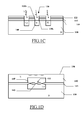
Figure 1C , a dopant implantation is performed in order to form heavily dopedinternal regions 140 within thesubstrate 110 and the starting layer 112 (only shown for thesubstrate 110 in the figure). For example, in order to form N+internal regions 140, Arsenic (As), Antimony (Sb) or Phosphorus (P) dopant ions are used; preferably, the dopant dose ranges from 1012 ions/cm2 to 1016 ions/cm2. Such implantation is performed with thephotoresist mask 122 still in place, so as to have theinternal regions 140 in zones corresponding to thecontact trenches 120. - For this purpose, two (or more) dopant implantation processes are performed along different directions, in order to cause desired dopant ions to penetrate the
sidewalls 130s of the startinglayer 112 and thebottom walls 130b of thesubstrate 110. Particularly, each implantation process involves the use of a beam of dopant ions propagating along a direction I having a corresponding tilt α with respect to the vertical direction Y. Preferably, the tilt α ranges from 2° to 45°, and more preferably from 5° to 20° (such as α = 7°). Preferably, two implantation processes are performed along directions that are symmetric with respect to the vertical direction Y (so as to reach opposed regions). For example, during a first implantation process the wafer is inclined with respect to the direction of the dopant ions beam at an angle α = 7°, whereas during a second implantation process the wafer is inclined at the opposite angle α = -7°. - The
photoresist mask 122 is stripped at the end of the implantation processes. Referring now toFigure 1D , an epitaxial growing process is then carried out (for example, by means of Vapor-Phase Epitaxy). The epitaxial growing process is performed in a room comprising a silicon compound (for example, silicon tetrachloride SiCl4 or trichlorosilane SiHCl3) at high temperature (for example, ranging from 1000°C to 1200°C). The epitaxial growing process applied to the starting layer 112 (shown inFigure 1C ) results in the generation of anactive layer 142 of the N-type (for example, with a thickness of about 1/µm-10µm). - Concurrently, the same epitaxial growing process applied to the
walls Figure 1C ) at least partially fills thecontact trenches 120, possibly leavingvacant regions 143 therein. This effect is due both to the geometry of thecontact trenches 120 and to the different growing rates of the epitaxial growing process over the cleared portions of thesubstrate 110, of the insulatinglayer 115 and of the starting layer 112 (shown inFigure 1C ). As a result, the obtained structure may be not planar, with recesses corresponding to thecontact trenches 120 on its front (upper)surface 150. In order to reduce this non-planarity (which may lead to an electrical discontinuity of the final structure), the layout of thecontact trenches 120 is finely tuned taking into account the epitaxial growing process parameters (as described in detail in the following). - During the epitaxial growing process, the dopant ions of the internal regions 140 (shown in
Figure 1C ) diffuse thereby forming acontact region 145 of the N+ type. As can be noted, thecontact region 145 encloses all the contact trenches 120 (across the insulating layer 115) so as to electrically couple thesubstrate 110 with theactive layer 142. Thecontact region 145 is more conductive than the semiconductor material surrounding it, due to the high dopant concentration created by the above-mentioned diffusion. - Moving to
Figure 1E , afield oxide layer 155 is formed (for example, by means of a selective or LOCOS thermal growth) in order to cover thefront surface 150 of the active layer 142 - except for a portion thereof whereactive areas 157 of the desired front-rear contact will be defined. For this purpose, a silicon nitride (such as Si3N4) mask - not shown in the figure - is provided on top of theactive layer 142, so as to leave exposed areas thereof where thefield oxide layer 155 is to be grown. - Continuing to
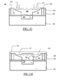
Figure 1F , one or more insulating trenches 158 - for example, of the DTI type - are then formed. For this purpose, anotherphotoresist mask 159 is provided on top of thefield oxide layer 155 and of theactive layer 142, so as to leave exposed areas thereof where the insulatingtrenches 158 are desired. Using suitable etching techniques, theactive layer 142 and thefield oxide layer 155 are selectively removed, down to the insulatinglayer 115. As a result, the insulatingtrenches 158 partition theactive layer 142 intoinsulated regions 160, which will be used to integrate the desired electronic components. Moreover, the insulatingtrench 158 around thecontact trenches 120 defines an (insulated)active region 161, which is used to contact thesubstrate 110 from thefront surface 150 so as to provide the desired front-rear contact through the insulatinglayer 115. - For this purpose, the
mask 159 is stripped away. Continuing toFigure 1G , the insulatingtrench 158 is filled with dielectric material, such as silicon-dioxide (for example, by means of CVD oxide deposition). Thereafter, an implantation process is performed (through the active areas 157) in order to obtain a heavily doped region within theactive region 161; in the example at issue, As or P dopant ions are used. Then, the dopant ions diffuse so forming anN+ contact region 170, which extends from thefront surface 150 to the (buried)contact region 145. - Moving to
Figure 1H , a dielectric layer 175 (for example, doped silicon oxide) is deposited on top of thefield oxide layer 155 and on theactive areas 157, for example, by means of a CVD process. Then, thedielectric layer 175 is planarized, typically using the CMP (Chemical Mechanical Polishing) technique, so as to flush the recesses corresponding to thecontact trenches 120 formed beforehand. - As shown in
Figure 1I , a plurality ofcontact windows 185 are etched in thedielectric layer 175 in correspondence of the active areas 157 (so as to reach the contact region 170). Preferably, eachcontact window 185 surrounds thecontact region 145 in plant view. Particularly, each point of thecontact window 185 is spaced apart from an axis A of each contact trench 120 (parallel to the vertical direction) in order to prevent any disturbs due to the corresponding recesses on thefront surface 150. Preferably, a line B connecting each point of the contact window 185 (at the correspondingactive area 157 on the front surface 150) with the edge of thecontact trench 120 closest to the contact window 185 (on its bottom wall at an upper surface of the substrate 110) forms an angle β, which is higher than 60°, preferably at least equal to 61°-85°, and more preferably at least equal to 64°-82° (such as at least equal to 65°). In other words, this condition must be satisfied by the internal edge of thecontact window 185, with respect to thecontact trench 120 that is closest to the contact window 185 (being the same angle higher otherwise). - Afterwards, a metallization layer 190 (for example, A1 or Ti/TiN plus a W-plug and an A1 layer) is deposited on top of the wafer, thereby filling the
contact windows 185 and covering the exposed surface of thedielectric layer 175. Themetallization layer 190 is then shaped to define a pad. In such a way, the desiredelectronic device 100 is obtained; theelectronic device 100 includes the required front-rear contact, which allows contacting thesubstrate 110 from the front surface 150 (for example, to bias thesubstrate 110 at a predetermined voltage in flip-chip applications). More specifically, this front-rear contact is obtained through thepad 190, the contact windows 185 (the higher the number ofcontact windows 185, the higher the conductivity thereof), thecontact region 170, and thecontact region 145. - The front-rear contact described-above has a small size (compared to the solutions known in the art); this has a beneficial effect on the occupation area of the whole
electronic device 100. Moreover, this result is achieved without adversely affecting the electrical properties of the front-rear contact, especially its resistance. - Particularly, several factors contribute to the desired characteristics of the front-rear contact. For example, a contribution is given by the
contact region 145; particularly, its beneficial effect is emphasized by the fact that thecontact region 145 surrounds thecontact trenches 120. This is achieved thanks to the corresponding implantation processes that are tilted as indicated above (with the best result provided by the proposed angles). - In addition, the choice of displacing the
contact windows 185 with respect to the axis of thecontact trenches 120 creates a preferential path for the electrical charge along which the resistance of the semiconductor material is further reduced (with the best results that are provided by the proposed angles). - Moving to
Figure 2 , a partially cut-away elevation view of the above-describedelectronic device 100 is shown. As can be noted, the insulatingtrench 158 defines theactive region 161 for the front-rear contact. Theactive area 157 for the contact windows within theactive region 161 surrounds thecontact region 145 around thecontact trenches 120. - Preferably, each
contact trench 120 has a square transversal section with each side (denoted with 1) ranging from 1.5µm to 5µm, and more preferably from 2µm to 4µm (such as 3µm). Thecontact trenches 120 are arranged in a matrix (with three rows and three columns in the example at issue). Particularly, eachcontact trench 120 is spaced apart from anyadjacent contact trench 120 by a distance (denoted with s), which preferably ranges from 1µm to 3µm, and more preferably from 1.2µm to 2.5µm (such as 1.5µm). - The proposed layout of the
contact trenches 120 allows reducing the above-mentioned electrical discontinuities of the electronic device 100 (due to the non-planarity caused by the contact trenches 120). Moreover, this arrangement of thecontact trenches 120 has been found to provide optimum results (in terms of the lowering of the front-rear contact resistance). - The above-mentioned advantages of the proposed solution are confirmed by experiment results.
- Particularly referring to
Figure 3 , a diagram 300 shows a set of working characteristics of the front-rear contact according to an embodiment of the present invention (depending on the dopant concentration of the semiconductor material surrounding the contact trenches across the insulating layer). In particular, the diagram 300 has a current I[mA] on a left axis of ordinates, a resistance R[kΩ] on a right axis of ordinates and a biasing voltage V[V] on an axis of abscissas. - For this purpose, two adjacent front-rear contacts are formed in the same electronic device (both of them connected to its substrate). Biasing voltages V ranging from -5V to 5V are then applied between the two front-rear contacts, and the corresponding currents I are measured (with the resistance R that is calculated accordingly).
- As can be seen, working characteristics 310 (representing the current) and 320 (representing the resistance) are obtained when the front-rear contacts are manufactured as described above. The remaining working characteristics 330 (representing the current) and 340 (representing the resistance) are obtained for non-optimized electronic devices without the (more doped) contact region surrounding the contact trenches (i.e., when the manufacturing process of the electronic device does not provide the implantation processes after the etching of the contact trenches).
- As it can be noted, the working
characteristic 320 is below the working characteristic 340 (meaning that the resistance R of the front-rear contact is lower). For example, when the biasing voltage V is equal to 2V the resistance R is reduced by about one third (from 15kΩ to 6kΩ). - With reference now to
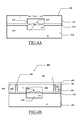
Figures 4A through 4B , a process is described for manufacturing an electronic device 400 (seeFigure 4B ) adapted for gettering of impurities according to a second embodiment of the present invention. - Considering in particular
Figure 4A , the same process steps described above are repeated until the creation of the contact region 145 (the elements corresponding to the ones of the preceding figures are denoted with the same references, and their explanation will be omitted for the sake of simplicity). The contact region acts as a gettering zone for any impurities of the wholeactive layer 142. - Moving now to
Figure 4B , one or more insulatingtrenches 405 are formed as described above (so as to reach the insulating layer 115). The insulatingtrenches 405 are likewise filled with dielectric material, and the wholefront surface 150 is covered with afield oxide layer 410 suitably planarized (so as to obtain the desired electronic device 400). As can be seen, in this case thefield oxide layer 410 covers the whole front surface 150 (without any contact windows); moreover, no additional contact region is formed (from thefront surface 150 to the contact region 145). - The insulating
trenches 405 again partition theactive layer 142 into multipleactive regions 415, which will be used to integrate the desired electronic components (schematically represented in the figure as 420). Moreover, the insulatingtrench 405 around thecontact trenches 120 defines an (insulated)gettering region 425, which segregates the impurities - gettered by thecontact region 145 beforehand. - In this way, a significant amount of impurities of the
active layer 142 is removed from the active regions 415 (intended to house the electronic components 420). This strongly improves the performance of theelectronic components 420, and then of the wholeelectronic device 400. - With reference now to
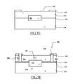
Figures 5A through 5F , a process is described for manufacturing an electronic device 500 (seeFigure 5F ) of the selective SOI type. - Considering in particular
Figure 5A , the starting material is again an SOI substrate 505 (with asemiconductor substrate 510, asemiconductor starting layer 512, and an insulating layer 115). However, in this case the insulatinglayer 515 has a thickness lower than 0.5µm, and preferably ranging from 0.2µm to 0.4µm (such as 0.3µm); likewise, thesemiconductor starting layer 512 has a thickness lower than 0.5µm, and preferably ranging from 0.1µm to 0.45µm (such as 0.3µm). - Moving now to
Figure 5B , asingle contact trench 520 is formed as above through thelayers 512, 515 (by means of two substantially anisotropic etching processes - along a vertical direction Y - through a corresponding photoresist mask 522); thecontact trench 520 likewise clears a corresponding front portion of the substrate 510 (defining abottom wall 530b) and corresponding internal portions of the startinglayer 512 and of the insulating layer 515 (definingside walls 530s). In this case, thecontact trench 520 has preferably a square shape, with each side higher than 400µm. - As shown in
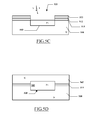
Figure 5C , two (or more) dopant implantation processes are again performed (along directions I titled as above with respect to the vertical direction Y), in order to form heavily dopedinternal regions 540 within thesubstrate 510 and the starting layer 512 (only shown for thesubstrate 510 in the figure). However, in this case theinternal region 540 is of the opposite type of conductivity with respect to thesubstrate 510 and the starting layer 512 (i.e., of the P-type). For example, Boron (B) dopant ions are used; preferably, the dopant dose ranges from 1012 ions/cm2 to 1016 ions/cm2. - The
photoresist mask 522 is likewise stripped at the end of the implantation processes. Referring now toFigure 5D , a similar epitaxial growing process is carried out so as to form anactive layer 542 of the N-type again; at the same time, the epitaxial growing process completely fills the contact trench 520 (without leaving any vacant regions). - During the epitaxial growing process, the dopant ions of the internal region 540 (shown in the
Figure 5C ) diffuse thereby forming aninsulating region 545 of the P+ type. As can be noted, theinsulating region 545 encloses the contact trench 520 (across the insulating layer 515) so as to define a PN junction with thesubstrate 510 and another PN junction with theactive layer 542. - Moving to
Figure 5E , afield oxide layer 555 is again formed on top of the active layer 542 - except for a portion thereof where a (larger)active area 557 around theinsulating region 545 is desired. - Continuing to
Figure 5F , one or more insulatingtrenches 558 are formed as described above reaching the insulating layer 515 (so as to obtain the desired electronic device 500). The insulatingtrenches 558 again partition theactive layer 542 into multipleactive regions 560, which are fully insulated by the insulatinglayer 515 and the insulatingtrenches 558. Moreover, the insulatingtrench 558 shown in the figure - around the contact trench 520 - defines a furtheractive region 561; theactive region 561 is insulated from thesubstrate 510 by means of the PN junctions formed by the insulating region 545 (when reverse-biased). - The
active regions 560 are typically used to integrate high-voltage electronic components or devices that need fast access time, low leakage and low parasitic capacitance (schematically represented in the figure as 580), so as to benefit of the typical advantages of the SOI structures. At the same time, theactive region 561 is typically used to integrate low-voltage electronic components or devices that have to dissipate heat through the semiconductor substrate (schematically represented in the figure as 581), which instead would be adversely affected by the SOI structure. As a result, it is possible to obtain a selective structure, which is well suited to house both low-voltage and high-voltage electronic components. - Naturally, in order to satisfy local and specific requirements, a person skilled in the art may apply to the solution described above many modifications and alterations. Particularly, although the present invention has been described with a certain degree of particularity with reference to preferred embodiments thereof, it should be understood that various omissions, substitutions and changes in the form and details as well as other embodiments are possible; moreover, it is expressly intended that specific elements and/or method steps described in connection with any disclosed embodiment of the invention may be incorporated in any other embodiment as a general matter of design choice.
- For example, similar considerations apply if the device has an equivalent structure (such as with layers having different thickness); moreover, although in the preceding description reference has been made to a semiconductor substrate and a starting layer of N-type, the conductivity type of these layers may be reversed (i.e., of P-type).
- It is emphasized that the described process is not to be interpreted in a limitative manner; particularly, it is possible to use equivalent steps, to remove some steps being not essential, or to add further optional steps.
- Moreover, the starting material may be either a SOI wafer already ready to be processed or a structure formed by conventional manufacturing processes.
- In any case, the implantation processes after the epitaxial growing process are not strictly necessary and they may be omitted in a simplified implementation (even if the performance of the resulting structure would be reduced).
- In any case, different beams of dopant ions can be used during the implantation processes (even with a different number of them, down to a single one).
- Moreover, nothing prevents using beams, which form a different angle with the axis of each contact trench (down to zero).
- Alternatively, it is also possible to form the contact windows at a different angle with respect to the axis of each contact trench; however, nothing prevents having some contact window along the axis of a corresponding contact trench.
- It should be noted that although in the preceding description reference has been made to a specific number of contact trenches (for the front-rear contact and the gettering region), this is not to be intended in a limitative manner; however nothing prevents forming a single contact trench even in these embodiments of the invention.
- Moreover, alternative layouts are feasible (for example, with different shapes and/or sizes of the contact trenches, or other arrangements thereof).
- Conversely, the use of more contact trenches is contemplated even in the embodiment of the invention relating to the selective SOI structure.
- Without departing from the principles of the invention, it is of course possible to form more active regions (for the front-rear-contact), more gettering regions and/or more active regions based on the PN-junction isolation - by means of corresponding insulating trenches.
- It should be readily apparent that the proposed structures may be part of the design of integrated circuits. The design may also be created in a programming language; moreover, if the designer does not fabricate chips or masks, the design may be transmitted by physical means to others. In any case, the resulting integrated circuits may be distributed by their manufacturer in raw wafer form, as bare dies, or in packages form. Moreover, the devices may be integrated with other circuits in the same chip, or they may be mounted in intermediate products (such as mother boards). In any case, the integrated circuits are suitable to be used in complex systems (such as computers).
Claims (10)
- A method for manufacturing an integrated electronic device (500), the method including the steps of:providing an SOI substrate (505) including a semiconductor substrate (510), an insulating layer (515) on the semiconductor substrate, and a semiconductor starting layer (512) on the insulating layer, the substrate and the starting layer being of a first type of conductivity,performing an epitaxial growing process, the epitaxial growing process being applied to the starting layer to obtain a thicker semiconductor active layer (542) of the first type of conductivity embedding the starting layer on the insulating layer,forming at least one insulating trench (558) extending from an exposed surface of the active layer to the insulating layer, the at least one insulating trench partitioning the active layer into insulated regions (560) and at least one further insulated region (561), andintegrating components (580) of the device in the insulated regions, the components being insulated from the substrate by the insulating layer,
characterized in that
the method further includes, before the step of performing an epitaxial growing process:forming at least one contact trench (520) extending from an exposed surface of the starting layer to the substrate in correspondence to each further insulated region, each contact trench clearing a corresponding portion (530b,530s) of the starting layer, of the insulating layer and of the substrate,implanting dopants (540) of a second type of conductivity different from the first type into at least part of the cleared portions, wherein the epitaxial growing is further applied to the cleared portions thereby at least partially filling each contact trench with semiconductor material, the dopants diffusing during the epitaxial growing to form an insulating region (545) of the second type of conductivity enclosing the at least one contact trench of each further insulated region, and integrating further components (580) of the device in each further insulated region, the further components being insulated from the substrate by a junction formed by the corresponding insulating region with the active layer and/or the substrate when reverse-biased. - The method according to claim 1, wherein the step of implanting includes:implanting at least one beam of said dopants (540) along a direction forming an angle with an axis of each contact trench (520) ranging from 2° to 45°.
- The method according to claim 2, wherein the step of implanting at least one beam of said dopants (540) includes:implanting a first beam of said dopants along a first direction forming a first angle with the axis of each contact trench (120), and implanting a second beam of said dopants along a second direction forming a second angle with the axis of each contact trench opposite the first angle.
- The method according to any claim from 1 to 3, wherein each insulating region (545) has a concentration of dopants higher than the semiconductor substrate (510) and the active layer (542).
- The method according to any claim from 1 to 4, wherein the step of forming at least one contact trench (120) includes:forming a single contact trench for each further insulated region (545).
- The method according to any claim from 1 to 5, wherein the components (580) of the device in the insulated regions (560) are high-voltage components, and the further components (581) of the device in the at least one further insulated region (561) are low-voltage components.
- An integrated electronic device (500) including:an SOI substrate (505) including a semiconductor substrate (510), an insulating layer (515) on the semiconductor substrate, a semiconductor starting layer (512) on the insulating layer, and a thicker semiconductor active layer (542) embedding the starting layer on the insulating layer, the semiconductor substrate, the starting layer and the active layer being of a first type of conductivity,at least one insulating trench (558) extending from an exposed surface of the active layer to the insulating layer, the at least one insulating trench partitioning the active layer into insulated regions (560) and at least one further insulated region (561), andcomponents (580) of the device integrated in the insulated regions, the components being insulated from the substrate by the insulating layer,
characterized byat least one contact trench (520) extending from a surface of the starting layer opposite the insulating layer to the substrate in correspondence to each further insulated region, each contact trench clearing a corresponding portion (530b,530s) of the starting layer, of the insulating layer and of the substrate,an insulating region (545) of a second type of conductivity different from the first type enclosing the at least one contact trench of each further insulated region, andfurther components (580) of the device integrated in each further insulated region, the further components being insulated from the substrate by a junction formed by the corresponding insulating region with the active layer and/or the substrate when reverse-biased. - The integrated electronic device (500) according to claim 7, wherein each insulating region (545) has a concentration of dopants higher than the semiconductor substrate (510) and the active layer (542).
- The integrated electronic device (500) according to claim 7 or 8, wherein the at least one contact trench (120) is a single contact trench for each further insulated region (545).
- The integrated electronic device (500) according to any claim from 7 to 9, wherein the components (580) of the device in the insulated regions (560) are high-voltage components, and the further components (581) of the device in each further insulated region (561) are low-voltage components.
Applications Claiming Priority (1)
| Application Number | Priority Date | Filing Date | Title |
|---|---|---|---|
| EP06116123.8A EP1873821B1 (en) | 2006-06-27 | 2006-06-27 | SOI device with contact trenches formed during epitaxial growing |
Related Parent Applications (2)
| Application Number | Title | Priority Date | Filing Date |
|---|---|---|---|
| EP06116123.8 Division | 2006-06-27 | ||
| EP06116123.8A Division-Into EP1873821B1 (en) | 2006-06-27 | 2006-06-27 | SOI device with contact trenches formed during epitaxial growing |
Publications (2)
| Publication Number | Publication Date |
|---|---|
| EP2264753A2 true EP2264753A2 (en) | 2010-12-22 |
| EP2264753A3 EP2264753A3 (en) | 2011-04-20 |
Family
ID=37432485
Family Applications (3)
| Application Number | Title | Priority Date | Filing Date |
|---|---|---|---|
| EP06116123.8A Active EP1873821B1 (en) | 2006-06-27 | 2006-06-27 | SOI device with contact trenches formed during epitaxial growing |
| EP10182985A Withdrawn EP2264752A3 (en) | 2006-06-27 | 2006-06-27 | Integrated device with both SOI insulation and junction insulation and manufacturing method |
| EP10183038A Withdrawn EP2264753A3 (en) | 2006-06-27 | 2006-06-27 | Integrated device with both SOI insulation and junction insulation and manufacturing method |
Family Applications Before (2)
| Application Number | Title | Priority Date | Filing Date |
|---|---|---|---|
| EP06116123.8A Active EP1873821B1 (en) | 2006-06-27 | 2006-06-27 | SOI device with contact trenches formed during epitaxial growing |
| EP10182985A Withdrawn EP2264752A3 (en) | 2006-06-27 | 2006-06-27 | Integrated device with both SOI insulation and junction insulation and manufacturing method |
Country Status (2)
| Country | Link |
|---|---|
| US (2) | US7635896B2 (en) |
| EP (3) | EP1873821B1 (en) |
Families Citing this family (3)
| Publication number | Priority date | Publication date | Assignee | Title |
|---|---|---|---|---|
| DE102010020884B4 (en) * | 2010-05-18 | 2018-03-15 | Infineon Technologies Ag | Semiconductor device |
| US9245788B2 (en) | 2012-04-11 | 2016-01-26 | International Business Machines Corporation | Non-bridging contact via structures in proximity |
| DE102016110588B4 (en) * | 2016-06-08 | 2020-08-13 | Infineon Technologies Ag | Semiconductor component with isolation trench and a buried lateral isolating solid-state structure and a method for its production |
Family Cites Families (22)
| Publication number | Priority date | Publication date | Assignee | Title |
|---|---|---|---|---|
| US4689656A (en) * | 1984-06-25 | 1987-08-25 | International Business Machines Corporation | Method for forming a void free isolation pattern and resulting structure |
| JPS6276645A (en) * | 1985-09-30 | 1987-04-08 | Toshiba Corp | Structure of composite semiconductor crystal |
| JP2503460B2 (en) * | 1986-12-01 | 1996-06-05 | 三菱電機株式会社 | Bipolar transistor and manufacturing method thereof |
| JPH0237771A (en) * | 1988-07-28 | 1990-02-07 | Fujitsu Ltd | Soi substrate |
| US4908328A (en) * | 1989-06-06 | 1990-03-13 | National Semiconductor Corporation | High voltage power IC process |
| US5049521A (en) * | 1989-11-30 | 1991-09-17 | Silicon General, Inc. | Method for forming dielectrically isolated semiconductor devices with contact to the wafer substrate |
| US5372952A (en) * | 1992-04-03 | 1994-12-13 | National Semiconductor Corporation | Method for forming isolated semiconductor structures |
| JP3575908B2 (en) * | 1996-03-28 | 2004-10-13 | 株式会社東芝 | Semiconductor device |
| JP2973960B2 (en) * | 1997-01-29 | 1999-11-08 | 日本電気株式会社 | Method for manufacturing semiconductor device |
| US5929508A (en) * | 1998-05-21 | 1999-07-27 | Harris Corp | Defect gettering by induced stress |
| GB9903607D0 (en) * | 1999-02-17 | 1999-04-07 | Koninkl Philips Electronics Nv | Insulated-gate field-effect semiconductor device |
| US6452234B1 (en) * | 2000-11-27 | 2002-09-17 | Advanced Micro Devices, Inc. | How to improve the ESD on SOI devices |
| US6670675B2 (en) * | 2001-08-06 | 2003-12-30 | International Business Machines Corporation | Deep trench body SOI contacts with epitaxial layer formation |
| US20050045992A1 (en) * | 2003-08-27 | 2005-03-03 | Turley Alfred P. | Bipolar/thin film SOI CMOS structure and method of making same |
| US7208815B2 (en) * | 2004-05-28 | 2007-04-24 | Taiwan Semiconductor Manufacturing Company, Ltd. | CMOS logic gate fabricated on hybrid crystal orientations and method of forming thereof |
| JP4974474B2 (en) * | 2004-06-22 | 2012-07-11 | ルネサスエレクトロニクス株式会社 | Semiconductor device and manufacturing method thereof |
| EP1630863B1 (en) * | 2004-08-31 | 2014-05-14 | Infineon Technologies AG | Method of fabricating a monolithically integrated vertical semiconducting device in an soi substrate |
| US6972478B1 (en) * | 2005-03-07 | 2005-12-06 | Advanced Micro Devices, Inc. | Integrated circuit and method for its manufacture |
| US7811915B2 (en) * | 2006-05-01 | 2010-10-12 | Spansion Llc | Method for forming bit lines for semiconductor devices |
| US7544548B2 (en) * | 2006-05-31 | 2009-06-09 | Freescale Semiconductor, Inc. | Trench liner for DSO integration |
| US7595232B2 (en) * | 2006-09-07 | 2009-09-29 | International Business Machines Corporation | CMOS devices incorporating hybrid orientation technology (HOT) with embedded connectors |
| US7820501B2 (en) * | 2006-10-11 | 2010-10-26 | International Business Machines Corporation | Decoder for a stationary switch machine |
-
2006
- 2006-06-27 EP EP06116123.8A patent/EP1873821B1/en active Active
- 2006-06-27 EP EP10182985A patent/EP2264752A3/en not_active Withdrawn
- 2006-06-27 EP EP10183038A patent/EP2264753A3/en not_active Withdrawn
-
2007
- 2007-06-19 US US11/820,393 patent/US7635896B2/en active Active
-
2009
- 2009-11-02 US US12/610,463 patent/US8183098B2/en active Active
Non-Patent Citations (1)
| Title |
|---|
| None |
Also Published As
| Publication number | Publication date |
|---|---|
| US7635896B2 (en) | 2009-12-22 |
| EP2264752A3 (en) | 2011-04-20 |
| EP1873821A1 (en) | 2008-01-02 |
| EP2264753A3 (en) | 2011-04-20 |
| EP1873821B1 (en) | 2015-11-11 |
| US20070296036A1 (en) | 2007-12-27 |
| EP2264752A2 (en) | 2010-12-22 |
| US8183098B2 (en) | 2012-05-22 |
| US20100075484A1 (en) | 2010-03-25 |
Similar Documents
| Publication | Publication Date | Title |
|---|---|---|
| US20210320119A1 (en) | Three-dimensional memory device and method for forming the same | |
| US9214390B2 (en) | Method for forming through-silicon via (TSV) with diffused isolation well | |
| US10672901B2 (en) | Power transistor with terminal trenches in terminal resurf regions | |
| US20130087852A1 (en) | Edge termination structure for power semiconductor devices | |
| US20120261804A1 (en) | Vertical substrate diode, method of manufacture and design structure | |
| CN111009574B (en) | Bipolar transistor | |
| US20130307064A1 (en) | Power transistor device and fabricating method thereof | |
| US20210005599A1 (en) | Internally stacked npn with segmented collector | |
| KR101793214B1 (en) | Thyristor random access memory device and method | |
| US11145741B2 (en) | Bipolar transistor | |
| US8183098B2 (en) | SOI device with contact trenches formed during epitaxial growing | |
| US20230411386A1 (en) | Method and structure of forming contacts and gates for staggered fet | |
| TW202349634A (en) | Via to backside power rail through active region | |
| US20050145981A1 (en) | Methods for manufacturing SOI substrate using wafer bonding and complementary high voltage bipolar transistor using the SOI substrate | |
| KR20080073313A (en) | Semiconductor device and manufacturing method thereof | |
| US8816429B2 (en) | Charge balance semiconductor devices with increased mobility structures | |
| US7714382B2 (en) | Trench gate semiconductor with NPN junctions beneath shallow trench isolation structures | |
| US20260096188A1 (en) | Semiconductor device and manufacturing method thereof | |
| TWI883976B (en) | Semiconductor structure and manufacturing method thereof | |
| US12635488B2 (en) | Merged trenches surrounded by wider trench for isolating semiconductor devices | |
| US20240145293A1 (en) | Merged trenches surrounded by wider trench for isolating semiconductor devices | |
| EP4365953A2 (en) | Transistors having backside contact structures | |
| US20250366084A1 (en) | Diode trench isolation for improved breakdown voltage uniformity | |
| US7999349B2 (en) | Front-rear contacts of electronics devices with induced defects to increase conductivity thereof | |
| TW202614210A (en) | Semiconductor device and manufacturing method thereof |
Legal Events
| Date | Code | Title | Description |
|---|---|---|---|
| PUAI | Public reference made under article 153(3) epc to a published international application that has entered the european phase |
Free format text: ORIGINAL CODE: 0009012 |
|
| AC | Divisional application: reference to earlier application |
Ref document number: 1873821 Country of ref document: EP Kind code of ref document: P |
|
| AK | Designated contracting states |
Kind code of ref document: A2 Designated state(s): DE FR GB IT |
|
| PUAL | Search report despatched |
Free format text: ORIGINAL CODE: 0009013 |
|
| AK | Designated contracting states |
Kind code of ref document: A3 Designated state(s): DE FR GB IT |
|
| RIC1 | Information provided on ipc code assigned before grant |
Ipc: H01L 21/762 20060101ALI20110316BHEP Ipc: H01L 21/84 20060101ALI20110316BHEP Ipc: H01L 21/76 20060101AFI20110316BHEP Ipc: H01L 27/12 20060101ALI20110316BHEP |
|
| STAA | Information on the status of an ep patent application or granted ep patent |
Free format text: STATUS: THE APPLICATION IS DEEMED TO BE WITHDRAWN |
|
| 18D | Application deemed to be withdrawn |
Effective date: 20111021 |