EP2261795A1 - Circuits and methods for performing exponentiation and inversion of finite field elements - Google Patents
Circuits and methods for performing exponentiation and inversion of finite field elements Download PDFInfo
- Publication number
- EP2261795A1 EP2261795A1 EP10161704A EP10161704A EP2261795A1 EP 2261795 A1 EP2261795 A1 EP 2261795A1 EP 10161704 A EP10161704 A EP 10161704A EP 10161704 A EP10161704 A EP 10161704A EP 2261795 A1 EP2261795 A1 EP 2261795A1
- Authority
- EP
- European Patent Office
- Prior art keywords
- field element
- exponentiation
- output
- digits
- circuits
- Prior art date
- Legal status (The legal status is an assumption and is not a legal conclusion. Google has not performed a legal analysis and makes no representation as to the accuracy of the status listed.)
- Granted
Links
Images


Classifications
-
- G—PHYSICS
- G06—COMPUTING OR CALCULATING; COUNTING
- G06F—ELECTRIC DIGITAL DATA PROCESSING
- G06F7/00—Methods or arrangements for processing data by operating upon the order or content of the data handled
- G06F7/60—Methods or arrangements for performing computations using a digital non-denominational number representation, i.e. number representation without radix; Computing devices using combinations of denominational and non-denominational quantity representations, e.g. using difunction pulse trains, STEELE computers, phase computers
- G06F7/72—Methods or arrangements for performing computations using a digital non-denominational number representation, i.e. number representation without radix; Computing devices using combinations of denominational and non-denominational quantity representations, e.g. using difunction pulse trains, STEELE computers, phase computers using residue arithmetic
- G06F7/724—Finite field arithmetic
- G06F7/726—Inversion; Reciprocal calculation; Division of elements of a finite field
Definitions
- Finite field arithmetic is highly useful in such forward error correction algorithms. Encryption algorithms also commonly use finite field arithmetic.
- a finite field commonly called a Galois field
- a Galois field is a field that contains only a finite number of numerical elements.
- One example of a Galois field is a set of five-digit binary numbers. There are a total of 32 such numbers and, for example, 31 of those numbers could constitute a Galois field.
- An important characteristic of a Galois field is that the arithmetic operators (addition, subtraction, multiplication, and division) are defined such that any arithmetic operation performed on elements of the field will always yield one of the elements in the field.
- the addition and subtraction operations can be carried out as exclusive-OR (XOR) logic operations
- multiplication can be carried out as logical shifts, AND, and XOR operations.
- the multiplicative inverse of an element of a Galois field can be found either by using a ROM-based a look-up table (LUT) or by using a recursive circuit to implement Fermat's Little Theorem (Pierre de Fermat, first published in 1640).
- LUT look-up table
- equation (2) the ability to efficiently raise a Galois field element to a power of 2 m , i.e., 2, 4, 8, etc., is of critical importance.
- equation (3) it is the ability to efficiently square a Galois field element that is the most critical item.
- the ⁇ m operation is performed via a recursive application of a squaring operation, which is accomplished by multiplying the field element by itself.
- Fig. 1 illustrates a serial computation architecture 100 required to implement the approach of equation (2).
- a squaring operation 102 denoted by ( ) 2 is performed on the element ⁇ to produce ⁇ 2 .
- a second squaring operation 104 is performed on the output ⁇ 2 of the first squaring operation 102 to produce ⁇ 4 .
- a first multiplication operation 106 is then performed on the outputs of the first and second squaring operations 102 and 104 ( ⁇ 2 and ⁇ 4 ) to yield ⁇ 6 .
- a third squaring operation 108 is performed on the output ⁇ 4 of the second squaring operation 104 to produce ⁇ 8 .
- a second multiplication operation 110 is then performed on the outputs of the first multiplication operation 106 ( ⁇ 6 ) and the third squaring operation 108 ( ⁇ 8 ) to yield ⁇ 14 .
- This process is repeated for m-2 stages until the output of the multiplier of the m -2 th stage yields ⁇ N-2 .
- Each of the squaring operations and multiplication operations can be carried out by performing an actual multiplication operation in hardware or software or by using a look-up table.
- Fig. 2 illustrates the serial computation architecture 200 required to implement the approach of equation (3).
- a squaring operation 202 denoted by ( ) 2 is performed on the element ⁇ to produce ⁇ 2 .
- a second squaring operation 204 is performed on the output ⁇ 2 of the first squaring operation 202 to produce ⁇ 4 .
- a first multiplication operation 206 is then performed on the outputs of the first and second squaring operations 202 and 204 ( ⁇ 2 and ⁇ 4 ) to yield ⁇ 6 .
- a third squaring operation 208 is performed on the output ⁇ 6 of the first multiplication operation 206 to produce ⁇ 12 .
- a second multiplication operation 210 is then performed on the output of the third squaring operation 208 ( ⁇ 12 ) and the output of the first squaring operation 202 ( ⁇ 2 ) to yield ⁇ 14 .
- This process is repeated for m-2 stages until the output of the m -2 th stage yields ⁇ N-2 .
- a technique is described herein for constructing a field exponentiation circuit to any power of 2 m based upon matrix algebra, which greatly reduces the amount of hardware required, reduces the processing delay through the circuit, and increases data throughput.
- the field exponentiation circuit is particularly useful for computing powers of an element of a Galois field having an exponent of 2 m (i.e., powers of 2, 4, 8, 16, etc.), which can be used to compute the multiplicative inverse of the element as necessary to carry out division.
- an exponentiation circuit for computing an exponential power of a finite field element includes combinatory logic circuits that map input digits (e.g., bits) of a multi-digit field element ⁇ to output digits (bits) of an output multi-digit field element ⁇ 2 m .
- Certain output digits are generated by the combinatory logic circuits as logical combinations of certain input digits.
- at least some of the output digits are generated by the combinatory logic circuits from only one of the input digits by directly mapping an input digit to an output digit.
- An underlying exponentiation matrix determines the mapping of the input bits to the output bits and can be implemented in combinatory logic circuits requiring only exclusive-OR combinations. In this manner, the exponentiation circuit is capable of computing a power of a field element without performing any multiplication operations.
- a circuit for generating a multiplicative inverse of a finite field element can be constructed from a plurality of parallel exponentiation circuits, with each of the parallel exponentiation circuits generating a different multi-digit field element ⁇ 2 m directly from the input field element ⁇ .
- Multiplier circuits multiply together the outputs of the parallel exponentiation circuits to generate the multiplicative inverse of the field element ⁇ .
- the underlying matrix algebra concept can be further extended to construct circuits that multiply a finite field element by a constant using only combinatory logic circuits.
- the invention refers to an exponentiation circuit for computing an exponential power of a finite field element, comprising: combinatory logic circuits configured to receive input digits of a multi-digit field element ⁇ of a finite field, the combinatory logic circuits mapping the input digits to output digits of an output multi-digit field element ⁇ 2 m , where m is an integer greater than zero.
- At least some of the output digits can be generated by the combinatory logic circuits as logical combinations of certain input digits and at least some of the output digits are generated by the combinatory logic circuits from only one of the input digits by directly mapping an input digit to an output digit. Further in one embodiment the exponentiation circuit does not perform any multiplication operations. Logical combinations generated by the combinatory logic circuits can include only exclusive-OR combinations. The combinatory logic circuits can implement logical relationships between the field element ⁇ and the output field element ⁇ 2 m specified by an exponentiation matrix.
- the exponentiation matrix implemented by the combinatory logic circuits can be an n x n matrix equal to the transform of the first n elements of the finite field raised to the 2 m power, where n is the number of digits of the multi-digit field element ⁇ .
- the invention also relates to a circuit for generating a multiplicative inverse of a finite field element, comprising a plurality of parallel exponentiation circuits, each of the parallel exponentiation circuits receiving a multi-digit field element ⁇ and generating an output multi-digit field element ⁇ 2 m , where m is an integer greater than zero; a plurality of multiplier circuits configured to multiply together outputs of the parallel exponentiation circuits to generate the multiplicative inverse of the field element ⁇ .
- the parallel exponentiation circuits may not perform any multiplication operations.
- the parallel exponentiation circuits can generate exponential powers of the field element ⁇ using only combinatory logic on the digits of the field element ⁇ .
- the combinatory logic can include only exclusive-OR combinations.
- the combinatory logic can implement logical relationships between the field element ⁇ and the output field element ⁇ 2 m specified by an exponentiation matrix.
- the multi-digit field element ⁇ can be a multi-bit binary field element.
- Each of the exponentiation circuits can be implemented with a look-up table; a plurality of exclusive-OR gates; and/or software.
- the invention also relates to a circuit for multiplying a finite field element by a constant, comprising: combinatory logic circuits configured to receive input digits of a multi-digit field element ⁇ of a finite field, the combinatory logic circuits mapping the input digits to output digits of an output multi-digit field element ⁇ n x ⁇ , where ⁇ n is a constant and n is an integer greater than zero.
- the invention also relates to a method for generating an exponential power of a finite field element, comprising: receiving input digits of a multi-digit field element ⁇ of a finite field at an exponentiation circuit; mapping via combinatory logic circuits the input digits to output digits of an output multi-digit field element ⁇ 2 m , where m is an integer greater than zero; and supplying the output multi-digit field element ⁇ 2 m as an output of the exponentiation circuit.
- At least some of the output digits can be generated by the combinatory logic circuits as logical combinations of certain input digits and at least some of the output digits are generated by the combinatory logic circuits from only one of the input digits by directly mapping an input digit to an output digit.
- the method can be carried out without performing any multiplication operations.
- Logical combinations can include only exclusive-OR combinations.
- the method can implement, via the combinatory logic circuits, logical relationships between the field element ⁇ and the output field element ⁇ 2 m specified by an exponentiation matrix.
- the method can further comprise receiving the multi-digit field element ⁇ at a plurality of parallel exponentiation circuits, each of the parallel exponentiation circuits generating an output multi-digit field element ⁇ 2 m for a different value of m; and multiplying together outputs of the parallel exponentiation circuits to generate the multiplicative inverse of the field element ⁇ .
- Fig. 1 is a block diagram illustrating a serial computation architecture for computing a multiplicative inverse of an element of a Galois field.
- Fig. 2 is a block diagram illustrating another serial computation architecture for computing a multiplicative inverse of an element of a Galois field.
- Fig. 3 is a block diagram illustrating a parallel computation architecture for computing a multiplicative inverse of an element of a Galois field in accordance with an embodiment of the invention.
- Figs. 4A-D are circuit diagrams illustrating logic circuits for generating powers of an element of a Galois field required to compute the multiplicative inverse of the element for a specific generator polynomial.
- Fig. 5 is a flow diagram illustrating operations to perform exponentiation of an element of a Galois field and to generate a multiplicative inverse of an element of a Galois field in accordance with an embodiment of the invention.
- Fig. 6 is a circuit diagram illustrating logic circuits for multiplying an element of a Galois field by a constant according to another embodiment of the invention.
- the invention described herein presents a novel technique for constructing a field exponentiation circuit to any power of 2 m based upon matrix algebra, which greatly reduces the amount of hardware required, reduces the processing delay through the circuit, and increases the data throughput.
- the field exponentiation circuit is particularly useful for computing powers of an element of a Galois field having an exponent of 2 m (i.e., powers of 2, 4, 8, 16, etc.), which can be used to compute the multiplicative inverse of the element as necessary to carry out division in accordance with equation (1).
- Fig. 3 is a block diagram illustrating the circuit topology for the approach described herein.
- the architecture depicted in Fig. 3 is a conceptual diagram illustrating major functional units, and does not necessarily illustrate physical relationships.
- powers of 2 m of an input element ⁇ are computed to support determination of the multiplicative inverse ⁇ -1 according to equation (2) above.
- the circuit topology shown in Fig. 3 has the advantage of computing the several ⁇ 2 m component values in parallel and computing products of these values in parallel, which decreases the data throughput delay.
- the input element ⁇ whose inverse is to be determined is supplied directly to each exponentiation circuit 302, 304, 306, and 308 in parallel.
- Exponentiation circuit 302 generates an output ⁇ 2 .
- exponentiation circuit 304 generates an output ⁇ 4
- exponentiation circuit 306 generates an output ⁇ 8
- exponentiation circuit 308 generates an output ⁇ 16 , and so on up to ⁇ 2m-1 . Note that all of these circuits generate their respective power of ⁇ directly from the input of the element ⁇ itself. None of the outputs of any of the exponentiation circuits is used as an input to any other exponentiation circuits.
- a multiplication circuit 310 performs a multiplication operation on the output of exponentiation circuit 302 ( ⁇ 2 ) and the output of exponentiation circuit 304 ( ⁇ 4 ) to yield ⁇ 6 .
- a multiplication circuit 312 performs a multiplication operation on the output of exponentiation circuit 306 ( ⁇ 8 ) and the output of exponentiation circuit 308 ( ⁇ 16 ) to yield ⁇ 24 .
- the multiplication circuits 310, 312, and 314 shown in Fig. 3 can be implemented in hardware and/or software and can carry out a multiplication operation or be implemented as a look-up table.
- the technique described herein is capable of generating the ⁇ 2 m elements in a manner that both requires less circuitry and that is considerably faster than traditional circuitry.
- Each of the parallel exponential stages requires only simple logic circuitry to generate the output exponential value from the input element value and completely avoids the need to perform multiplication operations in the exponential stages or the need for a serial arrangement of any exponential stages.
- any of the exponential operations, multiplication operations, and logical components thereof shown in the figures can be implemented in hardware, software, look-up tables, or combinations thereof, and the terms “circuit” and “circuitry” are to be understood to cover any of these implementations.
- ⁇ is an element of a Galois field of size 2 n ( ⁇ ⁇ GF (2 n )
- ⁇ 2 is computed as follows:
- ⁇ 2 m is an exponentiation matrix and is equal to the transform of the first n elements of the field raised to the 2 m power. This matrix is multiplied by the vector form of the field value, using standard sum of product computations, to generate the result. Note that the transform matrix will contain only values of 0 and 1, thereby greatly simplifying the array computations. Also note that the transform matrix is a constant given a specific generator polynomial, and thus can be pre-computed. The result is a simple transformation of the input field value.
- a generator polynomial is an equation used to adapt the arithmetic operations in a Galois field in a modulo manner such that any arithmetic operation on elements of the field result in another element of the field.
- ⁇ in the foregoing example are coefficients of a polynomial: ⁇ 4 ⁇ ⁇ 4 + ⁇ 3 ⁇ ⁇ 3 + ⁇ 2 ⁇ ⁇ 2 + ⁇ 1 ⁇ ⁇ 1 + ⁇ 0 ⁇ ⁇ 0
- equation (2) Given a method for constructing a circuit to compute ⁇ 2 m , an efficient multiplicative inversion technique can be constructed, using the equality from equation (2). Note that all the terms of equation (2) are of the form ⁇ 2 m and are functions of the input field value ⁇ . Therefore, all the terms can be computed in parallel and the product can be computed using a balanced multiplication tree, as shown previously in Fig. 3 .
- the circuit also uses the pre-computed exponentiation matrix that is both smaller and faster than traditional circuitry.
- ⁇ 0 is expressed as the row of values 00001
- ⁇ 1 is expressed as the row of values 00010
- ⁇ 2 is expressed as the row of values 00100
- ⁇ 3 is expressed as the row of values 01000
- ⁇ 4 is expressed as the row of values 10000.
- This array maps into the digital logic circuit shown in Fig. 4A .
- the exponentiation circuit 302 shown in Fig. 3 can be implemented with the logic circuit shown in Fig. 4A .
- ⁇ 4 ⁇ 4 ⁇ ⁇ 1
- ⁇ 3 4 ⁇ 4 ⁇ ⁇ 3 ⁇ ⁇ 2
- ⁇ 2 4 ⁇ 3 ⁇ ⁇ 2
- ⁇ 1 4 ⁇ 4 ⁇ ⁇ 3
- ⁇ 0 4 ⁇ 4 ⁇ ⁇ 2 ⁇ ⁇ 0 .
- the ⁇ 8 exponential generator 306 shown in Fig. 4C maps the input bits of an element ⁇ into the output bits of ⁇ 8 .
- ⁇ 8 ⁇ 8 x ⁇ .
- the ⁇ 16 exponential generator 308 shown in Fig. 4D maps the input bits of an element ⁇ into the output bits of ⁇ 16 .
- ⁇ 16 ⁇ 16 x ⁇ .
- Table 1 Galois field Exponentiation Function Requirements Value Exclusive-OR Functions FPGA LUTs ⁇ 2 3 3 ⁇ 4 7 5 ⁇ 8 8 5 ⁇ 16 5 3 Total 23 16
- a full Galois multiplier requires 19 2-input Exclusive-OR functions and 16 2-input logical AND functions.
- all the exponentiation operations required to perform a multiplicative inversion occur in approximately one-third the size of a single Galois field multiplier.
- Figs. 1 and 2 The multi-stage serial squaring-and-multiplying techniques illustrated in Figs. 1 and 2 are convenient from the standpoint that a standard multiplier circuit can be used to carry out both the squaring and multiplication operations (the squaring operation involves multiplying an input by itself), and the multiplicative inverse of a finite field element can be computed by stringing together a number of such multiplier circuits in a multi-stage configuration.
- a unique aspect of the technique described herein is that the 2 m powers of a finite field element are computed in a more elegant and efficient manner without the use of multipliers or look-up tables that implement multiplication operations. Rather, the technique is based on the insight that there is actually a combinatorial way to represent the 2 m powers of a finite field element which is much simpler and can be implemented in parallel.
- equation (8) is important in understanding how exponentiation circuits can be constructed with relatively few components and/or operations.
- the cross-products keep disappearing (canceling out) such that the computations do not become more complex even at higher powers of ⁇ .
- This characteristic permits the relationships between ⁇ and the powers of ⁇ to be represented in a simple n x n exponentiation matrix which transforms the digits (in this case bits) of ⁇ to digits (bits) of the output power of ⁇ ( ⁇ 2 m ).
- the exponentiation matrix can be implemented using only combinatory logic, where each bit of the output exponential ⁇ 2 m is either equal to the value of one of the input bits of ⁇ or an exclusive-OR combination of certain bits of ⁇ . This is because, by its nature, the exponentiation matrix yields summations of input bits, which are performed logically as an exclusive-OR operation.
- combinatory logic and combinatory logic circuits refer to circuitry (implemented in hardware, software, look-up tables, or combinations thereof) that maps input digits to output digits based on only logical relationships. These logical relationships include mapping logical combinations of certain input digits of an input field element to output digits of the output field element.
- logical relationships may also include the direct mapping of an input digit to an output digit in some instances, as shown for example with the direct mapping of input bit ⁇ 2 to output bit ⁇ 4 2 in exponentiation circuit 302 in Fig. 4A .
- All of the logical combinations employed by the combinatory logic are exclusive-OR combinations of the input digits.
- Fig. 5 is a flow diagram summarizing the operations performed to carry out exponentiation of a finite field element and computation of the multiplicative inverse of a field element in accordance with an embodiment of the invention.
- a multi-digit field element ⁇ of a finite field is supplied to each of a plurality of parallel exponentiation circuits.
- each of the exponentiation circuits essentially maps the digits of the input field element ⁇ to output digits of an output multi-digit field element ⁇ 2 m , which is a 2 m power of the input field element ⁇ , where m is an integer greater than zero and where the value of m is different for each exponentiation circuit. This mapping is accomplished using combinatory logic circuits.
- the output multi-digit field elements ⁇ 2 m from each of the parallel exponentiation circuits are multiplied together to generate the multiplicative inverse of the field element ⁇ .
- ⁇ N ⁇ ⁇ ⁇ N ⁇ ⁇
- the invention encompasses the use of matrix algebra with finite field elements, resulting in arrays that are summations of input values that can be used to raise a field element to a power or to carry out multiplication by a constant.
- the invention can be used in any hardware or software application that requires finite field arithmetic, such as encryption or forward error correction algorithms.
- finite field arithmetic such as encryption or forward error correction algorithms.
- forward error correction codes are used extensively in communications to ensure the accuracy of data being received.
- Properly encoding data with finite field arithmetic allows a relatively small check word to be used to check the accuracy of a large amount of data and to determine which data is erroneous.
- the computations required to perform these types of operations can be carried out with less hardware and/or less and faster processing.
Landscapes
- Physics & Mathematics (AREA)
- Engineering & Computer Science (AREA)
- General Physics & Mathematics (AREA)
- Mathematical Analysis (AREA)
- Mathematical Optimization (AREA)
- Pure & Applied Mathematics (AREA)
- Computational Mathematics (AREA)
- Theoretical Computer Science (AREA)
- Computing Systems (AREA)
- Mathematical Physics (AREA)
- General Engineering & Computer Science (AREA)
- Error Detection And Correction (AREA)
- Detection And Correction Of Errors (AREA)
Abstract
Description
- Communication systems, particularly wireless communications and highspeed transmissions, often require the use of forward error correction algorithms to identify bit errors in received signals. Finite field arithmetic is highly useful in such forward error correction algorithms. Encryption algorithms also commonly use finite field arithmetic.
- A finite field, commonly called a Galois field, is a field that contains only a finite number of numerical elements. One example of a Galois field is a set of five-digit binary numbers. There are a total of 32 such numbers and, for example, 31 of those numbers could constitute a Galois field. An important characteristic of a Galois field is that the arithmetic operators (addition, subtraction, multiplication, and division) are defined such that any arithmetic operation performed on elements of the field will always yield one of the elements in the field. In the binary example given, the addition and subtraction operations can be carried out as exclusive-OR (XOR) logic operations, and multiplication can be carried out as logical shifts, AND, and XOR operations. Note that in some cases, such operations will yield results that are not within the set of five-digit numbers. However, as applied within the Galois field, these arithmetic operations are defined using an irreducible generator polynomial which creates a modulo operation on the result, whereby the result remains within the Galois field (i.e., the result is one of the finite number of elements).
- In the discipline of Galois field mathematics, addition, subtraction, and multiplication of field elements are well understood, and these operations can be mapped efficiently into hardware or software domains. However, dividing one field element by another in a Galois field does not map very efficiently into either of the hardware or software domains. The most accepted way of performing division is to multiply the dividend by the multiplicative inverse of the divisor, as follows:

- Fermat's Little Theorem states that, for any Galois field element β, the multiplicative inverse can be found by computing β-1 = β N-2, where N is the total number of elements in the field. β N-2 can be found recursively via two methods:


where 2 m = N+1. Using equation (2), the ability to efficiently raise a Galois field element to a power of 2 m , i.e., 2, 4, 8, etc., is of critical importance. In equation (3), it is the ability to efficiently square a Galois field element that is the most critical item. For either recursive approach, the β m operation is performed via a recursive application of a squaring operation, which is accomplished by multiplying the field element by itself. -
Fig. 1 illustrates aserial computation architecture 100 required to implement the approach of equation (2). In particular, asquaring operation 102 denoted by ( )2 is performed on the element β to produce β2. Asecond squaring operation 104 is performed on the output β2 of thefirst squaring operation 102 to produce β4. Afirst multiplication operation 106 is then performed on the outputs of the first andsecond squaring operations 102 and 104 (β2 and β4) to yield β6. Athird squaring operation 108 is performed on the output β4 of thesecond squaring operation 104 to produce β8. Asecond multiplication operation 110 is then performed on the outputs of the first multiplication operation 106 (β6) and the third squaring operation 108 (β8) to yield β14. This process is repeated for m-2 stages until the output of the multiplier of the m-2th stage yields βN-2. For example, where m = 5 and 2 m = N+1 = 32, the circuit inFig. 1 would include one additional stage withsquaring operation 112 andmultiplication operation 114 to yield an output value β30 = β -1. Each of the squaring operations and multiplication operations can be carried out by performing an actual multiplication operation in hardware or software or by using a look-up table. -
Fig. 2 illustrates theserial computation architecture 200 required to implement the approach of equation (3). In particular, asquaring operation 202 denoted by ( )2 is performed on the element β to produce β2. Asecond squaring operation 204 is performed on the output β2 of thefirst squaring operation 202 to produce β4. Afirst multiplication operation 206 is then performed on the outputs of the first andsecond squaring operations 202 and 204 (β2 and β4) to yield β6. Athird squaring operation 208 is performed on the output β6 of thefirst multiplication operation 206 to produce β12. Asecond multiplication operation 210 is then performed on the output of the third squaring operation 208 (β12) and the output of the first squaring operation 202 (β2) to yield β14. This process is repeated for m-2 stages until the output of the m-2th stage yields βN-2. For example, where m = 5 and 2 m = N+1 = 32, the circuit inFig. 2 would include one additional stage withsquaring operation 212 andmultiplication operation 214 to yield an output value β30 = β-1. - The types of serial architecture shown in
Figs. 1 and 2 have long computation delays, decreasing the data throughput. Accordingly, there remains a need for an efficient approach to computing the multiplicative inverse of elements in a Galois field. - A technique is described herein for constructing a field exponentiation circuit to any power of 2 m based upon matrix algebra, which greatly reduces the amount of hardware required, reduces the processing delay through the circuit, and increases data throughput. The field exponentiation circuit is particularly useful for computing powers of an element of a Galois field having an exponent of 2 m (i.e., powers of 2, 4, 8, 16, etc.), which can be used to compute the multiplicative inverse of the element as necessary to carry out division.
- In accordance with one embodiment, an exponentiation circuit for computing an exponential power of a finite field element includes combinatory logic circuits that map input digits (e.g., bits) of a multi-digit field element β to output digits (bits) of an output multi-digit field element β2m . Certain output digits are generated by the combinatory logic circuits as logical combinations of certain input digits. In some instances, at least some of the output digits are generated by the combinatory logic circuits from only one of the input digits by directly mapping an input digit to an output digit.
- An underlying exponentiation matrix determines the mapping of the input bits to the output bits and can be implemented in combinatory logic circuits requiring only exclusive-OR combinations. In this manner, the exponentiation circuit is capable of computing a power of a field element without performing any multiplication operations.
- A circuit for generating a multiplicative inverse of a finite field element can be constructed from a plurality of parallel exponentiation circuits, with each of the parallel exponentiation circuits generating a different multi-digit field element β2m directly from the input field element β. Multiplier circuits multiply together the outputs of the parallel exponentiation circuits to generate the multiplicative inverse of the field element β. The underlying matrix algebra concept can be further extended to construct circuits that multiply a finite field element by a constant using only combinatory logic circuits.
- The invention refers to an exponentiation circuit for computing an exponential power of a finite field element, comprising: combinatory logic circuits configured to receive input digits of a multi-digit field element β of a finite field, the combinatory logic circuits mapping the input digits to output digits of an output multi-digit field element β2m , where m is an integer greater than zero.
- Further embodiments are mentioned below. These embodiments an be combined in any way. At least some of the output digits can be generated by the combinatory logic circuits as logical combinations of certain input digits and at least some of the output digits are generated by the combinatory logic circuits from only one of the input digits by directly mapping an input digit to an output digit. Further in one embodiment the exponentiation circuit does not perform any multiplication operations. Logical combinations generated by the combinatory logic circuits can include only exclusive-OR combinations. The combinatory logic circuits can implement logical relationships between the field element β and the output field element β2m specified by an exponentiation matrix. The exponentiation matrix implemented by the combinatory logic circuits can be an n x n matrix equal to the transform of the first n elements of the finite field raised to the 2 m power, where n is the number of digits of the multi-digit field element β.
- The invention also relates to a circuit for generating a multiplicative inverse of a finite field element, comprising a plurality of parallel exponentiation circuits, each of the parallel exponentiation circuits receiving a multi-digit field element β and generating an output multi-digit field element β2m , where m is an integer greater than zero; a plurality of multiplier circuits configured to multiply together outputs of the parallel exponentiation circuits to generate the multiplicative inverse of the field element β.
- In the following preferred embodiments are mentioned which can be combined in any way. The parallel exponentiation circuits may not perform any multiplication operations. The parallel exponentiation circuits can generate exponential powers of the field element β using only combinatory logic on the digits of the field element β. The combinatory logic can include only exclusive-OR combinations. The combinatory logic can implement logical relationships between the field element β and the output field element β2m specified by an exponentiation matrix. The multi-digit field element β can be a multi-bit binary field element. Each of the exponentiation circuits can be implemented with a look-up table; a plurality of exclusive-OR gates; and/or software.
- The invention also relates to a circuit for multiplying a finite field element by a constant, comprising: combinatory logic circuits configured to receive input digits of a multi-digit field element β of a finite field, the combinatory logic circuits mapping the input digits to output digits of an output multi-digit field element α n x β, where α n is a constant and n is an integer greater than zero.
- The invention also relates to a method for generating an exponential power of a finite field element, comprising: receiving input digits of a multi-digit field element β of a finite field at an exponentiation circuit; mapping via combinatory logic circuits the input digits to output digits of an output multi-digit field element β2m , where m is an integer greater than zero; and supplying the output multi-digit field element β2m as an output of the exponentiation circuit.
- In the following preferred embodiments are mentioned which can be combined in any way. At least some of the output digits can be generated by the combinatory logic circuits as logical combinations of certain input digits and at least some of the output digits are generated by the combinatory logic circuits from only one of the input digits by directly mapping an input digit to an output digit. The method can be carried out without performing any multiplication operations. Logical combinations can include only exclusive-OR combinations. The method can implement, via the combinatory logic circuits, logical relationships between the field element β and the output field element β2m specified by an exponentiation matrix. The method can further comprise receiving the multi-digit field element β at a plurality of parallel exponentiation circuits, each of the parallel exponentiation circuits generating an output multi-digit field element β2m for a different value of m; and multiplying together outputs of the parallel exponentiation circuits to generate the multiplicative inverse of the field element β.
- The above and still further features and advantages of the present invention will become apparent upon consideration of the following definitions, descriptions and descriptive figures of specific embodiments thereof wherein like reference numerals in the various figures are utilized to designate like components. While these descriptions go into specific details of the invention, it should be understood that variations may and do exist and would be apparent to those skilled in the art based on the descriptions herein.
-
Fig. 1 is a block diagram illustrating a serial computation architecture for computing a multiplicative inverse of an element of a Galois field. -
Fig. 2 is a block diagram illustrating another serial computation architecture for computing a multiplicative inverse of an element of a Galois field. -
Fig. 3 is a block diagram illustrating a parallel computation architecture for computing a multiplicative inverse of an element of a Galois field in accordance with an embodiment of the invention. -
Figs. 4A-D are circuit diagrams illustrating logic circuits for generating powers of an element of a Galois field required to compute the multiplicative inverse of the element for a specific generator polynomial. -
Fig. 5 is a flow diagram illustrating operations to perform exponentiation of an element of a Galois field and to generate a multiplicative inverse of an element of a Galois field in accordance with an embodiment of the invention. -
Fig. 6 is a circuit diagram illustrating logic circuits for multiplying an element of a Galois field by a constant according to another embodiment of the invention. - The invention described herein presents a novel technique for constructing a field exponentiation circuit to any power of 2 m based upon matrix algebra, which greatly reduces the amount of hardware required, reduces the processing delay through the circuit, and increases the data throughput. The field exponentiation circuit is particularly useful for computing powers of an element of a Galois field having an exponent of 2 m (i.e., powers of 2, 4, 8, 16, etc.), which can be used to compute the multiplicative inverse of the element as necessary to carry out division in accordance with equation (1).
-
Fig. 3 is a block diagram illustrating the circuit topology for the approach described herein. The architecture depicted inFig. 3 is a conceptual diagram illustrating major functional units, and does not necessarily illustrate physical relationships. Like the circuit topology shown inFig. 1 , powers of 2 m of an input element β are computed to support determination of the multiplicative inverse β-1 according to equation (2) above. However, the circuit topology shown inFig. 3 has the advantage of computing the several β2m component values in parallel and computing products of these values in parallel, which decreases the data throughput delay. In particular, the input element β whose inverse is to be determined is supplied directly to eachexponentiation circuit Exponentiation circuit 302 generates an output β2. In parallel withcircuit 302,exponentiation circuit 304 generates an output β4,exponentiation circuit 306 generates an output β8,exponentiation circuit 308 generates an output β16, and so on up to β2m-1. Note that all of these circuits generate their respective power of β directly from the input of the element β itself. None of the outputs of any of the exponentiation circuits is used as an input to any other exponentiation circuits. - As shown in
Fig. 3 , the outputs of exponentiation circuits are multiplied together to generate the final output. In particular, amultiplication circuit 310 performs a multiplication operation on the output of exponentiation circuit 302 (β2) and the output of exponentiation circuit 304 (β4) to yield β6. Likewise, amultiplication circuit 312 performs a multiplication operation on the output of exponentiation circuit 306 (β8) and the output of exponentiation circuit 308 (β16) to yield β24. Higher order exponential terms are multiplied in pairs in the same manner, as applicable, depending on the value of m, up to the power of 2 m-1 (i.e., up to β2m-1). In the case of m = 5 and 2 m = N+1 = 32,exponentiation circuit 308 is the highest order required. In this case, to compute the inverse of element β, amultiplication circuit 314 performs a multiplication operation on the output of multiplication operation 310 (β6) and the output of multiplication operation 312 (β24) to yield β30 = βN-2 = β-1. Themultiplication circuits Fig. 3 can be implemented in hardware and/or software and can carry out a multiplication operation or be implemented as a look-up table. - As explained below in greater detail, the technique described herein is capable of generating the β2m elements in a manner that both requires less circuitry and that is considerably faster than traditional circuitry. Each of the parallel exponential stages requires only simple logic circuitry to generate the output exponential value from the input element value and completely avoids the need to perform multiplication operations in the exponential stages or the need for a serial arrangement of any exponential stages. As used herein and in the claims, the terms "circuit" and "circuitry" refer to any hardware, software, look-up table, or combinations thereof for performing logical or arithmetic operations. Thus, for example, any of the exponential operations, multiplication operations, and logical components thereof shown in the figures can be implemented in hardware, software, look-up tables, or combinations thereof, and the terms "circuit" and "circuitry" are to be understood to cover any of these implementations.
- The derivation of the β2m circuit elements 302, 304, 306, and 308 shown in
Fig. 3 is as follows: - Given that β is an element of a Galois field of size 2 n (β ∈ GF(2 n )), β may be represented as:

- Staying with the example described above, where m = 5, each element β in the field would be a five-digit binary number. If each digit (bit) is assigned a subscript designating its order, the element β can be expressed as: β4, β3, β2, β1, β0. For example, if β = 11010, then β4 = 1, β3 = 1, β2 = 0, β1 = 1, and β0 = 0.
- Using the standard algebraic sum of partial sums method, β2 is computed as follows:

- Note that because polynomial arithmetic is being used (addition and subtraction are exclusive-OR operations), the sums of identical terms cancel, leaving only the βi 2α2i terms. In addition, note that from equation (4), βi ∈ {0,1} , thus βi 2 = βi.
- Therefore

- To compute β4, we note that

- As was shown for β2, the cross products of the two summations equal 0, leaving only the β i 2α4i terms, which reduces to

since β i ∈ {0,1} and β i 4 = βi. By extension, it follows that this relationship holds for all non-negative powers of 2, i.e., β2m :
- In order to create an efficient method of computing β2m , equation (8) is restated using the following matrix relationship:

where
- θ2m is an exponentiation matrix and is equal to the transform of the first n elements of the field raised to the 2 m power. This matrix is multiplied by the vector form of the field value, using standard sum of product computations, to generate the result. Note that the transform matrix will contain only values of 0 and 1, thereby greatly simplifying the array computations. Also note that the transform matrix is a constant given a specific generator polynomial, and thus can be pre-computed. The result is a simple transformation of the input field value.
- Briefly, a generator polynomial is an equation used to adapt the arithmetic operations in a Galois field in a modulo manner such that any arithmetic operation on elements of the field result in another element of the field. For example, suppose the digits of β in the foregoing example are coefficients of a polynomial:

- If, for example, this expression is squared, there will be terms with exponents of α greater than α4 with non-zero coefficients, which would inherently be outside of the field. The polynomial generator in effect maps higher order terms back into the terms of the field in a deterministic manner when performing arithmetic operations. This will be demonstrated with an example below. While the technique described herein employs a particular Galois field and a particular generator polynomial, it will be appreciated that the invention is not limited to any particular Galois (finite) field or field size or any particular generator polynomial, and the concepts described herein can be applied to other finite fields and other generator polynomials.
- Given a method for constructing a circuit to compute β2m , an efficient multiplicative inversion technique can be constructed, using the equality from equation (2). Note that all the terms of equation (2) are of the form β2m and are functions of the input field value β. Therefore, all the terms can be computed in parallel and the product can be computed using a balanced multiplication tree, as shown previously in
Fig. 3 . The circuit also uses the pre-computed exponentiation matrix that is both smaller and faster than traditional circuitry. - By way of example, given a field over GF(25) with a generator polynomial of α5 + α2 + 1 (001012), the β2m operations are computed as follows:


- To assist with understanding, an explanation of how the elements of matrix θ2 are generated is provided. The same methodology can be extended to matrices θ4, θ8, and θ16 in a straightforward manner. In the matrix representation, α0 is expressed as the row of values 00001, α1 is expressed as the row of values 00010, α2 is expressed as the row of values 00100, α3 is expressed as the row of values 01000, and α4 is expressed as the row of values 10000.
- The bottom row of the transposed θ2 matrix is (α0)2 = α0 = 00001.
- The second row from the bottom of the transposed θ2 matrix is (α1)2 = α2 = 00100.
- The middle row of the transposed θ2 matrix is (α2)2 = α4 = 10000.
- The second row from the top of the transposed θ2 matrix is (α3)2 = α6. Representing α6 in the matrix requires consideration of the generator polynomial, α5 + α2 + 1 = 0. Using polynomial algebra (addition and subtraction are the XOR operation), this polynomial can be rewritten as α5 = α2 + 1, or α5 = α2 + α0. Consequently, α6 can be rewritten as α6 = α1 α5 . Substituting α2 + α0 for α5 yields α6 = α1(α2 + α0) = α3 + α1, which is expressed as 01010 in the matrix, since only α3 and α1 have a coefficient of 1.
- The top row of the transposed θ2 matrix is (α4)2 = α8. Repeatedly using the substitution α5 = α2 + α0 yields: α8 = α3 α5 = α3(α2 + α0) = α5 + α3 = (α2 + α0) + α3 = α3 + α2 + α0, which is expressed as 01101 in the matrix. By performing similar substitutions with higher order terms of α, the matrix elements of θ4, θ8, θ16 shown above can readily be determined.
- To illustrate the application of the exponentiation matrix θ2m , β2 is found using the following equation (again noting that addition is carried out as a logical exclusive-OR operation):

- This array maps into the digital logic circuit shown in
Fig. 4A . In other words, for this particular generator polynomial, theexponentiation circuit 302 shown inFig. 3 can be implemented with the logic circuit shown inFig. 4A . In particular, the five bits β4, β3, β2, β1, and β0 of an input element β are mapped into the five bits of the output β2 as follows:


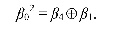
- Therefore, computing β2 over GF(25) with a generator polynomial of α5 + α2 + 1 requires three 2-input Exclusive-OR functions. If implemented in a field programmable gate array (FPGA), a total of three logic elements (look up tables, or LUTS) would be required to perform the operation.
-
Figs. 4B-4D show the logic diagrams for the remaining required β2m operations, namely, the β4, β8, and β16exponential generators Fig 3 , respectively, for this polynomial generator example. More specifically, the β4exponential generator 304 shown inFig. 4B maps the input bits of an element β into the output bits of β4. In accordance with equation (9), β4 = θ4 x β. For the matrix θ4 given above for this generator polynomial, the bits of β4 are determined as:


and
- The β8
exponential generator 306 shown inFig. 4C maps the input bits of an element β into the output bits of β8. In accordance with equation (9), β8 = θ8 x β. For the matrix θ8 given above for this generator polynomial, the bits of β8 are determined as:


and
- The β16
exponential generator 308 shown inFig. 4D maps the input bits of an element β into the output bits of β16. In accordance with equation (9), β16 = θ16 x β. For the matrix θ16 given above for this generator polynomial, the bits of β16 are determined as:


and
- Examining the remaining β2m operators, a total of 23 2-input exclusive-OR functions are required to perform all the field exponentiation operations β2, β4, β8, and β16. Even fewer are required if certain redundancy is eliminated. For example, two of the two-input exclusive-OR functions of the β4 exponentiation circuit 304 shown in
Fig. 4B have the same inputs β3 and β4. Instead, a single exclusive-OR function could be used whose output is used both as the output β1 4 and as an input to another two-input exclusive-OR function along with β2 to produce β3 4 . Ignoring the savings gained by eliminating such redundancy, the total number of exclusive-OR operations required to generate the exponential values in this example is broken down in Table 1.Table 1: Galois field Exponentiation Function Requirements Value Exclusive-OR Functions FPGA LUTs β2 3 3 β4 7 5 β 88 5 β16 5 3 Total 23 16 - By way of comparison, a full Galois multiplier requires 19 2-input Exclusive-OR functions and 16 2-input logical AND functions. Thus, all the exponentiation operations required to perform a multiplicative inversion occur in approximately one-third the size of a single Galois field multiplier.
- The multi-stage serial squaring-and-multiplying techniques illustrated in
Figs. 1 and 2 are convenient from the standpoint that a standard multiplier circuit can be used to carry out both the squaring and multiplication operations (the squaring operation involves multiplying an input by itself), and the multiplicative inverse of a finite field element can be computed by stringing together a number of such multiplier circuits in a multi-stage configuration. - A unique aspect of the technique described herein is that the 2 m powers of a finite field element are computed in a more elegant and efficient manner without the use of multipliers or look-up tables that implement multiplication operations. Rather, the technique is based on the insight that there is actually a combinatorial way to represent the 2 m powers of a finite field element which is much simpler and can be implemented in parallel.
- The expression in equation (8) is important in understanding how exponentiation circuits can be constructed with relatively few components and/or operations. In effect, as higher orders of β are computed, the cross-products keep disappearing (canceling out) such that the computations do not become more complex even at higher powers of β. This characteristic permits the relationships between β and the powers of β to be represented in a simple n x n exponentiation matrix which transforms the digits (in this case bits) of β to digits (bits) of the output power of β (β2m ). The exponentiation matrix can be implemented using only combinatory logic, where each bit of the output exponential β2m is either equal to the value of one of the input bits of β or an exclusive-OR combination of certain bits of β. This is because, by its nature, the exponentiation matrix yields summations of input bits, which are performed logically as an exclusive-OR operation. As used herein and in the claims the terms combinatory logic and combinatory logic circuits refer to circuitry (implemented in hardware, software, look-up tables, or combinations thereof) that maps input digits to output digits based on only logical relationships. These logical relationships include mapping logical combinations of certain input digits of an input field element to output digits of the output field element. These logical relationships may also include the direct mapping of an input digit to an output digit in some instances, as shown for example with the direct mapping of input bit β2 to output bit β4 2 in
exponentiation circuit 302 inFig. 4A . All of the logical combinations employed by the combinatory logic are exclusive-OR combinations of the input digits. -
Fig. 5 is a flow diagram summarizing the operations performed to carry out exponentiation of a finite field element and computation of the multiplicative inverse of a field element in accordance with an embodiment of the invention. Inoperation 510, a multi-digit field element β of a finite field is supplied to each of a plurality of parallel exponentiation circuits. Inoperation 520, each of the exponentiation circuits essentially maps the digits of the input field element β to output digits of an output multi-digit field element β2m , which is a 2 m power of the input field element β, where m is an integer greater than zero and where the value of m is different for each exponentiation circuit. This mapping is accomplished using combinatory logic circuits. Inoperation 530, the output multi-digit field elements β2m from each of the parallel exponentiation circuits are multiplied together to generate the multiplicative inverse of the field element β. - Although not applicable to the subject of Galois field inversion, the matrix algebra approach used to derive the exponentiation matrices also applies to multiplying a Galois field value by a constant α N :

where
- Continuing with the example of a field over GF(25) with a generator polynomial of α5 + α2 + 1 (001012), multiplying a field value by α7 would be computed as follows:

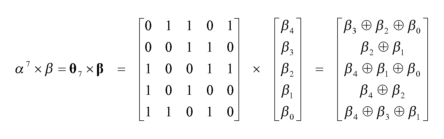
- Therefore, computing α7 × β over GF(25) with a generator polynomial of α5 + α2 + 1 requires eight 2-input exclusive-OR functions. This array maps into the digital logic circuit shown in
Fig. 6 . If implemented in an FPGA, a total of five LUTs would be required to perform the operation. - Taking into consideration this extension of multiplying a finite field element by a constant, it will be appreciated that the invention encompasses the use of matrix algebra with finite field elements, resulting in arrays that are summations of input values that can be used to raise a field element to a power or to carry out multiplication by a constant.
- The invention can be used in any hardware or software application that requires finite field arithmetic, such as encryption or forward error correction algorithms. As previously described, forward error correction codes are used extensively in communications to ensure the accuracy of data being received. Properly encoding data with finite field arithmetic allows a relatively small check word to be used to check the accuracy of a large amount of data and to determine which data is erroneous. Using the techniques of the present invention, the computations required to perform these types of operations can be carried out with less hardware and/or less and faster processing.
- Having described preferred embodiments of circuits and methods for performing exponentiation and inversion of finite field elements, it is believed that other modifications, variations and changes will be suggested to those skilled in the art in view of the teachings set forth herein. It is therefore to be understood that all such variations, modifications and changes are believed to fall within the scope of the present invention as defined by the appended claims. Although specific terms are employed herein, they are used in a generic and descriptive sense only and not for purposes of limitation.
Claims (15)
- An exponentiation circuit for computing an exponential power of a finite field element, comprising:combinatory logic circuits configured to receive input digits of a multi-digit field element β of a finite field, the combinatory logic circuits mapping the input digits to output digits of an output multi-digit field element β2m , where m is an integer greater than zero.
- The circuit of claim 1, wherein at least some of the output digits are generated by the combinatory logic circuits as logical combinations of certain input digits and at least some of the output digits are generated by the combinatory logic circuits from only one of the input digits by directly mapping an input digit to an output digit.
- The circuit of claim 1 or 2, wherein the exponentiation circuit does not perform any multiplication operations.
- The circuit of one of the preceding claims, wherein logical combinations generated by the combinatory logic circuits include only exclusive-OR combinations.
- The circuit of one of the preceding claims, wherein the combinatory logic circuits implement logical relationships between the field element β and the output field element β2m specified by an exponentiation matrix, and in particular wherein the exponentiation matrix implemented by the combinatory logic circuits is an n x n matrix equal to the transform of the first n elements of the finite field raised to the 2 m power, where n is the number of digits of the multi-digit field element β.
- A circuit for generating a multiplicative inverse of a finite field element, comprising:a plurality of parallel exponentiation circuits, each of the parallel exponentiation circuits receiving a multi-digit field element β, preferably a multi-bit binary field element, and generating an output multi-digit field element β2m , where m is an integer greater than zero;a plurality of multiplier circuits configured to multiply together outputs of the parallel exponentiation circuits to generate the multiplicative inverse of the field element β.
- The circuit of claim 6, wherein the parallel exponentiation circuits- do not perform any multiplication operations; and/or- generate exponential powers of the field element β using only combinatory logic on the digits of the field element β, and in particular wherein the combinatory logic- includes only exclusive-OR combinations; and/or- implements logical relationships between the field element β and the output field element β2m specified by an exponentiation matrix.
- The circuit of claim 6 or 7, wherein each of the exponentiation circuits is implement with at least one of: a look-up table; a plurality of exclusive-OR gates; and software.
- A circuit for multiplying a finite field element by a constant, comprising:combinatory logic circuits configured to receive input digits of a multi-digit field element β of a finite field, the combinatory logic circuits mapping the input digits to output digits of an output multi-digit field element α n x β, where α n is a constant and n is an integer greater than zero.
- A method for generating an exponential power of a finite field element, comprising:receiving input digits of a multi-digit field element β of α finite field at an exponentiation circuit;mapping via combinatory logic circuits the input digits to output digits of an output multi-digit field element β2m , where m is an integer greater than zero; and supplying the output multi-digit field element β2m as an output of the exponentiation circuit.
- The method of claim 10, wherein at least some of the output digits are generated by the combinatory logic circuits as logical combinations of certain input digits and at least some of the output digits are generated by the combinatory logic circuits from only one of the input digits by directly mapping an input digit to an output digit.
- The method of claim 10 or 11, wherein the method is carried out without performing any multiplication operations.
- The method of one of claims 10 to 12, wherein logical combinations include only exclusive-OR combinations.
- The method of one of claims 10 to 13, wherein the method implements, via the combinatory logic circuits, logical relationships between the field element β and the output field element β2m specified by an exponentiation matrix.
- The method of one of claims 10 to 14, further comprising:receiving the multi-digit field element β at a plurality of parallel exponentiation circuits, each of the parallel exponentiation circuits generating an output multi-digit field element β2m for a different value of m; andmultiplying together outputs of the parallel exponentiation circuits to generate the multiplicative inverse of the field element β.
Applications Claiming Priority (1)
| Application Number | Priority Date | Filing Date | Title |
|---|---|---|---|
| US12/476,389 US8443028B2 (en) | 2009-06-02 | 2009-06-02 | Circuits and methods for performing exponentiation and inversion of finite field elements |
Publications (4)
| Publication Number | Publication Date |
|---|---|
| EP2261795A1 true EP2261795A1 (en) | 2010-12-15 |
| EP2261795B1 EP2261795B1 (en) | 2011-11-23 |
| EP2261795B8 EP2261795B8 (en) | 2012-05-02 |
| EP2261795B9 EP2261795B9 (en) | 2012-05-09 |
Family
ID=42359487
Family Applications (1)
| Application Number | Title | Priority Date | Filing Date |
|---|---|---|---|
| EP10161704A Not-in-force EP2261795B9 (en) | 2009-06-02 | 2010-05-03 | Circuits and methods for performing exponentiation and inversion of finite field elements |
Country Status (3)
| Country | Link |
|---|---|
| US (1) | US8443028B2 (en) |
| EP (1) | EP2261795B9 (en) |
| AT (1) | ATE534950T1 (en) |
Cited By (1)
| Publication number | Priority date | Publication date | Assignee | Title |
|---|---|---|---|---|
| CN104536943A (en) * | 2015-01-13 | 2015-04-22 | 江苏中兴微通信息科技有限公司 | Low-division-quantity fixed point implementation method and device for matrix inversion |
Families Citing this family (11)
| Publication number | Priority date | Publication date | Assignee | Title |
|---|---|---|---|---|
| US11093213B1 (en) | 2010-12-29 | 2021-08-17 | Ternarylogic Llc | Cryptographic computer machines with novel switching devices |
| US9141131B2 (en) * | 2011-08-26 | 2015-09-22 | Cognitive Electronics, Inc. | Methods and systems for performing exponentiation in a parallel processing environment |
| CN102902510B (en) * | 2012-08-03 | 2016-04-13 | 华南理工大学 | A kind of finite field inverter |
| US9025766B2 (en) * | 2013-03-13 | 2015-05-05 | Intel Corporation | Efficient hardware architecture for a S1 S-box in a ZUC cipher |
| US9804828B2 (en) | 2014-11-24 | 2017-10-31 | Apple Inc. | Cubic root of a galois field element |
| US9473176B2 (en) * | 2014-11-27 | 2016-10-18 | Apple Inc. | Implementation of log and inverse operation in a Galois Field |
| US12143468B2 (en) | 2015-12-20 | 2024-11-12 | Lcip Jv | Cryptographic computer machines with novel switching devices |
| US12425189B1 (en) | 2015-12-20 | 2025-09-23 | Peter Lablans | Cryptographic computer machines with novel switching devices |
| US10409615B2 (en) * | 2017-06-19 | 2019-09-10 | The Regents Of The University Of Michigan | Configurable arithmetic unit |
| US11032061B2 (en) * | 2018-04-27 | 2021-06-08 | Microsoft Technology Licensing, Llc | Enabling constant plaintext space in bootstrapping in fully homomorphic encryption |
| CN114595486B (en) * | 2022-05-10 | 2022-08-05 | 深圳佰维存储科技股份有限公司 | Zero data identification method and device, readable storage medium and electronic equipment |
Citations (1)
| Publication number | Priority date | Publication date | Assignee | Title |
|---|---|---|---|---|
| US20020032711A1 (en) * | 2000-06-21 | 2002-03-14 | Sumio Morioka | Multiplication module, multiplicative inverse arithmetic circuit, multiplicative inverse arithmetic control method, apparatus employing multiplicative inverse arithmetic circuit, and cryptographic apparatus and error correction decoder therefor |
Family Cites Families (4)
| Publication number | Priority date | Publication date | Assignee | Title |
|---|---|---|---|---|
| US5812438A (en) * | 1995-10-12 | 1998-09-22 | Adaptec, Inc. | Arithmetic logic unit and method for numerical computations in galois fields |
| FR2754616B1 (en) | 1996-10-11 | 1998-12-04 | Sgs Thomson Microelectronics | METHOD AND CIRCUIT FOR DIVIDING ELEMENTS OF A WALL BODY |
| KR100304193B1 (en) * | 1998-02-06 | 2001-11-22 | 윤종용 | Inverse circuit of reed-solomon decoder |
| US6779011B2 (en) * | 2001-02-28 | 2004-08-17 | Maxtor Corporation | System for performing multiplication and division in GF(22M) |
-
2009
- 2009-06-02 US US12/476,389 patent/US8443028B2/en not_active Expired - Fee Related
-
2010
- 2010-05-03 AT AT10161704T patent/ATE534950T1/en active
- 2010-05-03 EP EP10161704A patent/EP2261795B9/en not_active Not-in-force
Patent Citations (1)
| Publication number | Priority date | Publication date | Assignee | Title |
|---|---|---|---|---|
| US20020032711A1 (en) * | 2000-06-21 | 2002-03-14 | Sumio Morioka | Multiplication module, multiplicative inverse arithmetic circuit, multiplicative inverse arithmetic control method, apparatus employing multiplicative inverse arithmetic circuit, and cryptographic apparatus and error correction decoder therefor |
Non-Patent Citations (2)
| Title |
|---|
| CHOOMCHUAY S: "On the Implementation of Finite Field Operations", LADKRABANG ENGINEERING JOURNAL, TH, vol. 11, no. 1, 1 June 1994 (1994-06-01), pages 7 - 16, XP007914787 * |
| JORGE GUAJARDO ET AL: "Efficient Hardware Implementation of Finite Fields with Applications to Cryptography", ACTA APPLICANDAE MATHEMATICAE, KLUWER ACADEMIC PUBLISHERS, DO LNKD- DOI:10.1007/S10440-006-9072-Z, vol. 93, no. 1-3, 26 September 2006 (2006-09-26), pages 75 - 118, XP019432733, ISSN: 1572-9036 * |
Cited By (2)
| Publication number | Priority date | Publication date | Assignee | Title |
|---|---|---|---|---|
| CN104536943A (en) * | 2015-01-13 | 2015-04-22 | 江苏中兴微通信息科技有限公司 | Low-division-quantity fixed point implementation method and device for matrix inversion |
| CN104536943B (en) * | 2015-01-13 | 2017-08-29 | 江苏中兴微通信息科技有限公司 | A kind of matrix inversion fixed-point implementation method and device of low division amount |
Also Published As
| Publication number | Publication date |
|---|---|
| EP2261795B9 (en) | 2012-05-09 |
| ATE534950T1 (en) | 2011-12-15 |
| US20100306299A1 (en) | 2010-12-02 |
| EP2261795B8 (en) | 2012-05-02 |
| EP2261795B1 (en) | 2011-11-23 |
| US8443028B2 (en) | 2013-05-14 |
Similar Documents
| Publication | Publication Date | Title |
|---|---|---|
| EP2261795B9 (en) | Circuits and methods for performing exponentiation and inversion of finite field elements | |
| Rodríguez-Henríquez et al. | Cryptographic algorithms on reconfigurable hardware | |
| Cantor et al. | On fast multiplication of polynomials over arbitrary algebras | |
| US6760742B1 (en) | Multi-dimensional galois field multiplier | |
| von zur Gathen et al. | Efficient FPGA-based Karatsuba multipliers for polynomials over | |
| US20110246548A1 (en) | Sequential galois field multiplication architecture and method | |
| Erdem et al. | Polynomial basis multiplication over GF (2m) | |
| EP0741355A1 (en) | Finite field multiple bit multiplier | |
| Djath et al. | Hierarchical approach in RNS base extension for asymmetric cryptography | |
| Reyhani-Masoleh | A new bit-serial architecture for field multiplication using polynomial bases | |
| US20170026178A1 (en) | Computational method, computational device andcomputer software product for montgomery domain | |
| Daneshbeh et al. | A class of unidirectional bit serial systolic architectures for multiplicative inversion and division over GF (2/sup m/) | |
| US6662201B1 (en) | Modular arithmetic apparatus and method having high-speed base conversion function | |
| US20040177105A1 (en) | Multilplier and cipher circuit | |
| Bhaskar et al. | An efficient hardware model for RSA Encryption system using Vedic mathematics | |
| Namin et al. | A word-level finite field multiplier using normal basis | |
| KR100670780B1 (en) | Hybrid Multiplication Computing Device and Method in Finite Field | |
| JP2002023999A (en) | Multiplication module, multiplicative inverse operation circuit, multiplicative inverse operation control method, device using the multiplicative inverse operation, encryption device, error correction decoder | |
| KR100480997B1 (en) | APPARATUS OF FIELD MULTIPLICATION OVER GF(p) AND GF(2^m) | |
| Wang et al. | An efficient and parallelism-scalable large integer multiplier architecture using least-positive form and winograd fast algorithm | |
| EP2434650A1 (en) | Reed-Solomon encoder with simplified Galois field multipliers | |
| Bharathwaj et al. | An alternate approach to modular multiplication for finite fields [GF (2/sup m/)] using Itoh Tsujii algorithm | |
| Smirnov | A bilinear algorithm of length 22 for approximate multiplication of 2× 7 and 7× 2 matrices | |
| Kerins et al. | Fully paramaterisable galois field arithmetic processor over GF (3m) suitable for elliptic curve cryptography | |
| Zhang et al. | Efficient and Flexible Differet-Radix Montgomery Modular Multiplication for Hardware Implementation |
Legal Events
| Date | Code | Title | Description |
|---|---|---|---|
| PUAI | Public reference made under article 153(3) epc to a published international application that has entered the european phase |
Free format text: ORIGINAL CODE: 0009012 |
|
| AK | Designated contracting states |
Kind code of ref document: A1 Designated state(s): AL AT BE BG CH CY CZ DE DK EE ES FI FR GB GR HR HU IE IS IT LI LT LU LV MC MK MT NL NO PL PT RO SE SI SK SM TR |
|
| AX | Request for extension of the european patent |
Extension state: BA ME RS |
|
| 17P | Request for examination filed |
Effective date: 20110113 |
|
| GRAP | Despatch of communication of intention to grant a patent |
Free format text: ORIGINAL CODE: EPIDOSNIGR1 |
|
| RIC1 | Information provided on ipc code assigned before grant |
Ipc: G06F 7/72 20060101AFI20110512BHEP |
|
| GRAS | Grant fee paid |
Free format text: ORIGINAL CODE: EPIDOSNIGR3 |
|
| GRAA | (expected) grant |
Free format text: ORIGINAL CODE: 0009210 |
|
| AK | Designated contracting states |
Kind code of ref document: B1 Designated state(s): AL AT BE BG CH CY CZ DE DK EE ES FI FR GB GR HR HU IE IS IT LI LT LU LV MC MK MT NL NO PL PT RO SE SI SK SM TR |
|
| REG | Reference to a national code |
Ref country code: GB Ref legal event code: FG4D |
|
| REG | Reference to a national code |
Ref country code: CH Ref legal event code: EP |
|
| REG | Reference to a national code |
Ref country code: IE Ref legal event code: FG4D |
|
| REG | Reference to a national code |
Ref country code: DE Ref legal event code: R096 Ref document number: 602010000441 Country of ref document: DE Effective date: 20120119 |
|
| REG | Reference to a national code |
Ref country code: NL Ref legal event code: VDEP Effective date: 20111123 |
|
| LTIE | Lt: invalidation of european patent or patent extension |
Effective date: 20111123 |
|
| PG25 | Lapsed in a contracting state [announced via postgrant information from national office to epo] |
Ref country code: NO Free format text: LAPSE BECAUSE OF FAILURE TO SUBMIT A TRANSLATION OF THE DESCRIPTION OR TO PAY THE FEE WITHIN THE PRESCRIBED TIME-LIMIT Effective date: 20120223 Ref country code: IS Free format text: LAPSE BECAUSE OF FAILURE TO SUBMIT A TRANSLATION OF THE DESCRIPTION OR TO PAY THE FEE WITHIN THE PRESCRIBED TIME-LIMIT Effective date: 20120323 Ref country code: LT Free format text: LAPSE BECAUSE OF FAILURE TO SUBMIT A TRANSLATION OF THE DESCRIPTION OR TO PAY THE FEE WITHIN THE PRESCRIBED TIME-LIMIT Effective date: 20111123 |
|
| PG25 | Lapsed in a contracting state [announced via postgrant information from national office to epo] |
Ref country code: SI Free format text: LAPSE BECAUSE OF FAILURE TO SUBMIT A TRANSLATION OF THE DESCRIPTION OR TO PAY THE FEE WITHIN THE PRESCRIBED TIME-LIMIT Effective date: 20111123 Ref country code: GR Free format text: LAPSE BECAUSE OF FAILURE TO SUBMIT A TRANSLATION OF THE DESCRIPTION OR TO PAY THE FEE WITHIN THE PRESCRIBED TIME-LIMIT Effective date: 20120224 Ref country code: LV Free format text: LAPSE BECAUSE OF FAILURE TO SUBMIT A TRANSLATION OF THE DESCRIPTION OR TO PAY THE FEE WITHIN THE PRESCRIBED TIME-LIMIT Effective date: 20111123 Ref country code: SE Free format text: LAPSE BECAUSE OF FAILURE TO SUBMIT A TRANSLATION OF THE DESCRIPTION OR TO PAY THE FEE WITHIN THE PRESCRIBED TIME-LIMIT Effective date: 20111123 Ref country code: PT Free format text: LAPSE BECAUSE OF FAILURE TO SUBMIT A TRANSLATION OF THE DESCRIPTION OR TO PAY THE FEE WITHIN THE PRESCRIBED TIME-LIMIT Effective date: 20120323 Ref country code: HR Free format text: LAPSE BECAUSE OF FAILURE TO SUBMIT A TRANSLATION OF THE DESCRIPTION OR TO PAY THE FEE WITHIN THE PRESCRIBED TIME-LIMIT Effective date: 20111123 Ref country code: NL Free format text: LAPSE BECAUSE OF FAILURE TO SUBMIT A TRANSLATION OF THE DESCRIPTION OR TO PAY THE FEE WITHIN THE PRESCRIBED TIME-LIMIT Effective date: 20111123 Ref country code: BE Free format text: LAPSE BECAUSE OF FAILURE TO SUBMIT A TRANSLATION OF THE DESCRIPTION OR TO PAY THE FEE WITHIN THE PRESCRIBED TIME-LIMIT Effective date: 20111123 |
|
| PG25 | Lapsed in a contracting state [announced via postgrant information from national office to epo] |
Ref country code: CY Free format text: LAPSE BECAUSE OF FAILURE TO SUBMIT A TRANSLATION OF THE DESCRIPTION OR TO PAY THE FEE WITHIN THE PRESCRIBED TIME-LIMIT Effective date: 20111123 |
|
| PG25 | Lapsed in a contracting state [announced via postgrant information from national office to epo] |
Ref country code: DK Free format text: LAPSE BECAUSE OF FAILURE TO SUBMIT A TRANSLATION OF THE DESCRIPTION OR TO PAY THE FEE WITHIN THE PRESCRIBED TIME-LIMIT Effective date: 20111123 Ref country code: EE Free format text: LAPSE BECAUSE OF FAILURE TO SUBMIT A TRANSLATION OF THE DESCRIPTION OR TO PAY THE FEE WITHIN THE PRESCRIBED TIME-LIMIT Effective date: 20111123 Ref country code: BG Free format text: LAPSE BECAUSE OF FAILURE TO SUBMIT A TRANSLATION OF THE DESCRIPTION OR TO PAY THE FEE WITHIN THE PRESCRIBED TIME-LIMIT Effective date: 20120223 Ref country code: SK Free format text: LAPSE BECAUSE OF FAILURE TO SUBMIT A TRANSLATION OF THE DESCRIPTION OR TO PAY THE FEE WITHIN THE PRESCRIBED TIME-LIMIT Effective date: 20111123 Ref country code: CZ Free format text: LAPSE BECAUSE OF FAILURE TO SUBMIT A TRANSLATION OF THE DESCRIPTION OR TO PAY THE FEE WITHIN THE PRESCRIBED TIME-LIMIT Effective date: 20111123 |
|
| REG | Reference to a national code |
Ref country code: DE Ref legal event code: R097 Ref document number: 602010000441 Country of ref document: DE |
|
| PG25 | Lapsed in a contracting state [announced via postgrant information from national office to epo] |
Ref country code: RO Free format text: LAPSE BECAUSE OF FAILURE TO SUBMIT A TRANSLATION OF THE DESCRIPTION OR TO PAY THE FEE WITHIN THE PRESCRIBED TIME-LIMIT Effective date: 20111123 Ref country code: PL Free format text: LAPSE BECAUSE OF FAILURE TO SUBMIT A TRANSLATION OF THE DESCRIPTION OR TO PAY THE FEE WITHIN THE PRESCRIBED TIME-LIMIT Effective date: 20111123 |
|
| PLBE | No opposition filed within time limit |
Free format text: ORIGINAL CODE: 0009261 |
|
| STAA | Information on the status of an ep patent application or granted ep patent |
Free format text: STATUS: NO OPPOSITION FILED WITHIN TIME LIMIT |
|
| REG | Reference to a national code |
Ref country code: GB Ref legal event code: 732E Free format text: REGISTERED BETWEEN 20120906 AND 20120912 |
|
| REG | Reference to a national code |
Ref country code: FR Ref legal event code: TP Owner name: EXELIS INC., US Effective date: 20120912 Ref country code: FR Ref legal event code: CD Owner name: EXELIS INC., US Effective date: 20120912 |
|
| 26N | No opposition filed |
Effective date: 20120824 |
|
| REG | Reference to a national code |
Ref country code: DE Ref legal event code: R082 Ref document number: 602010000441 Country of ref document: DE Representative=s name: DREISS PATENTANWAELTE PARTNERSCHAFT, DE Effective date: 20120913 Ref country code: DE Ref legal event code: R081 Ref document number: 602010000441 Country of ref document: DE Owner name: EXELIS INC., US Free format text: FORMER OWNER: ITT MANUFACTURING ENTERPRISES, INC., WILMINGTON, US Effective date: 20120913 Ref country code: DE Ref legal event code: R081 Ref document number: 602010000441 Country of ref document: DE Owner name: EXELIS INC., MCLEAN, US Free format text: FORMER OWNER: ITT MANUFACTURING ENTERPRISES, INC., WILMINGTON, DEL., US Effective date: 20120913 Ref country code: DE Ref legal event code: R082 Ref document number: 602010000441 Country of ref document: DE Representative=s name: DREISS PATENTANWAELTE PARTG MBB, DE Effective date: 20120913 Ref country code: DE Ref legal event code: R082 Ref document number: 602010000441 Country of ref document: DE Representative=s name: PATENTANWAELTE MAGENBAUER & KOLLEGEN, DE Effective date: 20120913 Ref country code: DE Ref legal event code: R082 Ref document number: 602010000441 Country of ref document: DE Representative=s name: PATENTANWAELTE MAGENBAUER & KOLLEGEN PARTNERSC, DE Effective date: 20120913 |
|
| REG | Reference to a national code |
Ref country code: AT Ref legal event code: MK05 Ref document number: 534950 Country of ref document: AT Kind code of ref document: T Effective date: 20111123 |
|
| REG | Reference to a national code |
Ref country code: DE Ref legal event code: R097 Ref document number: 602010000441 Country of ref document: DE Effective date: 20120824 |
|
| PG25 | Lapsed in a contracting state [announced via postgrant information from national office to epo] |
Ref country code: MC Free format text: LAPSE BECAUSE OF NON-PAYMENT OF DUE FEES Effective date: 20120531 |
|
| PG25 | Lapsed in a contracting state [announced via postgrant information from national office to epo] |
Ref country code: AT Free format text: LAPSE BECAUSE OF FAILURE TO SUBMIT A TRANSLATION OF THE DESCRIPTION OR TO PAY THE FEE WITHIN THE PRESCRIBED TIME-LIMIT Effective date: 20111123 |
|
| REG | Reference to a national code |
Ref country code: IE Ref legal event code: MM4A |
|
| PG25 | Lapsed in a contracting state [announced via postgrant information from national office to epo] |
Ref country code: MK Free format text: LAPSE BECAUSE OF FAILURE TO SUBMIT A TRANSLATION OF THE DESCRIPTION OR TO PAY THE FEE WITHIN THE PRESCRIBED TIME-LIMIT Effective date: 20111123 |
|
| PG25 | Lapsed in a contracting state [announced via postgrant information from national office to epo] |
Ref country code: ES Free format text: LAPSE BECAUSE OF FAILURE TO SUBMIT A TRANSLATION OF THE DESCRIPTION OR TO PAY THE FEE WITHIN THE PRESCRIBED TIME-LIMIT Effective date: 20120305 Ref country code: IE Free format text: LAPSE BECAUSE OF NON-PAYMENT OF DUE FEES Effective date: 20120503 |
|
| PG25 | Lapsed in a contracting state [announced via postgrant information from national office to epo] |
Ref country code: FI Free format text: LAPSE BECAUSE OF FAILURE TO SUBMIT A TRANSLATION OF THE DESCRIPTION OR TO PAY THE FEE WITHIN THE PRESCRIBED TIME-LIMIT Effective date: 20111123 |
|
| PG25 | Lapsed in a contracting state [announced via postgrant information from national office to epo] |
Ref country code: MT Free format text: LAPSE BECAUSE OF FAILURE TO SUBMIT A TRANSLATION OF THE DESCRIPTION OR TO PAY THE FEE WITHIN THE PRESCRIBED TIME-LIMIT Effective date: 20111123 |
|
| PGFP | Annual fee paid to national office [announced via postgrant information from national office to epo] |
Ref country code: IT Payment date: 20130531 Year of fee payment: 4 |
|
| PG25 | Lapsed in a contracting state [announced via postgrant information from national office to epo] |
Ref country code: AL Free format text: LAPSE BECAUSE OF FAILURE TO SUBMIT A TRANSLATION OF THE DESCRIPTION OR TO PAY THE FEE WITHIN THE PRESCRIBED TIME-LIMIT Effective date: 20111123 |
|
| PG25 | Lapsed in a contracting state [announced via postgrant information from national office to epo] |
Ref country code: TR Free format text: LAPSE BECAUSE OF FAILURE TO SUBMIT A TRANSLATION OF THE DESCRIPTION OR TO PAY THE FEE WITHIN THE PRESCRIBED TIME-LIMIT Effective date: 20111123 |
|
| PG25 | Lapsed in a contracting state [announced via postgrant information from national office to epo] |
Ref country code: LU Free format text: LAPSE BECAUSE OF NON-PAYMENT OF DUE FEES Effective date: 20120503 Ref country code: SM Free format text: LAPSE BECAUSE OF FAILURE TO SUBMIT A TRANSLATION OF THE DESCRIPTION OR TO PAY THE FEE WITHIN THE PRESCRIBED TIME-LIMIT Effective date: 20111123 |
|
| PG25 | Lapsed in a contracting state [announced via postgrant information from national office to epo] |
Ref country code: HU Free format text: LAPSE BECAUSE OF FAILURE TO SUBMIT A TRANSLATION OF THE DESCRIPTION OR TO PAY THE FEE WITHIN THE PRESCRIBED TIME-LIMIT Effective date: 20100503 |
|
| REG | Reference to a national code |
Ref country code: DE Ref legal event code: R082 Ref document number: 602010000441 Country of ref document: DE Representative=s name: PATENTANWAELTE MAGENBAUER & KOLLEGEN, DE Ref country code: DE Ref legal event code: R082 Ref document number: 602010000441 Country of ref document: DE Representative=s name: PATENTANWAELTE MAGENBAUER & KOLLEGEN PARTNERSC, DE |
|
| REG | Reference to a national code |
Ref country code: CH Ref legal event code: PL |
|
| GBPC | Gb: european patent ceased through non-payment of renewal fee |
Effective date: 20140503 |
|
| PG25 | Lapsed in a contracting state [announced via postgrant information from national office to epo] |
Ref country code: LI Free format text: LAPSE BECAUSE OF NON-PAYMENT OF DUE FEES Effective date: 20140531 Ref country code: CH Free format text: LAPSE BECAUSE OF NON-PAYMENT OF DUE FEES Effective date: 20140531 |
|
| PG25 | Lapsed in a contracting state [announced via postgrant information from national office to epo] |
Ref country code: IT Free format text: LAPSE BECAUSE OF NON-PAYMENT OF DUE FEES Effective date: 20140503 |
|
| REG | Reference to a national code |
Ref country code: FR Ref legal event code: PLFP Year of fee payment: 6 |
|
| PG25 | Lapsed in a contracting state [announced via postgrant information from national office to epo] |
Ref country code: GB Free format text: LAPSE BECAUSE OF NON-PAYMENT OF DUE FEES Effective date: 20140503 |
|
| REG | Reference to a national code |
Ref country code: FR Ref legal event code: PLFP Year of fee payment: 7 |
|
| PGFP | Annual fee paid to national office [announced via postgrant information from national office to epo] |
Ref country code: DE Payment date: 20160527 Year of fee payment: 7 |
|
| PGFP | Annual fee paid to national office [announced via postgrant information from national office to epo] |
Ref country code: FR Payment date: 20160530 Year of fee payment: 7 |
|
| REG | Reference to a national code |
Ref country code: DE Ref legal event code: R119 Ref document number: 602010000441 Country of ref document: DE |
|
| REG | Reference to a national code |
Ref country code: FR Ref legal event code: ST Effective date: 20180131 |
|
| PG25 | Lapsed in a contracting state [announced via postgrant information from national office to epo] |
Ref country code: DE Free format text: LAPSE BECAUSE OF NON-PAYMENT OF DUE FEES Effective date: 20171201 |
|
| PG25 | Lapsed in a contracting state [announced via postgrant information from national office to epo] |
Ref country code: FR Free format text: LAPSE BECAUSE OF NON-PAYMENT OF DUE FEES Effective date: 20170531 |