EP2259161A2 - Voltage and current regulators with switched output capacitors for multiple regulation states - Google Patents
Voltage and current regulators with switched output capacitors for multiple regulation states Download PDFInfo
- Publication number
- EP2259161A2 EP2259161A2 EP10160094A EP10160094A EP2259161A2 EP 2259161 A2 EP2259161 A2 EP 2259161A2 EP 10160094 A EP10160094 A EP 10160094A EP 10160094 A EP10160094 A EP 10160094A EP 2259161 A2 EP2259161 A2 EP 2259161A2
- Authority
- EP
- European Patent Office
- Prior art keywords
- regulator
- load
- output
- voltage
- capacitor
- Prior art date
- Legal status (The legal status is an assumption and is not a legal conclusion. Google has not performed a legal analysis and makes no representation as to the accuracy of the status listed.)
- Granted
Links
Images


Classifications
-
- G—PHYSICS
- G05—CONTROLLING; REGULATING
- G05F—SYSTEMS FOR REGULATING ELECTRIC OR MAGNETIC VARIABLES
- G05F1/00—Automatic systems in which deviations of an electric quantity from one or more predetermined values are detected at the output of the system and fed back to a device within the system to restore the detected quantity to its predetermined value or values, i.e. retroactive systems
- G05F1/10—Regulating voltage or current
- G05F1/46—Regulating voltage or current wherein the variable actually regulated by the final control device is DC
- G05F1/56—Regulating voltage or current wherein the variable actually regulated by the final control device is DC using semiconductor devices in series with the load as final control devices
Definitions
- the disclosure relates generally to voltage and current regulators, and more specifically to regulators using switchable output capacitors for improving the output voltage response time of regulators when switching from one regulation state to another.
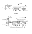
- the typical current or voltage regulator 10 includes regulator control circuit 12 and a control loop or feedback network 14 for regulating the output 22 provided to the load 16.
- the voltage output of the regulator 10 is usually set by a reference signal (current or voltage) S REF indicated at 18, while the output of the regulator 10 is typically bypassed with a single large capacitor 20.
- S REF reference signal
- the large output capacitor 20 must be charged or discharged to achieve the new regulation voltage V OUT . This causes the transition time between states to be excessively long and impractical for applications where the transition times must be less than several micro seconds.
- the large output capacitor 20 thus directly limits the step-response of the regulator's control loop.
- the reference signal S REF is changed at the input 18.
- the slew-rate of the output V out at 22 is limited to the current sinking or sourcing capabilities of the regulator 12, the impedance of the load 16, the size of the output capacitor 20, and the bandwidth of the regulator's control loop 14.
- the rise-time or decay time of the output may be limited from tens to hundreds of microseconds. This may be acceptable for systems where a single regulation state is desired, but can be unacceptable where the regulator is designed to operate in any one of a plurality of regulation states. It is desirable to provide a solution to allow a very fast response time to change from one regulation state to another without redesigning the control-loop, changing the bandwidth of the control-loop, or reducing the size of the output capacitor.
- FIG. 1 is a generalized partial block and partial schematic diagram of a typical current or voltage regulator including a single bypass capacitor;
- FIG. 2 is a generalized partial block and partial schematic diagram of one embodiment of a current or voltage regulator employing a plurality of bypass capacitors for use in operating in any one of a plurality of regulation states;
- FIG. 3 is a generalized partial block and partial schematic diagram of another embodiment of a current or voltage regulator employing a plurality of bypass capacitors for use in operating in any one of a plurality of regulation states;
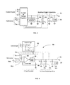
- FIG. 4 is a generalized partial block and partial schematic diagram of the embodiment of FIG. 2 , further showing more details of the control logic and an error amplifier;
- FIG. 5 is a generalized partial block and partial schematic diagram of a current regulator, further showing more details of the application of control signals for controlling the plurality of bypass capacitors;
- FIG. 6 is a generalized partial block and partial schematic diagram of the embodiment of FIG. 2 , further showing more details of the control logic and a plurality of error amplifiers;
- FIG. 7 is a graphical illustration of an exemplary response of a current or voltage regulator of the type shown in FIG. 1 showing the rise time of the voltage output in response to a step in the reference voltage;
- FIG. 8 is a graphical illustration of an exemplary response of a current or voltage regulator of the type shown in any one of the FIGs. 2-6 showing the rise time af the voltage output in response to a step in the reference voltage;
- FIG. 9 is a graphical illustration of a comparison between the exemplary responses of a current or voltage regulator of the type shown in FIG. 1 and of any one of types shown in FIG. 2-6 showing the rise time of voltage output in response to a step in the reference voltage.
- the following describes a system for and method of improving the response time of the output of a regulator when switching from one regulated state to another.
- Regulators which include control-loops have a finite bandwidth when responding to changes in regulated states.
- the system and method described herein has the effect of increasing the bandwidth without affecting the stability of the system or the output ripple at the output of the regulator where the load is connected.
- the system includes a plurality of output bypass capacitors that are each charged to a voltage corresponding to the desired voltage output for a corresponding one of the desired regulated states.
- the capacitors are controlled so that they can be individually switched to bypass the output so as to immediately bring the voltage of the output to the desired level corresponding to its new regulation state.
- the voltage and current in the load may be changed as rapidly as the switches change states. Since the output capacitors are each very large, each of the capacitors provide the energy to the load until the regulator's control loop takes over and provides energy to the load while at the same time refreshing the capacitor providing the initial output voltage.
- At least two capacitors corresponding to at least two regulated states, are required, although there is no limitation on the number of output capacitors or states that may be regulated. By switching the appropriate output capacitor, transition times between two regulated states can be reduced two orders of magnitude to several microseconds.
- FIG. 2 illustrates one embodiment of a regulator 30 comprising a regulator control circuit 32, feedback network 34, and a plurality of switchable output bypass capacitors C 1 , C 2 ... C n .
- the capacitors are connected in parallel with each other and with load 38. Each capacitor is also connected to system ground through a respective switch 40a, 40b ... 40 n .
- the regulator also includes a plurality of inputs constructed to receive signal inputs respectively representing a plurality of reference voltages (in the case of a voltage regulator) V REF1 , V REF2 ... V REF n .
- a plurality of inputs are also provided for receiving control inputs S 1 , S 2 ...
- the voltage across capacitor C 1 is determined by the reference voltage V REF1
- the voltage across capacitor C 2 is determined by the reference voltage V REF2 . and so on for all the reference voltages and capacitors.
- the individual switches 40 are controlled by the control inputs, with control input S 1 controlling switch 40a, control input S 2 controlling switch 40b, and so on for all of the control inputs and switches.
- each of the capacitors of the embodiment of FIG. 2 is precharged to provide a desired voltage V OUT at the output 44 to be applied to the load 38 8 by closing the corresponding switch and applying the appropriate signals at the inputs S and V REF .
- the corresponding switch 40 is opened and the charge remains stored on the capacitor.
- the regulated state is controlled by the control inputs to the regulator.
- the voltage across C 1 is determined by the voltage at V REF1
- the voltage across C 2 is determined by the voltage at V REF2 , and so on forth for all and output capacitors.
- the application of a control input S determines the regulation state, and in particular the reference voltage V REF to be used. Accordingly, in this embodiment the corresponding output capacitor C is switched onto the output terminal 44, with the remaining switches remaining open so as to provide the correct for the selected regulation state.
- controlling the switches allows for selectively connecting at least one of the capacitors to the load depending on and as a function of the desired level of the regulated signal output so that when the reference signal is changed, at least one select capacitor is concurrently connected to the load so as to concurrently provide the desired level of the regulated signal output to the load.
- FIG. 2 embodiment is shown with a switch 40 connected between a corresponding capacitor C and system ground
- the regulator will work equally as well if each switch 40 and capacitor are exchanged so that the capacitor is connected between the corresponding switch and system ground, as shown as the embodiment illustrated in FIG. 3 .
- the regulator is shown as an exemplary voltage regulator 50.
- the S inputs are applied to the control logic 52, while the V REF inputs are connected to switches 54.
- Switches 54 are each controlled by the control logic 52. When each switch 54 is closed the corresponding V REF input is connected to the non-inverting input of the error amplifier 56.
- the output of the error amp 56 is applied to the power stage 58. The latter in turn is connected to the output 44, and to the voltage divider 60.
- the voltage divider 60 is connected to system ground, while the tap of the voltage divider is connected to the inverting input of the error amplifier 56.
- Control logic 52 includes logic for selectively closing a set of switches comprising a switch 54 and the corresponding switch 40 so that the desired V REF is connected to the non-inverting input of the error amplifier 56.
- a desired value of V REF is connected to the input of the error amplifier, and a desired capacitor C is connected between the regulator output 44 and system ground.
- Precharged capacitor C will immediately set the output voltage to the precharged voltage level, while the regulator slews to the level through its normal feedback process.
- the regulator shown in FIG. 5 is an example of a current regulator.
- current regulator 70 includes the control inputs S each controlling a respective set of switches 54 and 40.
- the desired reference inputs are currents I REF1, I REF2 ... I REF n .
- the appropriate switch 54 is closed the corresponding I REF is applied to the non-inverting input of the error amplifier 72.
- the input of the error amplifier 72 has its non-inverting input connected through resistor 74, which in turn is connected the node forming the output 44 of the regulator.
- the output of the error amplifier 72 is connected to the input of the power stage 76, which in turn has its output connected to the inverting input of the amplifier 72.
- a resistor 78 is connected between the inverting input of error amplifier 72 and the resistor 74.
- each set of switches is closed to allow a corresponding I REF to flow into the current regulator control circuit, and charge the corresponding capacitor C at the output of the control circuit.
- the switches 40 When the switches 40 are open, the corresponding capacitors will hold the appropriate charge corresponding to the respective references currents I REF .
- the output voltage across each capacitor is determined by the corresponding regulated current flowing through the load 38.
- the appropriate control switch S is applied to close the corresponding set of switches 54 and 40 connecting the desired I REF to the input of amplifier 72.
- the desired value of the output voltage is applied from the precharged capacitor C that is connected through the appropriate switch 40 to the output 44.
- the regulator shown in FIG. 6 is an example of a voltage regulator employing a plurality of error amplifiers EA.
- the regulator 80 includes the control logic 82 for controlling the operation of each set of switches 84 and 86 in response to the control inputs S.
- an error amplifier EA is provided for each regulation state.
- each error amplifier EA1, EA2 .. EAn has its input connected to receive of the reference voltages, and a separate switch 84 for selectively connecting the output af the amplifier to the input of the power stage 88.
- the output of stage 88 is connected to resistor divider 90, the tap of which is connected to the inverting input of each error amplifier EA.
- the appropriate control input S will close the correct switch 84 and switch 90 corresponding to the desired regulated state. This will connect the correct error amplifier EA with the power stage 88, and the correct capacitor C to system ground, so as to provide the corresponding regulated voltage (stored on the correct capacitor) to the output 94 and load 92 while the error amplifier EA slews to its regulated output value determined as a function of the input V RPF .
- FIG. 7 illustrates the response of changing from one regulated state to another using the prior art regulator similar to that shown in FIG. 1 .
- the reference voltage 100 is changed at time t1
- the output of the regulator slews from level V OUT1 to level V OUT2 .
- the output does not change as quickly as the change in the application of the reference voltage. Instead it takes time as indicated at 102 to slew from one output value to the next.
- the reference voltages are switched very quickly from one reference value to the next, it takes the output voltage significant time to respond.
- the reference voltage switches from one value to the next almost instantaneously, while it takes more than 200 microseconds for the output voltage to settle at its new value for the new regulated state.
- FIG. 8 illustrates the response of a regulator employing a plurality of switched capacitors.
- the control signal at level 110 for one regulated state is changed to another control signal 112 for a new desired regulated state the transition still occurs relatively quickly relative to the output response.
- the output voltage is change as illustrated at 114 almost 100 times faster than the response shown as the output response in FIG. 7 because of the value stored on the corresponding capacitor for the new regulation state is immediately applied to the output of the regulator in response to the change in control signals.
- FIGS. 7 and 8 are more clearly show in FIG. 9 , where both results are plotted on the same graph.
- the control and VREFs are superimposed at 120 for simplification purposes, while the output response of the regulator of the prior art type is shown at 122, and the output response of a regulator using multiple switched capacitors is shown at 124.
- storage devices are described as capacitors, other types of storage devices can be used, such as inductors. Further, more than one capacitor can be used to establish a regulated state by switching more than one capacitor to the output when switching to a new regulated state.
- An example of an application of the regulator with a plurality of switched capacitors is a control regulator that can be used to provide any one for a plurality of regulated operating states of an LED where a plurality of different regulated states are possible.
- a control regulator that can be used to provide any one for a plurality of regulated operating states of an LED where a plurality of different regulated states are possible.
- such an arrangement might require three regulated states including zero current, a low level current (0 to 4A) and high current (4 to 30A).
- the plural switched capacitor arrangement can applied to any regulation scheme where two or more states are desired with a rapid transition time between the states is required.
Landscapes
- Engineering & Computer Science (AREA)
- Physics & Mathematics (AREA)
- Electromagnetism (AREA)
- General Physics & Mathematics (AREA)
- Radar, Positioning & Navigation (AREA)
- Automation & Control Theory (AREA)
- Continuous-Control Power Sources That Use Transistors (AREA)
- Dc-Dc Converters (AREA)
- Logic Circuits (AREA)
Abstract
Description
- This application is based upon and claims priority to
U.S. Provisional Application Serial No. 61/169,421, filed April 15, 2009 - The disclosure relates generally to voltage and current regulators, and more specifically to regulators using switchable output capacitors for improving the output voltage response time of regulators when switching from one regulation state to another.
- In prior art applications, such as generally shown in
FIG. 1 , the typical current orvoltage regulator 10 includesregulator control circuit 12 and a control loop orfeedback network 14 for regulating theoutput 22 provided to theload 16. The voltage output of theregulator 10 is usually set by a reference signal (current or voltage) SREF indicated at 18, while the output of theregulator 10 is typically bypassed with a singlelarge capacitor 20. When the desired output voltage VOUT is required to change by a significant amount, thelarge output capacitor 20 must be charged or discharged to achieve the new regulation voltage VOUT. This causes the transition time between states to be excessively long and impractical for applications where the transition times must be less than several micro seconds. Thelarge output capacitor 20 thus directly limits the step-response of the regulator's control loop. - More specifically, in order to change the regulation state of the regulator, the reference signal SREF is changed at the
input 18. When the reference signal SREF is changed, the slew-rate of the output Vout at 22 is limited to the current sinking or sourcing capabilities of theregulator 12, the impedance of theload 16, the size of theoutput capacitor 20, and the bandwidth of the regulator'scontrol loop 14. For a stable control loop, the rise-time or decay time of the output may be limited from tens to hundreds of microseconds. This may be acceptable for systems where a single regulation state is desired, but can be unacceptable where the regulator is designed to operate in any one of a plurality of regulation states. It is desirable to provide a solution to allow a very fast response time to change from one regulation state to another without redesigning the control-loop, changing the bandwidth of the control-loop, or reducing the size of the output capacitor. - In the drawings, like numerals are used to designate like parts. Referring to the drawings:
-
FIG. 1 is a generalized partial block and partial schematic diagram of a typical current or voltage regulator including a single bypass capacitor; -
FIG. 2 is a generalized partial block and partial schematic diagram of one embodiment of a current or voltage regulator employing a plurality of bypass capacitors for use in operating in any one of a plurality of regulation states; -
FIG. 3 is a generalized partial block and partial schematic diagram of another embodiment of a current or voltage regulator employing a plurality of bypass capacitors for use in operating in any one of a plurality of regulation states; -
FIG. 4 is a generalized partial block and partial schematic diagram of the embodiment ofFIG. 2 , further showing more details of the control logic and an error amplifier; -
FIG. 5 is a generalized partial block and partial schematic diagram of a current regulator, further showing more details of the application of control signals for controlling the plurality of bypass capacitors; -
FIG. 6 is a generalized partial block and partial schematic diagram of the embodiment ofFIG. 2 , further showing more details of the control logic and a plurality of error amplifiers; -
FIG. 7 is a graphical illustration of an exemplary response of a current or voltage regulator of the type shown inFIG. 1 showing the rise time of the voltage output in response to a step in the reference voltage; -
FIG. 8 is a graphical illustration of an exemplary response of a current or voltage regulator of the type shown in any one of theFIGs. 2-6 showing the rise time af the voltage output in response to a step in the reference voltage; and -
FIG. 9 is a graphical illustration of a comparison between the exemplary responses of a current or voltage regulator of the type shown inFIG. 1 and of any one of types shown inFIG. 2-6 showing the rise time of voltage output in response to a step in the reference voltage. - The following describes a system for and method of improving the response time of the output of a regulator when switching from one regulated state to another. Regulators which include control-loops have a finite bandwidth when responding to changes in regulated states. The system and method described herein has the effect of increasing the bandwidth without affecting the stability of the system or the output ripple at the output of the regulator where the load is connected.
- In one embodiment the system includes a plurality of output bypass capacitors that are each charged to a voltage corresponding to the desired voltage output for a corresponding one of the desired regulated states. The capacitors are controlled so that they can be individually switched to bypass the output so as to immediately bring the voltage of the output to the desired level corresponding to its new regulation state. By switching each of the load capacitors, the voltage and current in the load may be changed as rapidly as the switches change states. Since the output capacitors are each very large, each of the capacitors provide the energy to the load until the regulator's control loop takes over and provides energy to the load while at the same time refreshing the capacitor providing the initial output voltage. At least two capacitors, corresponding to at least two regulated states, are required, although there is no limitation on the number of output capacitors or states that may be regulated. By switching the appropriate output capacitor, transition times between two regulated states can be reduced two orders of magnitude to several microseconds.
-
FIG. 2 illustrates one embodiment of aregulator 30 comprising aregulator control circuit 32,feedback network 34, and a plurality of switchable output bypass capacitors C1, C2 ... Cn. The capacitors are connected in parallel with each other and withload 38. Each capacitor is also connected to system ground through arespective switch regulator 30, the regulator also includes a plurality of inputs constructed to receive signal inputs respectively representing a plurality of reference voltages (in the case of a voltage regulator) VREF1, VREF2 ... VREFn . A plurality of inputs are also provided for receiving control inputs S1, S2 ... Sn for respectively controlling the switches 40. In this embodiment the voltage across capacitor C1 is determined by the reference voltage VREF1, the voltage across capacitor C2 is determined by the reference voltage VREF2. and so on for all the reference voltages and capacitors. The individual switches 40 are controlled by the control inputs, with control input S1 controlling switch 40a, control input S2 controlling switch 40b, and so on for all of the control inputs and switches. - In operation, each of the capacitors of the embodiment of
FIG. 2 is precharged to provide a desired voltage VOUT at theoutput 44 to be applied to theload 38 8 by closing the corresponding switch and applying the appropriate signals at the inputs S and VREF. Once each capacitor C is precharged, the corresponding switch 40 is opened and the charge remains stored on the capacitor. - Once all of the capacitors are charged, the regulated state is controlled by the control inputs to the regulator. The voltage across C1 is determined by the voltage at VREF1, the voltage across C2 is determined by the voltage at VREF2, and so on forth for all and output capacitors. The application of a control input S determines the regulation state, and in particular the reference voltage VREF to be used. Accordingly, in this embodiment the corresponding output capacitor C is switched onto the
output terminal 44, with the remaining switches remaining open so as to provide the correct for the selected regulation state. With each capacitor being sized so as to be capable of being charged to a predetermined voltage as a function of the desired level of the regulated signal output, controlling the switches allows for selectively connecting at least one of the capacitors to the load depending on and as a function of the desired level of the regulated signal output so that when the reference signal is changed, at least one select capacitor is concurrently connected to the load so as to concurrently provide the desired level of the regulated signal output to the load. - While the
FIG. 2 embodiment is shown with a switch 40 connected between a corresponding capacitor C and system ground, the regulator will work equally as well if each switch 40 and capacitor are exchanged so that the capacitor is connected between the corresponding switch and system ground, as shown as the embodiment illustrated inFIG. 3 . - Further details of one embodiment of the regulator are shown in
FIG. 4 . The regulator is shown as anexemplary voltage regulator 50. The S inputs are applied to thecontrol logic 52, while the VREF inputs are connected to switches 54. Switches 54 are each controlled by thecontrol logic 52. When each switch 54 is closed the corresponding VREF input is connected to the non-inverting input of theerror amplifier 56. The output of theerror amp 56 is applied to thepower stage 58. The latter in turn is connected to theoutput 44, and to thevoltage divider 60. Thevoltage divider 60 is connected to system ground, while the tap of the voltage divider is connected to the inverting input of theerror amplifier 56.Control logic 52 includes logic for selectively closing a set of switches comprising a switch 54 and the corresponding switch 40 so that the desired VREF is connected to the non-inverting input of theerror amplifier 56. When one set of switches 40 and 54 is closed, a desired value of VREF is connected to the input of the error amplifier, and a desired capacitor C is connected between theregulator output 44 and system ground. Precharged capacitor C will immediately set the output voltage to the precharged voltage level, while the regulator slews to the level through its normal feedback process. In this way the output is brought to the desired level much more quickly than otherwise allowed by various factors including limitations due to the current sinking or sourcing capabilities of the regulator, the impedance of the load, the size of a single output capacitor, and the bandwidth of the regulator's control loop. - In another embodiment, the regulator shown in
FIG. 5 is an example of a current regulator. As illustrated,current regulator 70 includes the control inputs S each controlling a respective set of switches 54 and 40. In this instance, the desired reference inputs are currents IREF1, IREF2 ... IREFn . When the appropriate switch 54 is closed the corresponding IREF is applied to the non-inverting input of theerror amplifier 72. The input of theerror amplifier 72 has its non-inverting input connected throughresistor 74, which in turn is connected the node forming theoutput 44 of the regulator. The output of theerror amplifier 72 is connected to the input of thepower stage 76, which in turn has its output connected to the inverting input of theamplifier 72. Aresistor 78 is connected between the inverting input oferror amplifier 72 and theresistor 74. In operation, each set of switches is closed to allow a corresponding IREF to flow into the current regulator control circuit, and charge the corresponding capacitor C at the output of the control circuit. When the switches 40 are open, the corresponding capacitors will hold the appropriate charge corresponding to the respective references currents IREF. The output voltage across each capacitor is determined by the corresponding regulated current flowing through theload 38. When a particular regulation state is desired, the appropriate control switch S is applied to close the corresponding set of switches 54 and 40 connecting the desired IREF to the input ofamplifier 72. As the amplifier slews to the reference value at it non-inverting input, the desired value of the output voltage is applied from the precharged capacitor C that is connected through the appropriate switch 40 to theoutput 44. - In yet another embodiment, the regulator shown in
FIG. 6 is an example of a voltage regulator employing a plurality of error amplifiers EA. As illustrated, theregulator 80 includes thecontrol logic 82 for controlling the operation of each set of switches 84 and 86 in response to the control inputs S. In this illustrated embodiment, an error amplifier EA is provided for each regulation state. According to this embodiment, each error amplifier EA1, EA2 .. EAn has its input connected to receive of the reference voltages, and a separate switch 84 for selectively connecting the output af the amplifier to the input of thepower stage 88. The output ofstage 88 is connected toresistor divider 90, the tap of which is connected to the inverting input of each error amplifier EA. Thus, when theregulator 80 needs to be set for a particular regulated state, the appropriate control input S will close the correct switch 84 and switch 90 corresponding to the desired regulated state. This will connect the correct error amplifier EA with thepower stage 88, and the correct capacitor C to system ground, so as to provide the corresponding regulated voltage (stored on the correct capacitor) to theoutput 94 andload 92 while the error amplifier EA slews to its regulated output value determined as a function of the input VRPF. - The major advantage of providing the multiple capacitors, so as to store each precharged output voltage at a predetermined desired level for each regulated state, is illustrated by the comparator experimental results between a regulator employing a plurality of switched capacitors and the prior art approach.
FIG. 7 illustrates the response of changing from one regulated state to another using the prior art regulator similar to that shown inFIG. 1 . As shown when thereference voltage 100 is changed at time t1, so as change from level A to level B, the output of the regulator slews from level VOUT1 to level VOUT2. However, the output does not change as quickly as the change in the application of the reference voltage. Instead it takes time as indicated at 102 to slew from one output value to the next. As shown, while the reference voltages are switched very quickly from one reference value to the next, it takes the output voltage significant time to respond. In the example shown the reference voltage switches from one value to the next almost instantaneously, while it takes more than 200 microseconds for the output voltage to settle at its new value for the new regulated state. -
FIG. 8 illustrates the response of a regulator employing a plurality of switched capacitors. As can be seen, when the control signal atlevel 110 for one regulated state is changed to anothercontrol signal 112 for a new desired regulated state the transition still occurs relatively quickly relative to the output response. However, in this instance the output voltage is change as illustrated at 114 almost 100 times faster than the response shown as the output response inFIG. 7 because of the value stored on the corresponding capacitor for the new regulation state is immediately applied to the output of the regulator in response to the change in control signals. - The comparative differences between the results illustrated in
FIGS. 7 and 8 are more clearly show inFIG. 9 , where both results are plotted on the same graph. The control and VREFs are superimposed at 120 for simplification purposes, while the output response of the regulator of the prior art type is shown at 122, and the output response of a regulator using multiple switched capacitors is shown at 124. - It should be appreciated that while the storage devices are described as capacitors, other types of storage devices can be used, such as inductors. Further, more than one capacitor can be used to establish a regulated state by switching more than one capacitor to the output when switching to a new regulated state.
- An example of an application of the regulator with a plurality of switched capacitors is a control regulator that can be used to provide any one for a plurality of regulated operating states of an LED where a plurality of different regulated states are possible. For example, such an arrangement might require three regulated states including zero current, a low level current (0 to 4A) and high current (4 to 30A). However, it should be appreciated that the plural switched capacitor arrangement can applied to any regulation scheme where two or more states are desired with a rapid transition time between the states is required.
- While there has been illustrated and described particular embodiments of the present disclosure, it will be appreciated that numerous changes and modifications will occur to those skilled in the art. Accordingly, it is intended that the appended claims cover all those changes and modifications which fall within the spirit and scope of the present disclosure.
Claims (15)
- A regulator constructed and arranged so as to provide any one of a plurality of desired levels of a regulated signal output to a load, each desired level being a function of a corresponding reference signal, the regulator comprising:(1) a plurality of capacitors, each sized so as to be capable of being charged to a predetermined voltage; and(2) a plurality of switches for selectively connecting at least one of the capacitors to the load depending on and as a function of the desired level of the regulated signal output so that when the reference signal is changed, at least one select capacitor is concurrently connected to the load so as to concurrently provide the desired level of the regulated signal output to the load.
- The regulator according to claim 1, further including a control loop having a bandwidth for maintaining the regulated signal output at the desired level, and the plurality of switches selectively connect at least one select capacitor to the load as a function of the desired regulated output independently of the bandwidth of the control loop.
- The regulator according to claim 2, wherein the voltage from each capacitor connected to the load will maintain the regulated signal output at the desired level until needed, so that the regulator is not required to slew the output voltage to the desired level when large changes in the reference voltage occur.
- The regulator according to claims 1, wherein each capacitor is capable of charged to a voltage corresponding to a respective one of the desired regulated signal outputs, and the plurality of switches are configured so that only one switch connects to the load at a time so as to provide the corresponding desired regulated signal output to the load.
- The regulator according to claim 1, wherein the capacitors are sized and the plurality of switches \are configured so that more than one of the capacitors may be connected to the load for at least one the desired levels of regulated signal outputs.
- The regulator according to claim1, further including a plurality of inputs configured to receive a plurality of reference signals and control signals so as to control the application of the reference signals to the regulator, the switches being controlled so that at least one capacitor is connected to the load as a function of the reference signal applied to the regulator.
- The regulator according to claim 1, wherein each capacitor and a corresponding switch are connected together in series, and in parallel with the load.
- The regulator according to claim 7, wherein each switch is connected between the corresponding capacitor and system ground.
- The regulator according to claim 7, wherein each capacitor is connected between the corresponding switch and system ground.
- The regulator according to claim 1, further including a feedback network arranged so as to establish a control circuit for maintaining the output of the regulator at the desired level.
- The regulator according to claim 10, wherein the feedback network includes at least one error amplifier.
- The regulator according to claim 10, wherein the feedback network includes a plurality of error amplifiers, one for each desired level of regulated signal outputs.
- The regulator according to claim 1, wherein the regulator is a current regulator.
- The regulator according to claim 1, wherein the regulator is a voltage regulator.
- A method of providing any one of a plurality of desired levels of a regulated signal output to a load, each desired level being a function of a corresponding reference signal, the method comprising:(1) storing each desired level of the regulated signal output on a switchable storage device; and(2) selectively switching the correct storage device to the output when switching from one regulated state to another so as to establish the desired level of regulated signal output.
Applications Claiming Priority (2)
| Application Number | Priority Date | Filing Date | Title |
|---|---|---|---|
| US16942109P | 2009-04-15 | 2009-04-15 | |
| US12/508,670 US8901904B2 (en) | 2009-04-15 | 2009-07-24 | Voltage and current regulators with switched output capacitors for multiple regulation states |
Publications (3)
| Publication Number | Publication Date |
|---|---|
| EP2259161A2 true EP2259161A2 (en) | 2010-12-08 |
| EP2259161A3 EP2259161A3 (en) | 2012-09-05 |
| EP2259161B1 EP2259161B1 (en) | 2016-11-23 |
Family
ID=42980515
Family Applications (1)
| Application Number | Title | Priority Date | Filing Date |
|---|---|---|---|
| EP10160094.8A Active EP2259161B1 (en) | 2009-04-15 | 2010-04-15 | Voltage and current regulators with switched output capacitors for multiple regulation states |
Country Status (3)
| Country | Link |
|---|---|
| US (1) | US8901904B2 (en) |
| EP (1) | EP2259161B1 (en) |
| TW (1) | TWI468893B (en) |
Cited By (3)
| Publication number | Priority date | Publication date | Assignee | Title |
|---|---|---|---|---|
| US20160353532A1 (en) * | 2015-05-29 | 2016-12-01 | Linear Technology Corporation | Maintaining output capacitance voltage in led driver systems during pwm off times |
| US10033270B2 (en) | 2016-10-26 | 2018-07-24 | International Business Machines Corporation | Dynamic voltage regulation |
| US20200028435A1 (en) * | 2018-07-23 | 2020-01-23 | Samsung Electronics Co., Ltd. | Switching regulator for dynamically changing output voltage and power supply circuit including the switching regulator |
Families Citing this family (22)
| Publication number | Priority date | Publication date | Assignee | Title |
|---|---|---|---|---|
| US8063622B2 (en) | 2009-10-02 | 2011-11-22 | Power Integrations, Inc. | Method and apparatus for implementing slew rate control using bypass capacitor |
| US9500731B2 (en) * | 2010-10-15 | 2016-11-22 | Eleazar Castillo | Shimming device and method to improve magnetic field homogeneity in magnetic resonance imaging devices |
| EP3267584B1 (en) * | 2011-03-31 | 2019-12-25 | Renesas Electronics Corporation | Serial communication device |
| US8547075B1 (en) * | 2011-06-08 | 2013-10-01 | Lattice Semiconductor Corporation | Voltage regulators with a shared capacitor |
| CN104137021B (en) * | 2012-02-24 | 2017-12-01 | 高通股份有限公司 | Method and apparatus for load switch controller |
| US9331568B2 (en) | 2012-03-15 | 2016-05-03 | Qualcomm Incorporated | Method and apparatus for load switch controller with tracking to support DDR termination |
| US9002447B2 (en) | 2013-03-14 | 2015-04-07 | Medtronic, Inc. | Implantable medical device having power supply for generating a regulated power supply |
| US10346822B2 (en) | 2013-08-23 | 2019-07-09 | Visa International Service Association | Dynamic account selection |
| US9705554B2 (en) | 2014-07-01 | 2017-07-11 | Skyworks Solutions, Inc. | Circuits, devices and methods for achieving fast changes in voltage regulator outputs |
| US9882472B2 (en) * | 2014-09-25 | 2018-01-30 | Intel Corporation | Techniques for power supply topologies with capacitance management to reduce power loss associated with charging and discharging when cycling between power states |
| US9602082B2 (en) * | 2015-07-30 | 2017-03-21 | Xilinx, Inc. | Offset insensitive quadrature clock error correction and duty cycle calibration for high-speed clocking |
| US10338619B2 (en) | 2017-11-07 | 2019-07-02 | Nxp B.V. | Voltage regulator with performance compensation |
| US10234881B1 (en) | 2017-11-07 | 2019-03-19 | Nxp B.V. | Digitally-assisted capless voltage regulator |
| US10955864B2 (en) * | 2018-03-06 | 2021-03-23 | Arm Limited | Context-aware power network |
| US10831220B2 (en) * | 2018-03-28 | 2020-11-10 | Qualcomm Incorporated | Methods and apparatuses for voltage regulation using precharge rails |
| US11063514B2 (en) | 2018-03-28 | 2021-07-13 | Qualcomm Incorporated | Methods and apparatuses for voltage regulation using predictively charged precharge rails |
| CN120512112A (en) * | 2019-08-27 | 2025-08-19 | 高通股份有限公司 | Method and apparatus for voltage regulation using a predictively charged precharge rail |
| CN111464011A (en) * | 2020-04-24 | 2020-07-28 | 湖南大学 | Charger and control method for rail transit with variable load based on PWM capacity adjustment |
| CN113110670B (en) * | 2021-04-15 | 2022-07-08 | 杭州加速科技有限公司 | Control system and control method for improving stability of power supply output voltage |
| EP4170880A1 (en) * | 2021-10-20 | 2023-04-26 | Samsung Electronics Co., Ltd. | Semiconductor device |
| IT202200002786A1 (en) | 2022-02-15 | 2023-08-15 | St Microelectronics Srl | VOLTAGE REGULATOR INCLUDING A CHARGE PUMP CIRCUIT |
| US20240012438A1 (en) * | 2022-07-05 | 2024-01-11 | Mediatek Inc. | Electronic system using a power regulator with reduced inrush current |
Family Cites Families (24)
| Publication number | Priority date | Publication date | Assignee | Title |
|---|---|---|---|---|
| US4972101A (en) * | 1989-09-19 | 1990-11-20 | Digital Equipment Corporation | Noise reduction in CMOS driver using capacitor discharge to generate a control voltage |
| US5336985A (en) * | 1992-11-09 | 1994-08-09 | Compaq Computer Corp. | Tapped inductor slave regulating circuit |
| KR100289846B1 (en) * | 1998-09-29 | 2001-05-15 | 윤종용 | Low power consumption voltage controller |
| US6087782A (en) * | 1999-07-28 | 2000-07-11 | Philips Electronics North America Corporation | Resonant mode power supply having over-power and over-current protection |
| FR2798237B1 (en) * | 1999-09-07 | 2002-05-03 | Itis | FREQUENCY CONTROLLED FILTERING DEVICE FOR UHF BAND |
| FR2799317B1 (en) | 1999-10-01 | 2001-12-14 | St Microelectronics Sa | LINEAR REGULATOR WITH OUTPUT VOLTAGE SELECTION |
| US6535075B2 (en) * | 1999-12-16 | 2003-03-18 | International Business Machines Corporation | Tunable on-chip capacity |
| US6975494B2 (en) * | 2001-01-29 | 2005-12-13 | Primarion, Inc. | Method and apparatus for providing wideband power regulation to a microelectronic device |
| JP2003234666A (en) * | 2002-02-07 | 2003-08-22 | Toyota Industries Corp | Semiconductor integrated circuit for wireless device and wireless communication device |
| JP2003289664A (en) * | 2002-03-28 | 2003-10-10 | Tdk Corp | Control circuit for switching power supply unit and switching power supply unit therewith |
| US6967416B2 (en) * | 2002-07-11 | 2005-11-22 | International Business Machines Corporation | Shared on-chip decoupling capacitor and heat-sink devices |
| US6879194B1 (en) * | 2003-08-25 | 2005-04-12 | National Semiconductor Corporation | Apparatus and method for an active power-on reset current comparator circuit |
| US6977491B1 (en) * | 2003-10-06 | 2005-12-20 | National Semiconductor Corporation | Current limiting voltage regulation circuit |
| US7420552B2 (en) * | 2004-03-16 | 2008-09-02 | Matsushita Electric Industrial Co., Ltd. | Driving voltage control device |
| US7170352B1 (en) * | 2005-05-04 | 2007-01-30 | National Semiconductor Corporation | Apparatus and method for dynamic time-dependent amplifier biasing |
| US7358823B2 (en) * | 2006-02-14 | 2008-04-15 | International Business Machines Corporation | Programmable capacitors and methods of using the same |
| US8593216B2 (en) * | 2006-06-30 | 2013-11-26 | Qualcomm Incorporated | Loop filter with noise cancellation |
| KR100877688B1 (en) * | 2006-07-14 | 2009-01-09 | 한국전자통신연구원 | Linear Variable Capacitance Module and LC Resonant Circuit Using the Same |
| US7733164B2 (en) * | 2006-09-01 | 2010-06-08 | Nec Electronics Corporation | Semiconductor device with decoupling capacitance controlled and control method for the same |
| US7561865B2 (en) * | 2006-09-29 | 2009-07-14 | Silicon Laboratories, Inc. | System and method for determining a resonant frequency in a communications device |
| TWI341972B (en) * | 2007-04-12 | 2011-05-11 | Asustek Comp Inc | Controllable power supply with the step-up function |
| US7675761B2 (en) * | 2007-06-01 | 2010-03-09 | Power Integrations, Inc. | Method and apparatus to control two regulated outputs of a flyback power supply |
| CN100479307C (en) * | 2007-06-06 | 2009-04-15 | 南京大学 | A low voltage and high gain charge circuit |
| US8120335B2 (en) * | 2009-03-27 | 2012-02-21 | Linear Technology Corporation | Average inductor current mode switching converters |
-
2009
- 2009-07-24 US US12/508,670 patent/US8901904B2/en active Active
-
2010
- 2010-04-15 EP EP10160094.8A patent/EP2259161B1/en active Active
- 2010-04-15 TW TW99111838A patent/TWI468893B/en active
Non-Patent Citations (1)
| Title |
|---|
| None |
Cited By (6)
| Publication number | Priority date | Publication date | Assignee | Title |
|---|---|---|---|---|
| US20160353532A1 (en) * | 2015-05-29 | 2016-12-01 | Linear Technology Corporation | Maintaining output capacitance voltage in led driver systems during pwm off times |
| US9596728B2 (en) * | 2015-05-29 | 2017-03-14 | Linear Technology Corporation | Maintaining output capacitance voltage in LED driver systems during PWM off times |
| US10033270B2 (en) | 2016-10-26 | 2018-07-24 | International Business Machines Corporation | Dynamic voltage regulation |
| US20200028435A1 (en) * | 2018-07-23 | 2020-01-23 | Samsung Electronics Co., Ltd. | Switching regulator for dynamically changing output voltage and power supply circuit including the switching regulator |
| EP3599710A1 (en) * | 2018-07-23 | 2020-01-29 | Samsung Electronics Co., Ltd. | Switching regulator for dynamically changing output voltage and power supply circuit including the switching regulator |
| US10879804B2 (en) | 2018-07-23 | 2020-12-29 | Samsung Electronics Co.. Ltd. | Switching regulator for dynamically changing output voltage and power supply circuit including the switching regulator |
Also Published As
| Publication number | Publication date |
|---|---|
| TW201042414A (en) | 2010-12-01 |
| EP2259161B1 (en) | 2016-11-23 |
| US20100264890A1 (en) | 2010-10-21 |
| US8901904B2 (en) | 2014-12-02 |
| EP2259161A3 (en) | 2012-09-05 |
| TWI468893B (en) | 2015-01-11 |
Similar Documents
| Publication | Publication Date | Title |
|---|---|---|
| US8901904B2 (en) | Voltage and current regulators with switched output capacitors for multiple regulation states | |
| US7249267B2 (en) | Method and system for communicating filter compensation coefficients for a digital power control system | |
| US8581565B2 (en) | DC-to-DC converter having secondary-side digital sensing and control | |
| US7705570B2 (en) | Power supply output voltage trimming | |
| KR101928498B1 (en) | Clock based Soft-Start Circuit and Power Management Integrated Circuit Device | |
| US10044273B2 (en) | Multi-phase switching converter | |
| US11791707B2 (en) | Adaptive control for reconfiguring a regulator and/or a charge pump for a power converter | |
| US20160141956A1 (en) | Voltage regulator with hybrid adaptive voltage position and control method thereof | |
| KR102185283B1 (en) | Switching regulator | |
| EP2166655B1 (en) | Controlled charge pump arrangement and method for controlling a clocked charge pump | |
| US20120105032A1 (en) | System and method for providing an active current assist with analog bypass for a switcher circuit | |
| US10381925B2 (en) | Power supply apparatus and a test system including the same | |
| US10608537B2 (en) | Input calibration for switching voltage regulators | |
| EP1727146A1 (en) | Charge-pump type voltage-boosting device with reduced ripple, in particular for non-volatile flash memories | |
| US6583607B1 (en) | Linear regulator with a selectable output voltage | |
| US7180757B2 (en) | Sequential soft-start circuit for multiple circuit channels | |
| US11899479B2 (en) | Digitally controlled low dropout regulator | |
| CN104901533A (en) | System and method for single phase transition for multiphase DCDC converters | |
| EP1746712A1 (en) | Nonlinear digital control circuit and method for a DC/DC converter | |
| US7619396B2 (en) | Thermal dissipation improved power supply arrangement and control method thereof | |
| DE102016120221A1 (en) | Apparatus and method for voltage conversion | |
| US11144080B2 (en) | Switched low-dropout voltage regulator | |
| CN105207474A (en) | Multi-mode switching power supply and control circuit and control method thereof | |
| KR102065576B1 (en) | Switching dc-dc converter, circuit and method to convert voltage thereof | |
| US9772637B2 (en) | Voltage regulation circuits and power supply devices using the same |
Legal Events
| Date | Code | Title | Description |
|---|---|---|---|
| PUAI | Public reference made under article 153(3) epc to a published international application that has entered the european phase |
Free format text: ORIGINAL CODE: 0009012 |
|
| AK | Designated contracting states |
Kind code of ref document: A2 Designated state(s): AT BE BG CH CY CZ DE DK EE ES FI FR GB GR HR HU IE IS IT LI LT LU LV MC MK MT NL NO PL PT RO SE SI SK SM TR |
|
| AX | Request for extension of the european patent |
Extension state: AL BA ME RS |
|
| RAP1 | Party data changed (applicant data changed or rights of an application transferred) |
Owner name: LINEAR TECHNOLOGY CORPORATION |
|
| PUAL | Search report despatched |
Free format text: ORIGINAL CODE: 0009013 |
|
| AK | Designated contracting states |
Kind code of ref document: A3 Designated state(s): AT BE BG CH CY CZ DE DK EE ES FI FR GB GR HR HU IE IS IT LI LT LU LV MC MK MT NL NO PL PT RO SE SI SK SM TR |
|
| AX | Request for extension of the european patent |
Extension state: AL BA ME RS |
|
| RIC1 | Information provided on ipc code assigned before grant |
Ipc: G05F 1/56 20060101AFI20120801BHEP |
|
| 17P | Request for examination filed |
Effective date: 20130305 |
|
| 17Q | First examination report despatched |
Effective date: 20130530 |
|
| GRAP | Despatch of communication of intention to grant a patent |
Free format text: ORIGINAL CODE: EPIDOSNIGR1 |
|
| INTG | Intention to grant announced |
Effective date: 20160615 |
|
| GRAS | Grant fee paid |
Free format text: ORIGINAL CODE: EPIDOSNIGR3 |
|
| GRAA | (expected) grant |
Free format text: ORIGINAL CODE: 0009210 |
|
| AK | Designated contracting states |
Kind code of ref document: B1 Designated state(s): AT BE BG CH CY CZ DE DK EE ES FI FR GB GR HR HU IE IS IT LI LT LU LV MC MK MT NL NO PL PT RO SE SI SK SM TR |
|
| REG | Reference to a national code |
Ref country code: GB Ref legal event code: FG4D |
|
| REG | Reference to a national code |
Ref country code: CH Ref legal event code: EP |
|
| REG | Reference to a national code |
Ref country code: IE Ref legal event code: FG4D |
|
| REG | Reference to a national code |
Ref country code: AT Ref legal event code: REF Ref document number: 848462 Country of ref document: AT Kind code of ref document: T Effective date: 20161215 |
|
| REG | Reference to a national code |
Ref country code: DE Ref legal event code: R096 Ref document number: 602010038173 Country of ref document: DE |
|
| REG | Reference to a national code |
Ref country code: NL Ref legal event code: FP |
|
| PG25 | Lapsed in a contracting state [announced via postgrant information from national office to epo] |
Ref country code: LV Free format text: LAPSE BECAUSE OF FAILURE TO SUBMIT A TRANSLATION OF THE DESCRIPTION OR TO PAY THE FEE WITHIN THE PRESCRIBED TIME-LIMIT Effective date: 20161123 |
|
| REG | Reference to a national code |
Ref country code: LT Ref legal event code: MG4D |
|
| REG | Reference to a national code |
Ref country code: AT Ref legal event code: MK05 Ref document number: 848462 Country of ref document: AT Kind code of ref document: T Effective date: 20161123 |
|
| REG | Reference to a national code |
Ref country code: FR Ref legal event code: PLFP Year of fee payment: 8 |
|
| PG25 | Lapsed in a contracting state [announced via postgrant information from national office to epo] |
Ref country code: SE Free format text: LAPSE BECAUSE OF FAILURE TO SUBMIT A TRANSLATION OF THE DESCRIPTION OR TO PAY THE FEE WITHIN THE PRESCRIBED TIME-LIMIT Effective date: 20161123 Ref country code: NO Free format text: LAPSE BECAUSE OF FAILURE TO SUBMIT A TRANSLATION OF THE DESCRIPTION OR TO PAY THE FEE WITHIN THE PRESCRIBED TIME-LIMIT Effective date: 20170223 Ref country code: GR Free format text: LAPSE BECAUSE OF FAILURE TO SUBMIT A TRANSLATION OF THE DESCRIPTION OR TO PAY THE FEE WITHIN THE PRESCRIBED TIME-LIMIT Effective date: 20170224 Ref country code: LT Free format text: LAPSE BECAUSE OF FAILURE TO SUBMIT A TRANSLATION OF THE DESCRIPTION OR TO PAY THE FEE WITHIN THE PRESCRIBED TIME-LIMIT Effective date: 20161123 |
|
| PG25 | Lapsed in a contracting state [announced via postgrant information from national office to epo] |
Ref country code: HR Free format text: LAPSE BECAUSE OF FAILURE TO SUBMIT A TRANSLATION OF THE DESCRIPTION OR TO PAY THE FEE WITHIN THE PRESCRIBED TIME-LIMIT Effective date: 20161123 Ref country code: AT Free format text: LAPSE BECAUSE OF FAILURE TO SUBMIT A TRANSLATION OF THE DESCRIPTION OR TO PAY THE FEE WITHIN THE PRESCRIBED TIME-LIMIT Effective date: 20161123 Ref country code: PL Free format text: LAPSE BECAUSE OF FAILURE TO SUBMIT A TRANSLATION OF THE DESCRIPTION OR TO PAY THE FEE WITHIN THE PRESCRIBED TIME-LIMIT Effective date: 20161123 Ref country code: FI Free format text: LAPSE BECAUSE OF FAILURE TO SUBMIT A TRANSLATION OF THE DESCRIPTION OR TO PAY THE FEE WITHIN THE PRESCRIBED TIME-LIMIT Effective date: 20161123 Ref country code: ES Free format text: LAPSE BECAUSE OF FAILURE TO SUBMIT A TRANSLATION OF THE DESCRIPTION OR TO PAY THE FEE WITHIN THE PRESCRIBED TIME-LIMIT Effective date: 20161123 Ref country code: PT Free format text: LAPSE BECAUSE OF FAILURE TO SUBMIT A TRANSLATION OF THE DESCRIPTION OR TO PAY THE FEE WITHIN THE PRESCRIBED TIME-LIMIT Effective date: 20170323 |
|
| PG25 | Lapsed in a contracting state [announced via postgrant information from national office to epo] |
Ref country code: CZ Free format text: LAPSE BECAUSE OF FAILURE TO SUBMIT A TRANSLATION OF THE DESCRIPTION OR TO PAY THE FEE WITHIN THE PRESCRIBED TIME-LIMIT Effective date: 20161123 Ref country code: EE Free format text: LAPSE BECAUSE OF FAILURE TO SUBMIT A TRANSLATION OF THE DESCRIPTION OR TO PAY THE FEE WITHIN THE PRESCRIBED TIME-LIMIT Effective date: 20161123 Ref country code: SK Free format text: LAPSE BECAUSE OF FAILURE TO SUBMIT A TRANSLATION OF THE DESCRIPTION OR TO PAY THE FEE WITHIN THE PRESCRIBED TIME-LIMIT Effective date: 20161123 Ref country code: DK Free format text: LAPSE BECAUSE OF FAILURE TO SUBMIT A TRANSLATION OF THE DESCRIPTION OR TO PAY THE FEE WITHIN THE PRESCRIBED TIME-LIMIT Effective date: 20161123 Ref country code: RO Free format text: LAPSE BECAUSE OF FAILURE TO SUBMIT A TRANSLATION OF THE DESCRIPTION OR TO PAY THE FEE WITHIN THE PRESCRIBED TIME-LIMIT Effective date: 20161123 |
|
| REG | Reference to a national code |
Ref country code: DE Ref legal event code: R097 Ref document number: 602010038173 Country of ref document: DE |
|
| PG25 | Lapsed in a contracting state [announced via postgrant information from national office to epo] |
Ref country code: BE Free format text: LAPSE BECAUSE OF FAILURE TO SUBMIT A TRANSLATION OF THE DESCRIPTION OR TO PAY THE FEE WITHIN THE PRESCRIBED TIME-LIMIT Effective date: 20161123 Ref country code: SM Free format text: LAPSE BECAUSE OF FAILURE TO SUBMIT A TRANSLATION OF THE DESCRIPTION OR TO PAY THE FEE WITHIN THE PRESCRIBED TIME-LIMIT Effective date: 20161123 Ref country code: BG Free format text: LAPSE BECAUSE OF FAILURE TO SUBMIT A TRANSLATION OF THE DESCRIPTION OR TO PAY THE FEE WITHIN THE PRESCRIBED TIME-LIMIT Effective date: 20170223 |
|
| PLBE | No opposition filed within time limit |
Free format text: ORIGINAL CODE: 0009261 |
|
| STAA | Information on the status of an ep patent application or granted ep patent |
Free format text: STATUS: NO OPPOSITION FILED WITHIN TIME LIMIT |
|
| 26N | No opposition filed |
Effective date: 20170824 |
|
| PG25 | Lapsed in a contracting state [announced via postgrant information from national office to epo] |
Ref country code: SI Free format text: LAPSE BECAUSE OF FAILURE TO SUBMIT A TRANSLATION OF THE DESCRIPTION OR TO PAY THE FEE WITHIN THE PRESCRIBED TIME-LIMIT Effective date: 20161123 |
|
| REG | Reference to a national code |
Ref country code: CH Ref legal event code: PL |
|
| REG | Reference to a national code |
Ref country code: IE Ref legal event code: MM4A |
|
| PG25 | Lapsed in a contracting state [announced via postgrant information from national office to epo] |
Ref country code: MC Free format text: LAPSE BECAUSE OF FAILURE TO SUBMIT A TRANSLATION OF THE DESCRIPTION OR TO PAY THE FEE WITHIN THE PRESCRIBED TIME-LIMIT Effective date: 20161123 |
|
| PG25 | Lapsed in a contracting state [announced via postgrant information from national office to epo] |
Ref country code: LI Free format text: LAPSE BECAUSE OF NON-PAYMENT OF DUE FEES Effective date: 20170430 Ref country code: CH Free format text: LAPSE BECAUSE OF NON-PAYMENT OF DUE FEES Effective date: 20170430 Ref country code: LU Free format text: LAPSE BECAUSE OF NON-PAYMENT OF DUE FEES Effective date: 20170415 |
|
| REG | Reference to a national code |
Ref country code: FR Ref legal event code: PLFP Year of fee payment: 9 |
|
| PG25 | Lapsed in a contracting state [announced via postgrant information from national office to epo] |
Ref country code: IE Free format text: LAPSE BECAUSE OF NON-PAYMENT OF DUE FEES Effective date: 20170415 |
|
| PG25 | Lapsed in a contracting state [announced via postgrant information from national office to epo] |
Ref country code: MT Free format text: LAPSE BECAUSE OF NON-PAYMENT OF DUE FEES Effective date: 20170415 |
|
| PG25 | Lapsed in a contracting state [announced via postgrant information from national office to epo] |
Ref country code: HU Free format text: LAPSE BECAUSE OF FAILURE TO SUBMIT A TRANSLATION OF THE DESCRIPTION OR TO PAY THE FEE WITHIN THE PRESCRIBED TIME-LIMIT; INVALID AB INITIO Effective date: 20100415 |
|
| PG25 | Lapsed in a contracting state [announced via postgrant information from national office to epo] |
Ref country code: CY Free format text: LAPSE BECAUSE OF NON-PAYMENT OF DUE FEES Effective date: 20161123 |
|
| PG25 | Lapsed in a contracting state [announced via postgrant information from national office to epo] |
Ref country code: MK Free format text: LAPSE BECAUSE OF FAILURE TO SUBMIT A TRANSLATION OF THE DESCRIPTION OR TO PAY THE FEE WITHIN THE PRESCRIBED TIME-LIMIT Effective date: 20161123 |
|
| PG25 | Lapsed in a contracting state [announced via postgrant information from national office to epo] |
Ref country code: TR Free format text: LAPSE BECAUSE OF FAILURE TO SUBMIT A TRANSLATION OF THE DESCRIPTION OR TO PAY THE FEE WITHIN THE PRESCRIBED TIME-LIMIT Effective date: 20161123 |
|
| PG25 | Lapsed in a contracting state [announced via postgrant information from national office to epo] |
Ref country code: IS Free format text: LAPSE BECAUSE OF FAILURE TO SUBMIT A TRANSLATION OF THE DESCRIPTION OR TO PAY THE FEE WITHIN THE PRESCRIBED TIME-LIMIT Effective date: 20170323 |
|
| PGFP | Annual fee paid to national office [announced via postgrant information from national office to epo] |
Ref country code: IT Payment date: 20210323 Year of fee payment: 12 |
|
| REG | Reference to a national code |
Ref country code: DE Ref legal event code: R082 Ref document number: 602010038173 Country of ref document: DE Representative=s name: MUELLER-BORE & PARTNER PATENTANWAELTE PARTG MB, DE Ref country code: DE Ref legal event code: R081 Ref document number: 602010038173 Country of ref document: DE Owner name: ANALOG DEVICES INTERNATIONAL UNLIMITED COMPANY, IE Free format text: FORMER OWNER: LINEAR TECHNOLOGY CORP., MILPITAS, CALIF., US Ref country code: DE Ref legal event code: R082 Ref document number: 602010038173 Country of ref document: DE Representative=s name: WITHERS & ROGERS LLP, DE |
|
| REG | Reference to a national code |
Ref country code: DE Ref legal event code: R082 Ref document number: 602010038173 Country of ref document: DE Representative=s name: WITHERS & ROGERS LLP, DE |
|
| REG | Reference to a national code |
Ref country code: GB Ref legal event code: 732E Free format text: REGISTERED BETWEEN 20211125 AND 20211201 |
|
| REG | Reference to a national code |
Ref country code: NL Ref legal event code: PD Owner name: ANALOG DEVICES INTERNATIONAL UNLIMITED COMPANY; IE Free format text: DETAILS ASSIGNMENT: CHANGE OF OWNER(S), ASSIGNMENT; FORMER OWNER NAME: LINEAR TECHNOLOGY LLC Effective date: 20211216 |
|
| PG25 | Lapsed in a contracting state [announced via postgrant information from national office to epo] |
Ref country code: IT Free format text: LAPSE BECAUSE OF NON-PAYMENT OF DUE FEES Effective date: 20220415 |
|
| PGFP | Annual fee paid to national office [announced via postgrant information from national office to epo] |
Ref country code: NL Payment date: 20240320 Year of fee payment: 15 |
|
| PGFP | Annual fee paid to national office [announced via postgrant information from national office to epo] |
Ref country code: GB Payment date: 20240321 Year of fee payment: 15 |
|
| PGFP | Annual fee paid to national office [announced via postgrant information from national office to epo] |
Ref country code: FR Payment date: 20240320 Year of fee payment: 15 |
|
| PGFP | Annual fee paid to national office [announced via postgrant information from national office to epo] |
Ref country code: DE Payment date: 20250319 Year of fee payment: 16 |
|
| REG | Reference to a national code |
Ref country code: NL Ref legal event code: MM Effective date: 20250501 |
|
| GBPC | Gb: european patent ceased through non-payment of renewal fee |
Effective date: 20250415 |
|
| PG25 | Lapsed in a contracting state [announced via postgrant information from national office to epo] |
Ref country code: GB Free format text: LAPSE BECAUSE OF NON-PAYMENT OF DUE FEES Effective date: 20250415 |
|
| PG25 | Lapsed in a contracting state [announced via postgrant information from national office to epo] |
Ref country code: NL Free format text: LAPSE BECAUSE OF NON-PAYMENT OF DUE FEES Effective date: 20250501 Ref country code: FR Free format text: LAPSE BECAUSE OF NON-PAYMENT OF DUE FEES Effective date: 20250430 |