EP2256865A1 - Broadband power supply circuit and antenna equipped with the same - Google Patents
Broadband power supply circuit and antenna equipped with the same Download PDFInfo
- Publication number
- EP2256865A1 EP2256865A1 EP09721870A EP09721870A EP2256865A1 EP 2256865 A1 EP2256865 A1 EP 2256865A1 EP 09721870 A EP09721870 A EP 09721870A EP 09721870 A EP09721870 A EP 09721870A EP 2256865 A1 EP2256865 A1 EP 2256865A1
- Authority
- EP
- European Patent Office
- Prior art keywords
- short
- circuit
- antenna
- conductive plate
- wide
- Prior art date
- Legal status (The legal status is an assumption and is not a legal conclusion. Google has not performed a legal analysis and makes no representation as to the accuracy of the status listed.)
- Granted
Links
Images


Classifications
-
- H—ELECTRICITY
- H01—ELECTRIC ELEMENTS
- H01Q—ANTENNAS, i.e. RADIO AERIALS
- H01Q1/00—Details of, or arrangements associated with, antennas
- H01Q1/12—Supports; Mounting means
- H01Q1/22—Supports; Mounting means by structural association with other equipment or articles
- H01Q1/24—Supports; Mounting means by structural association with other equipment or articles with receiving set
-
- H—ELECTRICITY
- H01—ELECTRIC ELEMENTS
- H01Q—ANTENNAS, i.e. RADIO AERIALS
- H01Q13/00—Waveguide horns or mouths; Slot antennas; Leaky-waveguide antennas; Equivalent structures causing radiation along the transmission path of a guided wave
- H01Q13/10—Resonant slot antennas
- H01Q13/18—Resonant slot antennas the slot being backed by, or formed in boundary wall of, a resonant cavity ; Open cavity antennas
-
- H—ELECTRICITY
- H01—ELECTRIC ELEMENTS
- H01Q—ANTENNAS, i.e. RADIO AERIALS
- H01Q13/00—Waveguide horns or mouths; Slot antennas; Leaky-waveguide antennas; Equivalent structures causing radiation along the transmission path of a guided wave
- H01Q13/20—Non-resonant leaky-waveguide or transmission-line antennas; Equivalent structures causing radiation along the transmission path of a guided wave
- H01Q13/22—Longitudinal slot in boundary wall of waveguide or transmission line
Definitions
- the present invention relates to an antenna, and more particularly to a wide-band feeder circuit operable in a wide frequency band and an antenna having such a wide-band feeder circuit.
- antennas have been used for mobile communication such as satellite communication, a global positioning system (GPS), and cellular phones.
- GPS global positioning system
- antennas are used for various purposes. Therefore, an increase of the bandwidth is required such that an antenna operates in a wide frequency band.
- antennas using a device that does not have a very wide band such as slot antennas, have mainly been used for a parallel-plate transmission mode.
- various applications of a device having a wide band, such as a helical antenna have been developed recently. Accordingly, a feeder circuit is also required to have a widened band.
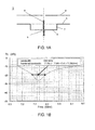
- Fig. 1A is a cross-sectional view of an antenna using a feeder circuit for a parallel-plate transmission mode
- Fig. 1B shows return loss characteristics of the antenna.
- the antenna 1 shown in Fig. 1A has an upper conductive plate 2, a lower conductive plate 3, a coaxial central conductor 4, a guide portion 5, and a short-circuit portion 7.
- the upper conductive plate 2 and the lower conductive plate 3 are provided substantially in parallel to each other.
- a central portion of the lower conductive plate 3 is recessed downward so as to form the short-circuit portion 7.
- a conductor at the bottom of the short-circuit portion 7 forms a short-circuit plate 8.
- the coaxial central conductor 4 protected by the guide portion 5 is fixed on the short-circuit plate 8 at a central portion of the antenna.
- the lower conductive plate 3, the coaxial central conductor 4, the guide portion 5, the short-circuit portion 7, and the short-circuit plate 8 of the antenna except the upper conductive plate 2 are collectively referred to as a feeder circuit.
- Fig. 1B shows the frequency dependency of return loss (RL) characteristics of this antenna.
- the return loss is defined by a ratio of an incident power to an antenna and a reflected power from the antenna. A small value of the return loss means that the antenna matches the frequency.
- the return loss is equal to or smaller than -20 dB, i.e., if the loss of power is equal to or less than 1 %, then it is determined that an antenna matches the frequency. Therefore, in the case of the antenna shown in Fig.
- the central frequency is 7.75 GHz
- the lower limit frequency is 7.4 GHz
- the upper limit frequency is 7.95 GHz.
- the bandwidth is 550 MHz
- the fractional bandwidth is 7.1 %.
- the bandwidth of this antenna is wider as compared to conventional antennas and is improved to be 550 MHz. Nevertheless, there is a demand for further increasing the bandwidth of the antenna.
- An object of the present invention is to provide technology for solving the problem that the bandwidth of an antenna and a feeder circuit should be increased and to provide a wide-band feeder circuit operable in a wide frequency band and an antenna having such a wide-band feeder circuit.
- a wide-band feeder circuit is characterized by comprising a lower conductive plate provided substantially in parallel to an upper conductive plate; a short-circuit portion provided in a concave manner at a central portion of the lower conductive plate; and a countersunk portion provided in a convex manner at a central portion of a short-circuit plate forming a bottom of the short-circuit portion.
- an antenna according to the present invention is characterized by comprising a wide-band feeder circuit including a lower conductive plate, a short-circuit portion provided in a concave manner at a central portion of the lower conductive plate, and a countersunk portion provided in a convex manner at a central portion of a short-circuit plate forming a bottom of the short-circuit portion; and an upper conductive plate provided substantially in parallel to the lower conductive plate.
- a short-circuit portion is provided in a concave manner on a lower conductive plate. Additionally, a countersunk portion is provided in a convex manner on the short-circuit portion.
- the short-circuit portion has a two-stage structure. Therefore, it is possible to increase the bandwidth of an antenna. According to the present invention, it is possible to obtain a wide-band feeder circuit having a wide bandwidth and an antenna for a parallel-plate transmission mode with such a wide-band feeder circuit.
- FIG. 2A is a cross-sectional view of an antenna using a feeder circuit for a parallel-plate transmission mode according to the first embodiment of the present invention.
- Fig. 2B shows the frequency dependency of return loss characteristics of the antenna.
- the antenna 10 shown in Fig. 2A has an upper conductive plate 2, a lower conductive plate 3, a coaxial central conductor 4, a guide portion 5, a reverse conical conductor 6, and a short-circuit portion 7.
- Each of the upper conductive plate 2 and the lower conductive plate 3 is formed of a circular conductor.
- the upper conductive plate 2 and the lower conductive plate 3 are provided substantially in parallel to each other.
- Part of a central portion of the lower conductive plate 3 is recessed downward in a circular form so as to form the short-circuit portion 7.
- the diameter of the short-circuit portion 7 is defined by A, and the depth of the short-circuit portion 7 is defined by H 1 .
- a conductive plate at the bottom of the short-circuit portion forms a short-circuit plate 8.
- the short-circuit plate 8 is substantially in parallel to the upper conductive plate 2 and the lower conductive plate 3.
- the coaxial central conductor 4 protected by the guide portion 5 is fixed on a central portion of the short-circuit plate 8.
- the reverse conical conductor 6, which has been thickened in a reverse conical form as shown in Fig. 2A is provided at a tip of the coaxial central conductor 4.
- the center of the antenna in a plan view is indicated by a chain line.
- the centers of the upper conductive plate 2, the lower conductive plate 3, and the short-circuit portion 7 are located on a straight line indicated by the chain line and are thus located substantially at the center of the antenna. Therefore, the coaxial central conductor 4 and the reverse conical conductor 6 are located at the centers of the upper conductive plate 2, the lower conductive plate 3, and the short-circuit portion 7, i.e., at the central portion of the antenna.
- the bandwidth can be increased by providing the reverse conical conductor 6 at the tip of the coaxial central conductor 4.
- the size of the reverse conical conductor 6 can be determined by the frequency to be matched.
- Fig. 2B shows the frequency dependency of return loss (RL) characteristics of the antenna with the reverse conical conductor 6.
- the central frequency is 7.75 GHz
- the lower limit frequency is 7.25 GHz
- the upper limit frequency is 7.95 GHz.
- the bandwidth is 700 MHz
- the fractional bandwidth is 9 %.
- the antenna exhibits the same central frequency of 7.75 GHz and the same upper limit frequency of 7.95 GHz as the conventional example.
- the lower limit frequency is decreased from 7.4 GHz to 7.25 GHz.
- the antenna exhibits an improved bandwidth of 700 MHz and an improved fractional bandwidth of 9 %.
- a tip of a coaxial central conductor in a feeder circuit is thickened as a reverse conical conductor. Therefore, the lower limit frequency of the antenna is decreased so as to increase the bandwidth and the fractional bandwidth.
- a wide-band feeder circuit operable in a wide frequency band and an antenna having such a wide-band feeder circuit can be obtained by thickening a tip of a coaxial central conductor as a reverse conical conductor in a feeder circuit.
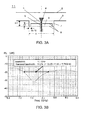
- FIG. 3A is a cross-sectional view of an antenna using a feeder circuit for a parallel-plate transmission mode according to the second embodiment of the present invention.
- Fig. 3B shows the frequency dependency of return loss characteristics of the antenna.
- a countersunk portion is further provided on the short-circuit portion of the first embodiment.
- the antenna 11 shown in Fig. 3A has an upper conductive plate 2, a lower conductive plate 3, a coaxial central conductor 4, a guide portion 5, a reverse conical conductor 6, a short-circuit portion 7, a short-circuit plate 8, and a countersunk portion 9.
- the countersunk portion 9 is added to the configuration of the first embodiment.
- the same components as in the configuration of the first embodiment are denoted by the same reference numerals, and the explanation thereof is omitted herein.
- the countersunk portion 9 is formed in a convex manner projecting toward the short-circuit portion 7 at a central portion of the short-circuit plate 8.
- the short-circuit portion 7 is formed in a concave manner projecting downward from the lower conductive plate 3.
- the countersunk portion 9 is formed in a convex manner projecting from the bottom of the short-circuit portion 7 in an upward direction, which is opposite to the direction in which the short-circuit portion 7 projects.
- the bottom of the countersunk portion 6, which is illustrated on an upper side in Fig. 3A is substantially in parallel to the upper conductive plate 2 and the lower conductive plate 3.
- Each of the countersunk portion 9 and the short-circuit portion 7 has a circular shape.
- the centers of the countersunk portion 9 and the short-circuit portion 7 are aligned with a straight line indicated by the chain line, which represents the center of the antenna.
- the diameter of the short-circuit portion 7 is defined by A, and the depth of the short-circuit portion 7 is defined by H 1.
- the countersunk portion 9 is provided inside from an edge of the short-circuit plate by B /2 .
- the diameter of the countersunk portion 9 is defined by ( A - B ), and the depth of the countersunk portion 9 is defined by H 2.
- the short-circuit portion 7 has a two-stage structure.
- a first stage is formed by a space having a diameter of A, and a second stage is formed by a space in the form of a groove formed below the first stage.
- the bandwidth of the frequency can further be increased with this two-stage structure.
- the size of the countersunk portion 9 can be determined by the frequency to be matched.
- Fig. 3B shows the frequency dependency of return loss (RL) characteristics of the antenna. Referring to Fig. 3B , the central frequency is 7.75 GHz, the lower limit frequency is 7.15 GHz, and the upper limit frequency is 8.25 GHz. Thus, the band is widened.
- the bandwidth is 1.1 GHz, and the fractional bandwidth is 14.2 %.
- the upper limit frequency is increased from 7.95 GHz to 8.25 GHz, whereas the lower limit frequency is further decreased from 7.25 GHz to 7.15 GHz.
- the antenna exhibits an improved bandwidth of 1.1 GHz and an improved fractional bandwidth of 14.2 %.
- a countersunk portion 9 is provided on a short-circuit portion 7 so that the short-circuit portion has a two-stage structure. Therefore, a difference between the upper limit frequency and the lower limit frequency of the antenna can be enlarged so as to increase the bandwidth and the fractional bandwidth of the antenna.
- a wide-band feeder circuit operable in a wide frequency band and an antenna having such a wide-band feeder circuit can be obtained by a short-circuit portion having a two-stage structure.
- FIG. 4A is a cross-sectional view of an antenna using a feeder circuit for a parallel-plate transmission mode according to the third embodiment of the present invention.
- Fig. 4B shows the frequency dependency of return loss characteristics of the antenna.
- sidewalls of the short-circuit portion and the countersunk portion of the second embodiment are tapered.
- the antenna 12 shown in Fig. 4A has an upper conductive plate 2, a lower conductive plate 3, a coaxial central conductor 4, a guide portion 5, a reverse conical conductor 6, a short-circuit portion 7, a short-circuit plate 8, and a countersunk portion 9.
- the same components as in the configuration of the second embodiment are denoted by the same reference numerals, and the explanation thereof is omitted herein.
- sidewalls of the short-circuit portion 7 and the countersunk portion 9 are tapered and inclined.
- the sidewall of the short-circuit portion 7 is inclined from the vertical state by a distance of ⁇ so as to widen a joint surface of the short-circuit portion 7 with the lower conductive plate 3 by ⁇ .
- the sidewall of the short-circuit portion 7 is inclined at ⁇ / H 1.
- the sidewall of the countersunk portion 9 is inclined from the vertical state by a distance of ⁇ so as to narrow an upper surface of the convex portion by ⁇ .
- the sidewall of the countersunk portion 9 is inclined at ⁇ / H 2.
- the inclinations of ⁇ / H 1 and ⁇ / H 2 can be determined by the frequency to be matched.
- Fig. 4B shows the frequency dependency of return loss (RL) characteristics of the antenna. Referring to Fig. 4B , the central frequency is 7.75 GHz, the lower limit frequency is 7.05 GHz, and the upper limit frequency is 8.65 GHz. The bandwidth is 1.6 GHz, and the fractional bandwidth is 20.6 %. Thus, it can be seen that the bandwidth is further increased.
- the antenna When the present embodiment is compared to the second embodiment, the upper limit frequency is increased from 8.25 GHz to 8.65 GHz, whereas the lower limit frequency is decreased from 7.15 GHz to 7.05 GHz. As a result, the antenna exhibits an improved bandwidth of 1.1 GHz and an improved fractional bandwidth of 20.6 %.
- a countersunk portion 9 is provided on a short-circuit portion 7, and sidewalls of the short-circuit portion 7 and the countersunk portion 9 are inclined. Therefore, a difference between the upper limit frequency and the lower limit frequency of the antenna can be enlarged so as to further increase the bandwidth and the fractional bandwidth of the antenna.
- a wide-band feeder circuit operable in a wide frequency band and an antenna having such a wide-band feeder circuit can be obtained by inclining sidewalls of a short-circuit portion and a countersunk portion.
- a wide-band feeder circuit according to the present invention is characterized by having a lower conductive plate provided substantially in parallel to an upper conductive plate; a short-circuit portion provided in a concave manner at a central portion of the lower conductive plate; and a countersunk portion provided in a convex manner at a central portion of a short-circuit plate forming a bottom of the short-circuit portion.
- a sidewall of the short-circuit portion of the wide-band feeder circuit may be inclined.
- a sidewall of the countersunk portion may also be inclined.
- Each of the short-circuit portion and the countersunk portion may have a circular shape. The centers of the short-circuit portion and the countersunk portion may be aligned with the same straight line.
- the wide-band feeder circuit may have a coaxial central conductor protected at the center of the countersunk portion by a guide portion, and a reverse conical conductor may be formed at a tip of the coaxial central conductor.
- an antenna including the aforementioned wide-band feeder circuit can be used for a parallel-plate transmission mode.
Landscapes
- Waveguide Aerials (AREA)
- Details Of Aerials (AREA)
Abstract
Description
- The present invention relates to an antenna, and more particularly to a wide-band feeder circuit operable in a wide frequency band and an antenna having such a wide-band feeder circuit.
- Various antennas have been used for mobile communication such as satellite communication, a global positioning system (GPS), and cellular phones. Thus, antennas are used for various purposes. Therefore, an increase of the bandwidth is required such that an antenna operates in a wide frequency band. Heretofore, antennas using a device that does not have a very wide band, such as slot antennas, have mainly been used for a parallel-plate transmission mode. However, various applications of a device having a wide band, such as a helical antenna, have been developed recently. Accordingly, a feeder circuit is also required to have a widened band.
- There is an antenna developed by the inventors in order to widen the band of an antenna and a feeder circuit.
Fig. 1A is a cross-sectional view of an antenna using a feeder circuit for a parallel-plate transmission mode, andFig. 1B shows return loss characteristics of the antenna. Theantenna 1 shown inFig. 1A has an upperconductive plate 2, a lowerconductive plate 3, a coaxialcentral conductor 4, aguide portion 5, and a short-circuit portion 7. The upperconductive plate 2 and the lowerconductive plate 3 are provided substantially in parallel to each other. A central portion of the lowerconductive plate 3 is recessed downward so as to form the short-circuit portion 7. A conductor at the bottom of the short-circuit portion 7 forms a short-circuit plate 8. The coaxialcentral conductor 4 protected by theguide portion 5 is fixed on the short-circuit plate 8 at a central portion of the antenna. In the present invention, the lowerconductive plate 3, the coaxialcentral conductor 4, theguide portion 5, the short-circuit portion 7, and the short-circuit plate 8 of the antenna except the upperconductive plate 2 are collectively referred to as a feeder circuit. - In this antenna, the short-
circuit portion 7, which is recessed downward at the central portion of the lowerconductive plate 3, serves as an impedance conversion circuit, thereby increasing the bandwidth of frequencies.Fig. 1B shows the frequency dependency of return loss (RL) characteristics of this antenna. The return loss is defined by a ratio of an incident power to an antenna and a reflected power from the antenna. A small value of the return loss means that the antenna matches the frequency. In the present invention, if the return loss is equal to or smaller than -20 dB, i.e., if the loss of power is equal to or less than 1 %, then it is determined that an antenna matches the frequency. Therefore, in the case of the antenna shown inFig. 1 , the central frequency is 7.75 GHz, the lower limit frequency is 7.4 GHz, and the upper limit frequency is 7.95 GHz. The bandwidth is 550 MHz, and the fractional bandwidth is 7.1 %. The bandwidth of this antenna is wider as compared to conventional antennas and is improved to be 550 MHz. Nevertheless, there is a demand for further increasing the bandwidth of the antenna. - As described above, an increase of the bandwidth of an antenna and a feeder circuit has increasingly been demanded. Thus, there is a problem that a further increase of the bandwidth has been desired.
- An object of the present invention is to provide technology for solving the problem that the bandwidth of an antenna and a feeder circuit should be increased and to provide a wide-band feeder circuit operable in a wide frequency band and an antenna having such a wide-band feeder circuit.
- A wide-band feeder circuit according to the present invention is characterized by comprising a lower conductive plate provided substantially in parallel to an upper conductive plate; a short-circuit portion provided in a concave manner at a central portion of the lower conductive plate; and a countersunk portion provided in a convex manner at a central portion of a short-circuit plate forming a bottom of the short-circuit portion. Furthermore, an antenna according to the present invention is characterized by comprising a wide-band feeder circuit including a lower conductive plate, a short-circuit portion provided in a concave manner at a central portion of the lower conductive plate, and a countersunk portion provided in a convex manner at a central portion of a short-circuit plate forming a bottom of the short-circuit portion; and an upper conductive plate provided substantially in parallel to the lower conductive plate.
- According to the present invention, a short-circuit portion is provided in a concave manner on a lower conductive plate. Additionally, a countersunk portion is provided in a convex manner on the short-circuit portion. Thus, the short-circuit portion has a two-stage structure. Therefore, it is possible to increase the bandwidth of an antenna. According to the present invention, it is possible to obtain a wide-band feeder circuit having a wide bandwidth and an antenna for a parallel-plate transmission mode with such a wide-band feeder circuit.
- Brief Description of Drawings:
-
Fig. 1A is a cross-sectional view of a conventional antenna. -
Fig. 1B is a graph showing frequency dependency of return loss characteristics of the antenna shown inFig. 1A . -
Fig. 2A is a cross-sectional view of an antenna according to a first embodiment of the present invention. -
Fig. 2B is a graph showing frequency dependency of return loss characteristics of the antenna shown inFig. 2A . -
Fig. 3A is a cross-sectional view of an antenna according to a second embodiment of the present invention. -
Fig. 3B is a graph showing frequency dependency of return loss characteristics of the antenna shown inFig. 3A . -
Fig. 4A is a cross-sectional view of an antenna according to a third embodiment of the present invention. -
Fig. 4B is a graph showing frequency dependency of return loss characteristics of the antenna shown inFig. 4A . - Embodiments of the present invention will be described in detail with reference to the drawings.
- A first embodiment of the present invention will be described in detail with reference to
Figs. 2A and 2B. Fig. 2A is a cross-sectional view of an antenna using a feeder circuit for a parallel-plate transmission mode according to the first embodiment of the present invention.Fig. 2B shows the frequency dependency of return loss characteristics of the antenna. - The
antenna 10 shown inFig. 2A has an upperconductive plate 2, a lowerconductive plate 3, a coaxialcentral conductor 4, aguide portion 5, a reverseconical conductor 6, and a short-circuit portion 7. Each of the upperconductive plate 2 and the lowerconductive plate 3 is formed of a circular conductor. The upperconductive plate 2 and the lowerconductive plate 3 are provided substantially in parallel to each other. Part of a central portion of the lowerconductive plate 3 is recessed downward in a circular form so as to form the short-circuit portion 7. The diameter of the short-circuit portion 7 is defined by A, and the depth of the short-circuit portion 7 is defined by H1 . A conductive plate at the bottom of the short-circuit portion forms a short-circuit plate 8. The short-circuit plate 8 is substantially in parallel to the upperconductive plate 2 and the lowerconductive plate 3. The coaxialcentral conductor 4 protected by theguide portion 5 is fixed on a central portion of the short-circuit plate 8. Furthermore, the reverseconical conductor 6, which has been thickened in a reverse conical form as shown inFig. 2A , is provided at a tip of the coaxialcentral conductor 4. The center of the antenna in a plan view is indicated by a chain line. The centers of the upperconductive plate 2, the lowerconductive plate 3, and the short-circuit portion 7 are located on a straight line indicated by the chain line and are thus located substantially at the center of the antenna. Therefore, the coaxialcentral conductor 4 and the reverseconical conductor 6 are located at the centers of the upperconductive plate 2, the lowerconductive plate 3, and the short-circuit portion 7, i.e., at the central portion of the antenna. - The bandwidth can be increased by providing the reverse
conical conductor 6 at the tip of the coaxialcentral conductor 4. The size of the reverseconical conductor 6 can be determined by the frequency to be matched.Fig. 2B shows the frequency dependency of return loss (RL) characteristics of the antenna with the reverseconical conductor 6. Referring toFig. 2B , the central frequency is 7.75 GHz, the lower limit frequency is 7.25 GHz, and the upper limit frequency is 7.95 GHz. The bandwidth is 700 MHz, and the fractional bandwidth is 9 %. Thus, it can be seen that the bandwidth is increased. The antenna exhibits the same central frequency of 7.75 GHz and the same upper limit frequency of 7.95 GHz as the conventional example. However, the lower limit frequency is decreased from 7.4 GHz to 7.25 GHz. As a result, the antenna exhibits an improved bandwidth of 700 MHz and an improved fractional bandwidth of 9 %. - According to the present embodiment, a tip of a coaxial central conductor in a feeder circuit is thickened as a reverse conical conductor. Therefore, the lower limit frequency of the antenna is decreased so as to increase the bandwidth and the fractional bandwidth. Thus, a wide-band feeder circuit operable in a wide frequency band and an antenna having such a wide-band feeder circuit can be obtained by thickening a tip of a coaxial central conductor as a reverse conical conductor in a feeder circuit.
- A second embodiment of the present invention will be described in detail with reference to
Figs. 3A and 3B. Fig. 3A is a cross-sectional view of an antenna using a feeder circuit for a parallel-plate transmission mode according to the second embodiment of the present invention.Fig. 3B shows the frequency dependency of return loss characteristics of the antenna. In the second embodiment, a countersunk portion is further provided on the short-circuit portion of the first embodiment. - The
antenna 11 shown inFig. 3A has an upperconductive plate 2, a lowerconductive plate 3, a coaxialcentral conductor 4, aguide portion 5, a reverseconical conductor 6, a short-circuit portion 7, a short-circuit plate 8, and acountersunk portion 9. In the configuration of the second embodiment, the countersunkportion 9 is added to the configuration of the first embodiment. The same components as in the configuration of the first embodiment are denoted by the same reference numerals, and the explanation thereof is omitted herein. The countersunkportion 9 is formed in a convex manner projecting toward the short-circuit portion 7 at a central portion of the short-circuit plate 8. The short-circuit portion 7 is formed in a concave manner projecting downward from the lowerconductive plate 3. The countersunkportion 9 is formed in a convex manner projecting from the bottom of the short-circuit portion 7 in an upward direction, which is opposite to the direction in which the short-circuit portion 7 projects. The bottom of the countersunkportion 6, which is illustrated on an upper side inFig. 3A , is substantially in parallel to the upperconductive plate 2 and the lowerconductive plate 3. - Each of the countersunk
portion 9 and the short-circuit portion 7 has a circular shape. The centers of the countersunkportion 9 and the short-circuit portion 7 are aligned with a straight line indicated by the chain line, which represents the center of the antenna. The diameter of the short-circuit portion 7 is defined by A, and the depth of the short-circuit portion 7 is defined by H1. The countersunkportion 9 is provided inside from an edge of the short-circuit plate by B/2. The diameter of the countersunkportion 9 is defined by (A - B), and the depth of the countersunkportion 9 is defined by H2. - With the countersunk
portion 9 provided on the short-circuit portion 7, the short-circuit portion 7 has a two-stage structure. A first stage is formed by a space having a diameter of A, and a second stage is formed by a space in the form of a groove formed below the first stage. The bandwidth of the frequency can further be increased with this two-stage structure. The size of the countersunkportion 9 can be determined by the frequency to be matched.Fig. 3B shows the frequency dependency of return loss (RL) characteristics of the antenna. Referring toFig. 3B , the central frequency is 7.75 GHz, the lower limit frequency is 7.15 GHz, and the upper limit frequency is 8.25 GHz. Thus, the band is widened. The bandwidth is 1.1 GHz, and the fractional bandwidth is 14.2 %. When the present embodiment is compared to the first embodiment, the upper limit frequency is increased from 7.95 GHz to 8.25 GHz, whereas the lower limit frequency is further decreased from 7.25 GHz to 7.15 GHz. As a result, the antenna exhibits an improved bandwidth of 1.1 GHz and an improved fractional bandwidth of 14.2 %. - According to the present embodiment, a countersunk
portion 9 is provided on a short-circuit portion 7 so that the short-circuit portion has a two-stage structure. Therefore, a difference between the upper limit frequency and the lower limit frequency of the antenna can be enlarged so as to increase the bandwidth and the fractional bandwidth of the antenna. Thus, a wide-band feeder circuit operable in a wide frequency band and an antenna having such a wide-band feeder circuit can be obtained by a short-circuit portion having a two-stage structure. - A third embodiment of the present invention will be described in detail with reference to
Fig. 4A and 4B. Fig. 4A is a cross-sectional view of an antenna using a feeder circuit for a parallel-plate transmission mode according to the third embodiment of the present invention.Fig. 4B shows the frequency dependency of return loss characteristics of the antenna. In the third embodiment, sidewalls of the short-circuit portion and the countersunk portion of the second embodiment are tapered. - The
antenna 12 shown inFig. 4A has an upperconductive plate 2, a lowerconductive plate 3, a coaxialcentral conductor 4, aguide portion 5, a reverseconical conductor 6, a short-circuit portion 7, a short-circuit plate 8, and acountersunk portion 9. The same components as in the configuration of the second embodiment are denoted by the same reference numerals, and the explanation thereof is omitted herein. In the present embodiment, sidewalls of the short-circuit portion 7 and the countersunkportion 9 are tapered and inclined. The sidewall of the short-circuit portion 7 is inclined from the vertical state by a distance of β so as to widen a joint surface of the short-circuit portion 7 with the lowerconductive plate 3 by β. - Thus, the sidewall of the short-
circuit portion 7 is inclined at β/H1. The sidewall of the countersunkportion 9 is inclined from the vertical state by a distance of α so as to narrow an upper surface of the convex portion by α. Thus, the sidewall of the countersunkportion 9 is inclined at α/H2. In this manner, the sidewalls of the short-circuit portion 7 and the countersunkportion 9 are tapered and inclined. The inclinations of β/H1 and α/H2 can be determined by the frequency to be matched. - When the sidewalls of the short-
circuit portion 7 and the countersunkportion 9 are tapered and inclined, the bandwidth of the frequency can further be increased. With the inclined sidewalls, the short-circuit locations and the short-circuit radius are made ambiguous, so that the bandwidth is further increased.Fig. 4B shows the frequency dependency of return loss (RL) characteristics of the antenna. Referring toFig. 4B , the central frequency is 7.75 GHz, the lower limit frequency is 7.05 GHz, and the upper limit frequency is 8.65 GHz. The bandwidth is 1.6 GHz, and the fractional bandwidth is 20.6 %. Thus, it can be seen that the bandwidth is further increased. When the present embodiment is compared to the second embodiment, the upper limit frequency is increased from 8.25 GHz to 8.65 GHz, whereas the lower limit frequency is decreased from 7.15 GHz to 7.05 GHz. As a result, the antenna exhibits an improved bandwidth of 1.1 GHz and an improved fractional bandwidth of 20.6 %. - According to the present embodiment, a countersunk
portion 9 is provided on a short-circuit portion 7, and sidewalls of the short-circuit portion 7 and the countersunkportion 9 are inclined. Therefore, a difference between the upper limit frequency and the lower limit frequency of the antenna can be enlarged so as to further increase the bandwidth and the fractional bandwidth of the antenna. Thus, a wide-band feeder circuit operable in a wide frequency band and an antenna having such a wide-band feeder circuit can be obtained by inclining sidewalls of a short-circuit portion and a countersunk portion. - The present invention has been described with some embodiments. A wide-band feeder circuit according to the present invention is characterized by having a lower conductive plate provided substantially in parallel to an upper conductive plate; a short-circuit portion provided in a concave manner at a central portion of the lower conductive plate; and a countersunk portion provided in a convex manner at a central portion of a short-circuit plate forming a bottom of the short-circuit portion.
- Furthermore, a sidewall of the short-circuit portion of the wide-band feeder circuit may be inclined. Moreover, a sidewall of the countersunk portion may also be inclined. Each of the short-circuit portion and the countersunk portion may have a circular shape. The centers of the short-circuit portion and the countersunk portion may be aligned with the same straight line. Furthermore, the wide-band feeder circuit may have a coaxial central conductor protected at the center of the countersunk portion by a guide portion, and a reverse conical conductor may be formed at a tip of the coaxial central conductor.
- Moreover, according to the present invention, it is possible to obtain an antenna including the aforementioned wide-band feeder circuit. This antenna can be used for a parallel-plate transmission mode.
- While the present invention has been described with reference to the embodiments, the present invention is not limited to the aforementioned embodiments. It would be apparent to those skillet in the art that various changes may be made in configuration and details of the present invention without departing from the scope of the present invention.
- This application claims the benefit of priority from Japanese patent application No.
2008-071200, filed on March 19, 2008
Claims (12)
- A wide-band feeder circuit characterized by comprising:a lower conductive plate provided substantially in parallel to an upper conductive plate; a short-circuit portion provided in a concave manner at a central portion of the lower conductive plate; and a countersunk portion provided in a convex manner at a central portion of a short-circuit plate forming a bottom of the short-circuit portion.
- The wide-band feeder circuit as recited in claim 1, characterized in that a sidewall of the short-circuit portion is inclined.
- The wide-band feeder circuit as recited in claim 1 or 2, characterized in that a sidewall of the countersunk portion is inclined.
- The wide-band feeder circuit as recited in claim 3, characterized in that each of the short-circuit portion and the countersunk portion has a circular shape, and centers of the short-circuit portion and the countersunk portion are aligned with the same straight line.
- The wide-band feeder circuit as recited in claim 4, characterized by comprising a coaxial central conductor protected at the center of the countersunk portion by a guide portion.
- The wide-band feeder circuit as recited in claim 5, characterized in that a reverse conical conductor is formed at a tip of the coaxial central conductor.
- An antenna characterized by comprising:a wide-band feeder circuit including a lower conductive plate, a short-circuit portion provided in a concave manner at a central portion of the lower conductive plate, and a countersunk portion provided in a convex manner at a central portion of a short-circuit plate forming a bottom of the short-circuit portion; and an upper conductive plate provided substantially in parallel to the lower conductive plate.
- The antenna as recited in claim 7, characterized in that a sidewall of the short-circuit portion is inclined.
- The antenna as recited in claim 7 or 8, characterized in that a sidewall of the countersunk portion is inclined.
- The antenna as recited in claim 9, characterized in that each of the short-circuit portion and the countersunk portion has a circular shape, and centers of the short-circuit portion and the countersunk portion are aligned with the same straight line.
- The antenna as recited in claim 10, characterized by comprising a coaxial central conductor protected at the center of the countersunk portion by a guide portion.
- The antenna as recited in claim 11, characterized in that a reverse conical conductor is formed at a tip of the coaxial central conductor.
Applications Claiming Priority (2)
| Application Number | Priority Date | Filing Date | Title |
|---|---|---|---|
| JP2008071200A JP5299749B2 (en) | 2008-03-19 | 2008-03-19 | Broadband power feeding circuit and slot antenna having the same |
| PCT/JP2009/056027 WO2009116686A1 (en) | 2008-03-19 | 2009-03-18 | Broadband power supply circuit and antenna equipped with the same |
Publications (3)
| Publication Number | Publication Date |
|---|---|
| EP2256865A1 true EP2256865A1 (en) | 2010-12-01 |
| EP2256865A4 EP2256865A4 (en) | 2014-03-26 |
| EP2256865B1 EP2256865B1 (en) | 2015-12-16 |
Family
ID=41091076
Family Applications (1)
| Application Number | Title | Priority Date | Filing Date |
|---|---|---|---|
| EP09721870.5A Active EP2256865B1 (en) | 2008-03-19 | 2009-03-18 | Wide-band feder circuit and antenna having the same |
Country Status (5)
| Country | Link |
|---|---|
| US (1) | US9048534B2 (en) |
| EP (1) | EP2256865B1 (en) |
| JP (1) | JP5299749B2 (en) |
| CN (1) | CN101978555B (en) |
| WO (1) | WO2009116686A1 (en) |
Families Citing this family (1)
| Publication number | Priority date | Publication date | Assignee | Title |
|---|---|---|---|---|
| CN103490167A (en) * | 2013-08-14 | 2014-01-01 | 京信通信技术(广州)有限公司 | High-gain smoothing antenna |
Family Cites Families (10)
| Publication number | Priority date | Publication date | Assignee | Title |
|---|---|---|---|---|
| JP2817363B2 (en) * | 1990-06-25 | 1998-10-30 | 凸版印刷株式会社 | Power supply device |
| JPH0485905A (en) | 1990-07-30 | 1992-03-18 | Matsushita Electric Ind Co Ltd | Rotary transformer |
| JPH0485905U (en) * | 1990-11-30 | 1992-07-27 | ||
| JP3259098B2 (en) * | 1991-09-30 | 2002-02-18 | 有限会社中村製作所 | Linear polarized antenna device |
| JPH06244634A (en) * | 1993-02-12 | 1994-09-02 | Naohisa Goto | Feeding circuit for planar antenna |
| JP2840562B2 (en) | 1995-01-17 | 1998-12-24 | キヤノン株式会社 | Camera having focus detection device |
| US8273605B2 (en) * | 2003-12-05 | 2012-09-25 | Hitachi Chemical Co., Ltd. | Manufacturing method for electronic device having IC chip and antenna electrically connected by bridging plate |
| JP2006074328A (en) | 2004-09-01 | 2006-03-16 | Tokyo Keiso Co Ltd | TE01 mode microwave exciter for circular waveguide |
| EP1796207A4 (en) * | 2004-09-28 | 2009-06-17 | Panasonic Corp | RADIO ANTENNA DEVICE AND PORTABLE RADIO |
| JP2006210402A (en) * | 2005-01-25 | 2006-08-10 | Matsushita Electric Ind Co Ltd | Semiconductor device |
-
2008
- 2008-03-19 JP JP2008071200A patent/JP5299749B2/en active Active
-
2009
- 2009-03-18 CN CN200980109793.8A patent/CN101978555B/en active Active
- 2009-03-18 US US12/922,743 patent/US9048534B2/en not_active Expired - Fee Related
- 2009-03-18 EP EP09721870.5A patent/EP2256865B1/en active Active
- 2009-03-18 WO PCT/JP2009/056027 patent/WO2009116686A1/en not_active Ceased
Also Published As
| Publication number | Publication date |
|---|---|
| EP2256865B1 (en) | 2015-12-16 |
| US9048534B2 (en) | 2015-06-02 |
| JP5299749B2 (en) | 2013-09-25 |
| CN101978555B (en) | 2014-12-24 |
| US20110006970A1 (en) | 2011-01-13 |
| CN101978555A (en) | 2011-02-16 |
| WO2009116686A1 (en) | 2009-09-24 |
| EP2256865A4 (en) | 2014-03-26 |
| JP2009231875A (en) | 2009-10-08 |
Similar Documents
| Publication | Publication Date | Title |
|---|---|---|
| US9673531B2 (en) | Antenna | |
| US8736494B2 (en) | Dual band antenna | |
| US8593354B2 (en) | Multi-band antenna | |
| US20120287009A1 (en) | Solid antenna | |
| CN101562277B (en) | Printed antenna | |
| US20220344834A1 (en) | Flexible polymer antenna with multiple ground resonators | |
| US9728846B2 (en) | Low passive intermodulation antenna apparatus and methods of use | |
| US20170331194A1 (en) | Communication device | |
| US20090315785A1 (en) | Antenna and wireless communication device using same | |
| US10587051B2 (en) | Communication device | |
| US11784400B2 (en) | Thin antenna | |
| EP2256865B1 (en) | Wide-band feder circuit and antenna having the same | |
| US8963779B2 (en) | Silicon-based suspending antenna with photonic bandgap structure | |
| US8085205B2 (en) | Antenna module and an electronic device having the antenna module | |
| US20090128420A1 (en) | Dual band antenna | |
| US7382326B1 (en) | Multi-band antenna | |
| CN103647145A (en) | Broadband modularized antenna and antenna assembly with same | |
| CN211957926U (en) | Three-in-one antenna | |
| US8339319B2 (en) | Broadband antenna | |
| KR101218718B1 (en) | Diversity antenna device and mobile using the same | |
| US20150364825A1 (en) | Dual-band three-dimensional antenna | |
| US20110148735A1 (en) | Dual-band antenna | |
| JP6362352B2 (en) | Planar broadband antenna | |
| EP3065216A1 (en) | Monopole antenna | |
| JP4935256B2 (en) | Antenna device |
Legal Events
| Date | Code | Title | Description |
|---|---|---|---|
| PUAI | Public reference made under article 153(3) epc to a published international application that has entered the european phase |
Free format text: ORIGINAL CODE: 0009012 |
|
| 17P | Request for examination filed |
Effective date: 20100916 |
|
| AK | Designated contracting states |
Kind code of ref document: A1 Designated state(s): AT BE BG CH CY CZ DE DK EE ES FI FR GB GR HR HU IE IS IT LI LT LU LV MC MK MT NL NO PL PT RO SE SI SK TR |
|
| AX | Request for extension of the european patent |
Extension state: AL BA RS |
|
| DAX | Request for extension of the european patent (deleted) | ||
| A4 | Supplementary search report drawn up and despatched |
Effective date: 20140226 |
|
| RIC1 | Information provided on ipc code assigned before grant |
Ipc: H01Q 13/18 20060101ALI20140220BHEP Ipc: H01Q 13/22 20060101AFI20140220BHEP Ipc: H01Q 1/24 20060101ALI20140220BHEP |
|
| GRAP | Despatch of communication of intention to grant a patent |
Free format text: ORIGINAL CODE: EPIDOSNIGR1 |
|
| RIC1 | Information provided on ipc code assigned before grant |
Ipc: H01Q 1/24 20060101ALI20150414BHEP Ipc: H01Q 13/18 20060101ALI20150414BHEP Ipc: H01Q 13/22 20060101AFI20150414BHEP |
|
| INTG | Intention to grant announced |
Effective date: 20150511 |
|
| RIN1 | Information on inventor provided before grant (corrected) |
Inventor name: KAMATA, YUKIO Inventor name: AMANO, OSAMU Inventor name: ANDO, MAKOTO Inventor name: KOREEDA, SHUICHI |
|
| GRAS | Grant fee paid |
Free format text: ORIGINAL CODE: EPIDOSNIGR3 |
|
| RIN1 | Information on inventor provided before grant (corrected) |
Inventor name: AMANO, OSAMU Inventor name: ANDO, MAKOTO Inventor name: KAMATA, YUKIO Inventor name: KOREEDA, SHUICHI |
|
| RAP1 | Party data changed (applicant data changed or rights of an application transferred) |
Owner name: JAPAN AEROSPACE EXPLORATION AGENCY Owner name: NEC SPACE TECHNOLOGIES, LTD. |
|
| GRAA | (expected) grant |
Free format text: ORIGINAL CODE: 0009210 |
|
| AK | Designated contracting states |
Kind code of ref document: B1 Designated state(s): AT BE BG CH CY CZ DE DK EE ES FI FR GB GR HR HU IE IS IT LI LT LU LV MC MK MT NL NO PL PT RO SE SI SK TR |
|
| REG | Reference to a national code |
Ref country code: GB Ref legal event code: FG4D |
|
| REG | Reference to a national code |
Ref country code: CH Ref legal event code: EP |
|
| REG | Reference to a national code |
Ref country code: IE Ref legal event code: FG4D |
|
| REG | Reference to a national code |
Ref country code: AT Ref legal event code: REF Ref document number: 765957 Country of ref document: AT Kind code of ref document: T Effective date: 20160115 |
|
| REG | Reference to a national code |
Ref country code: DE Ref legal event code: R096 Ref document number: 602009035242 Country of ref document: DE |
|
| REG | Reference to a national code |
Ref country code: FR Ref legal event code: PLFP Year of fee payment: 8 |
|
| REG | Reference to a national code |
Ref country code: NL Ref legal event code: MP Effective date: 20151216 |
|
| REG | Reference to a national code |
Ref country code: LT Ref legal event code: MG4D |
|
| PG25 | Lapsed in a contracting state [announced via postgrant information from national office to epo] |
Ref country code: HR Free format text: LAPSE BECAUSE OF FAILURE TO SUBMIT A TRANSLATION OF THE DESCRIPTION OR TO PAY THE FEE WITHIN THE PRESCRIBED TIME-LIMIT Effective date: 20151216 Ref country code: NO Free format text: LAPSE BECAUSE OF FAILURE TO SUBMIT A TRANSLATION OF THE DESCRIPTION OR TO PAY THE FEE WITHIN THE PRESCRIBED TIME-LIMIT Effective date: 20160316 Ref country code: LT Free format text: LAPSE BECAUSE OF FAILURE TO SUBMIT A TRANSLATION OF THE DESCRIPTION OR TO PAY THE FEE WITHIN THE PRESCRIBED TIME-LIMIT Effective date: 20151216 |
|
| REG | Reference to a national code |
Ref country code: AT Ref legal event code: MK05 Ref document number: 765957 Country of ref document: AT Kind code of ref document: T Effective date: 20151216 |
|
| PG25 | Lapsed in a contracting state [announced via postgrant information from national office to epo] |
Ref country code: LV Free format text: LAPSE BECAUSE OF FAILURE TO SUBMIT A TRANSLATION OF THE DESCRIPTION OR TO PAY THE FEE WITHIN THE PRESCRIBED TIME-LIMIT Effective date: 20151216 Ref country code: SE Free format text: LAPSE BECAUSE OF FAILURE TO SUBMIT A TRANSLATION OF THE DESCRIPTION OR TO PAY THE FEE WITHIN THE PRESCRIBED TIME-LIMIT Effective date: 20151216 Ref country code: GR Free format text: LAPSE BECAUSE OF FAILURE TO SUBMIT A TRANSLATION OF THE DESCRIPTION OR TO PAY THE FEE WITHIN THE PRESCRIBED TIME-LIMIT Effective date: 20160317 Ref country code: FI Free format text: LAPSE BECAUSE OF FAILURE TO SUBMIT A TRANSLATION OF THE DESCRIPTION OR TO PAY THE FEE WITHIN THE PRESCRIBED TIME-LIMIT Effective date: 20151216 Ref country code: NL Free format text: LAPSE BECAUSE OF FAILURE TO SUBMIT A TRANSLATION OF THE DESCRIPTION OR TO PAY THE FEE WITHIN THE PRESCRIBED TIME-LIMIT Effective date: 20151216 |
|
| PG25 | Lapsed in a contracting state [announced via postgrant information from national office to epo] |
Ref country code: ES Free format text: LAPSE BECAUSE OF FAILURE TO SUBMIT A TRANSLATION OF THE DESCRIPTION OR TO PAY THE FEE WITHIN THE PRESCRIBED TIME-LIMIT Effective date: 20151216 Ref country code: CZ Free format text: LAPSE BECAUSE OF FAILURE TO SUBMIT A TRANSLATION OF THE DESCRIPTION OR TO PAY THE FEE WITHIN THE PRESCRIBED TIME-LIMIT Effective date: 20151216 |
|
| PG25 | Lapsed in a contracting state [announced via postgrant information from national office to epo] |
Ref country code: SK Free format text: LAPSE BECAUSE OF FAILURE TO SUBMIT A TRANSLATION OF THE DESCRIPTION OR TO PAY THE FEE WITHIN THE PRESCRIBED TIME-LIMIT Effective date: 20151216 Ref country code: PT Free format text: LAPSE BECAUSE OF FAILURE TO SUBMIT A TRANSLATION OF THE DESCRIPTION OR TO PAY THE FEE WITHIN THE PRESCRIBED TIME-LIMIT Effective date: 20160418 Ref country code: RO Free format text: LAPSE BECAUSE OF FAILURE TO SUBMIT A TRANSLATION OF THE DESCRIPTION OR TO PAY THE FEE WITHIN THE PRESCRIBED TIME-LIMIT Effective date: 20151216 Ref country code: EE Free format text: LAPSE BECAUSE OF FAILURE TO SUBMIT A TRANSLATION OF THE DESCRIPTION OR TO PAY THE FEE WITHIN THE PRESCRIBED TIME-LIMIT Effective date: 20151216 Ref country code: BE Free format text: LAPSE BECAUSE OF NON-PAYMENT OF DUE FEES Effective date: 20160331 Ref country code: IS Free format text: LAPSE BECAUSE OF FAILURE TO SUBMIT A TRANSLATION OF THE DESCRIPTION OR TO PAY THE FEE WITHIN THE PRESCRIBED TIME-LIMIT Effective date: 20160416 Ref country code: AT Free format text: LAPSE BECAUSE OF FAILURE TO SUBMIT A TRANSLATION OF THE DESCRIPTION OR TO PAY THE FEE WITHIN THE PRESCRIBED TIME-LIMIT Effective date: 20151216 |
|
| REG | Reference to a national code |
Ref country code: DE Ref legal event code: R097 Ref document number: 602009035242 Country of ref document: DE |
|
| PLBE | No opposition filed within time limit |
Free format text: ORIGINAL CODE: 0009261 |
|
| STAA | Information on the status of an ep patent application or granted ep patent |
Free format text: STATUS: NO OPPOSITION FILED WITHIN TIME LIMIT |
|
| PG25 | Lapsed in a contracting state [announced via postgrant information from national office to epo] |
Ref country code: LU Free format text: LAPSE BECAUSE OF FAILURE TO SUBMIT A TRANSLATION OF THE DESCRIPTION OR TO PAY THE FEE WITHIN THE PRESCRIBED TIME-LIMIT Effective date: 20160318 Ref country code: PL Free format text: LAPSE BECAUSE OF FAILURE TO SUBMIT A TRANSLATION OF THE DESCRIPTION OR TO PAY THE FEE WITHIN THE PRESCRIBED TIME-LIMIT Effective date: 20151216 Ref country code: MC Free format text: LAPSE BECAUSE OF FAILURE TO SUBMIT A TRANSLATION OF THE DESCRIPTION OR TO PAY THE FEE WITHIN THE PRESCRIBED TIME-LIMIT Effective date: 20151216 Ref country code: DK Free format text: LAPSE BECAUSE OF FAILURE TO SUBMIT A TRANSLATION OF THE DESCRIPTION OR TO PAY THE FEE WITHIN THE PRESCRIBED TIME-LIMIT Effective date: 20151216 |
|
| REG | Reference to a national code |
Ref country code: CH Ref legal event code: PL |
|
| 26N | No opposition filed |
Effective date: 20160919 |
|
| REG | Reference to a national code |
Ref country code: IE Ref legal event code: MM4A |
|
| PG25 | Lapsed in a contracting state [announced via postgrant information from national office to epo] |
Ref country code: BE Free format text: LAPSE BECAUSE OF FAILURE TO SUBMIT A TRANSLATION OF THE DESCRIPTION OR TO PAY THE FEE WITHIN THE PRESCRIBED TIME-LIMIT Effective date: 20151216 |
|
| PG25 | Lapsed in a contracting state [announced via postgrant information from national office to epo] |
Ref country code: IE Free format text: LAPSE BECAUSE OF NON-PAYMENT OF DUE FEES Effective date: 20160318 Ref country code: LI Free format text: LAPSE BECAUSE OF NON-PAYMENT OF DUE FEES Effective date: 20160331 Ref country code: CH Free format text: LAPSE BECAUSE OF NON-PAYMENT OF DUE FEES Effective date: 20160331 |
|
| REG | Reference to a national code |
Ref country code: FR Ref legal event code: PLFP Year of fee payment: 9 |
|
| PG25 | Lapsed in a contracting state [announced via postgrant information from national office to epo] |
Ref country code: SI Free format text: LAPSE BECAUSE OF FAILURE TO SUBMIT A TRANSLATION OF THE DESCRIPTION OR TO PAY THE FEE WITHIN THE PRESCRIBED TIME-LIMIT Effective date: 20151216 |
|
| PG25 | Lapsed in a contracting state [announced via postgrant information from national office to epo] |
Ref country code: MT Free format text: LAPSE BECAUSE OF FAILURE TO SUBMIT A TRANSLATION OF THE DESCRIPTION OR TO PAY THE FEE WITHIN THE PRESCRIBED TIME-LIMIT Effective date: 20151216 |
|
| REG | Reference to a national code |
Ref country code: FR Ref legal event code: PLFP Year of fee payment: 10 |
|
| PG25 | Lapsed in a contracting state [announced via postgrant information from national office to epo] |
Ref country code: CY Free format text: LAPSE BECAUSE OF FAILURE TO SUBMIT A TRANSLATION OF THE DESCRIPTION OR TO PAY THE FEE WITHIN THE PRESCRIBED TIME-LIMIT Effective date: 20151216 Ref country code: HU Free format text: LAPSE BECAUSE OF FAILURE TO SUBMIT A TRANSLATION OF THE DESCRIPTION OR TO PAY THE FEE WITHIN THE PRESCRIBED TIME-LIMIT; INVALID AB INITIO Effective date: 20090318 |
|
| PG25 | Lapsed in a contracting state [announced via postgrant information from national office to epo] |
Ref country code: TR Free format text: LAPSE BECAUSE OF FAILURE TO SUBMIT A TRANSLATION OF THE DESCRIPTION OR TO PAY THE FEE WITHIN THE PRESCRIBED TIME-LIMIT Effective date: 20151216 Ref country code: MT Free format text: LAPSE BECAUSE OF FAILURE TO SUBMIT A TRANSLATION OF THE DESCRIPTION OR TO PAY THE FEE WITHIN THE PRESCRIBED TIME-LIMIT Effective date: 20160331 Ref country code: MK Free format text: LAPSE BECAUSE OF FAILURE TO SUBMIT A TRANSLATION OF THE DESCRIPTION OR TO PAY THE FEE WITHIN THE PRESCRIBED TIME-LIMIT Effective date: 20151216 |
|
| PG25 | Lapsed in a contracting state [announced via postgrant information from national office to epo] |
Ref country code: BG Free format text: LAPSE BECAUSE OF FAILURE TO SUBMIT A TRANSLATION OF THE DESCRIPTION OR TO PAY THE FEE WITHIN THE PRESCRIBED TIME-LIMIT Effective date: 20151216 |
|
| REG | Reference to a national code |
Ref country code: DE Ref legal event code: R082 Ref document number: 602009035242 Country of ref document: DE Representative=s name: VOSSIUS & PARTNER PATENTANWAELTE RECHTSANWAELT, DE Ref country code: DE Ref legal event code: R081 Ref document number: 602009035242 Country of ref document: DE Owner name: NEC SPACE TECHNOLOGIES, LTD., FUCHU-SHI, JP Free format text: FORMER OWNERS: JAPAN AEROSPACE EXPLORATION AGENCY, CHOUFU-SHI, TOKYO, JP; NEC SPACE TECHNOLOGIES, LTD., FUCHU-SHI, TOKIO/TOKYO, JP Ref country code: DE Ref legal event code: R081 Ref document number: 602009035242 Country of ref document: DE Owner name: NEC CORPORATION, JP Free format text: FORMER OWNERS: JAPAN AEROSPACE EXPLORATION AGENCY, CHOUFU-SHI, TOKYO, JP; NEC SPACE TECHNOLOGIES, LTD., FUCHU-SHI, TOKIO/TOKYO, JP |
|
| REG | Reference to a national code |
Ref country code: GB Ref legal event code: 732E Free format text: REGISTERED BETWEEN 20210114 AND 20210120 |
|
| REG | Reference to a national code |
Ref country code: DE Ref legal event code: R081 Ref document number: 602009035242 Country of ref document: DE Owner name: NEC CORPORATION, JP Free format text: FORMER OWNER: NEC SPACE TECHNOLOGIES, LTD., FUCHU-SHI, TOKIO/TOKYO, JP |
|
| REG | Reference to a national code |
Ref country code: GB Ref legal event code: 732E Free format text: REGISTERED BETWEEN 20211028 AND 20211103 |
|
| PGFP | Annual fee paid to national office [announced via postgrant information from national office to epo] |
Ref country code: DE Payment date: 20250319 Year of fee payment: 17 |
|
| PGFP | Annual fee paid to national office [announced via postgrant information from national office to epo] |
Ref country code: FR Payment date: 20250325 Year of fee payment: 17 |
|
| PGFP | Annual fee paid to national office [announced via postgrant information from national office to epo] |
Ref country code: IT Payment date: 20250325 Year of fee payment: 17 Ref country code: GB Payment date: 20250321 Year of fee payment: 17 |