EP2254256A2 - Wireless device - Google Patents
Wireless device Download PDFInfo
- Publication number
- EP2254256A2 EP2254256A2 EP10161226A EP10161226A EP2254256A2 EP 2254256 A2 EP2254256 A2 EP 2254256A2 EP 10161226 A EP10161226 A EP 10161226A EP 10161226 A EP10161226 A EP 10161226A EP 2254256 A2 EP2254256 A2 EP 2254256A2
- Authority
- EP
- European Patent Office
- Prior art keywords
- data
- processing unit
- unit
- difference value
- received
- Prior art date
- Legal status (The legal status is an assumption and is not a legal conclusion. Google has not performed a legal analysis and makes no representation as to the accuracy of the status listed.)
- Granted
Links
Images



Classifications
-
- H—ELECTRICITY
- H04—ELECTRIC COMMUNICATION TECHNIQUE
- H04B—TRANSMISSION
- H04B1/00—Details of transmission systems, not covered by a single one of groups H04B3/00 - H04B13/00; Details of transmission systems not characterised by the medium used for transmission
- H04B1/38—Transceivers, i.e. devices in which transmitter and receiver form a structural unit and in which at least one part is used for functions of transmitting and receiving
- H04B1/40—Circuits
Definitions
- the embodiment discussed herein is directed to a wireless device.
- DigRF is a specification that defines mutual connectivity between a base band processing unit and a Radio-Frequency Integrated-Circuit (RF-IC) unit that are included in a portable terminal.
- FIG. 7 is a diagram of a wireless device that is compliant with a DigRF v3 specification.
- a wireless device 1 includes a base band processing unit 10 and an RF-IC unit 20.
- the base band processing unit 10 includes interface units 10a and 10b.
- the RF-IC unit 20 includes interface units 20a and 20b as well as a Digital-to-Analog Converter (DAC) 21, and an Analog-to-Digital Converter (ADC) 22.
- DAC Digital-to-Analog Converter
- ADC Analog-to-Digital Converter
- the interface units 10a and 10b are processing units that transmit and receive IQ data (Tx I/Q Data and Rx I/Q data) containing information about phases and amplitudes and control data (Control Data, RF-IC response) to and from the RF-IC unit 20 via a Tx path and an Rx path, respectively.
- IQ data Tx I/Q Data and Rx I/Q data
- Control Data Control Data, RF-IC response
- the interface units 10a and 10b convert the IQ data and the control data into Low Voltage Differential Signaling (LVDS) signals corresponding to the Tx path and the Rx path.
- LVDS Low Voltage Differential Signaling
- the interface units 20a and 20b are processing units that transmit and receive the IQ data containing the information about the phases and the amplitudes and the control data to and from the base band processing unit 10 via the Tx path and the Rx path, respectively.
- the interface units 20a and 20b convert the IQ data and the control data into LVDS signals corresponding to the Tx path and the Rx path.
- the interface unit 20a When having obtained the IQ data from the base band processing unit 10 via the Tx path, the interface unit 20a outputs the obtained IQ data to the DAC 21. When having obtained the IQ data from the ADC 22, the interface unit 20b outputs the IQ data to the base band processing unit 10 via the Rx path.
- the DAC 21 is a processing unit that converts a digital signal (i.e., IQ data) that has been output from the interface unit 20a into an analog signal any outputs the analog signal resulting from the conversion to an antenna.
- the ADC 22 converts an analog signal obtained from the antenna into a digital signal (i.e., IQ data) and outputs the digital signal resulting from the conversion to the interface unit 20b.
- FIG. 8 is a drawing for explaining communication formats used on the conventional Tx path and the conventional Rx path.
- Data transferred on the Tx path and the Rx path includes a sync, a header, and a payload.
- the sync is a set of pattern bits made up of 16 bits and is used for detecting a synchronization.
- the header is a set of heading bits made up of 8 bits and is used for informing the type of data.
- the payload is a set of data bits made up of a number of bits ranging from 8 bits to 512 bits.
- the corresponding one of the interface units stores the IQ data into a payload.
- the bit size of a payload on the Tx path is defined as 96 bits
- the bit size of a payload on the Rx path is defined as 256 bits.
- the IQ data is transferred in pieces of data each having 120 bits.
- the IQ data is transferred in pieces of data each having 280 bits.
- the corresponding one of the interface units stores the control data into a payload.
- the bit size of the payload is, for example, 32 bits.
- the interface unit transfers a piece of control data between two pieces of IQ data.
- the interface unit waits until the transfer of the first piece of data is completed before transferring the second piece of data.
- FIG. 9 is a diagram of the conventional interface units.
- the interface unit 10a includes a MUX processing unit 11, a Parallel/Serial (P/S) conversion processing unit 12, a sync MUX processing unit 13, and an LVDS driver 14.
- the interface unit 10b includes an LVDS receiver 15, a sampling processing unit 16, a sync detection processing unit 17, a Serial/Parallel (S/P) conversion processing unit 18, and a detection processing unit 19.
- the MUX processing unit 11 is a processing unit that, when having obtained IQ data and control data, multiplexes the IQ data and the control data that have been obtained.
- the MUX processing unit 11 outputs the multiplexed data to the P/S conversion processing unit 12.
- the P/S conversion processing unit 12 is a processing unit that, when having obtained multiplexed data from the MUX Processing unit 11, performs a serial conversion process.
- the P/S conversion processing unit 12 outputs the data on which the serial conversion process has been performed to the sync MUX processing unit 13.
- the sync MUX Processing unit 13 is a processing unit that, when having obtained data on which a serial conversion process has been performed from the P/S conversion processing unit 12, appends a sync to the obtained data.
- the sync MUX processing unit 13 outputs the data to which the sync has been appended to the LVDS driver 14.
- the LVDS driver 14 is a processing unit that, when having obtained data to which a sync has been appended from the sync MUX processing unit 13, converts the obtained data into an LVDS signal.
- the LVDS signal contains a sync, a header, and a payload that are illustrated in FIG. 8 .
- the LVDS driver 14 transfers data by storing IQ data or control data into a payload.
- the LVDS receiver 15 is a processing unit that receives an LVDS signal from the RF-IC unit 20 and converts the received LIDS signal into a single signal.
- the LVDS receiver 15 outputs the single signal resulting from the conversion to the sampling processing unit 16.
- the sampling processing unit 16 is a processing unit that, when having obtained a single signal from the LVDS receiver 15, performs a sampling process on the single signal.
- the sampling processing unit 16 outputs the data that is a result of the sampling process to the sync detection processing unit 17.
- the sync detection processing unit 17 is a processing unit that, when having obtained the data that is a result of the sampling process from the sampling processing unit 16, detects the sync in the obtained data and performs a synchronization process by comparing and matching the detected sync with a sync pattern defined by the DigRF v3 specification.
- the sync detection processing unit 17 outputs the data on which the synchronization process has been performed to the S/P conversion processing unit 18.
- the S/P conversion processing unit 18 is a processing unit that, when having obtained data from the sync detection processing unit 17, performs a parallel conversion process on the obtained data.
- the S/P conversion processing unit 18 outputs the data on which the parallel conversion process has been performed to the detection processing unit 19.
- the detection processing unit 19 When having obtained data from the S/P conversion processing unit 18, the detection processing unit 19 analyzes the header contained in the obtained data and extracts the IQ data (Rx I/Q Data) or the control data (RF-IC Response) that is stored in the payload within the data. The detection processing unit 19 outputs IQ data and control data separately to an external device.
- a wireless device that utilizes a technique called "diversity" has been proposed.
- diversity is a technique by which, among mutually the same wireless signals that have been received by a plurality of antennas, the signal that has been received by the antenna having a better radio wave condition is used with a higher priority.
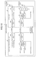
- FIG. 10 is a diagram of a wireless device in which the diversity technique is used.
- a wireless device 2 includes a base band processing unit 30 and an RF-IC unit 40.
- the base band processing unit 30 includes interface units 30a and 30b and a DeMUX processing unit 31.
- the RF-IC unit 40 includes interface units 40a and 40b, as well as a MUX processing unit 41, a DAC 42, and ADCs 43 and 44.
- the signals that have been received by antennas are transferred from the RF-IC unit 40 to the base band processing unit 30 by using one lane.
- the interface unit 30a is a processing unit that, when having obtained IQ data or control data, outputs the IQ data or the control data to the RF- IC unit 40 via a Tx path by converting the obtained data into an LVDS signal.
- the interface unit 30b is a processing unit that receives an LVDS signal from the RF-IC unit 40 via an Rx path and extracts control data, IQ data received by an antenna Ant1, or IQ data received by an antenna Ant2 out of the received signal.
- the interface unit 30b outputs the IQ data received by the antenna Ant1 and the IQ data received by the antenna Ant2 to the DeMUX processing unit 31. Also, the interface unit 30b outputs the control data to an external device.
- the DeMUX processing unit 31 is a processing unit that separates the IQ data that has been received by the antenna Ant1 and the TOD data that has been received by the antenna Ant2 from each other and outputs the separated pieces of IQ data separately.
- the interface unit 40a is a processing unit that, when having obtained an LVDS signal from the base band processing unit 30 via the Tx path, outputs the IQ data contained in the obtained LVDS signal to the DAC 42.
- the interface unit 40b is a processing unit that, when having obtained data that has been output by the MUX processing unit 42 or control data, outputs IQ data or the control data to the base band processing unit 30 via the Rx path by converting the obtained data to an LVDS signal.
- the MUX processing unit 41 is a processing unit that combines the IQ data that has been output by the ADC 43 (i.e., the IQ data that has been received by the antenna Ant1) with the IQ data that has been output by the ADC 44 (i.e., the IQ data that has been received by the antenna Ant2; and outputs the combined data to the interface unit 40b.
- the DAC 42 is a processing unit that converts a digital signal (i.e., IQ data) that has been output by the interface unit 40a into an analog signal and outputs the analog signal resulting from the conversion to the antenna Ant1.
- a digital signal i.e., IQ data
- the ADC 43 is a processing unit that converts an analog signal that has been obtained from the antenna Ant1 into a digital signal (i.e., IQ data) and outputs the digital signal resulting from the conversion to the interface unit 40b.
- the ADC 44 is a processing unit that converts an analog signal that has been obtained from the antenna Ant2 into a digital signal (i.e., IQ data) and outputs the digital signal resulting from the co to the interface unit 40b.
- FIG. 11 is a drawing for explaining a communication format used on an Rx path when a diversity one-lane method is being used.
- LVDS signals on the Rx path in an example in which data has been received by the antenna Ant1 or the antenna Ant2 are illustrated.
- the bit interval between the LVDS signals is the same as the bit interval illustrated in FIG. 8 (i.e., the bit interval is 370 bits).
- LVDS signals on the Rx path in an example in which, while the diversity technique is being used, pieces of IQ data received by the antennas Ant1 and Ant2 are multiplexed and transferred are illustrated.
- the interface unit 40b transfers the pieces of IQ data on the antenna Ant1 side and the pieces of IQ data on the antenna Ant2 side alternately according to the time sequence.
- each of the bit intervals between the LVDS signal is 45 bits, which is shorter than the bit interval that is used when the single reception is performed.
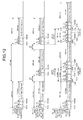
- FIG. 12 is a drawing for explaining the problem of the conventional technique.
- the interval between the LVDS signals each containing IQ data is short.
- inserting the control data causes delays for the IQ data and the control data that follow the inserted control data.
- a wireless device includes a difference calculator that obtains first data received by a first antenna and second data received by a second antenna and calculates a difference value between the first data and the second data; and a transferring unit that transfers the first data and the difference value to a receiving unit.
- a wireless device receives signal waves from a base station by using antennas Ant1 and Ant2
- the wireless device may receive a signal wave from a base station by using one or more antennas other than the antennas Ant1 and Ant2.
- the antennas Ant1 and Ant2 receive mutually the same signal wave from the base station intrinsically, there is no large difference between IQ data received by the antenna Ant1 and IQ data received by the antenna Ant2, and these pieces of IQ data are correlated to each other.
- a main difference between the IQ data received by the antenna Ant1 and the IQ data received by the antenna Ant2 is a phase difference or the like that is caused by using mutually different propagation channels.
- the wireless device calculates, on the RF-IC side, difference values between the IQ data received by the antenna Ant1 and the IQ data received by the antenna Ant2 according to the time sequence and transfers the difference values to the base band processing unit side, instead of the IQ data received the antenna Ant2.
- the wireless device then reconstructs, on the base band processing unit side, the IQ data corresponding to the antenna Ant2 based on the difference values and the IQ data received by the antenna Ant1.
- the data amount of each of the difference values is smaller than that of the IQ data received by the antenna Ant2.
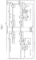
- FIG. 1 is a functional block diagram of a wireless device 100 according to the present embodiment.
- the wireless device 100 includes a base band processing unit 110 and an RF-IC unit 150.
- the base band processing unit 110 and the RF-IC unit 150 are connected to each other by a Tx path and an Rx path, like in the example according to the conventional technique.
- the base band processing unit 110 includes interface units 120a and 120b, as well as a DeMUX processing unit 130, and an IQ data reconstructing unit 140.
- the RF-IC unit 150 includes interface units 150a and 150b, as well as a DAC 160, ADCs 170 and 180, a difference data generating unit 190, and a MUX processing unit 200.
- the interface unit 120a is a processing unit that, when having obtained IQ data or control data, outputs the IQ data (Tx I/Q Data) or the control data (Control Data) to the RF-IC unit 150 via the Tx path by converting the obtained data into an LVDS signal.
- the interface unit 220b is a processing unit that receives an LVDS signal from the RF-IC unit 150 via the Rx path and extracts control data, a difference value (Difference Data), or IQ data (Ant1 Rx I/Q Data) that has been received by the antenna Ant1, out of the received signal.
- the interface unit 120b outputs the IQ data that has been received by the antenna Ant1 to the DeMUX processing unit 130 and outputs the difference value to the IQ data reconstructing unit 140.
- the interface unit 120b outputs the control data to an external device.
- the interface unit 120b In the case where a signal obtained from the interface unit 150b contains IQ data (Ant2 Rx I/Q data) that has been received by the antenna Ant2, the interface unit 120b outputs the IQ data that has been received by the antenna Ant2 to the DeMUX processing unit 130.
- the DeMUX processing unit 130 is a processing unit that, when having received IQ data that has been received the antenna Ant1 from the interface unit 120b, outputs the received IQ data to the IQ data reconstructing unit 140 and to an external device.
- the DeMUX processing unit 130 separates the IQ data received by the antenna Ant1 from the IQ data received by the antenna Ant2. The DeMUX processing unit 130 then outputs the IQ data received by the antenna Ant1 and the IQ data received by the antenna Ant2 to the IQ data reconstructing unit 140 and outputs the IQ data received by the antenna Ant1 to an external device.
- the IQ data reconstructing unit 140 is a processing unit that reconstructs IQ data corresponding to the antenna Ant2, based on IQ data received by the antenna Ant1. and a difference value. For example, the IQ data reconstructing unit 140 reconstructs the IQ data corresponding to the antenna Ant2 by bringing each of the pieces of IQ data (i.e., the pieces of IQ data that are arranged according to the time sequence) received by the antenna Ant1 into correspondence with a different one of the difference values (i.e., the difference values arranged according to the time sequence) at each of different times and adding together the IQ data and the difference value that have been brought into correspondence with each other.
- the pieces of IQ data i.e., the pieces of IQ data that are arranged according to the time sequence
- the difference values i.e., the difference values arranged according to the time sequence
- the IQ data reconstructing unit 140 outputs the IQ data corresponding to the antenna Ant2 that has been reconstructed to an external device. In the case where the IQ data reconstructing unit 140 has obtained IQ data received by the antenna Ant2 from the DeMUX processing unit 130, the IQ data reconstructing unit 140 outputs the obtained IQ data to an external device without performing the reconstructing process.
- the interface unit 150a is a processing unit that, when having obtained an LVDS signal from the base band processing unit 110 via the Tx path, outputs the IQ data contained in the obtained LVDS signal to the DAC 160.
- the interface unit 150b is a processing unit that, when having obtained data output by the MUX processing unit 200, control data, or a difference value, outputs IQ data, the control data, or the difference value to the base band processing unit 110 via the Rx path by converting the obtained data into an LVDS signal.
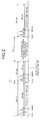
- FIG. 2 is a drawing for explaining a communication format used on the Rx path according to the present embodiment.
- the interface unit 150b stores the IQ data into a payload, appends a sync and a header to the payload, and transfers the with the appendixes to the base band processing unit 110.
- the bit width used for transferring the IQ data received by the antenna Ant1 is 280 bits.
- the interface unit 150b When having obtained a difference value, the interface unit 150b stores the difference value into a payload having 128 bits, appends a sync and a header to the payload, and transfers the payload with the appendixes to the base band processing unit 110.
- the bit width used for transferring the difference value is 152 bits.
- the interface unit 150b transfers the LVDS signals each storing therein IQ data and the LVDS signals each storing therein a difference value alternately. As illustrated in FIG. 2 , the interface unit 150b transmits an LVDS signal storing IQ data therein with a 172-bit interval after transferring an LVDS signal storing therein a difference value. When a bit width of 172 bits like this is present, it is possible to transfer an LVDS signal (56 bits) corresponding to the control data to the base band processing unit 110 without delaying the transfer of the IQ data or the transfer of the difference value.
- the interface unit 150b When having obtained IQ data received by the antenna Ant1 and IQ data received by the antenna Ant2 from the MUX processing unit 200, the interface unit 150b transfers the pieces of IQ data on the antenna Ant1 side and the pieces of IQ data on the antenna Ant2 side alternately according to the time sequence, like in the conventional wireless device.
- the DAC 160 is a processing unit that converts a digital signal (i.e., IQ data) that has been output by the interface unit 150a into an analog signal and outputs the analog signal resulting from the conversion to the antenna Ant1.
- a digital signal i.e., IQ data
- the ADC 170 is a processing unit that converts an analog signal that has been obtained from the antenna Ant1 into a digital signal (i.e., IQ data) and outputs the digital signal resulting from the conversion to the MUX processing unit 200 and to the difference data generating unit 190.
- the ADC 180 is a processing unit that converts an analog signal that has been obtained from the antenna Ant2 into a digital signal (i.e., IQ data) and outputs the digital signal resulting from the conversion to the difference data generating unit 190.
- the difference data generating unit 190 is a processing unit that calculates a difference value between IQ data that has been obtained from the ADC 170 and IQ data that has been obtained from the ADC 180 for each of different times and outputs the calculated difference value to the interface unit 150b. In the case where the data amount of the difference value is equal to or larger than a threshold value, the difference data generating unit 190 outputs the IQ data that has been received by the antenna Ant2 to the MUX processing unit 200, instead of the difference value.
- the MUX processing unit 200 In the case where the MUX processing unit 200 has obtained only IQ data, received by the antenna Ant1 from the ADC 170, the MUX processing unit 200 outputs the IQ data received by the antenna Ant1 to the interface unit 150b. In the case where the MUX processing unit 200 has obtained IQ data received by the antenna Ant1 from the ADC 170 and has obtained IQ data received by the antenna Ant2 from the difference data generating unit 19G, the MUX processing unit 200 combines the pieces of IQ data together and outputs the combined pieces of IQ data to the interface unit 150b.
- FIG. 3 is a diagram of the difference data generating unit 190.
- the difference data generating unit 190 includes a difference calculator 191, a difference threshold comparing unit 192, a binarizing unit 193, and a transmission selection processing unit 194.
- the difference calculator 191 is a processing unit that calculates the difference value between the IQ data that has been obtained from the ADC 170 and the IQ data that has been obtained from the ADC 180 for each of the different times and outputs the calculated difference value to the difference threshold comparing unit 192 and the binarizing unit 193.
- the difference threshold comparing unit 192 is a processing unit that compares the data amount of each of the difference values with the threshold value and judges whether the data amount of each of the difference values is equal to or larger than the threshold value.
- the threshold value is assumed to be, for instance, 128 bits.
- the difference threshold comparing unit 192 outputs a comparison result to the transmission selection processing unit 194.
- the binarizing unit 193 is a processing unit that, when having obtained a difference value from the difference calculator 191, converts the obtained difference value into bits.
- the binarizing unit 193 transmits the difference value that has been converted into the bits to the transmission selection processing unit 194.
- the transmission selection processing unit 194 is a processing unit that, based on a comparison result from the difference threshold comparing unit 192, outputs a difference value or IQ data received by the antenna Ant2 to the interface unit 150b. Mere specifically, in the case where the data amount of the difference value is equal to or large than the threshold value, the transmission selection processing unit 194 outputs the IQ data received by the antenna Ant2 to the interface unit 150b. In contrast, in the case where the data amount of the difference value is smaller than the threshold value, the transmission selection processing unit 194 outputs the difference value to the interface unit 150b.
- FIG. 4 is a diagram of the IQ data reconstructing unit 140. As illustrated in FIG. 4 , the IQ data reconstructing unit 140 includes a reconstruction processing unit 141 and a selection processing unit 142.
- the reconstruction processing unit 141 is a processing unit that reconstructs IQ data corresponding to the antenna Ant2 based on IQ data received by the antenna Ant1 and a difference value. For example, the reconstruction processing unit 141 reconstructs the IQ data corresponding to the antenna Ant2 by bringing each of the pieces of IQ data (i.e., the pieces of IQ data arranged according to the time sequence) received by the antenna Ant1 into correspondence with a different one of the difference values (i.e., the difference values arranged according to the time sequence) at each of the different times and adding together the IQ data and the difference value that have been brought into correspondence with each other. The reconstruction processing unit 141 outputs the IQ data corresponding to the antenna Ant2 that has been reconstructed to the selection processing unit 142.
- the selection processing unit 142 is a processing unit that selects one between the IQ data corresponding to the antenna Ant2 that has been output by the reconstruction processing unit 141 and the IQ data received by the antenna Ant2 that has been output by the DeMUX processing unit 130 and outputs the selected IQ data to the external device as the IQ data for the antenna Ant2.
- the selection processing unit 142 In the case where the selection processing unit 142 has obtained the IQ data received by the antenna Ant2 from the DeMUX processing unit 130, the selection processing unit 142 outputs the IQ data to the external device. In contrast, in the case where the selection processing unit 142 is not able to obtain the IQ data received by the antenna Ant2 from the DeMUX processing unit 130, the selection processing unit 142 obtains the IQ data corresponding to the antenna Ant2 from the reconstruction processing unit 141 and outputs the IQ data to the external devise.
- Fig. 5 is a flowchart of the processing procedure performed by the RF-IC unit 150 according to the present embodiment.
- the RF-IC unit 150 obtains IQ data received by the antenna Ant1 and IQ data received by the antenna Ant2 (step S101) and calculates a difference value between the pieces of IQ data (step S102).
- the RF-IC unit 150 judges whether the data amount of the difference value is equal to or larger than the threshold value (step S103). In the case where the data amount of the difference value is smaller than the threshold value (step S104: No), the RF-IC unit 150 outputs the IQ data received by the antenna Ant1 and the difference value to the base band processing unit 110 (step S105). In contrast, in the case where the data amount of the difference value is equal to or larger than the threshold value (step S104: Yes), the RF-IC unit 150 outputs the IQ data received by the antenna Ant1 and the IQ data received by the antenna Ant2 to the base band processing unit 110 (step S106).
- FIG. 6 is a flowchart of the processing procedure performed by the IQ data reconstructing unit 140 according to the present embodiment. As illustrated in FIG. 6 , the IQ data reconstructing unit 140 judges whether a difference value has been obtained (step S201).
- the IQ data reconstructing unit 140 reconstructs the IQ data corresponding to the antenna Ant2 based on the difference value and the IQ data received by the antenna Ant1 (step S203) and outputs the IQ data for the antenna Ant2 (step S204).
- step S202 the IQ data reconstructing unit 140 obtains the IQ data received by the antenna Ant2 from the DeMUX processing unit 130 (step S205), and the process proceeds to step S204.
- the wireless device 100 is configured so that the RF-IC unit 150 calculates the difference value between the IQ data received by the antenna Ant1 and the IQ data received by the antenna Ant2 and transfers the difference value to the base band processing unit 110, instead of the IQ data received by the antenna Ant2.
- the wireless device 100 is further configured so that the base band processing unit 110 reconstructs the IQ data corresponding to the antenna Ant2, based an the difference value and the IQ data received by the antenna Ant1.
- the data amount of each of the difference values is smaller than that of the IQ data received by the antenna Ant2.
- the wireless device according to an aspect of the present invention When the wireless device according to an aspect of the present invention is being used, it is possible to prevent data delays even if the pieces of data that have been received by the plurality of antennas are transferred by using one lane.
Landscapes
- Engineering & Computer Science (AREA)
- Computer Networks & Wireless Communication (AREA)
- Signal Processing (AREA)
- Mobile Radio Communication Systems (AREA)
- Radio Transmission System (AREA)
- Digital Transmission Methods That Use Modulated Carrier Waves (AREA)
- Circuits Of Receivers In General (AREA)
- Transceivers (AREA)
Abstract
Description
- The embodiment discussed herein is directed to a wireless device.
- An interface standard specification called DigRF has recently been established in the field of portable terminals and the like. DigRF is a specification that defines mutual connectivity between a base band processing unit and a Radio-Frequency Integrated-Circuit (RF-IC) unit that are included in a portable terminal.
FIG. 7 is a diagram of a wireless device that is compliant with a DigRF v3 specification. - As illustrated in
FIG. 7 , awireless device 1 includes a baseband processing unit 10 and an RF-IC unit 20. The baseband processing unit 10 includesinterface units IC unit 20 includesinterface units - The
interface units IC unit 20 via a Tx path and an Rx path, respectively. When transmitting and receiving the IQ data and the control data, theinterface units - The
interface units band processing unit 10 via the Tx path and the Rx path, respectively. When transmitting and receiving the IQ data and the control data, theinterface units - When having obtained the IQ data from the base
band processing unit 10 via the Tx path, theinterface unit 20a outputs the obtained IQ data to theDAC 21. When having obtained the IQ data from theADC 22, theinterface unit 20b outputs the IQ data to the baseband processing unit 10 via the Rx path. - The
DAC 21 is a processing unit that converts a digital signal (i.e., IQ data) that has been output from theinterface unit 20a into an analog signal any outputs the analog signal resulting from the conversion to an antenna. TheADC 22 converts an analog signal obtained from the antenna into a digital signal (i.e., IQ data) and outputs the digital signal resulting from the conversion to theinterface unit 20b. - Next, communication formats used on the Tx path and the Rx path will be explained.
FIG. 8 is a drawing for explaining communication formats used on the conventional Tx path and the conventional Rx path. Data transferred on the Tx path and the Rx path includes a sync, a header, and a payload. Of these, the sync is a set of pattern bits made up of 16 bits and is used for detecting a synchronization. The header is a set of heading bits made up of 8 bits and is used for informing the type of data. - The payload is a set of data bits made up of a number of bits ranging from 8 bits to 512 bits. When transferring IQ data on the Tx path or the Rx path, the corresponding one of the interface units stores the IQ data into a payload. According to the DigRF v3 specification, the bit size of a payload on the Tx path is defined as 96 bits, whereas the bit size of a payload on the Rx path is defined as 256 bits. As illustrated in the upper portion of
FIG. 8 , when IQ data is transmitted on the Tx path, the IQ data is transferred in pieces of data each having 120 bits. Also, as illustrated in the middle portion ofFIG. 8 , when the IQ data is transmitted on the Rx path, the IQ data is transferred in pieces of data each having 280 bits. - Further, when transmitting the control data on the Tax path or the Rx path, the corresponding one of the interface units stores the control data into a payload. When storing the control data into a payload, the bit size of the payload is, for example, 32 bits.
- As illustrated in the lower portion of
FIG. 8 , the interface unit transfers a piece of control data between two pieces of IQ data. In the case where the timing with which a piece of IQ data is transferred and the timing with which a piece of control data is transferred overlap each other, the interface unit waits until the transfer of the first piece of data is completed before transferring the second piece of data. - Next, a configuration of the
interface units FIG. 7 will be explained.FIG. 9 is a diagram of the conventional interface units. As illustrated inFIG. 9 , theinterface unit 10a includes a MUX processing unit 11, a Parallel/Serial (P/S) conversion processing unit 12, a sync MUX processing unit 13, and anLVDS driver 14. Theinterface unit 10b includes anLVDS receiver 15, asampling processing unit 16, a sync detection processing unit 17, a Serial/Parallel (S/P)conversion processing unit 18, and adetection processing unit 19. - The MUX processing unit 11 is a processing unit that, when having obtained IQ data and control data, multiplexes the IQ data and the control data that have been obtained. The MUX processing unit 11 outputs the multiplexed data to the P/S conversion processing unit 12.
- The P/S conversion processing unit 12 is a processing unit that, when having obtained multiplexed data from the MUX Processing unit 11, performs a serial conversion process. The P/S conversion processing unit 12 outputs the data on which the serial conversion process has been performed to the sync MUX processing unit 13.
- The sync MUX Processing unit 13 is a processing unit that, when having obtained data on which a serial conversion process has been performed from the P/S conversion processing unit 12, appends a sync to the obtained data. The sync MUX processing unit 13 outputs the data to which the sync has been appended to the
LVDS driver 14. - The
LVDS driver 14 is a processing unit that, when having obtained data to which a sync has been appended from the sync MUX processing unit 13, converts the obtained data into an LVDS signal. In this situation, the LVDS signal contains a sync, a header, and a payload that are illustrated inFIG. 8 . The LVDS driver 14 transfers data by storing IQ data or control data into a payload. - The
LVDS receiver 15 is a processing unit that receives an LVDS signal from the RF-IC unit 20 and converts the received LIDS signal into a single signal. The LVDSreceiver 15 outputs the single signal resulting from the conversion to thesampling processing unit 16. - The
sampling processing unit 16 is a processing unit that, when having obtained a single signal from theLVDS receiver 15, performs a sampling process on the single signal. Thesampling processing unit 16 outputs the data that is a result of the sampling process to the sync detection processing unit 17. - The sync detection processing unit 17 is a processing unit that, when having obtained the data that is a result of the sampling process from the
sampling processing unit 16, detects the sync in the obtained data and performs a synchronization process by comparing and matching the detected sync with a sync pattern defined by the DigRF v3 specification. The sync detection processing unit 17 outputs the data on which the synchronization process has been performed to the S/Pconversion processing unit 18. - The S/P
conversion processing unit 18 is a processing unit that, when having obtained data from the sync detection processing unit 17, performs a parallel conversion process on the obtained data. The S/Pconversion processing unit 18 outputs the data on which the parallel conversion process has been performed to thedetection processing unit 19. - When having obtained data from the S/P
conversion processing unit 18, thedetection processing unit 19 analyzes the header contained in the obtained data and extracts the IQ data (Rx I/Q Data) or the control data (RF-IC Response) that is stored in the payload within the data. Thedetection processing unit 19 outputs IQ data and control data separately to an external device. - As another example, besides the
wireless device 1 illustrated inFIG. 7 , a wireless device that utilizes a technique called "diversity" has been proposed. For example, diversity is a technique by which, among mutually the same wireless signals that have been received by a plurality of antennas, the signal that has been received by the antenna having a better radio wave condition is used with a higher priority. -
FIG. 10 is a diagram of a wireless device in which the diversity technique is used. As illustrated inFIG. 10 , awireless device 2 includes a base band processing unit 30 and an RF-IC unit 40. The base band processing unit 30 includesinterface units processing unit 31. The RF-IC unit 40 includesinterface units MUX processing unit 41, aDAC 42, andADCs wireless device 2 illustrated inFIG. 10 , the signals that have been received by antennas are transferred from the RF-IC unit 40 to the base band processing unit 30 by using one lane. - The
interface unit 30a is a processing unit that, when having obtained IQ data or control data, outputs the IQ data or the control data to the RF-IC unit 40 via a Tx path by converting the obtained data into an LVDS signal. - The
interface unit 30b is a processing unit that receives an LVDS signal from the RF-IC unit 40 via an Rx path and extracts control data, IQ data received by an antenna Ant1, or IQ data received by an antenna Ant2 out of the received signal. Theinterface unit 30b outputs the IQ data received by the antenna Ant1 and the IQ data received by the antenna Ant2 to theDeMUX processing unit 31. Also, theinterface unit 30b outputs the control data to an external device. - The
DeMUX processing unit 31 is a processing unit that separates the IQ data that has been received by the antenna Ant1 and the TOD data that has been received by the antenna Ant2 from each other and outputs the separated pieces of IQ data separately. - The
interface unit 40a is a processing unit that, when having obtained an LVDS signal from the base band processing unit 30 via the Tx path, outputs the IQ data contained in the obtained LVDS signal to theDAC 42. - The
interface unit 40b is a processing unit that, when having obtained data that has been output by theMUX processing unit 42 or control data, outputs IQ data or the control data to the base band processing unit 30 via the Rx path by converting the obtained data to an LVDS signal. - The
MUX processing unit 41 is a processing unit that combines the IQ data that has been output by the ADC 43 (i.e., the IQ data that has been received by the antenna Ant1) with the IQ data that has been output by the ADC 44 (i.e., the IQ data that has been received by the antenna Ant2; and outputs the combined data to theinterface unit 40b. - The
DAC 42 is a processing unit that converts a digital signal (i.e., IQ data) that has been output by theinterface unit 40a into an analog signal and outputs the analog signal resulting from the conversion to the antenna Ant1. - The
ADC 43 is a processing unit that converts an analog signal that has been obtained from the antenna Ant1 into a digital signal (i.e., IQ data) and outputs the digital signal resulting from the conversion to theinterface unit 40b. TheADC 44 is a processing unit that converts an analog signal that has been obtained from the antenna Ant2 into a digital signal (i.e., IQ data) and outputs the digital signal resulting from the co to theinterface unit 40b. -
FIG. 11 is a drawing for explaining a communication format used on an Rx path when a diversity one-lane method is being used. In the upper portion ofFIG. 11 , LVDS signals on the Rx path in an example in which data has been received by the antenna Ant1 or the antenna Ant2 are illustrated. When a single reception like in the present example is performed, the bit interval between the LVDS signals is the same as the bit interval illustrated inFIG. 8 (i.e., the bit interval is 370 bits). - In the lower portion of
FIG. 11 , LVDS signals on the Rx path in an example in which, while the diversity technique is being used, pieces of IQ data received by the antennas Ant1 and Ant2 are multiplexed and transferred are illustrated. As illustrated in the lower portion ofFIG. 11 , when the diversity cne-lane method is being used, theinterface unit 40b transfers the pieces of IQ data on the antenna Ant1 side and the pieces of IQ data on the antenna Ant2 side alternately according to the time sequence. Also, each of the bit intervals between the LVDS signal is 45 bits, which is shorter than the bit interval that is used when the single reception is performed. - The conventional technique as described above is disclosed in for example Japanese Laid-cpen Patent Publication No.
2007-28569 - Publication No.
2007-96762 - The conventional wireless device described above, however, has a problem where data delays are caused when pieces of IQ data that have been received by the plurality of antennas and the control data are transferred by using one lane.
FIG. 12 is a drawing for explaining the problem of the conventional technique. - As illustrated in the lower portion of
FIG. 12 , when the diversity one-lane method is being used, the interval between the LVDS signals each containing IQ data is short. Thus, it is not possible to just insert and transfer control data. Accordingly, to transfer the control data, it is necessary to secure a bit width that allows the control data to be inserted by delaying the LVDS signals each containing the IQ data. As understood from comparing the middle portion ofFIG. 12 with the lower portion ofFIG. 12 , inserting the control data causes delays for the IQ data and the control data that follow the inserted control data. - When data delays like the ones illustrated in PIG. 12 are caused, there is a possibility that, for example, a delay may be caused for the control data transferred from the reception side to the transmission, side, and also, a buffer overflow may be caused on the transmission side where a certain process is performed after the control data has been received. For this reason, it is an important goal to solve the problem of data delays.
- Accordingly, it is considered desirable to provide a wireless device that is capable of solving the problem of data delays.
- According to an aspect of an embodiment of the invention, a wireless device includes a difference calculator that obtains first data received by a first antenna and second data received by a second antenna and calculates a difference value between the first data and the second data; and a transferring unit that transfers the first data and the difference value to a receiving unit.
-
-
FIG. 1 is a functional block diagram of a wireless device according to an embodiment of the present invention; -
FIG. 2 is a drawing for explaining a communication format used on an Rx path according to the embodiment; -
FIG. 3 is a diagram of a difference data generating unit; -
FIG. 4 is a diagram of an IQ data reconstructing unit; -
FIG. 5 is a flowchart of a processing procedure performed by an RF-IC unit according to the embodiment; -
FIG. 6 is a flowchart of a processing procedure performed by the IQ data reconstructing unit according to the embodiment; -
FIG. 7 is a diagram of a wireless device that is compliant with a DigRF v3 specification; -
FIG. 8 is a drawing for explaining communication formats used on a conventional Tx path and a conventional Rx path; -
FIG. 9 is a diagram of conventional interface units; -
FIG. 10 is a diagram of a wireless device in which a diversity technique is used; -
FIG. 11 is a drawing for explaining a communication format used on an Rx path when a diversity one-lane method is being used; and -
FIG. 12 is a drawing for explaining a problem of a conventional technique. - A preferred embodiment of the present invention will be explained with reference to accompanying drawings. The present invention is not limited to the exemplary embodiment.
- In the following sections, an example in which a wireless device receives signal waves from a base station by using antennas Ant1 and Ant2 will be explained; however, the present invention is not limited to this example. The wireless device may receive a signal wave from a base station by using one or more antennas other than the antennas Ant1 and Ant2.
- First, an overview of the wireless device according to the present embodiment will be explained. Because the antennas Ant1 and Ant2 receive mutually the same signal wave from the base station intrinsically, there is no large difference between IQ data received by the antenna Ant1 and IQ data received by the antenna Ant2, and these pieces of IQ data are correlated to each other. A main difference between the IQ data received by the antenna Ant1 and the IQ data received by the antenna Ant2 is a phase difference or the like that is caused by using mutually different propagation channels.
- Thus, the wireless device according to the present embodiment calculates, on the RF-IC side, difference values between the IQ data received by the antenna Ant1 and the IQ data received by the antenna Ant2 according to the time sequence and transfers the difference values to the base band processing unit side, instead of the IQ data received the antenna Ant2. The wireless device then reconstructs, on the base band processing unit side, the IQ data corresponding to the antenna Ant2 based on the difference values and the IQ data received by the antenna Ant1.
- The data amount of each of the difference values is smaller than that of the IQ data received by the antenna Ant2. Thus, even if the wireless device is configured so that pieces of IQ data received by a plurality of antennas and control data are transferred by using one lane, it is possible to secure a bit width for the control data. Consequently, it is possible to prevent data delays.
- Next, a configuration of the wireless device according to the present embodiment will be explained.
FIG. 1 is a functional block diagram of awireless device 100 according to the present embodiment. As illustrated inFIG. 1 , thewireless device 100 includes a baseband processing unit 110 and an RF-IC unit 150. The baseband processing unit 110 and the RF-IC unit 150 are connected to each other by a Tx path and an Rx path, like in the example according to the conventional technique. - The base
band processing unit 110 includesinterface units DeMUX processing unit 130, and an IQdata reconstructing unit 140. The RF-IC unit 150 includesinterface units DAC 160,ADCs data generating unit 190, and aMUX processing unit 200. - Next, processing units included in the base
band processing unit 110 will be explained. Theinterface unit 120a is a processing unit that, when having obtained IQ data or control data, outputs the IQ data (Tx I/Q Data) or the control data (Control Data) to the RF-IC unit 150 via the Tx path by converting the obtained data into an LVDS signal. - The interface unit 220b is a processing unit that receives an LVDS signal from the RF-
IC unit 150 via the Rx path and extracts control data, a difference value (Difference Data), or IQ data (Ant1 Rx I/Q Data) that has been received by the antenna Ant1, out of the received signal. Theinterface unit 120b outputs the IQ data that has been received by the antenna Ant1 to theDeMUX processing unit 130 and outputs the difference value to the IQdata reconstructing unit 140. Theinterface unit 120b outputs the control data to an external device. - In the case where a signal obtained from the
interface unit 150b contains IQ data (Ant2 Rx I/Q data) that has been received by the antenna Ant2, theinterface unit 120b outputs the IQ data that has been received by the antenna Ant2 to theDeMUX processing unit 130. - The
DeMUX processing unit 130 is a processing unit that, when having received IQ data that has been received the antenna Ant1 from theinterface unit 120b, outputs the received IQ data to the IQdata reconstructing unit 140 and to an external device. - In the case where data received from the
interface unit 120b contains both IQ data received by the antenna Ani1 and IQ data received by the antenna Ant2, theDeMUX processing unit 130 separates the IQ data received by the antenna Ant1 from the IQ data received by the antenna Ant2. TheDeMUX processing unit 130 then outputs the IQ data received by the antenna Ant1 and the IQ data received by the antenna Ant2 to the IQdata reconstructing unit 140 and outputs the IQ data received by the antenna Ant1 to an external device. - The IQ
data reconstructing unit 140 is a processing unit that reconstructs IQ data corresponding to the antenna Ant2, based on IQ data received by the antenna Ant1. and a difference value. For example, the IQdata reconstructing unit 140 reconstructs the IQ data corresponding to the antenna Ant2 by bringing each of the pieces of IQ data (i.e., the pieces of IQ data that are arranged according to the time sequence) received by the antenna Ant1 into correspondence with a different one of the difference values (i.e., the difference values arranged according to the time sequence) at each of different times and adding together the IQ data and the difference value that have been brought into correspondence with each other. - The IQ
data reconstructing unit 140 outputs the IQ data corresponding to the antenna Ant2 that has been reconstructed to an external device. In the case where the IQdata reconstructing unit 140 has obtained IQ data received by the antenna Ant2 from theDeMUX processing unit 130, the IQdata reconstructing unit 140 outputs the obtained IQ data to an external device without performing the reconstructing process. - Next, processing units included in the RF-
IC unit 150 will be explained. Theinterface unit 150a is a processing unit that, when having obtained an LVDS signal from the baseband processing unit 110 via the Tx path, outputs the IQ data contained in the obtained LVDS signal to theDAC 160. - The
interface unit 150b is a processing unit that, when having obtained data output by theMUX processing unit 200, control data, or a difference value, outputs IQ data, the control data, or the difference value to the baseband processing unit 110 via the Rx path by converting the obtained data into an LVDS signal. -
FIG. 2 is a drawing for explaining a communication format used on the Rx path according to the present embodiment. When having obtained the IQ data received by the antenna Ant1, theinterface unit 150b stores the IQ data into a payload, appends a sync and a header to the payload, and transfers the with the appendixes to the baseband processing unit 110. The bit width used for transferring the IQ data received by the antenna Ant1 is 280 bits. - When having obtained a difference value, the
interface unit 150b stores the difference value into a payload having 128 bits, appends a sync and a header to the payload, and transfers the payload with the appendixes to the baseband processing unit 110. The bit width used for transferring the difference value is 152 bits. - As illustrated in
FIG. 2 , theinterface unit 150b transfers the LVDS signals each storing therein IQ data and the LVDS signals each storing therein a difference value alternately. As illustrated inFIG. 2 , theinterface unit 150b transmits an LVDS signal storing IQ data therein with a 172-bit interval after transferring an LVDS signal storing therein a difference value. When a bit width of 172 bits like this is present, it is possible to transfer an LVDS signal (56 bits) corresponding to the control data to the baseband processing unit 110 without delaying the transfer of the IQ data or the transfer of the difference value. - When having obtained IQ data received by the antenna Ant1 and IQ data received by the antenna Ant2 from the
MUX processing unit 200, theinterface unit 150b transfers the pieces of IQ data on the antenna Ant1 side and the pieces of IQ data on the antenna Ant2 side alternately according to the time sequence, like in the conventional wireless device. - The
DAC 160 is a processing unit that converts a digital signal (i.e., IQ data) that has been output by theinterface unit 150a into an analog signal and outputs the analog signal resulting from the conversion to the antenna Ant1. - The
ADC 170 is a processing unit that converts an analog signal that has been obtained from the antenna Ant1 into a digital signal (i.e., IQ data) and outputs the digital signal resulting from the conversion to theMUX processing unit 200 and to the differencedata generating unit 190. TheADC 180 is a processing unit that converts an analog signal that has been obtained from the antenna Ant2 into a digital signal (i.e., IQ data) and outputs the digital signal resulting from the conversion to the differencedata generating unit 190. - The difference
data generating unit 190 is a processing unit that calculates a difference value between IQ data that has been obtained from theADC 170 and IQ data that has been obtained from theADC 180 for each of different times and outputs the calculated difference value to theinterface unit 150b. In the case where the data amount of the difference value is equal to or larger than a threshold value, the differencedata generating unit 190 outputs the IQ data that has been received by the antenna Ant2 to theMUX processing unit 200, instead of the difference value. - In the case where the
MUX processing unit 200 has obtained only IQ data, received by the antenna Ant1 from theADC 170, theMUX processing unit 200 outputs the IQ data received by the antenna Ant1 to theinterface unit 150b. In the case where theMUX processing unit 200 has obtained IQ data received by the antenna Ant1 from theADC 170 and has obtained IQ data received by the antenna Ant2 from the difference data generating unit 19G, theMUX processing unit 200 combines the pieces of IQ data together and outputs the combined pieces of IQ data to theinterface unit 150b. - Next, a configuration of the difference
data generating unit 190 illustrated inFIG. 1 will be explained.FIG. 3 is a diagram of the differencedata generating unit 190. As illustrated inFIG. 3 , the differencedata generating unit 190 includes adifference calculator 191, a differencethreshold comparing unit 192, abinarizing unit 193, and a transmissionselection processing unit 194. - The
difference calculator 191 is a processing unit that calculates the difference value between the IQ data that has been obtained from theADC 170 and the IQ data that has been obtained from theADC 180 for each of the different times and outputs the calculated difference value to the differencethreshold comparing unit 192 and thebinarizing unit 193. - The difference
threshold comparing unit 192 is a processing unit that compares the data amount of each of the difference values with the threshold value and judges whether the data amount of each of the difference values is equal to or larger than the threshold value. In the present example, the threshold value is assumed to be, for instance, 128 bits. The differencethreshold comparing unit 192 outputs a comparison result to the transmissionselection processing unit 194. - The
binarizing unit 193 is a processing unit that, when having obtained a difference value from thedifference calculator 191, converts the obtained difference value into bits. Thebinarizing unit 193 transmits the difference value that has been converted into the bits to the transmissionselection processing unit 194. - The transmission
selection processing unit 194 is a processing unit that, based on a comparison result from the differencethreshold comparing unit 192, outputs a difference value or IQ data received by the antenna Ant2 to theinterface unit 150b. Mere specifically, in the case where the data amount of the difference value is equal to or large than the threshold value, the transmissionselection processing unit 194 outputs the IQ data received by the antenna Ant2 to theinterface unit 150b. In contrast, in the case where the data amount of the difference value is smaller than the threshold value, the transmissionselection processing unit 194 outputs the difference value to theinterface unit 150b. - Next, a configuration of the IQ
data reconstructing unit 140 illustrated inFIG. 1 will be explained.FIG. 4 is a diagram of the IQdata reconstructing unit 140. As illustrated inFIG. 4 , the IQdata reconstructing unit 140 includes areconstruction processing unit 141 and aselection processing unit 142. - The
reconstruction processing unit 141 is a processing unit that reconstructs IQ data corresponding to the antenna Ant2 based on IQ data received by the antenna Ant1 and a difference value. For example, thereconstruction processing unit 141 reconstructs the IQ data corresponding to the antenna Ant2 by bringing each of the pieces of IQ data (i.e., the pieces of IQ data arranged according to the time sequence) received by the antenna Ant1 into correspondence with a different one of the difference values (i.e., the difference values arranged according to the time sequence) at each of the different times and adding together the IQ data and the difference value that have been brought into correspondence with each other. Thereconstruction processing unit 141 outputs the IQ data corresponding to the antenna Ant2 that has been reconstructed to theselection processing unit 142. - The
selection processing unit 142 is a processing unit that selects one between the IQ data corresponding to the antenna Ant2 that has been output by thereconstruction processing unit 141 and the IQ data received by the antenna Ant2 that has been output by theDeMUX processing unit 130 and outputs the selected IQ data to the external device as the IQ data for the antenna Ant2. - In the case where the
selection processing unit 142 has obtained the IQ data received by the antenna Ant2 from theDeMUX processing unit 130, theselection processing unit 142 outputs the IQ data to the external device. In contrast, in the case where theselection processing unit 142 is not able to obtain the IQ data received by the antenna Ant2 from theDeMUX processing unit 130, theselection processing unit 142 obtains the IQ data corresponding to the antenna Ant2 from thereconstruction processing unit 141 and outputs the IQ data to the external devise. - Next, a processing procedure performed by the RF-
IC unit 150 according to the present embodiment will be explained.Fig. 5 is a flowchart of the processing procedure performed by the RF-IC unit 150 according to the present embodiment. As illustrated inFIG. 5 , the RF-IC unit 150 obtains IQ data received by the antenna Ant1 and IQ data received by the antenna Ant2 (step S101) and calculates a difference value between the pieces of IQ data (step S102). - The RF-
IC unit 150 then judges whether the data amount of the difference value is equal to or larger than the threshold value (step S103). In the case where the data amount of the difference value is smaller than the threshold value (step S104: No), the RF-IC unit 150 outputs the IQ data received by the antenna Ant1 and the difference value to the base band processing unit 110 (step S105). In contrast, in the case where the data amount of the difference value is equal to or larger than the threshold value (step S104: Yes), the RF-IC unit 150 outputs the IQ data received by the antenna Ant1 and the IQ data received by the antenna Ant2 to the base band processing unit 110 (step S106). - Next, a processing procedure performed by the IQ
data reconstructing unit 140 according to the present embodiment will be explained.FIG. 6 is a flowchart of the processing procedure performed by the IQdata reconstructing unit 140 according to the present embodiment. As illustrated inFIG. 6 , the IQdata reconstructing unit 140 judges whether a difference value has been obtained (step S201). - In the case where a difference value has been obtained (step S202: Yes), the IQ
data reconstructing unit 140 reconstructs the IQ data corresponding to the antenna Ant2 based on the difference value and the IQ data received by the antenna Ant1 (step S203) and outputs the IQ data for the antenna Ant2 (step S204). - In contrast, in the case where the difference value has not been obtained (step S202: No), the IQ
data reconstructing unit 140 obtains the IQ data received by the antenna Ant2 from the DeMUX processing unit 130 (step S205), and the process proceeds to step S204. - As explained above, the
wireless device 100 according to the present embodiment is configured so that the RF-IC unit 150 calculates the difference value between the IQ data received by the antenna Ant1 and the IQ data received by the antenna Ant2 and transfers the difference value to the baseband processing unit 110, instead of the IQ data received by the antenna Ant2. Thewireless device 100 is further configured so that the baseband processing unit 110 reconstructs the IQ data corresponding to the antenna Ant2, based an the difference value and the IQ data received by the antenna Ant1. - The data amount of each of the difference values is smaller than that of the IQ data received by the antenna Ant2. Thus, even if the pieces of IQ data received by the plurality of antennas and the control data are transferred by using one lane within the
wireless device 100, it is possible to secure a bit width for the control data. As a result, it is possible to prevent data delays. - Of the various processes explained in the description of the embodiment, it is acceptable to manually perform all or a part of the processes that are described as being automatically performed. Conversely, it is acceptable to automatically perform, by using a publicly known method, all or a part of the processes that are described as being manually performed. In addition, it is acceptable to arbitrarily apply a modification to any of the processing procedures, the controlling procedures, the specific names, and the information including the various types of data and the various parameters that are illustrated in the text above and the drawings, unless otherwise noted.
- When the wireless device according to an aspect of the present invention is being used, it is possible to prevent data delays even if the pieces of data that have been received by the plurality of antennas are transferred by using one lane.
Claims (10)
- A wireless device (100) comprising:a difference calculator (191) that obtains first data received by a first antenna and second data received by a second antenna and calculates a difference value between the first data and the second data; anda transferring unit (192, 193, 194) that transfers the first data and the difference value to a receiving unit.
- The wireless device (100) according to claim 1, wherein the transferring unit (192, 193, 194) converts the first data and the difference value into signals and transfers the signals resulting from the conversion alternately to the receiving unit.
- The wireless device (100) according to claim 1 or 2, wherein the transferring unit (192, 193, 194) compares a data amount of the difference value and a threshold value, and the transferring unit (192, 193, 194) transfers the first data and the difference value to the receiving unit if the data amount of the difference value is smaller than the threshold value.
- The wireless device (100) according to any one of claims 1 to 3, wherein the transferring unit (192, 193, 194) compares a data amount of the difference value and a threshold value, and the transferring unit (192, 193, 194) transmits the second data instead of the difference value if the data amount of the difference value is equal to or larger than the threshold value.
- The wireless device (100) according to any one of claims 1 to 4, further comprising a reconstructing unit (140) that, when the first data and the difference value from the transferring unit (192, 193, 194) are received, reconstructs the second data, based on the first data and the difference value.
- A transferring method performed in a wireless device (100) comprising:obtaining first data received by a first antenna and second data received by a second antenna;calculating a difference value between the first data and the second data; andtransferring the first data and the difference value to a receiving unit.
- The transferring method according to claim 6, wherein the transferring includes converting the first data and the difference value into signals and transferring the signals resulting from the conversion alternately to the receiving unit.
- The transferring method according to claim 6 or 7, wherein the transferring includes:comparing a data amount of the difference value and a threshold value; andtransferring the first data and the difference value to the receiving unit if the data amount of the difference value is smaller than the threshold value.
- The transferring method according to any one of claims 6 to 8, wherein the transferring includes:comparing a data amount of the difference value and a threshold value; andtransmitting the second data instead of the difference value if the data amount of the difference value is equal to or larger than the threshold value.
- The transferring method according to any one of claims 6 to 9, further comprising:reconstructing, when the first data and the difference value are received, the second data based on the first data and the difference value.
Applications Claiming Priority (1)
| Application Number | Priority Date | Filing Date | Title |
|---|---|---|---|
| JP2009120191A JP5347709B2 (en) | 2009-05-18 | 2009-05-18 | Wireless device |
Publications (3)
| Publication Number | Publication Date |
|---|---|
| EP2254256A2 true EP2254256A2 (en) | 2010-11-24 |
| EP2254256A3 EP2254256A3 (en) | 2014-01-01 |
| EP2254256B1 EP2254256B1 (en) | 2017-04-19 |
Family
ID=42629551
Family Applications (1)
| Application Number | Title | Priority Date | Filing Date |
|---|---|---|---|
| EP10161226.5A Not-in-force EP2254256B1 (en) | 2009-05-18 | 2010-04-27 | Wireless device |
Country Status (3)
| Country | Link |
|---|---|
| US (1) | US8588352B2 (en) |
| EP (1) | EP2254256B1 (en) |
| JP (1) | JP5347709B2 (en) |
Cited By (1)
| Publication number | Priority date | Publication date | Assignee | Title |
|---|---|---|---|---|
| US8824535B2 (en) | 2012-05-22 | 2014-09-02 | Blackberry Limited | System and method for transmitting data through a digital interface |
Families Citing this family (6)
| Publication number | Priority date | Publication date | Assignee | Title |
|---|---|---|---|---|
| JP5673388B2 (en) | 2011-06-23 | 2015-02-18 | 富士通株式会社 | Wireless device and wireless communication control program |
| JP5786691B2 (en) * | 2011-12-01 | 2015-09-30 | ソニー株式会社 | Transmission / reception device and transmission / reception system |
| WO2013145313A1 (en) | 2012-03-30 | 2013-10-03 | 富士通株式会社 | Wireless device, baseband processing device, and communication method |
| US10530611B1 (en) * | 2013-04-25 | 2020-01-07 | Analog Devices, Inc. | Fast control interface |
| US10567070B2 (en) * | 2017-04-02 | 2020-02-18 | Ahmad Jalali | Air to ground network for broadband access to aerial platforms |
| US12456999B2 (en) * | 2022-09-16 | 2025-10-28 | Apple Inc. | Electronic devices with adjustable received sample bit width |
Citations (2)
| Publication number | Priority date | Publication date | Assignee | Title |
|---|---|---|---|---|
| JP2007028569A (en) | 2005-03-31 | 2007-02-01 | Ntt Docomo Inc | Wireless communication apparatus and wireless communication method |
| JP2007096762A (en) | 2005-09-29 | 2007-04-12 | Toshiba Corp | transceiver |
Family Cites Families (18)
| Publication number | Priority date | Publication date | Assignee | Title |
|---|---|---|---|---|
| JP2958742B2 (en) * | 1994-10-07 | 1999-10-06 | ローランド株式会社 | Waveform data compression device, waveform data decompression device, quantization device, and data creation method using floating point |
| JP2000209164A (en) * | 1999-01-13 | 2000-07-28 | Nec Corp | Data transmission system |
| US6751264B2 (en) * | 2001-07-27 | 2004-06-15 | Motorola, Inc. | Receiver and method therefor |
| JP3997890B2 (en) * | 2001-11-13 | 2007-10-24 | 松下電器産業株式会社 | Transmission method and transmission apparatus |
| JP2004104379A (en) * | 2002-09-09 | 2004-04-02 | Hitachi Kokusai Electric Inc | Wireless communication device |
| JP2004147082A (en) * | 2002-10-24 | 2004-05-20 | Matsushita Electric Ind Co Ltd | Communication device |
| CN100576772C (en) | 2002-12-27 | 2009-12-30 | Nxp股份有限公司 | Mobile terminal with smart antenna and method thereof |
| EP1684454A4 (en) * | 2003-11-21 | 2013-07-03 | Panasonic Corp | METHOD, DEVICE, TRANSMISSION APPARATUS AND MULTI-ANTENNA COMMUNICATION SYSTEM |
| JP2008512907A (en) * | 2004-09-07 | 2008-04-24 | フリースケール セミコンダクター インコーポレイテッド | Device and its control interface |
| US7382313B1 (en) * | 2004-11-03 | 2008-06-03 | Topcon Gps, Llc | Method for absolute calibration of global navigation satellite system antennas |
| EP1903703B1 (en) * | 2005-10-24 | 2019-02-27 | Panasonic Intellectual Property Management Co., Ltd. | Interfering signal characterizing quantity storing method and device, interfering signal characterizing quantity acquiring method and device, and interfering signal suppressing method and device |
| US7463871B2 (en) * | 2005-12-09 | 2008-12-09 | Broadcom Corporation | Processing received digital data signals based on a received digital data format |
| US7596356B2 (en) * | 2006-12-19 | 2009-09-29 | Broadcom Corporation | On-chip baseband-to-RF interface and applications thereof |
| US7953439B2 (en) * | 2006-12-19 | 2011-05-31 | Broadcom Corporation | Voice-data-RF integrated circuit |
| US7738491B2 (en) * | 2007-07-16 | 2010-06-15 | Infineon Technologies Ag | Frame structure, method for organizing data and method for transmitting data |
| US8340622B2 (en) * | 2007-08-09 | 2012-12-25 | Freescale Semiconductor, Inc. | Arrangement of radiofrequency integrated circuit and method for manufacturing thereof |
| US9313067B2 (en) * | 2007-08-14 | 2016-04-12 | Qualcomm Incorporated | Multi-bandwidth communication system using a shared baseband processor |
| JP2009076969A (en) * | 2007-09-18 | 2009-04-09 | Olympus Corp | Image processing apparatus |
-
2009
- 2009-05-18 JP JP2009120191A patent/JP5347709B2/en not_active Expired - Fee Related
-
2010
- 2010-04-08 US US12/756,297 patent/US8588352B2/en not_active Expired - Fee Related
- 2010-04-27 EP EP10161226.5A patent/EP2254256B1/en not_active Not-in-force
Patent Citations (2)
| Publication number | Priority date | Publication date | Assignee | Title |
|---|---|---|---|---|
| JP2007028569A (en) | 2005-03-31 | 2007-02-01 | Ntt Docomo Inc | Wireless communication apparatus and wireless communication method |
| JP2007096762A (en) | 2005-09-29 | 2007-04-12 | Toshiba Corp | transceiver |
Cited By (1)
| Publication number | Priority date | Publication date | Assignee | Title |
|---|---|---|---|---|
| US8824535B2 (en) | 2012-05-22 | 2014-09-02 | Blackberry Limited | System and method for transmitting data through a digital interface |
Also Published As
| Publication number | Publication date |
|---|---|
| JP5347709B2 (en) | 2013-11-20 |
| US8588352B2 (en) | 2013-11-19 |
| EP2254256B1 (en) | 2017-04-19 |
| US20100290566A1 (en) | 2010-11-18 |
| EP2254256A3 (en) | 2014-01-01 |
| JP2010268395A (en) | 2010-11-25 |
Similar Documents
| Publication | Publication Date | Title |
|---|---|---|
| EP2254256A2 (en) | Wireless device | |
| JP6945649B2 (en) | Wireless relay device and its operation method | |
| EP2771987B1 (en) | Distributed antenna system using time division duplexing scheme | |
| EP1286174A3 (en) | Radio handset and position location system | |
| US7869409B2 (en) | System and method for transmitting a multiple format wireless signal | |
| WO2009143176A3 (en) | Compression of signals in base transceiver systems | |
| WO2009023799A3 (en) | Communication system using a shared baseband processor for transmission and reception over different bandwidths | |
| EP2432291B1 (en) | Wireless communication terminal and communication method | |
| EP1143636A3 (en) | Wireless communication system withfeedback and method therefor | |
| WO2007121042A3 (en) | Method and system for communications with reduced complexity receivers | |
| WO2009151893A3 (en) | Compression of baseband signals in base transceiver systems | |
| US8768285B2 (en) | Synchronization of front-end and baseband units in wireless communications device by wirelessly transmitting clock signal therebetween | |
| EP3338374B1 (en) | Signal distribution network | |
| WO2005048506A3 (en) | Method and apparatus for uplink synchronization in wireless communications | |
| CN101076173B (en) | Radio base station system | |
| US7599401B2 (en) | Transmission device and transmission method | |
| MXPA05010408A (en) | Operation monitoring system. | |
| KR20090039946A (en) | Apparatus and method for receiving signal in multiple input multiple output system | |
| US20080137561A1 (en) | Rf repeater used for time division duplexing and method thereof | |
| EP1699148B1 (en) | Synchronous data transmission between plural remote radio devices and a base-band processing device of a W-CDMA base station | |
| JP2010154160A (en) | Synchronization detecting circuit, synchronization detection method, and interface circuit | |
| JP5830375B2 (en) | Relay device, terminal station, radio communication system, and relay method | |
| US10056917B2 (en) | Data compression device and method using floating point format | |
| EP1708520B1 (en) | Baseband signal processing module with interfaces to other baseband signal processing modules and to a radio frequency signal processing module | |
| US20110134772A1 (en) | Methods of radio communication involving multiple radio channels, and radio signal repeater and mobile station apparatuses implementing same |
Legal Events
| Date | Code | Title | Description |
|---|---|---|---|
| PUAI | Public reference made under article 153(3) epc to a published international application that has entered the european phase |
Free format text: ORIGINAL CODE: 0009012 |
|
| AK | Designated contracting states |
Kind code of ref document: A2 Designated state(s): AT BE BG CH CY CZ DE DK EE ES FI FR GB GR HR HU IE IS IT LI LT LU LV MC MK MT NL NO PL PT RO SE SI SK SM TR |
|
| AX | Request for extension of the european patent |
Extension state: AL BA ME RS |
|
| PUAL | Search report despatched |
Free format text: ORIGINAL CODE: 0009013 |
|
| AK | Designated contracting states |
Kind code of ref document: A3 Designated state(s): AT BE BG CH CY CZ DE DK EE ES FI FR GB GR HR HU IE IS IT LI LT LU LV MC MK MT NL NO PL PT RO SE SI SK SM TR |
|
| AX | Request for extension of the european patent |
Extension state: AL BA ME RS |
|
| RIC1 | Information provided on ipc code assigned before grant |
Ipc: H04B 1/40 20060101AFI20131128BHEP |
|
| 17P | Request for examination filed |
Effective date: 20140519 |
|
| RBV | Designated contracting states (corrected) |
Designated state(s): AT BE BG CH CY CZ DE DK EE ES FI FR GB GR HR HU IE IS IT LI LT LU LV MC MK MT NL NO PL PT RO SE SI SK SM TR |
|
| GRAP | Despatch of communication of intention to grant a patent |
Free format text: ORIGINAL CODE: EPIDOSNIGR1 |
|
| INTG | Intention to grant announced |
Effective date: 20161109 |
|
| GRAS | Grant fee paid |
Free format text: ORIGINAL CODE: EPIDOSNIGR3 |
|
| GRAA | (expected) grant |
Free format text: ORIGINAL CODE: 0009210 |
|
| AK | Designated contracting states |
Kind code of ref document: B1 Designated state(s): AT BE BG CH CY CZ DE DK EE ES FI FR GB GR HR HU IE IS IT LI LT LU LV MC MK MT NL NO PL PT RO SE SI SK SM TR |
|
| REG | Reference to a national code |
Ref country code: GB Ref legal event code: FG4D |
|
| REG | Reference to a national code |
Ref country code: CH Ref legal event code: EP |
|
| REG | Reference to a national code |
Ref country code: AT Ref legal event code: REF Ref document number: 886829 Country of ref document: AT Kind code of ref document: T Effective date: 20170515 |
|
| REG | Reference to a national code |
Ref country code: IE Ref legal event code: FG4D |
|
| REG | Reference to a national code |
Ref country code: FR Ref legal event code: PLFP Year of fee payment: 8 |
|
| REG | Reference to a national code |
Ref country code: DE Ref legal event code: R096 Ref document number: 602010041598 Country of ref document: DE |
|
| REG | Reference to a national code |
Ref country code: NL Ref legal event code: MP Effective date: 20170419 |
|
| REG | Reference to a national code |
Ref country code: LT Ref legal event code: MG4D |
|
| REG | Reference to a national code |
Ref country code: AT Ref legal event code: MK05 Ref document number: 886829 Country of ref document: AT Kind code of ref document: T Effective date: 20170419 |
|
| PG25 | Lapsed in a contracting state [announced via postgrant information from national office to epo] |
Ref country code: NL Free format text: LAPSE BECAUSE OF FAILURE TO SUBMIT A TRANSLATION OF THE DESCRIPTION OR TO PAY THE FEE WITHIN THE PRESCRIBED TIME-LIMIT Effective date: 20170419 |
|
| PG25 | Lapsed in a contracting state [announced via postgrant information from national office to epo] |
Ref country code: ES Free format text: LAPSE BECAUSE OF FAILURE TO SUBMIT A TRANSLATION OF THE DESCRIPTION OR TO PAY THE FEE WITHIN THE PRESCRIBED TIME-LIMIT Effective date: 20170419 Ref country code: LT Free format text: LAPSE BECAUSE OF FAILURE TO SUBMIT A TRANSLATION OF THE DESCRIPTION OR TO PAY THE FEE WITHIN THE PRESCRIBED TIME-LIMIT Effective date: 20170419 Ref country code: AT Free format text: LAPSE BECAUSE OF FAILURE TO SUBMIT A TRANSLATION OF THE DESCRIPTION OR TO PAY THE FEE WITHIN THE PRESCRIBED TIME-LIMIT Effective date: 20170419 Ref country code: FI Free format text: LAPSE BECAUSE OF FAILURE TO SUBMIT A TRANSLATION OF THE DESCRIPTION OR TO PAY THE FEE WITHIN THE PRESCRIBED TIME-LIMIT Effective date: 20170419 Ref country code: GR Free format text: LAPSE BECAUSE OF FAILURE TO SUBMIT A TRANSLATION OF THE DESCRIPTION OR TO PAY THE FEE WITHIN THE PRESCRIBED TIME-LIMIT Effective date: 20170720 Ref country code: NO Free format text: LAPSE BECAUSE OF FAILURE TO SUBMIT A TRANSLATION OF THE DESCRIPTION OR TO PAY THE FEE WITHIN THE PRESCRIBED TIME-LIMIT Effective date: 20170719 Ref country code: HR Free format text: LAPSE BECAUSE OF FAILURE TO SUBMIT A TRANSLATION OF THE DESCRIPTION OR TO PAY THE FEE WITHIN THE PRESCRIBED TIME-LIMIT Effective date: 20170419 |
|
| PG25 | Lapsed in a contracting state [announced via postgrant information from national office to epo] |
Ref country code: LV Free format text: LAPSE BECAUSE OF FAILURE TO SUBMIT A TRANSLATION OF THE DESCRIPTION OR TO PAY THE FEE WITHIN THE PRESCRIBED TIME-LIMIT Effective date: 20170419 Ref country code: SE Free format text: LAPSE BECAUSE OF FAILURE TO SUBMIT A TRANSLATION OF THE DESCRIPTION OR TO PAY THE FEE WITHIN THE PRESCRIBED TIME-LIMIT Effective date: 20170419 Ref country code: IS Free format text: LAPSE BECAUSE OF FAILURE TO SUBMIT A TRANSLATION OF THE DESCRIPTION OR TO PAY THE FEE WITHIN THE PRESCRIBED TIME-LIMIT Effective date: 20170819 Ref country code: PL Free format text: LAPSE BECAUSE OF FAILURE TO SUBMIT A TRANSLATION OF THE DESCRIPTION OR TO PAY THE FEE WITHIN THE PRESCRIBED TIME-LIMIT Effective date: 20170419 Ref country code: BG Free format text: LAPSE BECAUSE OF FAILURE TO SUBMIT A TRANSLATION OF THE DESCRIPTION OR TO PAY THE FEE WITHIN THE PRESCRIBED TIME-LIMIT Effective date: 20170719 |
|
| REG | Reference to a national code |
Ref country code: CH Ref legal event code: PL |
|
| REG | Reference to a national code |
Ref country code: DE Ref legal event code: R097 Ref document number: 602010041598 Country of ref document: DE |
|
| REG | Reference to a national code |
Ref country code: IE Ref legal event code: MM4A |
|
| PG25 | Lapsed in a contracting state [announced via postgrant information from national office to epo] |
Ref country code: MC Free format text: LAPSE BECAUSE OF FAILURE TO SUBMIT A TRANSLATION OF THE DESCRIPTION OR TO PAY THE FEE WITHIN THE PRESCRIBED TIME-LIMIT Effective date: 20170419 Ref country code: SK Free format text: LAPSE BECAUSE OF FAILURE TO SUBMIT A TRANSLATION OF THE DESCRIPTION OR TO PAY THE FEE WITHIN THE PRESCRIBED TIME-LIMIT Effective date: 20170419 Ref country code: DK Free format text: LAPSE BECAUSE OF FAILURE TO SUBMIT A TRANSLATION OF THE DESCRIPTION OR TO PAY THE FEE WITHIN THE PRESCRIBED TIME-LIMIT Effective date: 20170419 Ref country code: EE Free format text: LAPSE BECAUSE OF FAILURE TO SUBMIT A TRANSLATION OF THE DESCRIPTION OR TO PAY THE FEE WITHIN THE PRESCRIBED TIME-LIMIT Effective date: 20170419 Ref country code: CZ Free format text: LAPSE BECAUSE OF FAILURE TO SUBMIT A TRANSLATION OF THE DESCRIPTION OR TO PAY THE FEE WITHIN THE PRESCRIBED TIME-LIMIT Effective date: 20170419 Ref country code: RO Free format text: LAPSE BECAUSE OF FAILURE TO SUBMIT A TRANSLATION OF THE DESCRIPTION OR TO PAY THE FEE WITHIN THE PRESCRIBED TIME-LIMIT Effective date: 20170419 |
|
| PLBE | No opposition filed within time limit |
Free format text: ORIGINAL CODE: 0009261 |
|
| STAA | Information on the status of an ep patent application or granted ep patent |
Free format text: STATUS: NO OPPOSITION FILED WITHIN TIME LIMIT |
|
| PG25 | Lapsed in a contracting state [announced via postgrant information from national office to epo] |
Ref country code: SM Free format text: LAPSE BECAUSE OF FAILURE TO SUBMIT A TRANSLATION OF THE DESCRIPTION OR TO PAY THE FEE WITHIN THE PRESCRIBED TIME-LIMIT Effective date: 20170419 Ref country code: LI Free format text: LAPSE BECAUSE OF NON-PAYMENT OF DUE FEES Effective date: 20170430 Ref country code: IT Free format text: LAPSE BECAUSE OF FAILURE TO SUBMIT A TRANSLATION OF THE DESCRIPTION OR TO PAY THE FEE WITHIN THE PRESCRIBED TIME-LIMIT Effective date: 20170419 Ref country code: CH Free format text: LAPSE BECAUSE OF NON-PAYMENT OF DUE FEES Effective date: 20170430 Ref country code: LU Free format text: LAPSE BECAUSE OF NON-PAYMENT OF DUE FEES Effective date: 20170427 |
|
| REG | Reference to a national code |
Ref country code: FR Ref legal event code: PLFP Year of fee payment: 9 |
|
| REG | Reference to a national code |
Ref country code: BE Ref legal event code: MM Effective date: 20170430 |
|
| 26N | No opposition filed |
Effective date: 20180122 |
|
| PG25 | Lapsed in a contracting state [announced via postgrant information from national office to epo] |
Ref country code: IE Free format text: LAPSE BECAUSE OF NON-PAYMENT OF DUE FEES Effective date: 20170427 |
|
| PGFP | Annual fee paid to national office [announced via postgrant information from national office to epo] |
Ref country code: GB Payment date: 20180329 Year of fee payment: 9 |
|
| PG25 | Lapsed in a contracting state [announced via postgrant information from national office to epo] |
Ref country code: SI Free format text: LAPSE BECAUSE OF FAILURE TO SUBMIT A TRANSLATION OF THE DESCRIPTION OR TO PAY THE FEE WITHIN THE PRESCRIBED TIME-LIMIT Effective date: 20170419 Ref country code: BE Free format text: LAPSE BECAUSE OF NON-PAYMENT OF DUE FEES Effective date: 20170430 |
|
| PGFP | Annual fee paid to national office [announced via postgrant information from national office to epo] |
Ref country code: FR Payment date: 20180315 Year of fee payment: 9 |
|
| PGFP | Annual fee paid to national office [announced via postgrant information from national office to epo] |
Ref country code: DE Payment date: 20180417 Year of fee payment: 9 |
|
| PG25 | Lapsed in a contracting state [announced via postgrant information from national office to epo] |
Ref country code: MT Free format text: LAPSE BECAUSE OF NON-PAYMENT OF DUE FEES Effective date: 20170427 |
|
| PG25 | Lapsed in a contracting state [announced via postgrant information from national office to epo] |
Ref country code: HU Free format text: LAPSE BECAUSE OF FAILURE TO SUBMIT A TRANSLATION OF THE DESCRIPTION OR TO PAY THE FEE WITHIN THE PRESCRIBED TIME-LIMIT; INVALID AB INITIO Effective date: 20100427 |
|
| PG25 | Lapsed in a contracting state [announced via postgrant information from national office to epo] |
Ref country code: CY Free format text: LAPSE BECAUSE OF NON-PAYMENT OF DUE FEES Effective date: 20170419 |
|
| REG | Reference to a national code |
Ref country code: DE Ref legal event code: R119 Ref document number: 602010041598 Country of ref document: DE |
|
| PG25 | Lapsed in a contracting state [announced via postgrant information from national office to epo] |
Ref country code: MK Free format text: LAPSE BECAUSE OF FAILURE TO SUBMIT A TRANSLATION OF THE DESCRIPTION OR TO PAY THE FEE WITHIN THE PRESCRIBED TIME-LIMIT Effective date: 20170419 |
|
| GBPC | Gb: european patent ceased through non-payment of renewal fee |
Effective date: 20190427 |
|
| PG25 | Lapsed in a contracting state [announced via postgrant information from national office to epo] |
Ref country code: DE Free format text: LAPSE BECAUSE OF NON-PAYMENT OF DUE FEES Effective date: 20191101 Ref country code: GB Free format text: LAPSE BECAUSE OF NON-PAYMENT OF DUE FEES Effective date: 20190427 |
|
| PG25 | Lapsed in a contracting state [announced via postgrant information from national office to epo] |
Ref country code: TR Free format text: LAPSE BECAUSE OF FAILURE TO SUBMIT A TRANSLATION OF THE DESCRIPTION OR TO PAY THE FEE WITHIN THE PRESCRIBED TIME-LIMIT Effective date: 20170419 |
|
| PG25 | Lapsed in a contracting state [announced via postgrant information from national office to epo] |
Ref country code: PT Free format text: LAPSE BECAUSE OF FAILURE TO SUBMIT A TRANSLATION OF THE DESCRIPTION OR TO PAY THE FEE WITHIN THE PRESCRIBED TIME-LIMIT Effective date: 20170419 |
|
| PG25 | Lapsed in a contracting state [announced via postgrant information from national office to epo] |
Ref country code: FR Free format text: LAPSE BECAUSE OF NON-PAYMENT OF DUE FEES Effective date: 20190430 |