EP2254195A1 - Tunable bandpass filter - Google Patents
Tunable bandpass filter Download PDFInfo
- Publication number
- EP2254195A1 EP2254195A1 EP10250906A EP10250906A EP2254195A1 EP 2254195 A1 EP2254195 A1 EP 2254195A1 EP 10250906 A EP10250906 A EP 10250906A EP 10250906 A EP10250906 A EP 10250906A EP 2254195 A1 EP2254195 A1 EP 2254195A1
- Authority
- EP
- European Patent Office
- Prior art keywords
- filter
- shaped conductor
- bandpass filter
- tunable bandpass
- tunable
- Prior art date
- Legal status (The legal status is an assumption and is not a legal conclusion. Google has not performed a legal analysis and makes no representation as to the accuracy of the status listed.)
- Withdrawn
Links
- 239000004020 conductor Substances 0.000 claims abstract description 49
- 239000000758 substrate Substances 0.000 claims abstract description 40
- 230000005540 biological transmission Effects 0.000 claims abstract description 20
- 230000004044 response Effects 0.000 claims description 10
- 230000008859 change Effects 0.000 claims description 4
- 230000001629 suppression Effects 0.000 claims description 3
- 238000003780 insertion Methods 0.000 description 7
- 230000037431 insertion Effects 0.000 description 7
- 239000003990 capacitor Substances 0.000 description 6
- 239000000463 material Substances 0.000 description 6
- 230000006870 function Effects 0.000 description 5
- 238000010586 diagram Methods 0.000 description 4
- 230000015556 catabolic process Effects 0.000 description 3
- 238000006731 degradation reaction Methods 0.000 description 3
- 238000002955 isolation Methods 0.000 description 2
- 230000001902 propagating effect Effects 0.000 description 2
- 238000000926 separation method Methods 0.000 description 2
- 238000004088 simulation Methods 0.000 description 2
- RYGMFSIKBFXOCR-UHFFFAOYSA-N Copper Chemical compound [Cu] RYGMFSIKBFXOCR-UHFFFAOYSA-N 0.000 description 1
- RTAQQCXQSZGOHL-UHFFFAOYSA-N Titanium Chemical compound [Ti] RTAQQCXQSZGOHL-UHFFFAOYSA-N 0.000 description 1
- PNEYBMLMFCGWSK-UHFFFAOYSA-N aluminium oxide Inorganic materials [O-2].[O-2].[O-2].[Al+3].[Al+3] PNEYBMLMFCGWSK-UHFFFAOYSA-N 0.000 description 1
- 229910052802 copper Inorganic materials 0.000 description 1
- 239000010949 copper Substances 0.000 description 1
- 230000008878 coupling Effects 0.000 description 1
- 238000010168 coupling process Methods 0.000 description 1
- 238000005859 coupling reaction Methods 0.000 description 1
- 230000002349 favourable effect Effects 0.000 description 1
- PCHJSUWPFVWCPO-UHFFFAOYSA-N gold Chemical compound [Au] PCHJSUWPFVWCPO-UHFFFAOYSA-N 0.000 description 1
- 229910052737 gold Inorganic materials 0.000 description 1
- 239000010931 gold Substances 0.000 description 1
- 238000000034 method Methods 0.000 description 1
- 238000005457 optimization Methods 0.000 description 1
- 230000000644 propagated effect Effects 0.000 description 1
- 230000009467 reduction Effects 0.000 description 1
Images


Classifications
-
- H—ELECTRICITY
- H01—ELECTRIC ELEMENTS
- H01P—WAVEGUIDES; RESONATORS, LINES, OR OTHER DEVICES OF THE WAVEGUIDE TYPE
- H01P1/00—Auxiliary devices
- H01P1/20—Frequency-selective devices, e.g. filters
- H01P1/201—Filters for transverse electromagnetic waves
- H01P1/203—Strip line filters
- H01P1/20327—Electromagnetic interstage coupling
- H01P1/20354—Non-comb or non-interdigital filters
- H01P1/20381—Special shape resonators
-
- H—ELECTRICITY
- H01—ELECTRIC ELEMENTS
- H01P—WAVEGUIDES; RESONATORS, LINES, OR OTHER DEVICES OF THE WAVEGUIDE TYPE
- H01P7/00—Resonators of the waveguide type
- H01P7/08—Strip line resonators
- H01P7/088—Tunable resonators
Definitions
- the present invention relates generally to tunable filters. More specifically, the invention relates to tunable microwave bandpass filters for suppressing spurious signals at harmonics of the pass frequency.
- the invention relates to a tunable bandpass filter.
- a tunable bandpass filter including a dielectric substrate having a first surface opposite to a second surface, a conductive ground plane disposed on the first surface, a microstrip conductive trace pattern disposed on the second surface, the trace pattern defining a phase velocity compensation transmission line section including a series of spaced alternating T-shaped conductor portions, at least one varactor diode coupled to a first T-shaped conductor portion of the series of T-shaped conductor portions and to the conductive ground plane, and bias control circuitry coupled to the first T-shaped conductor portion, wherein the bias control circuitry is configured to control the at least one varactor diode.
- the invention in another embodiment, relates to a tunable bandpass filter including a dielectric substrate having a first surface opposite to a second surface, a conductive ground plane disposed on the first surface, a microstrip conductive trace pattern disposed on the second surface, the trace pattern defining a phase velocity compensation transmission line section including a series of spaced alternating T-shaped conductor portions, a tunable substrate disposed at a preselected distance above the trace pattern, a piezoelectric transducer attached to the tunable substrate, wherein the tunable substrate is configured to move when a voltage is applied to the piezoelectric transducer, wherein a movement of the tunable substrate results in a change to an effective dielectric constant of the filter.
- the invention in yet another embodiment, relates to a tunable bandpass filter including a dielectric substrate having a first surface opposite to a second surface, a conductive ground plane disposed on the first surface, a conductive trace pattern disposed on the second surface, the trace pattern defining a phase velocity compensation transmission line section including a series of spaced alternating T-shaped conductor portions, and a means for adjusting an impedance of the conductive trace pattern.
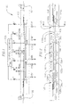
- FIG. 1 is a schematic diagram illustrating a tunable bandpass filter including a microstrip trace pattern and a number of variable capacitors or varactors for tuning the filter in accordance with one embodiment of the present invention.
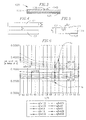
- FIG. 2 is a top view of the microstrip trace pattern of FIG. 1 .
- FIG. 3 is a cross-sectional side view of the microstrip bandpass filter taken along the section 3-3 of FIG. 2 .
- FIG. 4 is a top view of an enlarged portion of a bandpass filter trace pattern, showing overlapped, edge-coupled conductor strips, in accordance with one embodiment of the present invention.
- FIG. 5 is a diagrammatic end view of the bandpass filter of FIG. 4 .
- FIG. 6 is a graph depicting velocities of even and odd modes of propagation as a function of filter parameters, in accordance with one embodiment of the present invention.
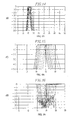
- FIG. 7 is a graph illustrating in a wide band view the performance of the tunable bandpass filter of FIG. 1 at different settings of the filter.
- FIG. 8 is a graph illustrating in a close up view the insertion loss of the tunable bandpass filter of FIG. 1 at different settings of the filter.
- FIG. 9 is a graph illustrating in a close up view the return loss of the tunable bandpass filter of FIG. 1 at different settings of the filter.
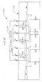
- FIG. 10 is a schematic diagram illustrating a tunable bandpass filter including an alternative microstrip trace pattern and a number of variable capacitors or varactors for tuning the filter in accordance with one embodiment of the present invention.
- FIG. 11 is a perspective view of another embodiment of a bandpass filter including a piezoelectric transducer and a tuning substrate for tuning the filter.
- FIG. 12 is an exploded perspective view of the tunable bandpass filter of FIG. 11 shown from the opposite perspective.
- FIG. 13 is a side view of the tunable bandpass filter of FIG. 11 .
- FIG. 14 is a graph illustrating in a wide band view the performance of the tunable bandpass filter of FIG. 11 at different settings of the filter.
- FIG. 15 is a graph illustrating in a close up view the insertion loss of the tunable bandpass filter of FIG. 11 at different settings of the filter.
- FIG. 16 is a graph illustrating in a close up view the return loss of the tunable bandpass filter of FIG. 11 at different settings of the filter.
- the bandpass filters are tuned by controlling variable capacitors coupled to conductive segments of a conductive trace pattern.
- the conductive segments of the conductive trace pattern are formed in particular shapes designed to compensate for mismatch in the phase velocities for even and odd modes of signal propagation.
- the conductive segments include T-shaped segments and TL-shaped segments arranged in a staggered offset manner. In other embodiments, the conductive segments include only T-shaped segments arranged in the staggered offset manner.
- the bandpass filters are tuned by controlling a piezoelectric transducer coupled to a tuning substrate in close proximity to a conductive trace pattern on a filter substrate. Movement of the tuning substrate in close proximity to the conductive trace pattern changes the effective dielectric constant of the filter substrate, thereby tuning the filter.
- Embodiments of the tunable filters provide good suppression of harmonics, including, for example first, second, third and fourth order harmonics.
- the tunable filters can further provide very low loss, high return loss and a wide tuning range. Such tunable filters have a number of applications.
- an edge coupled filter fabricated in a planar transmission line medium such as a microstrip or stripline transmission line
- energy is propagated through the filter via edge-coupled resonator elements or conductor strips.
- Harmonics in the filter response appear due to the mismatch in phase velocities of the even and odd modes.
- the odd mode travels faster than the even mode.
- the odd mode tends to travel along the outer edges of the microstrip coupled lines or conductor strips, while the even mode tends to travel near the center.
- means for equalizing the even and odd mode electrical lengths and for adjusting the filter pass frequency are provided.
- FIG. 1 is a schematic diagram illustrating a tunable bandpass filter 100 including a microstrip trace pattern 120 and a number of variable capacitors or varactors for tuning the filter in accordance with one embodiment of the present invention.
- the microstrip trace pattern 120 is coupled by capacitors to input/output (I/O) ports 102 and 104.
- FIG. 2 is a top view of the microstrip trace pattern of FIG. 1 .
- the trace pattern 120 includes multiple trace segments or portions (128-140), where each segment is coupled by an inductor (L1-L7), acting as a radio frequency (RF) choke, to bias voltage control circuitry 106.
- the trace segments (128-140) are also coupled by one or more varactor diodes (VD1-VD12) to ground at preselected points along the trace segments.
- the bias voltage control circuitry 106 controls the direct current (DC) bias of each of the trace segments (128-140) of the trace pattern 120. By adjusting the bias voltage at the trace segments (128-140), the filter can be tuned for preselected pass frequencies and preselected ranges.
- the trace pattern 120 includes a series of alternating conductor sections or trace segments (128-140), arranged in a staggered offset manner relative to a filter axis 126.
- the conductor sections are edge-coupled at an RF operating frequency band.
- the spatial separation of the conductor sections provides DC isolation.
- Each trace segment (128-140) includes a coupled line portion which is adjacent to a corresponding coupled line portion of an adjacent conductor section.
- trace segment 132 includes line segment 132a which overlaps with line segment 134a of trace segment 134. In one embodiment, these overlapping line segments are approximately quarter wavelength in length, at an operating frequency.
- the trace pattern 120 includes a first I/O section 122, a second I/O section 124, three T-shaped trace segments (130, 134, 138), four TL-shaped trace segments (128, 132, 136, 140) and the filter axis 126.
- the T-shaped segments and TL-shaped segments each have a primary parallel leg portion oriented along the filter axis, and a transverse stub oriented perpendicular to and bisecting the parallel leg portion.
- the TL-shaped segments further include a secondary parallel leg portion, shorter than the primary parallel leg portion, disposed at the end of the transverse stub opposite to the stub end that bisects the primary parallel leg portion.
- the transverse stub and the secondary parallel leg portion approximately form an L-shape and the transverse stub and the primary parallel section approximately form a T-shape, effectively forming a TL-shape in combination.
- TL-shaped segment 128 includes a primary parallel leg portion, having thin section 128a and thick section 128d along the filter axis 126, a transverse stub 128b and a secondary parallel leg portion 128c.
- the thin section 128a is disposed extremely close to a thin section of the first I/O section 122 for coupling purposes.
- TL-shaped segment 140 includes a primary parallel leg portion, having thin section 140a and thick section 140d along the filter axis 126, a transverse stub 140b and a secondary parallel leg portion 140c.
- the thin section 140a is disposed extremely close to a thin section of the first I/O section 124.
- T-shaped segment 130 includes parallel leg portion 130a and transverse stub portion 130b.
- T-shaped segment 134 includes parallel leg portion 134a and transverse stub portion 134b.
- T-shaped segment 138 includes parallel leg portion 138a and transverse stub portion 138b.
- TL-shaped segment 132 includes primary parallel leg portion 132a, transverse stub 132b, and secondary parallel leg portion 132c.
- TL-shaped segment 136 includes primary parallel leg portion 136a, transverse stub 136b, and secondary parallel leg portion 136c.
- the bias voltage control circuitry 106 controls the DC voltage bias of each T-shaped segment and each TL-shaped segment.
- Each T-shaped segment and each TL-shaped segment is coupled to one or more varactor diodes.
- the varactor diodes modify the capacitance to ground thereby changing the impedance seen by signals traveling along the trace pattern and the frequency response of the tunable filter.
- the impedance of the trace pattern can be defined as including the impedance seen by signals traveling along the trace pattern.
- the characteristics of the frequency response that can be adjusted or tuned include the center frequency along with the overall range of the filter. For example, the center frequency will move up or down as a function of the applied bias voltage.
- the bias voltage control circuitry can be implemented using any combination of processors, memory, discrete logic components, data buses and/or other processing elements that share information.
- a number of jumpers or toggle switches can be used to enable a user to make adjustments to the frequency response characteristics of the filter.
- the filter response can be symmetric about its center frequency (see for example in FIG. 7 ); depending on the length of the quarter wavelength coupled line, the transverse stub lengths may be optimized, which may result in different stub lengths. Since the odd mode tends to travel along the outer edges of the coupled lines or conductor strips, while the even mode tends to travel near the center, the T-shaped and TL-shaped sections add transmission line length which is traveled by the odd mode, but not the even mode. As a result, the odd and even mode components propagating along the trace pattern arrive at the output port in phase. In a number of embodiments, the T-shaped sections or conductor portions are defined as including the TL-shaped sections.
- the filter pattern is symmetric about a line bisecting the filter axis.
- the filter components such as the varactor diodes and inductors, are placed at symmetric locations about the bisecting line.
- the values of such components are matched at symmetric locations about the bisecting line.
- Such symmetry can be important to providing a favorable frequency response.
- other symmetrical configurations can be used.
- non-symmetrical configurations can be used.
- FIG. 3 is a cross-sectional side view of the microstrip bandpass filter 120 taken along the section 3-3 of FIG. 2 .
- the filter embodiments of FIGS. 1, 2 and 3 may be constructed in microstrip. In other embodiments, the tunable filter can be constructed using other suitable materials.
- the filter includes a substantially planar dielectric substrate 123, for example, a substrate such as alumina or duroid having a substrate height h.
- a conductive ground plane layer 125 is formed on one surface of the dielectric substrate, here the bottom surface of the substrate 123.
- the conductive microstrip trace pattern is formed on a opposite substrate surface opposite the ground plane, in this example the top surface (e.g., illustrated portion includes portions of segments 138 and 140).
- the trace pattern forms the conductor sections (128-140) and the I/O ports (122, 124).
- the trace pattern may be fabricated using photo lithographic techniques.
- the trace pattern and ground plane can be implemented using gold, copper or another suitable conductive material.
- the material for the trace pattern and ground plane is selected based on the substrate material.
- the phase velocity mismatches of the even and odd modes may be compensated by extending the odd mode traveling path.
- the alternating T-shaped and TL-shaped portions of the filter provide the compensation.
- the odd mode is faster and tends to travel on the edges of the line, while the even mode is slower and travels along the center of the coupled lines.
- the filter architecture illustrated in FIG. 1 compensates for the mismatch of phase velocities of the even and odd modes in the filter structure by periodically introducing stubs and secondary parallel legs, and by adjusting the electrical length of the quarter wave coupled line sections in the filter.
- most of the phase compensation is provided by the T-shaped or TL-shaped portions. Some phase compensation may be provided by varying the lengths of the coupled lines away from the nominal quarter wavelength, for example, by optimization.
- inductors are used. In other embodiments, more than or less than seven inductors.
- an inductor is coupled to each T-shaped or TL-shaped segment. In other embodiments, an inductor may not be coupled to each segment.
- twelve varactor diodes are coupled to specific areas of the T-shaped and TL-shaped segments. In other embodiments, more than or less than twelve varactor diodes can be coupled at various points along the segments.
- a combination of seven T-shaped and TL-shaped segments are arranged in a staggered offset manner relative to the filter axis.
- more than or less than seven T-shaped and TL-shaped segments can be arranged in different configurations arranged to delay the odd mode propagation for equalizing phase velocity across the tunable filter.
- the varactor diodes can be replaced with other components capable of modifying the capacitance of the trace pattern or segments thereof.
- the varactor diodes can be replaced with other components capable of providing impedance control.
- other suitably shaped segments can be used.
- the filter pattern is symmetric about a line bisecting the filter axis. In such case, the symmetry can be important to a desirable frequency response.
- FIGS. 4, 5, and 6 depict how variations of the design parameters for a microstrip transmission line embodiment affect the phase velocities of the even and odd modes propagating in an edge coupled filter.
- FIG. 4 is a top view of an enlarged portion of a bandpass filter trace pattern, showing overlapped, edge-coupled conductor strips, in accordance with one embodiment of the present invention.
- the filter trace pattern includes edge-coupled conductor strips C1 and C2, having width w, formed as microstrip conductors on a surface of a dielectric substrate 123.
- the conductor strips C 1 and C2 are arranged in parallel, and are spaced apart by a distance s.
- the substrate 123 has a height h.
- FIG. 6 is a graph showing calculated phase velocities for the even mode (ve) and odd mode (vo) as a function of the ratio s/h, and for different ratios w/h.
- FIG. 7 is a graph illustrating in a wide band view the performance of the tunable bandpass filter of FIG. 1 at different settings of the filter.
- a simulation of the tunable filter 120 attenuates the second and third order harmonics as shown in FIG. 7 with very good out-of-band rejection.
- embodiments of the tunable filter even attenuate fourth order harmonics.
- the graph of FIG. 7 further illustrates attenuation as a function of frequency for different settings of an exemplary 15 GHz tunable filter adjusted for eight different passbands centered at frequencies from approximately 14 to 16 GHz.
- the miscellaneous signals seen at 37-41 GHz and 48-50 GHz are below the noise floor.
- the microstrip filters exhibit very low filter loss with very high out-of-band rejection characteristics.
- the microstrip filters exhibit a good linear phase for over 80% of the filter bandwidth, and harmonics in the insertion loss characteristic are effectively suppressed.
- FIG. 8 is a graph illustrating in a close up view the insertion loss of the tunable bandpass filter of FIG. 1 at different settings of the filter. Unlike some conventional filters, the performance characteristics of the illustrated tunable bandpass filter show little degradation from one filter setting to the next.
- FIG. 9 is a graph illustrating in a close up view the return loss of the tunable bandpass filter of FIG. 1 at different settings of the filter.
- FIG. 10 is a schematic diagram illustrating a tunable bandpass filter 200 including an alternative microstrip trace pattern 220 and a number of variable capacitors or varactors (VD1-VD12) for tuning the filter in accordance with one embodiment of the present invention.
- the trace pattern 220 includes multiple trace segments, where each segment is coupled by an inductor (L1-L7), acting as a radio frequency (RF) choke, to a bias voltage control circuitry 206.
- the trace segments are also coupled by one or more varactor diodes (VD1-VD12) to ground.
- the bias voltage control circuitry 206 controls the direct current (DC) bias of the segments of the trace pattern 220. By adjusting the bias voltage at the trace segments, the filter can be tuned for preselected pass frequencies and preselected ranges.
- the structure of the alternative microstrip trace pattern 220 includes similar T-shaped segments/sections arranged in a staggered offset manner relative to a filter axis.
- the conductor sections are edge-coupled at an RF operating frequency band.
- the spatial separation of the conductor sections provides DC isolation.
- the tunable filter of FIG. 10 can operate as described above for the tunable filter of FIG. 1 .
- FIG. 11 is a perspective view of another embodiment of a tunable bandpass filter 300 including a piezoelectric transducer 302 and a tuning substrate 304 for tuning the filter.
- FIG. 12 is an exploded perspective view of the tunable bandpass filter 300 of FIG. 11 from the opposite perspective.
- FIG. 13 is a side view of the tunable bandpass filter 300 of FIG. 11 .
- the tunable filter 300 further includes a filter substrate 306, a filter trace pattern 307, a carrier 308, and a support 310.
- the filter substrate 306 is disposed on a top surface of the carrier 308.
- the filter trace pattern 307 is disposed on a top surface of the filter substrate 306.
- a bottom surface of the support 310 is secured to the top surface of carrier 308.
- a first end of the piezoelectric transducer 304 is attached to a top surface of the support 310.
- a second end of the piezoelectric transducer 304 is attached to the tuning substrate 304.
- a preselected distance h separates the bottom surface of the tuning substrate 304 from the filter trace pattern 307 disposed on the filter substrate 306 (see FIG. 13 ).
- a voltage is applied to the piezoelectric transducer causing up and down movement of the tuning substrate attached to the piezoelectric transducer.
- the movement of the tuning substrate changes the preselected distance h and the effective dielectric constant of the filter trace pattern.
- the filter can be tuned as desired.
- the impedance of the filter trace pattern can be defined as including the impedance seen by signals traveling along the filter trace pattern.
- the piezoelectric transducer is made of lead, zirconate and/or titanate. In other embodiments, the piezoelectric transducer can be made of other suitable materials. For example, in one embodiment, the piezoelectric transducer can be made of any electro-mechanical material where movement of the material can be controlled by a software program.
- the filter trace pattern is extremely similar to the trace pattern of FIGs. 1 and 2 .
- the filter trace pattern of FIG. 10 can be used.
- other suitable trace patterns can be used.
- the tunable filter illustrated in FIGs. 11-13 can provide very good tuning range while effectively eliminating spurious noise.
- FIG. 14 is a graph illustrating in a wide band view the performance of the tunable bandpass filter of FIG. 11 at different settings of the filter.
- a simulation of the tunable filter of FIG. 11 attenuates the second and third order harmonics as shown in FIG. 14 with very good out-of-band rejection.
- embodiments of the tunable filter even attenuate fourth order harmonics.
- the graph of FIG. 14 illustrates attenuation as a function of frequency for different settings of an exemplary 15 GHz tunable filter adjusted for eight passbands centered at frequencies from approximately 14 to 16 GHz.
- the miscellaneous signals seen at 37-41 GHz and 48-50 GHz are below the noise floor.
- the microstrip filters exhibit very low filter loss with very high out-of-band rejection characteristics.
- the microstrip filters exhibit a good linear phase for over 80% of the filter bandwidth, and harmonics in the insertion loss characteristic are effectively suppressed.
- FIG. 15 is a graph illustrating in a close up view the insertion loss of the tunable bandpass filter of FIG. 11 at different settings of the filter. Unlike some conventional filters, the performance characteristics of the illustrated tunable bandpass filter show minimal or non-existent degradation from one filter setting to the next.
- FIG. 16 is a graph illustrating in a close up view the return loss of the tunable bandpass filter of FIG. 11 at different settings of the filter.
- the filter of FIG. 1 has some performance degradation in bandwidth and insertion loss and has a comparatively limited tuning range while effectively eliminating spurious noise.
- the filter of FIG. 11 has very good tuning range with no spurious noise, but the applied voltage required to operate the piezoelectric transducer can be relatively high.
- Each tunable filter can have relative advantages that suit various applications. For example, for the filter illustrated in FIG. 1 , the varactor diode tenability is generally okay, however the tenability range is less than that of the filter of FIG. 11 .
- the tunable filters are very compact, resulting in significant reductions in size and weight as compared to most microwave integrated circuits which utilize multiple filters.
- the filter architecture or trace pattern can be implemented in a transmission line type other than microstrip (e.g., in stripline or coplanar waveguide).
Landscapes
- Physics & Mathematics (AREA)
- Electromagnetism (AREA)
- Control Of Motors That Do Not Use Commutators (AREA)
Abstract
Description
- The present invention relates generally to tunable filters. More specifically, the invention relates to tunable microwave bandpass filters for suppressing spurious signals at harmonics of the pass frequency.
- Most microwave filters built using microstrip transmission lines are not effective at suppressing second, third and fourth harmonic signals. Traditionally, the way to solve this problem is to add a lowpass filter at the two ends of a bandpass filter. Physically, this makes the filter structure undesirably bigger. Electrically, using lowpass filters increases signal loss, and the suppression of the harmonics for the most part is not sufficiently effective.
- Conventional microwave filters that are capable of suppressing such harmonics have been proposed.
U.S. Patent No. 7,145,418 to Akale et al. , the entire content of which is incorporated herein by reference, describes an edge coupled bandpass filter capable of suppressing harmonics. However, some filter applications can require use of different pass frequencies. One way to meet this need is to use a separate filter for each pass frequency. However, the use of multiple filters can be inefficient and expensive. Therefore, a tunable microwave bandpass filter is desirable. - Aspects of the invention relate to a tunable bandpass filter. In one embodiment, the invention relates to a tunable bandpass filter including a dielectric substrate having a first surface opposite to a second surface, a conductive ground plane disposed on the first surface, a microstrip conductive trace pattern disposed on the second surface, the trace pattern defining a phase velocity compensation transmission line section including a series of spaced alternating T-shaped conductor portions, at least one varactor diode coupled to a first T-shaped conductor portion of the series of T-shaped conductor portions and to the conductive ground plane, and bias control circuitry coupled to the first T-shaped conductor portion, wherein the bias control circuitry is configured to control the at least one varactor diode.
- In another embodiment, the invention relates to a tunable bandpass filter including a dielectric substrate having a first surface opposite to a second surface, a conductive ground plane disposed on the first surface, a microstrip conductive trace pattern disposed on the second surface, the trace pattern defining a phase velocity compensation transmission line section including a series of spaced alternating T-shaped conductor portions, a tunable substrate disposed at a preselected distance above the trace pattern, a piezoelectric transducer attached to the tunable substrate, wherein the tunable substrate is configured to move when a voltage is applied to the piezoelectric transducer, wherein a movement of the tunable substrate results in a change to an effective dielectric constant of the filter.
- In yet another embodiment, the invention relates to a tunable bandpass filter including a dielectric substrate having a first surface opposite to a second surface, a conductive ground plane disposed on the first surface, a conductive trace pattern disposed on the second surface, the trace pattern defining a phase velocity compensation transmission line section including a series of spaced alternating T-shaped conductor portions, and a means for adjusting an impedance of the conductive trace pattern.
-
FIG. 1 is a schematic diagram illustrating a tunable bandpass filter including a microstrip trace pattern and a number of variable capacitors or varactors for tuning the filter in accordance with one embodiment of the present invention. -
FIG. 2 is a top view of the microstrip trace pattern ofFIG. 1 . -
FIG. 3 is a cross-sectional side view of the microstrip bandpass filter taken along the section 3-3 ofFIG. 2 . -
FIG. 4 is a top view of an enlarged portion of a bandpass filter trace pattern, showing overlapped, edge-coupled conductor strips, in accordance with one embodiment of the present invention. -
FIG. 5 is a diagrammatic end view of the bandpass filter ofFIG. 4 . -
FIG. 6 is a graph depicting velocities of even and odd modes of propagation as a function of filter parameters, in accordance with one embodiment of the present invention. -
FIG. 7 is a graph illustrating in a wide band view the performance of the tunable bandpass filter ofFIG. 1 at different settings of the filter. -
FIG. 8 is a graph illustrating in a close up view the insertion loss of the tunable bandpass filter ofFIG. 1 at different settings of the filter. -
FIG. 9 is a graph illustrating in a close up view the return loss of the tunable bandpass filter ofFIG. 1 at different settings of the filter. -
FIG. 10 is a schematic diagram illustrating a tunable bandpass filter including an alternative microstrip trace pattern and a number of variable capacitors or varactors for tuning the filter in accordance with one embodiment of the present invention. -
FIG. 11 is a perspective view of another embodiment of a bandpass filter including a piezoelectric transducer and a tuning substrate for tuning the filter. -
FIG. 12 is an exploded perspective view of the tunable bandpass filter ofFIG. 11 shown from the opposite perspective. -
FIG. 13 is a side view of the tunable bandpass filter ofFIG. 11 . -
FIG. 14 is a graph illustrating in a wide band view the performance of the tunable bandpass filter ofFIG. 11 at different settings of the filter. -
FIG. 15 is a graph illustrating in a close up view the insertion loss of the tunable bandpass filter ofFIG. 11 at different settings of the filter. -
FIG. 16 is a graph illustrating in a close up view the return loss of the tunable bandpass filter ofFIG. 11 at different settings of the filter. - Referring now to the drawings, embodiments of tunable bandpass filters are illustrated. In several embodiments, the bandpass filters are tuned by controlling variable capacitors coupled to conductive segments of a conductive trace pattern. The conductive segments of the conductive trace pattern are formed in particular shapes designed to compensate for mismatch in the phase velocities for even and odd modes of signal propagation. In some embodiments, the conductive segments include T-shaped segments and TL-shaped segments arranged in a staggered offset manner. In other embodiments, the conductive segments include only T-shaped segments arranged in the staggered offset manner.
- In some embodiments, the bandpass filters are tuned by controlling a piezoelectric transducer coupled to a tuning substrate in close proximity to a conductive trace pattern on a filter substrate. Movement of the tuning substrate in close proximity to the conductive trace pattern changes the effective dielectric constant of the filter substrate, thereby tuning the filter.
- Embodiments of the tunable filters provide good suppression of harmonics, including, for example first, second, third and fourth order harmonics. The tunable filters can further provide very low loss, high return loss and a wide tuning range. Such tunable filters have a number of applications.
- While not bound by any particular theory, in an edge coupled filter fabricated in a planar transmission line medium, such as a microstrip or stripline transmission line, energy is propagated through the filter via edge-coupled resonator elements or conductor strips. Harmonics in the filter response appear due to the mismatch in phase velocities of the even and odd modes. In microstrip coupled lines, the odd mode travels faster than the even mode. Also, the odd mode tends to travel along the outer edges of the microstrip coupled lines or conductor strips, while the even mode tends to travel near the center. In several embodiments, to suppress the harmonics of the filter, means for equalizing the even and odd mode electrical lengths and for adjusting the filter pass frequency are provided.
-
FIG. 1 is a schematic diagram illustrating atunable bandpass filter 100 including amicrostrip trace pattern 120 and a number of variable capacitors or varactors for tuning the filter in accordance with one embodiment of the present invention. Themicrostrip trace pattern 120 is coupled by capacitors to input/output (I/O)ports -
FIG. 2 is a top view of the microstrip trace pattern ofFIG. 1 . Thetrace pattern 120 includes multiple trace segments or portions (128-140), where each segment is coupled by an inductor (L1-L7), acting as a radio frequency (RF) choke, to biasvoltage control circuitry 106. The trace segments (128-140) are also coupled by one or more varactor diodes (VD1-VD12) to ground at preselected points along the trace segments. The biasvoltage control circuitry 106 controls the direct current (DC) bias of each of the trace segments (128-140) of thetrace pattern 120. By adjusting the bias voltage at the trace segments (128-140), the filter can be tuned for preselected pass frequencies and preselected ranges. - The
trace pattern 120 includes a series of alternating conductor sections or trace segments (128-140), arranged in a staggered offset manner relative to afilter axis 126. The conductor sections are edge-coupled at an RF operating frequency band. The spatial separation of the conductor sections provides DC isolation. Each trace segment (128-140) includes a coupled line portion which is adjacent to a corresponding coupled line portion of an adjacent conductor section. For example, trace segment 132 includesline segment 132a which overlaps withline segment 134a oftrace segment 134. In one embodiment, these overlapping line segments are approximately quarter wavelength in length, at an operating frequency. - In further detail, the
trace pattern 120 includes a first I/O section 122, a second I/O section 124, three T-shaped trace segments (130, 134, 138), four TL-shaped trace segments (128, 132, 136, 140) and thefilter axis 126. The T-shaped segments and TL-shaped segments each have a primary parallel leg portion oriented along the filter axis, and a transverse stub oriented perpendicular to and bisecting the parallel leg portion. The TL-shaped segments further include a secondary parallel leg portion, shorter than the primary parallel leg portion, disposed at the end of the transverse stub opposite to the stub end that bisects the primary parallel leg portion. The transverse stub and the secondary parallel leg portion approximately form an L-shape and the transverse stub and the primary parallel section approximately form a T-shape, effectively forming a TL-shape in combination. - For example, TL-shaped
segment 128 includes a primary parallel leg portion, havingthin section 128a andthick section 128d along thefilter axis 126, atransverse stub 128b and a secondaryparallel leg portion 128c. Thethin section 128a is disposed extremely close to a thin section of the first I/O section 122 for coupling purposes. Similarly, TL-shapedsegment 140 includes a primary parallel leg portion, havingthin section 140a andthick section 140d along thefilter axis 126, atransverse stub 140b and a secondaryparallel leg portion 140c. Thethin section 140a is disposed extremely close to a thin section of the first I/O section 124. - T-shaped segment 130 includes
parallel leg portion 130a andtransverse stub portion 130b. Similarly, T-shapedsegment 134 includesparallel leg portion 134a andtransverse stub portion 134b. Similarly, T-shapedsegment 138 includesparallel leg portion 138a andtransverse stub portion 138b. - TL-shaped segment 132 includes primary
parallel leg portion 132a,transverse stub 132b, and secondary parallel leg portion 132c. Similarly, TL-shapedsegment 136 includes primaryparallel leg portion 136a,transverse stub 136b, and secondaryparallel leg portion 136c. - The bias
voltage control circuitry 106 controls the DC voltage bias of each T-shaped segment and each TL-shaped segment. Each T-shaped segment and each TL-shaped segment is coupled to one or more varactor diodes. By changing the DC bias at each segment, the varactor diodes modify the capacitance to ground thereby changing the impedance seen by signals traveling along the trace pattern and the frequency response of the tunable filter. In some circumstances, the impedance of the trace pattern can be defined as including the impedance seen by signals traveling along the trace pattern. The characteristics of the frequency response that can be adjusted or tuned include the center frequency along with the overall range of the filter. For example, the center frequency will move up or down as a function of the applied bias voltage. - The bias voltage control circuitry can be implemented using any combination of processors, memory, discrete logic components, data buses and/or other processing elements that share information. In some embodiments, a number of jumpers or toggle switches can be used to enable a user to make adjustments to the frequency response characteristics of the filter.
- The filter response can be symmetric about its center frequency (see for example in
FIG. 7 ); depending on the length of the quarter wavelength coupled line, the transverse stub lengths may be optimized, which may result in different stub lengths. Since the odd mode tends to travel along the outer edges of the coupled lines or conductor strips, while the even mode tends to travel near the center, the T-shaped and TL-shaped sections add transmission line length which is traveled by the odd mode, but not the even mode. As a result, the odd and even mode components propagating along the trace pattern arrive at the output port in phase. In a number of embodiments, the T-shaped sections or conductor portions are defined as including the TL-shaped sections. - In the filter embodiments illustrated in
FIG. 1 and FIG. 2 , the filter pattern is symmetric about a line bisecting the filter axis. In addition, the filter components, such as the varactor diodes and inductors, are placed at symmetric locations about the bisecting line. In some embodiments, the values of such components are matched at symmetric locations about the bisecting line. Such symmetry can be important to providing a favorable frequency response. In other embodiments, other symmetrical configurations can be used. In some embodiments, non-symmetrical configurations can be used. -
FIG. 3 is a cross-sectional side view of themicrostrip bandpass filter 120 taken along the section 3-3 ofFIG. 2 . The filter embodiments ofFIGS. 1, 2 and3 may be constructed in microstrip. In other embodiments, the tunable filter can be constructed using other suitable materials. The filter includes a substantially planardielectric substrate 123, for example, a substrate such as alumina or duroid having a substrate height h. A conductiveground plane layer 125 is formed on one surface of the dielectric substrate, here the bottom surface of thesubstrate 123. The conductive microstrip trace pattern is formed on a opposite substrate surface opposite the ground plane, in this example the top surface (e.g., illustrated portion includes portions ofsegments 138 and 140). The trace pattern forms the conductor sections (128-140) and the I/O ports (122, 124). In one embodiment, the trace pattern may be fabricated using photo lithographic techniques. In several embodiments, the trace pattern and ground plane can be implemented using gold, copper or another suitable conductive material. In some embodiments, the material for the trace pattern and ground plane is selected based on the substrate material. - The phase velocity mismatches of the even and odd modes may be compensated by extending the odd mode traveling path. In one embodiment of the filter structure, the alternating T-shaped and TL-shaped portions of the filter provide the compensation. In a microstrip coupled line, the odd mode is faster and tends to travel on the edges of the line, while the even mode is slower and travels along the center of the coupled lines. The filter architecture illustrated in
FIG. 1 compensates for the mismatch of phase velocities of the even and odd modes in the filter structure by periodically introducing stubs and secondary parallel legs, and by adjusting the electrical length of the quarter wave coupled line sections in the filter. In several embodiments, most of the phase compensation is provided by the T-shaped or TL-shaped portions. Some phase compensation may be provided by varying the lengths of the coupled lines away from the nominal quarter wavelength, for example, by optimization. - In the embodiment illustrated in
FIG. 1 , seven inductors are used. In other embodiments, more than or less than seven inductors. In the embodiment illustrated inFIG. 1 , an inductor is coupled to each T-shaped or TL-shaped segment. In other embodiments, an inductor may not be coupled to each segment. In the embodiment illustrated inFIG. 1 , twelve varactor diodes are coupled to specific areas of the T-shaped and TL-shaped segments. In other embodiments, more than or less than twelve varactor diodes can be coupled at various points along the segments. - In the embodiment illustrated in
FIG. 1 , a combination of seven T-shaped and TL-shaped segments are arranged in a staggered offset manner relative to the filter axis. In other embodiments, more than or less than seven T-shaped and TL-shaped segments can be arranged in different configurations arranged to delay the odd mode propagation for equalizing phase velocity across the tunable filter. In other embodiments, the varactor diodes can be replaced with other components capable of modifying the capacitance of the trace pattern or segments thereof. In some embodiments, the varactor diodes can be replaced with other components capable of providing impedance control. In other embodiments, other suitably shaped segments can be used. In a number of embodiments, the filter pattern is symmetric about a line bisecting the filter axis. In such case, the symmetry can be important to a desirable frequency response. -
FIGS. 4, 5, and 6 depict how variations of the design parameters for a microstrip transmission line embodiment affect the phase velocities of the even and odd modes propagating in an edge coupled filter.FIG. 4 is a top view of an enlarged portion of a bandpass filter trace pattern, showing overlapped, edge-coupled conductor strips, in accordance with one embodiment of the present invention. The filter trace pattern includes edge-coupled conductor strips C1 and C2, having width w, formed as microstrip conductors on a surface of adielectric substrate 123. The conductor stripsC 1 and C2 are arranged in parallel, and are spaced apart by a distance s. As depicted in the end view,FIG. 5 , thesubstrate 123 has a height h.FIG. 6 is a graph showing calculated phase velocities for the even mode (ve) and odd mode (vo) as a function of the ratio s/h, and for different ratios w/h. -
FIG. 7 is a graph illustrating in a wide band view the performance of the tunable bandpass filter ofFIG. 1 at different settings of the filter. In several embodiments, a simulation of thetunable filter 120 attenuates the second and third order harmonics as shown inFIG. 7 with very good out-of-band rejection. In some circumstances, embodiments of the tunable filter even attenuate fourth order harmonics. The graph ofFIG. 7 further illustrates attenuation as a function of frequency for different settings of an exemplary 15 GHz tunable filter adjusted for eight different passbands centered at frequencies from approximately 14 to 16 GHz. In the graph illustrated inFIG. 7 , there are effectively no spurious signals up to 50 GHz. The miscellaneous signals seen at 37-41 GHz and 48-50 GHz are below the noise floor. - In several embodiments, the microstrip filters exhibit very low filter loss with very high out-of-band rejection characteristics. In a number of embodiments, the microstrip filters exhibit a good linear phase for over 80% of the filter bandwidth, and harmonics in the insertion loss characteristic are effectively suppressed.
-
FIG. 8 is a graph illustrating in a close up view the insertion loss of the tunable bandpass filter ofFIG. 1 at different settings of the filter. Unlike some conventional filters, the performance characteristics of the illustrated tunable bandpass filter show little degradation from one filter setting to the next. -
FIG. 9 is a graph illustrating in a close up view the return loss of the tunable bandpass filter ofFIG. 1 at different settings of the filter. -
FIG. 10 is a schematic diagram illustrating atunable bandpass filter 200 including an alternativemicrostrip trace pattern 220 and a number of variable capacitors or varactors (VD1-VD12) for tuning the filter in accordance with one embodiment of the present invention. - The
trace pattern 220 includes multiple trace segments, where each segment is coupled by an inductor (L1-L7), acting as a radio frequency (RF) choke, to a biasvoltage control circuitry 206. The trace segments are also coupled by one or more varactor diodes (VD1-VD12) to ground. The biasvoltage control circuitry 206 controls the direct current (DC) bias of the segments of thetrace pattern 220. By adjusting the bias voltage at the trace segments, the filter can be tuned for preselected pass frequencies and preselected ranges. - As compared to the tunable filter of
FIG. 1 , the structure of the alternativemicrostrip trace pattern 220 includes similar T-shaped segments/sections arranged in a staggered offset manner relative to a filter axis. The conductor sections are edge-coupled at an RF operating frequency band. The spatial separation of the conductor sections provides DC isolation. - However, in the embodiment illustrated in
FIG. 10 , only T-shaped sections are arranged in the staggered offset manner. This microstrip trace pattern can provide sufficient performance characteristics for a number of applications. However, in a number of embodiments, the performance characteristics, such as range of frequency response and range of tunability, of the tunable filter ofFIG. 1 are superior to those of the tunable filter ofFIG. 10 , In some applications, however, the tunable filter ofFIG. 10 can be preferred. - In a number of aspects, the tunable filter of
FIG. 10 can operate as described above for the tunable filter ofFIG. 1 . -
FIG. 11 is a perspective view of another embodiment of atunable bandpass filter 300 including apiezoelectric transducer 302 and atuning substrate 304 for tuning the filter.FIG. 12 is an exploded perspective view of thetunable bandpass filter 300 ofFIG. 11 from the opposite perspective.FIG. 13 is a side view of thetunable bandpass filter 300 ofFIG. 11 . Thetunable filter 300 further includes afilter substrate 306, afilter trace pattern 307, acarrier 308, and asupport 310. Thefilter substrate 306 is disposed on a top surface of thecarrier 308. Thefilter trace pattern 307 is disposed on a top surface of thefilter substrate 306. A bottom surface of thesupport 310 is secured to the top surface ofcarrier 308. A first end of thepiezoelectric transducer 304 is attached to a top surface of thesupport 310. A second end of thepiezoelectric transducer 304 is attached to thetuning substrate 304. A preselected distance h separates the bottom surface of thetuning substrate 304 from thefilter trace pattern 307 disposed on the filter substrate 306 (seeFIG. 13 ). - In operation, a voltage is applied to the piezoelectric transducer causing up and down movement of the tuning substrate attached to the piezoelectric transducer. The movement of the tuning substrate changes the preselected distance h and the effective dielectric constant of the filter trace pattern. By controlling the effective dielectric constant or impedance seen by signals traveling along the filter trace pattern, the filter can be tuned as desired. In some circumstances, the impedance of the filter trace pattern can be defined as including the impedance seen by signals traveling along the filter trace pattern.
- In one embodiment, the piezoelectric transducer is made of lead, zirconate and/or titanate. In other embodiments, the piezoelectric transducer can be made of other suitable materials. For example, in one embodiment, the piezoelectric transducer can be made of any electro-mechanical material where movement of the material can be controlled by a software program.
- In the embodiment illustrated in
FIGs. 11 and 12 , the filter trace pattern is extremely similar to the trace pattern ofFIGs. 1 and 2 . In another embodiment, the filter trace pattern ofFIG. 10 can be used. In other embodiments, other suitable trace patterns can be used. - As for performance, the tunable filter illustrated in
FIGs. 11-13 can provide very good tuning range while effectively eliminating spurious noise. -
FIG. 14 is a graph illustrating in a wide band view the performance of the tunable bandpass filter ofFIG. 11 at different settings of the filter. In several embodiments, a simulation of the tunable filter ofFIG. 11 attenuates the second and third order harmonics as shown inFIG. 14 with very good out-of-band rejection. In some circumstances, embodiments of the tunable filter even attenuate fourth order harmonics. The graph ofFIG. 14 illustrates attenuation as a function of frequency for different settings of an exemplary 15 GHz tunable filter adjusted for eight passbands centered at frequencies from approximately 14 to 16 GHz. In the graph illustrated inFIG. 14 , there are effectively no spurious signals up to 50 GHz. The miscellaneous signals seen at 37-41 GHz and 48-50 GHz are below the noise floor. - In several embodiments, the microstrip filters exhibit very low filter loss with very high out-of-band rejection characteristics. In a number of embodiments, the microstrip filters exhibit a good linear phase for over 80% of the filter bandwidth, and harmonics in the insertion loss characteristic are effectively suppressed.
-
FIG. 15 is a graph illustrating in a close up view the insertion loss of the tunable bandpass filter ofFIG. 11 at different settings of the filter. Unlike some conventional filters, the performance characteristics of the illustrated tunable bandpass filter show minimal or non-existent degradation from one filter setting to the next. -
FIG. 16 is a graph illustrating in a close up view the return loss of the tunable bandpass filter ofFIG. 11 at different settings of the filter. - In comparing the tunable filters of
FIG. 1 andFIG. 11 , the filter ofFIG. 1 has some performance degradation in bandwidth and insertion loss and has a comparatively limited tuning range while effectively eliminating spurious noise. On the other hand, the filter ofFIG. 11 has very good tuning range with no spurious noise, but the applied voltage required to operate the piezoelectric transducer can be relatively high. Each tunable filter can have relative advantages that suit various applications. For example, for the filter illustrated inFIG. 1 , the varactor diode tenability is generally okay, however the tenability range is less than that of the filter ofFIG. 11 . - In many embodiments, the tunable filters are very compact, resulting in significant reductions in size and weight as compared to most microwave integrated circuits which utilize multiple filters. In some embodiments, the filter architecture or trace pattern can be implemented in a transmission line type other than microstrip (e.g., in stripline or coplanar waveguide).
- While the above description contains many specific embodiments of the invention, these should not be construed as limitations on the scope of the invention, but rather as examples of specific embodiments thereof. Accordingly, the scope of the invention should be determined not by the embodiments illustrated, but by the appended claims and their equivalents.
Claims (18)
- A tunable bandpass filter comprising:a dielectric substrate having a first surface opposite to a second surface;a conductive ground plane disposed on the first surface;a conductive trace pattern disposed on the second surface, the trace pattern defining a phase velocity compensation transmission line section comprising a series of spaced alternating T-shaped conductor portions; anda means for adjusting an impedance of the conductive trace pattern.
- A tunable bandpass filter as claimed in claim 1, wherein the means for adjusting comprises:at least one varactor diode coupled to a first T-shaped conductor portion of the series of T-shaped conductor portions and to the conductive ground plane; andbias control circuitry coupled to the first T-shaped conductor portion, wherein the bias control circuitry is configured to control the at least one varactor diode.
- The tunable bandpass filter of claim 2:wherein the T-shaped conductor portions comprise a parallel leg and a transverse stub, the transverse stub providing a transmission line length traveled by an odd mode of energy propagation and not by an even mode of energy propagation; andwherein the phase velocity compensation transmission line section provides phase compensation for odd mode energy propagation at a different rate than even mode energy propagation.
- The tunable bandpass filter of claim 2, further comprising:a first varactor diode coupled to the first T-shaped conductor portion of the T-shaped conductor portions and to the conductive ground plane;a second varactor diode coupled to a second T-shaped conductor portion of the T-shaped conductor portions and to the conductive ground plane; andthe bias control circuitry coupled to the first T-shaped conductor portion and the second T-shaped conductor portion;
wherein the bias control circuitry is configured to control a voltage provided to the first varactor diode and the second varactor diode. - The tunable bandpass filter of claim 2, further comprising:a first varactor diode coupled to the first T-shaped conductor portion of the T-shaped conductor portions and to the conductive ground plane;a second varactor diode coupled to the first T-shaped conductor portion of the T-shaped conductor portions and to the conductive ground plane; andthe bias control circuitry coupled to the first T-shaped conductor portion;wherein the bias control circuitry is configured to control a voltage provided to the first varactor diode and the second varactor diode.
- The tunable bandpass filter of claim 2, further comprising a first inductor coupled in series between the first T-shaped conductor portion and the bias control circuitry.
- The tunable bandpass filter of claim 2, wherein the bias control circuitry is configured to change a frequency response of the filter by controlling the at least one varactor diode.
- A tunable bandpass filter as claimed in claim 1, wherein the means for adjusting comprises:a tunable substrate disposed at a preselected distance above the trace pattern;a piezoelectric transducer attached to the tunable substrate;wherein the tunable substrate is configured to move when a voltage is applied to the piezoelectric transducer;wherein a movement of the tunable substrate results in a change to an effective dielectric constant of the filter.
- The tunable bandpass filter of claim 8, further comprising:a support attached to the piezoelectric transducer; anda carrier having a top surface;wherein the dielectric substrate is disposed on the top surface of the carrier; andwherein the support is disposed on the top surface of the carrier.
- The tunable bandpass filter of claim 9:wherein the carrier comprises a first end opposite to a second end;wherein the dielectric substrate is disposed on the top surface at the first end of the carrier; andwherein the support is disposed on the top surface at the second end of the carrier.
- The tunable bandpass filter of claim 8:wherein a movement of the tunable substrate results in a change in the preselected distance between the tuning substrate and the trace pattern.
- The tunable bandpass filter of claim 8:wherein the T-shaped conductor portions comprise a parallel leg and a transverse stub, the transverse stub providing a transmission line length traveled by an odd mode of energy propagation and not by an even mode of energy propagation; andwherein the phase velocity compensation transmission line section provides phase compensation for odd mode energy propagation at a different rate than even mode energy propagation.
- The tunable bandpass filter of claim 2 or claim 8, wherein the phase velocity compensation transmission line section provides suppression of at least second and third order harmonics of a filter response.
- The tunable bandpass filter of claim 2 or claim 8, wherein the series of T-shaped conductor portions comprise at least one TL-shaped conductor portion, wherein the at least one TL-shaped conductor portion comprises:a primary parallel leg oriented parallel to a filter axis;a transverse stub having a first end coupled to the primary parallel leg; anda secondary parallel leg coupled to the transverse stub, the secondary parallel leg oriented parallel to the filter axis;wherein the transverse stub and secondary parallel leg are arranged to provide a transmission line length traveled by an odd mode of energy propagation and not by an even mode of energy propagation; andwherein the phase velocity compensation transmission line section provides phase compensation for odd mode energy propagation at a different rate than even mode energy propagation.
- The tunable bandpass filter of claim 2 or claim 8, wherein the T-shaped conductor portions comprise:a parallel leg oriented parallel to a filter axis;a transverse stub having a first end coupled to the primary parallel leg, the transverse stub oriented perpendicular to the filter axis;wherein the transverse stub provides a transmission line length traveled by an odd mode of energy propagation and not by an even mode of energy propagation; andwherein the phase velocity compensation transmission line section provides phase compensation for odd mode energy propagation at a different rate than even mode energy propagation.
- The tunable bandpass filter of claim 15, wherein the transverse stub of the T-shaped portion bisects the parallel leg.
- The tunable bandpass filter of claim 2 or claim 8, further comprising:a first input/output port at one end of the trace pattern;a second input/output port at an opposite end of the trace pattern;a filter axis line extending from the first port to the second port; anda dividing axis bisecting the filter axis line;wherein the trace pattern is symmetric about the dividing axis.
- The tunable bandpass filter of claim 2 or claim 8, wherein the conductive trace pattern comprises a microstrip conductive trace pattern.
Applications Claiming Priority (1)
| Application Number | Priority Date | Filing Date | Title |
|---|---|---|---|
| US12/469,620 US20100295634A1 (en) | 2009-05-20 | 2009-05-20 | Tunable bandpass filter |
Publications (1)
| Publication Number | Publication Date |
|---|---|
| EP2254195A1 true EP2254195A1 (en) | 2010-11-24 |
Family
ID=42320660
Family Applications (1)
| Application Number | Title | Priority Date | Filing Date |
|---|---|---|---|
| EP10250906A Withdrawn EP2254195A1 (en) | 2009-05-20 | 2010-05-11 | Tunable bandpass filter |
Country Status (3)
| Country | Link |
|---|---|
| US (3) | US20100295634A1 (en) |
| EP (1) | EP2254195A1 (en) |
| IL (1) | IL204691A (en) |
Cited By (8)
| Publication number | Priority date | Publication date | Assignee | Title |
|---|---|---|---|---|
| CN102610888A (en) * | 2012-02-27 | 2012-07-25 | 浙江纺织服装职业技术学院 | Radio frequency filter capable of automatically sensing and rapidly regulating frequency and bandwidth |
| EP3203641A1 (en) | 2016-02-08 | 2017-08-09 | Bayerische Motoren Werke Aktiengesellschaft | A filter and a method for isolating terminals in a transceiver front end |
| EP3203640A1 (en) | 2016-02-08 | 2017-08-09 | Bayerische Motoren Werke Aktiengesellschaft | A filter and a method for filtering an analog radio-frequency input signal |
| CN109687067A (en) * | 2019-01-07 | 2019-04-26 | 西南交通大学 | A kind of coupled structure for full variable band-pass filter |
| WO2019232673A1 (en) * | 2018-06-04 | 2019-12-12 | Nokia Shanghai Bell Co., Ltd. | A cavity filter |
| CN110729533A (en) * | 2019-09-30 | 2020-01-24 | 西南电子技术研究所(中国电子科技集团公司第十研究所) | Asymmetric SIR Loaded Broadband Suppression Broadband Bandpass Filter |
| CN112332054A (en) * | 2020-11-18 | 2021-02-05 | 辽宁工程技术大学 | Dual-passband band-pass filter based on asymmetric coupling line |
| US12040523B2 (en) | 2019-04-04 | 2024-07-16 | Nokia Solutions And Networks Oy | Resonator and filter |
Families Citing this family (8)
| Publication number | Priority date | Publication date | Assignee | Title |
|---|---|---|---|---|
| US7583950B2 (en) * | 2006-10-05 | 2009-09-01 | Harris Corporation | High linearity tunable bandpass filter |
| JP4852088B2 (en) * | 2008-11-04 | 2012-01-11 | 株式会社東芝 | Bias circuit |
| US9225051B2 (en) * | 2010-09-28 | 2015-12-29 | The Goverment of the United States of America, as represented by the Secretary of the Navy | Tuning bandwidth and center frequencies in a bandpass filter |
| JP2012191521A (en) * | 2011-03-11 | 2012-10-04 | Fujitsu Ltd | Variable filter device and communication device |
| WO2012161676A1 (en) * | 2011-05-20 | 2012-11-29 | Trilithic, Inc. | Voltage tunable filters |
| DE202011105662U1 (en) * | 2011-09-14 | 2012-05-09 | IAD Gesellschaft für Informatik, Automatisierung und Datenverarbeitung mbH | Reconfigurable bandpass filter based on planar comb filters with varactor diodes |
| US10181840B1 (en) | 2014-08-21 | 2019-01-15 | National Technology & Engineering Solutions Of Sandia, Llc | Gm-C filter and multi-phase clock circuit |
| CN113451728B (en) * | 2021-05-31 | 2022-06-14 | 西南电子技术研究所(中国电子科技集团公司第十研究所) | Miniaturized T-shaped dual-mode resonator |
Citations (6)
| Publication number | Priority date | Publication date | Assignee | Title |
|---|---|---|---|---|
| EP0371446A2 (en) * | 1988-11-28 | 1990-06-06 | Fujitsu Limited | Band pass filter |
| WO2000055936A1 (en) * | 1999-03-16 | 2000-09-21 | Superconductor Technologies, Inc. | High temperature superconductor tunable filter |
| US6323745B1 (en) * | 1999-09-09 | 2001-11-27 | Qualcomm Inc. | Planar bandpass filter |
| US6525630B1 (en) * | 1999-11-04 | 2003-02-25 | Paratek Microwave, Inc. | Microstrip tunable filters tuned by dielectric varactors |
| WO2003028146A1 (en) * | 2001-09-27 | 2003-04-03 | Qualcomm Incorporated | Electrically tunable bandpass filters |
| US20060125578A1 (en) * | 2004-12-15 | 2006-06-15 | Tamrat Akale | Bandpass filter |
Family Cites Families (17)
| Publication number | Priority date | Publication date | Assignee | Title |
|---|---|---|---|---|
| US3104362A (en) * | 1959-08-27 | 1963-09-17 | Thompson Ramo Wooldridge Inc | Microwave filter |
| US3343069A (en) * | 1963-12-19 | 1967-09-19 | Hughes Aircraft Co | Parametric frequency doubler-limiter |
| US3646413A (en) * | 1970-09-25 | 1972-02-29 | Avco Corp | Piezoelectric-driven variable capacitor |
| US4020429A (en) * | 1976-02-12 | 1977-04-26 | Motorola, Inc. | High power radio frequency tunable circuits |
| JPH02152302A (en) * | 1988-12-02 | 1990-06-12 | Fujitsu Ltd | Double wave blocking circuit |
| GB2247125B (en) * | 1990-08-16 | 1995-01-11 | Technophone Ltd | Tunable bandpass filter |
| US5406233A (en) * | 1991-02-08 | 1995-04-11 | Massachusetts Institute Of Technology | Tunable stripline devices |
| US5442330A (en) * | 1993-12-27 | 1995-08-15 | Motorola, Inc. | Coupled line filter with improved out-of-band rejection |
| US6252476B1 (en) * | 2000-04-19 | 2001-06-26 | Rockwell Collins, Inc. | Microstrip resonators and coupled line bandpass filters using same |
| US6778042B2 (en) * | 2000-10-30 | 2004-08-17 | Kabushiki Kaisha Toshiba | High-frequency device |
| WO2002099923A1 (en) * | 2001-04-17 | 2002-12-12 | Paratek Microwave, Inc. | Hairpin microstrip line electrically tunable filters |
| US6784766B2 (en) * | 2002-08-21 | 2004-08-31 | Raytheon Company | MEMS tunable filters |
| US7085121B2 (en) * | 2002-10-21 | 2006-08-01 | Hrl Laboratories, Llc | Variable capacitance membrane actuator for wide band tuning of microstrip resonators and filters |
| US7656071B2 (en) * | 2002-10-21 | 2010-02-02 | Hrl Laboratories, Llc | Piezoelectric actuator for tunable electronic components |
| US7057481B2 (en) * | 2004-03-09 | 2006-06-06 | Alpha Networks Inc. | PCB based band-pass filter for cutting out harmonic high frequency |
| DE112004002785B4 (en) * | 2004-05-31 | 2014-03-13 | Fujitsu Ltd. | Variable capacitor and manufacturing method thereof |
| US7372373B2 (en) * | 2004-08-27 | 2008-05-13 | Itron, Inc. | Embedded antenna and filter apparatus and methodology |
-
2009
- 2009-05-20 US US12/469,620 patent/US20100295634A1/en not_active Abandoned
-
2010
- 2010-03-23 IL IL204691A patent/IL204691A/en active IP Right Grant
- 2010-05-11 EP EP10250906A patent/EP2254195A1/en not_active Withdrawn
-
2011
- 2011-09-07 US US13/227,422 patent/US8242862B2/en active Active
-
2012
- 2012-07-10 US US13/545,923 patent/US8760243B2/en active Active
Patent Citations (7)
| Publication number | Priority date | Publication date | Assignee | Title |
|---|---|---|---|---|
| EP0371446A2 (en) * | 1988-11-28 | 1990-06-06 | Fujitsu Limited | Band pass filter |
| WO2000055936A1 (en) * | 1999-03-16 | 2000-09-21 | Superconductor Technologies, Inc. | High temperature superconductor tunable filter |
| US6323745B1 (en) * | 1999-09-09 | 2001-11-27 | Qualcomm Inc. | Planar bandpass filter |
| US6525630B1 (en) * | 1999-11-04 | 2003-02-25 | Paratek Microwave, Inc. | Microstrip tunable filters tuned by dielectric varactors |
| WO2003028146A1 (en) * | 2001-09-27 | 2003-04-03 | Qualcomm Incorporated | Electrically tunable bandpass filters |
| US20060125578A1 (en) * | 2004-12-15 | 2006-06-15 | Tamrat Akale | Bandpass filter |
| US7145418B2 (en) | 2004-12-15 | 2006-12-05 | Raytheon Company | Bandpass filter |
Non-Patent Citations (1)
| Title |
|---|
| MASOUD KOOCHAKZADEH ET AL: "Tunable Filters With Nonuniform Microstrip Coupled Lines", IEEE MICROWAVE AND WIRELESS COMPONENTS LETTERS, IEEE SERVICE CENTER, NEW YORK, NY, US, vol. 17, no. 5, 1 May 2008 (2008-05-01), pages 314 - 316, XP011208248, ISSN: 1531-1309 * |
Cited By (12)
| Publication number | Priority date | Publication date | Assignee | Title |
|---|---|---|---|---|
| CN102610888A (en) * | 2012-02-27 | 2012-07-25 | 浙江纺织服装职业技术学院 | Radio frequency filter capable of automatically sensing and rapidly regulating frequency and bandwidth |
| CN102610888B (en) * | 2012-02-27 | 2014-03-05 | 浙江纺织服装职业技术学院 | An RF filter that automatically senses and quickly adjusts frequency and bandwidth |
| EP3203641A1 (en) | 2016-02-08 | 2017-08-09 | Bayerische Motoren Werke Aktiengesellschaft | A filter and a method for isolating terminals in a transceiver front end |
| EP3203640A1 (en) | 2016-02-08 | 2017-08-09 | Bayerische Motoren Werke Aktiengesellschaft | A filter and a method for filtering an analog radio-frequency input signal |
| WO2017137891A1 (en) | 2016-02-08 | 2017-08-17 | Bayerische Motoren Werke Aktiengesellschaft | A cascade of filters and a method for filtering an analog radio-frequency input signal |
| US11469791B2 (en) | 2016-02-08 | 2022-10-11 | Bayerische Motoren Werke Aktiengesellschaft | Cascade of filters and a method for filtering an analog radio-frequency input signal |
| WO2019232673A1 (en) * | 2018-06-04 | 2019-12-12 | Nokia Shanghai Bell Co., Ltd. | A cavity filter |
| CN109687067A (en) * | 2019-01-07 | 2019-04-26 | 西南交通大学 | A kind of coupled structure for full variable band-pass filter |
| US12040523B2 (en) | 2019-04-04 | 2024-07-16 | Nokia Solutions And Networks Oy | Resonator and filter |
| CN110729533A (en) * | 2019-09-30 | 2020-01-24 | 西南电子技术研究所(中国电子科技集团公司第十研究所) | Asymmetric SIR Loaded Broadband Suppression Broadband Bandpass Filter |
| CN110729533B (en) * | 2019-09-30 | 2021-02-09 | 西南电子技术研究所(中国电子科技集团公司第十研究所) | Asymmetric SIR loaded wide stop band suppression broadband band-pass filter |
| CN112332054A (en) * | 2020-11-18 | 2021-02-05 | 辽宁工程技术大学 | Dual-passband band-pass filter based on asymmetric coupling line |
Also Published As
| Publication number | Publication date |
|---|---|
| US20110316653A1 (en) | 2011-12-29 |
| IL204691A (en) | 2014-08-31 |
| US20100295634A1 (en) | 2010-11-25 |
| US8760243B2 (en) | 2014-06-24 |
| US20120274422A1 (en) | 2012-11-01 |
| US8242862B2 (en) | 2012-08-14 |
| IL204691A0 (en) | 2010-11-30 |
Similar Documents
| Publication | Publication Date | Title |
|---|---|---|
| US8242862B2 (en) | Tunable bandpass filter | |
| US9270008B2 (en) | Transmission line resonator, bandpass filter using transmission line resonator, multiplexer, balanced-to-unbalanced transformer, power divider, unbalanced-to-balanced transformer, frequency mixer, and balance-type filter | |
| US8797126B2 (en) | Tunable microwave arrangements | |
| US6577211B1 (en) | Transmission line, filter, duplexer and communication device | |
| US5343176A (en) | Radio frequency filter having a substrate with recessed areas | |
| KR100892024B1 (en) | Bandpass filter | |
| JP2007013962A (en) | Multilayer bandpass filter | |
| US20110215886A1 (en) | Multirole circuit element capable of operating as variable resonator or transmission line and variable filter incorporating the same | |
| US6323745B1 (en) | Planar bandpass filter | |
| US20160211563A1 (en) | Structure and electronic circuit | |
| EP1034576B1 (en) | Multi surface coupled coaxial resonator | |
| JPH0443703A (en) | Symmetrical strip line resonator | |
| Jones et al. | Miniaturized reconfigurable dual-band bandstop filter with independent stopband control using folded ridged quarter-mode substrate integrated waveguide | |
| US20050107060A1 (en) | Stripline filter utilizing one or more inter-resonator coupling means | |
| JP4251974B2 (en) | High frequency filter | |
| US9474150B2 (en) | Transmission line filter with tunable capacitor | |
| KR101250060B1 (en) | Electrically tunable bandpass filters | |
| US12431601B2 (en) | Printed microstrip filter | |
| US11322813B2 (en) | Band pass filter, communication device, and resonator | |
| US11228077B2 (en) | Microstrip DC block | |
| CN110994114B (en) | A controllable passband dual-mode filter based on a compact dielectric resonator | |
| del Castillo Velazquez-Ahumada et al. | Design of a dual band-pass filter using modified folded stepped-impedance resonators | |
| US20230143899A1 (en) | Filter | |
| US11962055B2 (en) | Waveguide band-stop filter arrangement | |
| CN121790709A (en) | Compact broadband band-pass filter adopting parallel coupling line structure |
Legal Events
| Date | Code | Title | Description |
|---|---|---|---|
| PUAI | Public reference made under article 153(3) epc to a published international application that has entered the european phase |
Free format text: ORIGINAL CODE: 0009012 |
|
| AK | Designated contracting states |
Kind code of ref document: A1 Designated state(s): AL AT BE BG CH CY CZ DE DK EE ES FI FR GB GR HR HU IE IS IT LI LT LU LV MC MK MT NL NO PL PT RO SE SI SK SM TR |
|
| AX | Request for extension of the european patent |
Extension state: BA ME RS |
|
| 17P | Request for examination filed |
Effective date: 20110524 |
|
| 17Q | First examination report despatched |
Effective date: 20120308 |
|
| GRAP | Despatch of communication of intention to grant a patent |
Free format text: ORIGINAL CODE: EPIDOSNIGR1 |
|
| INTG | Intention to grant announced |
Effective date: 20180404 |
|
| STAA | Information on the status of an ep patent application or granted ep patent |
Free format text: STATUS: THE APPLICATION IS DEEMED TO BE WITHDRAWN |
|
| 18D | Application deemed to be withdrawn |
Effective date: 20180815 |