EP2251905A2 - Solid-state imaging device, electronic apparatus, and method for manufacturing solid-state imaging device - Google Patents
Solid-state imaging device, electronic apparatus, and method for manufacturing solid-state imaging device Download PDFInfo
- Publication number
- EP2251905A2 EP2251905A2 EP10004648A EP10004648A EP2251905A2 EP 2251905 A2 EP2251905 A2 EP 2251905A2 EP 10004648 A EP10004648 A EP 10004648A EP 10004648 A EP10004648 A EP 10004648A EP 2251905 A2 EP2251905 A2 EP 2251905A2
- Authority
- EP
- European Patent Office
- Prior art keywords
- wiring
- wiring layer
- state imaging
- imaging device
- layer
- Prior art date
- Legal status (The legal status is an assumption and is not a legal conclusion. Google has not performed a legal analysis and makes no representation as to the accuracy of the status listed.)
- Ceased
Links
Images











Classifications
-
- H—ELECTRICITY
- H10—SEMICONDUCTOR DEVICES; ELECTRIC SOLID-STATE DEVICES NOT OTHERWISE PROVIDED FOR
- H10F—INORGANIC SEMICONDUCTOR DEVICES SENSITIVE TO INFRARED RADIATION, LIGHT, ELECTROMAGNETIC RADIATION OF SHORTER WAVELENGTH OR CORPUSCULAR RADIATION
- H10F39/00—Integrated devices, or assemblies of multiple devices, comprising at least one element covered by group H10F30/00, e.g. radiation detectors comprising photodiode arrays
- H10F39/80—Constructional details of image sensors
- H10F39/811—Interconnections
-
- H—ELECTRICITY
- H10—SEMICONDUCTOR DEVICES; ELECTRIC SOLID-STATE DEVICES NOT OTHERWISE PROVIDED FOR
- H10F—INORGANIC SEMICONDUCTOR DEVICES SENSITIVE TO INFRARED RADIATION, LIGHT, ELECTROMAGNETIC RADIATION OF SHORTER WAVELENGTH OR CORPUSCULAR RADIATION
- H10F39/00—Integrated devices, or assemblies of multiple devices, comprising at least one element covered by group H10F30/00, e.g. radiation detectors comprising photodiode arrays
- H10F39/011—Manufacture or treatment of image sensors covered by group H10F39/12
- H10F39/018—Manufacture or treatment of image sensors covered by group H10F39/12 of hybrid image sensors
-
- H—ELECTRICITY
- H10—SEMICONDUCTOR DEVICES; ELECTRIC SOLID-STATE DEVICES NOT OTHERWISE PROVIDED FOR
- H10F—INORGANIC SEMICONDUCTOR DEVICES SENSITIVE TO INFRARED RADIATION, LIGHT, ELECTROMAGNETIC RADIATION OF SHORTER WAVELENGTH OR CORPUSCULAR RADIATION
- H10F39/00—Integrated devices, or assemblies of multiple devices, comprising at least one element covered by group H10F30/00, e.g. radiation detectors comprising photodiode arrays
- H10F39/011—Manufacture or treatment of image sensors covered by group H10F39/12
- H10F39/024—Manufacture or treatment of image sensors covered by group H10F39/12 of coatings or optical elements
-
- H—ELECTRICITY
- H10—SEMICONDUCTOR DEVICES; ELECTRIC SOLID-STATE DEVICES NOT OTHERWISE PROVIDED FOR
- H10F—INORGANIC SEMICONDUCTOR DEVICES SENSITIVE TO INFRARED RADIATION, LIGHT, ELECTROMAGNETIC RADIATION OF SHORTER WAVELENGTH OR CORPUSCULAR RADIATION
- H10F39/00—Integrated devices, or assemblies of multiple devices, comprising at least one element covered by group H10F30/00, e.g. radiation detectors comprising photodiode arrays
- H10F39/011—Manufacture or treatment of image sensors covered by group H10F39/12
- H10F39/026—Wafer-level processing
-
- H—ELECTRICITY
- H10—SEMICONDUCTOR DEVICES; ELECTRIC SOLID-STATE DEVICES NOT OTHERWISE PROVIDED FOR
- H10F—INORGANIC SEMICONDUCTOR DEVICES SENSITIVE TO INFRARED RADIATION, LIGHT, ELECTROMAGNETIC RADIATION OF SHORTER WAVELENGTH OR CORPUSCULAR RADIATION
- H10F39/00—Integrated devices, or assemblies of multiple devices, comprising at least one element covered by group H10F30/00, e.g. radiation detectors comprising photodiode arrays
- H10F39/80—Constructional details of image sensors
- H10F39/802—Geometry or disposition of elements in pixels, e.g. address-lines or gate electrodes
- H10F39/8023—Disposition of the elements in pixels, e.g. smaller elements in the centre of the imager compared to larger elements at the periphery
-
- H—ELECTRICITY
- H10—SEMICONDUCTOR DEVICES; ELECTRIC SOLID-STATE DEVICES NOT OTHERWISE PROVIDED FOR
- H10F—INORGANIC SEMICONDUCTOR DEVICES SENSITIVE TO INFRARED RADIATION, LIGHT, ELECTROMAGNETIC RADIATION OF SHORTER WAVELENGTH OR CORPUSCULAR RADIATION
- H10F39/00—Integrated devices, or assemblies of multiple devices, comprising at least one element covered by group H10F30/00, e.g. radiation detectors comprising photodiode arrays
- H10F39/80—Constructional details of image sensors
- H10F39/805—Coatings
- H10F39/8057—Optical shielding
-
- H—ELECTRICITY
- H10—SEMICONDUCTOR DEVICES; ELECTRIC SOLID-STATE DEVICES NOT OTHERWISE PROVIDED FOR
- H10F—INORGANIC SEMICONDUCTOR DEVICES SENSITIVE TO INFRARED RADIATION, LIGHT, ELECTROMAGNETIC RADIATION OF SHORTER WAVELENGTH OR CORPUSCULAR RADIATION
- H10F39/00—Integrated devices, or assemblies of multiple devices, comprising at least one element covered by group H10F30/00, e.g. radiation detectors comprising photodiode arrays
- H10F39/80—Constructional details of image sensors
- H10F39/806—Optical elements or arrangements associated with the image sensors
Definitions
- the present invention relates to solid-state imaging devices, e.g., CMOS image sensors or CCD image sensors.
- the invention also relates to electronic apparatus including a solid-state imaging device, and a method for manufacturing a solid-state imaging device.
- Solid-state imaging devices for example, complementary metal-oxide semiconductor (CMOS) image sensors and charge coupled device (CCD) image sensors, have been developed previously.
- a solid-state imaging device has a configuration, in which a photodiode (photoelectric conversion element) is disposed on the surface of a semiconductor substrate and when light is incident on the photodiode, an image signal is obtained on the basis of a signal charge generated in the photodiode.
- CMOS complementary metal-oxide semiconductor
- CCD charge coupled device
- FIG. 26 shows a schematic configuration sectional view of a solid-state imaging device proposed in Japanese Unexamined Patent Application Publication No. 2000-150846 .
- a solid-state imaging device 100 described in this document is composed of a light-receiving portion 101 including photoelectric conversion elements 104 arranged on the surface of a semiconductor substrate 103 one-dimensionally or two-dimensionally and a peripheral circuit portion 102 disposed in the periphery thereof. Furthermore, the solid-state imaging device 100 is provided with microlenses 108 and/or a color filters 107 disposed on the light-receiving portion 101 with an interlayer film 111 and wirings 105 therebetween.
- the interlayer film 111, an etching stopper layer 112, a protective film 113, and a wiring layer including wirings 106 are disposed on the semiconductor substrate 103 of the peripheral circuit portion 102.
- the thickness di of the wiring layer of the light-receiving portion 101 is specified to be smaller than the thickness dc of the wiring layer of the peripheral circuit portion 102. Consequently, the light-condensing efficiency of the microlens 108 is improved and a color-mixing problem of the color filter 107 is avoided.
- Fig. 27 shows a schematic sectional view in the vicinity of the boundary between a peripheral circuit portion and a sensor portion of a solid-state imaging device proposed in Japanese Unexamined Patent Application Publication No. 2004-273791.
- a solid-state imaging device 150 In the configuration of a solid-state imaging device 150 described in this document, a plurality of wiring layers 161 to 163 are laminated on a substrate 160 of a peripheral circuit portion 151 with flattening film layers 165 therebetween, and the surface height of the laminated layer is reduced stepwise toward a sensor portion 152.
- Japanese Unexamined Patent Application Publication Nos. 2000-150846 and 2004-273791 propose technologies to form a height difference at the boundary between the sensor portion and the peripheral circuit portion.
- this technology is applied to a solid-state imaging device produced by an aluminum (Al) wiring process.
- This technology can also be applied to a solid-state imaging device produced by a copper (Cu) process.
- Fig. 28 while not prior art, is an illustrative example of the problem encountered by the inventors.
- Fig. 28 depicts a configuration sectional view of a solid-state imaging device in the case where the above-described technology is applied to the solid-state imaging device produced by the Cu wiring process.
- Fig. 28 shows a configuration example in the case where a solid-state imaging device 200 is a CMOS image sensor.
- the solid-state imaging device 200 is provided with a semiconductor substrate 201 and a wiring layer portion including metal films 205 and light-shielding layers 206 deposited with interlayer insulating layers 203 and capping films 204 therebetween. Furthermore, the solid-state imaging device 200 is provided with a passivation film 207, a layer of color filter 208, and a layer of on-chip lens 209. Moreover, the wiring layer portion, the passivation film 207, the layer of color filter 208, and the layer of on-chip lens 209 are laminated on the semiconductor substrate 201 in that order. In this regard, Fig. 28 shows an example in which the wiring layer portion is composed of five wiring layers 1MT to 5MT.
- the solid-state imaging device 200 is composed of a sensor portion region 220 and a peripheral circuit region 230 including, for example, a vertical drive circuit and a horizontal drive circuit on a semiconductor substrate 201.
- a plurality of pixels 240 including photodiodes 202 serving as photoelectric conversion elements and pixel transistors (MOS transistors: not shown in the drawing) are arranged two-dimensionally on the surface of the semiconductor substrate 201 in the sensor portion region 220.
- the sensor portion region 220 includes an effective pixel region 221, which outputs image signals actually, and an invalid pixel region 222, which does not output an image signal actually.
- the sensor portion region 220 includes an optical black region (hereafter referred to as OPB region) 223, which outputs a reference signal at a black level.
- OPB region optical black region
- the invalid pixel region 222 and the OPB region 223 are disposed at desired locations in the periphery of the effective pixel region 221.
- the thickness of the wiring layer portion 220a in the sensor portion region 220 is specified to be smaller than the thickness of the wiring layer portion 230a in the peripheral circuit region 230. Consequently, a height difference portion 210 is formed at the boundary between the sensor portion region 220 and the peripheral circuit region 230.
- the light-shielding layers 206 in the OPB region 223 are disposed as layers above the wiring layer 2MT and, thereby, it is difficult to reduce the distance between the photodiode 202 and the on-chip lens 209 sufficiently. Consequently, regarding the solid-state imaging device 200 in the related art, a problem occurs in that the optical sensitivity of the photodiode 202 is not improved sufficiently.
- the present invention provides a solid state imaging device, and a method of producing the same, where the distance from the surface on the light incident side of the device to the pixel is reduced resulting in greater sensitivity.
- a solid state imaging device includes a semiconductor substrate having a plurality of photodiodes thereon and a first wiring portion, a second wiring portion and a third wiring portion, a first wiring layer over the semiconductor substrate and which includes a plurality of metal films and extends across all the wiring portions, and a second wiring layer over the first wiring layer and which extends across the first wiring portion and the second wiring portion.
- a method of creating a solid state imaging device includes the steps of forming a plurality of photodiodes in a third wiring portion of a semiconductor substrate which has a first wiring portion, a second wiring portion and the third wiring portion, forming over the semiconductor substrate a first wiring layer which includes a plurality of metal films and which extends across all the wiring portions, and forming over the first wiring layer a second wiring layer which extends over the first wiring portion and the second wiring portion.
- an electronic apparatus includes an optical system, a solid-state imaging device which receives light from the optical system, the solid-state imaging device including a semiconductor substrate having a plurality of photodiodes thereon and a first wiring portion, a second wiring portion and a third wiring portion, a first wiring layer over the semiconductor substrate and which includes a plurality of metal films and extends across all the wiring portions, and a second wiring layer over the first wiring layer and which extends across the first wiring portion and the second wiring portion.
- Fig. 1 shows a schematic configuration of a solid-state imaging device according to a first embodiment.
- a solid-state imaging device 10 will be described with reference to a CMOS image sensor as an example.
- the solid-state imaging device 10 mainly includes a sensor portion region 20 (pixel array region) disposed on a semiconductor substrate 11 and a peripheral circuit region 30 disposed in the periphery thereof.
- the sensor portion region 20 is composed of an effective pixel region 21, which outputs image signals , an invalid pixel region 22, which does not output an image signal , and an OPB region 23, which outputs a reference signal at a black level.
- the invalid pixel region 22 and the OPB region 23 are disposed at desired locations in the periphery of the effective pixel region 21.
- the disposition locations of the invalid pixel region 22 and the OPB region 23 may be changed depending on the characteristics of the device.
- a plurality of pixels 40 as described later, are arranged in a two-dimensional array on the surface of the semiconductor substrate 11 in the sensor portion region 20.
- the peripheral circuit region 30 includes, for example, a vertical drive circuit, a column signal processing circuit, a horizontal drive circuit, an output circuit, and a control circuit.
- the vertical drive circuit includes, for example, a shift register, which selectively scans individual pixels of the sensor portion region 20 sequentially on a line by line basis in the vertical direction (for example, the y direction shown in Fig. 1 ) . Then, pixel signals on the basis of signal charges generated in accordance with the amount of received light in the photodiodes of the individual pixels are supplied to a column signal processing circuit.
- the column signal processing circuit is disposed, for example, on a pixel line basis, and conducts signal processing, e.g., noise removal and signal amplification, of signals output from one line of pixels based on the signals from each line of pixels in the OPB region 23.
- the horizontal drive circuit includes, for example, a shift register, and outputs horizontal scanning pulses sequentially, so as to select a predetermined column signal processing circuit among a plurality of column signal processing circuits in the predetermined order and to output a pixel signal.
- the output circuit sequentially outputs signals from the individual column signal processing circuits to predetermined signal processing circuits .
- the control circuit controls the above-described individual circuits on the basis of vertical synchronized signals, horizontal synchronized signals, and a master clock.
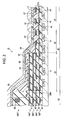
- Fig. 2 shows a schematic sectional configuration of the solid-state imaging device 10 according to the present embodiment.
- Fig. 2 is a sectional view of the section taken along a line II-II shown in Fig. 1 and is a sectional view in the periphery of the boundary between the sensor portion region 20 and the peripheral circuit regions 30.
- the solid-state imaging device 10 is provided with a semiconductor substrate 11, wiring layer portions 21a, 23a, and 30a, a passivation film 51, a layer of color filter 52, and a layer of on-chip lens 53.
- the wiring layer portions 21a, 23a, and 30a, the passivation film 51, the layer of color filter 52, and the layer of on-chip lens 53 are laminated on the semiconductor substrate 11 in that order.
- the semiconductor substrate 11 (substrate) is formed from, for example, a silicon substrate, and on the surface thereof, a plurality of pixels 40 including photodiodes 41 and pixel transistors (MOS transistors: not shown in the drawing) are arranged two-dimensionally.
- the passivation film 51 is formed from, for example, silicon nitride (SiN: refractive index 2.0), which is a material having a refractive index higher than that of silicon oxide (SiO 2 : refractive index 1.45) or the like serving as a material for forming an interlayer insulating layer 42, as described later.
- the color filter 52 is formed from, for example, a photoresist containing a colorant.
- the on-chip lens 53 is formed from, for example, silicon oxide (SiO 2 ).
- SiO 2 silicon oxide
- the on-chip lens 53 is disposed in the invalid pixel region 22.
- no on-chip lens 53 may be disposed in the invalid pixel region 22 if the color filter 52 has a light-condensing function.
- the film configurations of the wiring layer portions 21a, 23a, and 30a disposed on the semiconductor substrate 11 are different depending on the regions constituting the solid-state imaging device 10, as shown in Fig. 3 .
- the film configurations of wiring layer portions disposed in the individual regions will be described.
- five wiring layers 1MT to 5MT constitute a wiring layer portion, as described later.
- the present invention is not limited to this and the number of wiring layers may be changed appropriately in accordance with, for example, uses and specifications appropriately.
- the wiring layer portion 21a on the effective pixel region 21 and the invalid pixel region 22 in the sensor portion region 20 is formed from a wiring layer 1MT including metal films 44 and the wiring layer 2MT including metal films 45.
- the wiring layer 2MT is laminated on the wiring layer 1MT with a capping film 43 and an interlayer insulating layer 42 therebetween. Furthermore, the wiring layer 1MT is disposed on the semiconductor substrate 11 with the interlayer insulating layer 42, and a capping film 43 and the interlayer insulating layer 42 are disposed between the wiring layer 2MT and the passivation film 51 from the wiring layer 2MT side.
- the metal films 44 and 45 constituting the wiring layers 1MT and 2MT, respectively are disposed at locations, at which the light incident on the photodiodes 41 through the on-chip lens 53 is not blocked.
- the metal films 44 and 45 are disposed at locations other than the regions in which the on-chip lens 53 and the photodiodes 41 are opposed to each other.
- concave portions 57 are disposed on the surface of the wiring layer portion 21a in the effective pixel region 21 and the invalid pixel region 22.
- the concave portion 57 is disposed between adjacent metal films 45.
- the concave portion 57 is disposed in such a way that the depth of the concave portion 57 reaches the capping film 43 disposed on the wiring layer 1MT.
- the wiring layer portions 23a on the OPB region 23 in the sensor portion region 20 is formed from the wiring layer 1MT including the metal films 44, the wiring layer 2MT including the metal films 45, the wiring layer 3MT including a light-shielding layer 49, and the wiring layer 4MT including a light-shielding layer 50. Then, the wiring layers 1MT to 4MT are laminated on the semiconductor substrate 11 in that order.
- the capping film 43 and the interlayer insulating layer 42 are disposed from the lower wiring layer side between the individual wiring layers. Furthermore, the wiring layer 1MT is disposed on the semiconductor substrate 11 with the interlayer insulating layer 42 therebetween, and the capping film 43 and the interlayer insulating layer 42 are disposed from the wiring layer 4MT side between the wiring layer 4MT and the passivation film 51.
- the metal films 44 and 45 constituting the wiring layers 1MT and 2MT, respectively, are disposed at locations other than the regions above the photodiodes 41.
- the wiring layer portions 30a on the peripheral circuit region 30 is provided with the wiring layer 1MT including the metal films 44, the wiring layer 2MT including the metal films 45, the wiring layer 3MT including metal films 46, and the wiring layer 4MT including metal films 47. Furthermore, wiring layer portions 30a is provided with the wiring layer 5MT including metal films 48. Then, in the wiring layer portions 30a, the wiring layers 1MT to 5MT are laminated on the semiconductor substrate 11 in that order.
- the capping film 43 and the interlayer insulating layer 42 are disposed from the lower wiring layer side between the individual wiring layers. Furthermore, the wiring layer 1MT is disposed on the semiconductor substrate 11 with the interlayer insulating layer 42 therebetween, and the interlayer insulating layer 42 is disposed between the wiring layer 5MT and the passivation film 51.
- the metal films 44 to 48 and the light-shielding layers 49 and 50 may be formed from, for example, copper (Cu) or aluminum (Al).
- Cu copper
- Al aluminum
- diffusion-preventing films (not shown in the drawing), formed from, for example, titanium nitride (TiN) are disposed in the vicinity of the individual films. Diffusion of copper into the interlayer insulating layer 42 may be suppressed by disposing the diffusion-preventing films.
- the configurations (shape, dimension, film thickness, and the like) of the light-shielding layer 49 of the wiring layer 3MT and the light-shielding layer 50 of the wiring layer 4MT are specified to be the same.
- the light-shielding layers 49 and 50 may be formed from a metal film covering the entire surface of the OPB region 23 or by arranging linear metal films into the shape of a grid.
- a wiring, to which no signal pulse is applied, that is, a wiring not in use, may be used as the light-shielding layer.
- the interlayer insulating layer 42 is formed from, for example, silicon oxide (SiO 2 ).
- the capping film 43 is formed from, for example, silicon carbide (SiC).
- the capping films 43 are disposed on the individual wiring layers and are used as etching stopper layers. In the case where this capping film 43 is disposed, an etching step in formation of height difference portions and concave portions in the individual wiring layers may be controlled easily. In this regard, in the configuration example shown in the present embodiment, the capping films 43 are disposed on all wiring layers in the sensor portion region 20. However, the present invention is not limited to this.
- the capping films 43 may be disposed on predetermined wiring layers or the configuration may include no capping film 43.
- the film configurations of the wiring layer portions 30a, 23a, and 21a disposed on the peripheral circuit region 30, the OPB region 23, and the effective pixel region 21 and the invalid pixel region 22, respectively, are different from each other. Furthermore, the film thicknesses thereof are decreased in the order of the wiring layer portions 30a, 23a, and 21a.
- a first height difference portion 55 is disposed in the vicinity of the boundary between the peripheral circuit region 30 and the OPB region 23 because of a difference between thicknesses of the wiring layer portions of the two regions.
- a second height difference portion 56 is also disposed in the vicinity of the boundary between the OPB region 23 and the invalid pixel region 22 because of a difference between thicknesses of the wiring layer portions of the two regions.
- concave portions 57 are disposed on the surface of the wiring layer portions 21a in the effective pixel region 21 and the invalid pixel region 22.
- a plurality of height difference portions are disposed in such a way that the heights of surfaces of the wiring layer portions are reduced gradually from the peripheral circuit region 30 toward the effective pixel region 21 in the sensor portion region 20.
- concave portions 57 are disposed in the effective pixel region 21.
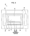
- Fig. 3 shows positional relationships among the individual constituent regions, the first and the second height difference portions 55 and 56, and the concave portions 57 in the solid-state imaging device 10 according to the present embodiment.
- Fig. 3 is a schematic upper surface configuration diagram of the solid-state imaging device 10, and the first and the second height difference portions 55 and 56 and the concave portions 57 are indicated by broken lines.
- the first height difference portion 55 is disposed along the vicinity of the peripheral portion of the sensor portion region 20.
- the second height difference portion 56 is disposed in such a way as to surround the effective pixel region 21.
- a plurality of concave portions 57 are disposed two-dimensionally at predetermined intervals in the effective pixel region 21 and the invalid pixel region 22 surrounded by the second height difference portion 56.
- the shape of opening of the concave portion 57 is square.
- the shape of opening of the concave portion 57 may be, for example, circular or polygonal, or the concave portion 57 may be formed into a groove.
- the height difference (distance, thickness) of the first height difference portion 55 is between 30nm and 5000nm
- the height difference (distance, thickness) of the second height difference portion 56 is between 100nm and 1000nm
- the depth of each concave portion is between 50nm and 500nm.
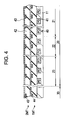
- Figs. 4 to 12 are diagrams showing film formation states after individual steps in the method for manufacturing the solid-state imaging device 10.
- Figs. 4 to 12 show schematic sectional views in the periphery of the boundary between the sensor portion region 20 and the peripheral circuit region 30.
- a plurality of pixels 40 including photodiodes 41 and pixel transistors are formed two-dimensionally in the sensor portion region 20 on the surface of the semiconductor substrate 11.
- the interlayer insulating layer 42, the metal films 44 (wiring layer 1MT having a film thickness between 100nm and 1000nm) and the capping film 43 are formed on the semiconductor substrate 11 in that order by a technique, e.g., sputtering.
- the interlayer insulating layer 42, the metal films 45 (wiring layer 2MT having a film thickness between 50nm and 500nm) and the capping film 43 are formed on the capping film 43 formed on the surface of the wiring layer 1MT in that order by a technique, e.g., sputtering.
- Fig. 4 shows the film formation state after the above-described step.
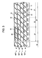
- the interlayer insulating layer 42, the wiring layer 3MT including the metal films 46 and the light-shielding layer 49, and the capping film 43 are formed on the capping film 43 formed on the surface of the wiring layer 2MT in that order by a technique, e.g., sputtering.
- the interlayer insulating layer 42, the wiring layer 4MT including the metal films 47 and the light-shielding layer 50, and the capping film 43 are formed on the capping film 43 formed on the surface of the wiring layer 3MT in that order by a technique, e.g., sputtering.
- Fig. 5 shows the film formation state after the above-described step.
- the film thickness of each wiring layer 3MT or 4MT is between 50nm and 500nm.
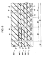
- the interlayer insulating layer 42 and the metal films 48 are formed on the capping film 43 formed on the surface of the wiring layer 4MT in that order by a technique, e.g., sputtering.
- the interlayer insulating layer 42 is formed on the metal films 48 (wiring layer 5MT) by a technique, e.g., sputtering.
- Fig. 6 shows the film formation state after the above-described step.
- the wiring layer portions are formed on the semiconductor substrate 11 by the above-described steps.
- the peripheral circuit region 30 is masked with a resist or the like, and the surface on the wiring layer portion side is etched through, for example, dry etching or wet etching.
- the wiring layer portion disposed on the sensor portion region 20 is etched from the interlayer insulating layer 42 located as the uppermost layer thereof.
- the etching is finished while the interlayer insulating layer 42 having some thickness is left on the capping film 43 disposed on the surface of the wiring layer 4MT.
- etching may be conducted until the capping film 43 is reached in such a way that the interlayer insulating layer 42 is not left.
- Fig. 7 shows the film formation state after the above-described etching step.
- the first height difference portion 55 having a height difference(distance, thickness) between 30nm and 5000nm is formed at the boundary between the sensor portion region 20 (OPB region 23) and the peripheral circuit region 30 by this step.
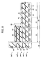
- the peripheral circuit region 30 and the OPB region 23 are masked with a resist or the like, and the surface on the wiring layer portion side is etched through, for example, dry etching or wet etching.
- the wiring layer portion disposed on the invalid pixel region 22 and the effective pixel region 21 are etched from the interlayer insulating layer 42 located as the uppermost layer thereof.
- the etching is finished while the interlayer insulating layer 42 having some thickness is left on the capping film 43 disposed on the surface of the wiring layer 2MT.
- etching may be conducted until the capping film 43 is reached in such a way that the interlayer insulating layer 42 is not left.
- the second height difference portion 56 having a height difference(distance, thickness) between 100nm and 1000nm is formed at the boundary between the OPB region 23 and the invalid pixel region 22 by this step.
- etching is finished when the etching reaches the capping film 43 disposed on the surface of the wiring layer 1MT.
- Fig. 9 shows the film formation state after the above-described etching step.
- the concave portions 57 having a depth between 50nm and 500m are formed in the regions above the photodiodes 41 in the effective pixel region 21 and the invalid pixel region 22 by this step.
- the etching may be finished while the interlayer insulating layer 42 having some thickness is left on the capping film 43 disposed on the surface of the wiring layer 1MT.
- the first height difference portion 55, the second height difference portion 56, and the concave portions 57 are formed at predetermined locations, as described above.
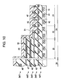
- the passivation film 51 is formed on the wiring layer portion provided with the first height difference portion 55, the second height difference portion 56, and the concave portions 57 by, for example, a chemical vapor deposition (CVD) method.
- the passivation film 51 is formed all over the surfaces of the sensor portion region 20 and the peripheral circuit region 30.
- the passivation film 51 is formed having such a thickness that the concave portions 57 are filled with the passivation film 51 and the surface of the passivation film 51 in the effective pixel region 21 becomes flat.
- Fig. 10 shows the film formation state after the above-described step.
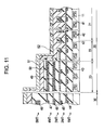
- a color filter material formed from, for example, a photoresist containing a colorant is applied to the passivation film 51, and exposure and development are conducted.
- the color filter 52 is formed at a predetermined location on the invalid pixel region 22 and the effective pixel region 21.
- Fig. 11 shows the film formation state after the above-described step.
- the two height difference portions are disposed in such a way that the heights of surfaces of the wiring layer portions are reduced gradually from the peripheral circuit region 30 toward the effective pixel region 21. Consequently, when the color filter material is applied to the passivation film 51 in the production step of the color filter 52, the amount of the color filter material built up in the vicinity of the individual height difference portions is reduced. As a result, the thickness of the color filter material applied to the effective pixel region 21 becomes uniform and the flatness of the color filter 52 is ensured.
- an on-chip lens material is applied to the layer of color filter 52.
- the amount of the on-chip lens material built up in the vicinity of the individual height difference portions is reduced, and the thickness of the on-chip lens material applied to the effective pixel region 21 becomes uniform.
- Fig. 12 shows the film formation state after the above-described step.
- the solid-state imaging device 10 is produced as described above.
- the thickness of the wiring layer portion 21a disposed in the effective pixel region 21 and the invalid pixel region 22 is specified to be smaller than that in the OPB region 23, as described above. Therefore, in the solid-state imaging device 10 according to the present embodiment, the distance between the on-chip lens 53 and the photodiode 41 in the effective pixel region 21 may be further reduced as compared with that in Fig. 28 . That is, in the present embodiment, the distance of optical path from the light incident side surface to the pixel 40 in the effective pixel region 21 may be further reduced and light scattering interface on the optical path may be reduced. As a result, in the present embodiment, pixel characteristics, e.g., sensitivity, may be further improved.
- the plurality of height difference portions (first and second height difference portions 55 and 56) are disposed on the surfaces of the wiring layer portions over from the peripheral circuit region 30 to the effective pixel region 21 in the sensor portion region 20.
- Such a configuration exerts the following effects.
- the solid-state imaging device 200 depicted in Fig. 28 it is also considered to increase the height difference at the boundary between the peripheral circuit region 230 and the sensor portion region 220 as a technique to reduce the distance between the on-chip lens 209 and the photodiode 202.
- problems e.g., brushing unevenness or frame unevenness, occur in the case where the layer of color filter 208 or the layer of on-chip lens 209 is formed by a coating method. In this case, problems occur in that the flatness of the coating material is reduced and the optical characteristics deteriorate.
- the solid-state imaging device 10 has the configuration, in which a plurality of height difference portions are disposed in such a way that the heights of surfaces of the wiring layer portions are reduced stepwise gradually from the peripheral circuit region 30 toward the effective pixel region 21 in the sensor portion region 20.
- the height differences of the individual height difference portions can be made smaller and, therefore, an occurrence of the above-described problems in the formation of the layer of color filter 52 or the layer of on-chip lens 53 through coating may be avoided. As a result, deterioration of the optical characteristics may be suppressed.
- the concave portions 57 are disposed on the surface of the wiring layer portion 21a in the effective pixel region 21 and the invalid pixel region 22, the capping film 43 on the wiring layer 2MT in the regions above the photodiodes 41 are removed, as in the present embodiment. Consequently, in the present embodiment, deterioration of the optical characteristics may be further suppressed.
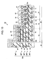
- Fig. 13 shows a schematic sectional configuration of a solid-state imaging device according to a second embodiment.
- the same configurations as those in the above-described first embodiment are indicated by the same reference numerals as those set forth above.
- a solid-state imaging device 60 is provided with a semiconductor substrate 11, wiring layer portions 21a, 23a, and 30a, a passivation film 61, a light waveguide layer 62, a layer of color filter 52, and a layer of on-chip lens 53.
- the wiring layer portions 21a, 23a, and 30a, the passivation film 61, the light waveguide layer 62, the layer of color filter 52, and the layer of on-chip lens 53 are laminated on the semiconductor substrate 11 in that order.
- individual regions constituting the solid-state imaging device 60 according to the present embodiment are the same as the configuration according to the above-described first embodiment ( Fig. 1 ).
- the configurations other than the configurations of the passivation film 61 and the light waveguide layer 62 are the same as the configurations ( Figs. 2 and 12 ) in the above-described first embodiment. Therefore, merely the passivation film 61 and the light waveguide layer 62 will be explained here.
- the passivation film 61 may be formed from the same material as the material for the passivation film 51 used in the above-described first embodiment. Specifically, the passivation film 61 is formed from, for example, silicon nitride (SiN: refractive index 2.0) or the like having a refractive index higher than that of silicon oxide (SiO 2 : 1.45) or the like, which is the material for forming the interlayer insulating layer 42.
- SiN silicon nitride
- SiO 2 silicon oxide
- the film thickness of the passivation film 51 is specified to be large and the concave portions 57 disposed on the surface of the wiring layer portion 21a in the effective pixel region 21 and the invalid pixel region 22 are filled with the passivation film 51.
- the film thickness of the passivation film 61 is specified to be small and the passivation film 61 is disposed in such a way as to cover the surfaces of the wiring layer portions 21a, 23a, and 30a. Consequently, in the present embodiment, concave portions are disposed on the surface of the passivation film 61 as well.
- the film thickness of the passivation film 61 may be, for example, about 0.5 ⁇ m.
- the light waveguide layer 62 is disposed on the passivation film 61 while having such a thickness that fills the concave portions disposed on the surface of the passivation film 61.
- the material for forming the light waveguide layer 62 for example, a material having a refractive index higher than that of silicon oxide (SiO 2 1.45) or the like, which is the material for forming the interlayer insulating layer 42, is used.
- siloxane resins, polyimide resins, and the like may be used as the material for forming the light waveguide layer 62.
- the above-described resin materials may contain, for example, metal oxide fine particles, e.g., titanium oxide, tantalum oxide, niobium oxide, tungsten oxide, zirconium oxide, zinc oxide, indium oxide, and hafnium oxide.
- metal oxide fine particles e.g., titanium oxide, tantalum oxide, niobium oxide, tungsten oxide, zirconium oxide, zinc oxide, indium oxide, and hafnium oxide.
- the refractive index of the light waveguide layer 62 is made higher.
- Figs. 14 and 15 show merely steps different from the above-described method for manufacturing the solid-state imaging device 10 according to the first embodiment ( figs. 4 to 12 ).
- the first height difference portion 55, the second height difference portion 56, and the concave portions 57 are formed at predetermined locations on the wiring layer portion (refer to Fig. 9 ) in a manner similar to the steps explained in the first embodiment with reference to Figs. 4 to 9 .
- the passivation film 61 is formed on the resulting wiring layer portion by, for example, the CVD method. At this time, the passivation film 61 is formed all over the surfaces of the sensor portion region 20 and the peripheral circuit region 30 while having such a thickness that covers the surfaces of the wiring layer portions.
- Fig. 14 shows the film formation state after the above-described step.
- a material for forming the light waveguide layer 62 is applied to the passivation film 61.
- the coating material is filled into the concave portions 57, and the light waveguide layer 62 having a flat surface is formed in the effective pixel region 21.
- Fig. 15 shows the film formation state after the above-described step.
- the layer of color filter 52 and the layer of on-chip lens 53 are formed on the light waveguide layer 62 in a manner similar to the steps explained in the first embodiment with reference to Figs. 11 and 12 .
- the solid-state imaging device 60 is formed as described above.
- the first height difference portion 55, the second height difference portion 56, and the concave portions 57 are formed on the surfaces of the wiring layer portions, and furthermore, the light waveguide layer 62 having a high refractive index is disposed in the region above the photodiodes 41. Consequently, in the present embodiment, the same effects as those of the first embodiment are obtained and, in addition, the solid-state imaging device 60 having further excellent optical characteristics may be provided.
- the concave portions 57 are formed on the surface of the wiring layer portion 21a in the invalid pixel region 22 as well.
- the following effects are also obtained by employing the above-described configuration.
- Fig. 16 shows the shape of a coating film in the case where the material for forming the light waveguide layer 62 is applied to the wiring layer portion 21a in the present embodiment.
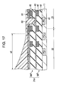
- Fig. 17 shows the shape of a coating film in the case where a concave portion 57 is not disposed on the surface of the wiring layer portion 21a in the invalid pixel region 22 and the material for forming the light waveguide layer 62 is applied.
- the invalid pixel region 22 does not include a portion to absorb the coating material built up in the vicinity of the second height difference portion 56. Consequently, as shown in Fig. 17 , the surface of the coating film does not become flat up to the vicinity of the boundary between the invalid pixel region 22 and the effective pixel region 21.
- the concave portions 57 may be formed from a groove.
- the concave portions 57 in the invalid pixel region 22 may be formed from a groove, or the concave portions 57 all over the surface of the invalid pixel region 22 and the effective pixel region 21 may be formed from grooves.
- the light-shielding layer 49 of the wiring layer 3MT and the light-shielding layer 50 of the wiring layer 4MT are specified to have the same configuration (shape, dimension, film thickness, and the like), although the present invention is not limited to this.
- a modified example 1 one configuration example in the case where the light-shielding layer of the wiring layer 3MT and the light-shielding layer of the wiring layer 4MT are specified to have different configurations will be explained.
- Fig. 18 shows a schematic film configuration of an OPB region 23 of a solid-state imaging device according to the present example.
- Fig. 18 shows the film configurations of merely the wiring layers 2MT to 4MT in order to simplify the explanation.
- the length of the light-shielding layer 65 of the wiring layer 3MT is specified to be larger than the length of the light-shielding layer 66 of the wiring layer 4MT. That is, in this example, the length of the light-shielding layer 65 located at the position farther from the light incident side is specified to be larger than the length of the light-shielding layer 66 located at the position nearer to the light incident side.
- the end portion, on the invalid pixel region 22 side, of the light-shielding layer 65 of the wiring layer 3MT is disposed on the side nearer to the invalid pixel region 22 than is the end portion, on the invalid pixel region 22 side, of the light-shielding layer 66 of the wiring layer 4MT.
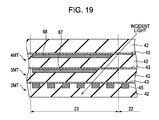
- Fig. 19 shows the film configuration of the OPB region 23 according to the comparative example.
- the case where the end portion, on the invalid pixel region 22 side, of the light-shielding layer 68 of the wiring layer 4MT is disposed on the side nearer to the invalid pixel region 22 than is the end portion, on the invalid pixel region 22 side, of the light-shielding layer 67 of the wiring layer 3MT will be considered.
- the incident light is not reflected by the light-shielding layers 67 and 68, but is incident on wiring layer 2MT in the OPB region 23 (refer to a solid line arrow shown in Fig. 19 ).
- the light-shielding property of the OPB region 23 in the vicinity of the boundary deteriorates.
- the configuration of the modified example 1 even if the light is incident from a slanting direction relative to the surface of the light-shielding layer 66, the light is reflected by the light-shielding layer 65 of the wiring layer 3MT (refer to a solid line arrow shown in Fig. 18 ), so that the incident light hardly reach the wiring layer 2MT in the OPB region 23. Therefore, the light-shielding property of the OPB region 23 in the vicinity of the boundary is improved by specifying the configuration of the light-shielding layer in the OPB region 23 to be the configuration according to the modified example 1.
- the configuration according to the modified example 1 the following advantages are also obtained.
- the length of the light-shielding layer 66 of the wiring layer 4MT is smaller than the length of the light-shielding layer 67 of the wiring layer 3MT. Therefore, in the OPB region 23, a region not provided with the light-shielding layer 66 of the wiring layer 4MT is present in the region of the interlayer insulating layer 42 on the light-shielding layer 65 of the wiring layer 3MT.
- Fig. 20 shows one configuration example thereof.
- Fig. 20 shows an example, in which in a region above the light-shielding layer 65 of the wiring layer 3MT, one height difference portion 70 is disposed in the region, which is not provided with the light-shielding layer 66 of the wiring layer 4MT, of the interlayer insulating layer 42.
- the present invention is not limited to this.
- a plurality of height difference portions may be disposed in a region not provided with the light-shielding layer 66 of the wiring layer 4MT.
- more height difference portions can be disposed on the surfaces of the wiring layer portions over from the peripheral circuit region 30 to the effective pixel region 21, so that the height difference of each height difference portion is made smaller. Therefore, in this case, the amount of coating material built up in the vicinity of the individual height difference portions may be further reduced. Consequently, the flatness of the coating film may be further improved in application of the layer of color filter 52 or the layer of on-chip lens 53.
- the angle between the height difference surface of the second height difference portion 56 disposed at the boundary between the invalid pixel region 22 and the OPB region 23 and the surface of the wiring layer portion 21a in the invalid pixel region 22 is specified to be about 90 degrees, although the present invention is not limited to this.
- the angle between the height difference surface of the second height difference portion and the surface of the wiring layer portion 21a in the invalid pixel region 22 may exceed 90 degrees. That is, the second height difference portion may be formed into a tapered shape.
- a modified example 2 one configuration example thereof will be described.
- Fig. 21 shows a schematic sectional configuration of the second height difference portion disposed at the boundary between the invalid pixel region 22 and the OPB region 23 in a solid-state imaging device according to the modified example 2.
- a coating film 76 e.g., the layer of color filter 52 or the layer of on-chip lens 53, is shown on the wiring layer portion.
- Such a taper-shaped second height difference portion 75 may be formed by, for example, inclining the end portion of a mask disposed on the wiring layer portion relative to a mask surface at a predetermined angle in the etching step.
- Fig. 22 shows a schematic sectional configuration of the second height difference portion 56 disposed at the boundary between the invalid pixel region 22 and the OPB region 23 in the above-described embodiment.
- the predetermined coating film 76 when the predetermined coating film 76 is applied to the wiring layer portion, some amount of coating material is built up in the vicinity of the second height difference portion 56. Consequently, it is necessary that the invalid pixel region 22 in the above-described embodiment has some area in order to flatten the coating film 76.
- the second height difference portion 75 is formed into a tapered shape. Therefore, in application of the coating material, flowing of the coating material in the vicinity of the second height difference portion 75 may become smoother. As a result, the amount of built-up of the coating material in the vicinity of the second height difference portion 75 may be reduced, as shown in Fig. 21 . Consequently, the area until the coating film 76 becomes flat may be reduced. That is, in the present example, the area of the invalid pixel region 22 may be further reduced.
- the taper-shaped height difference portion may be applied to the first height difference portion 55 disposed at the boundary between the peripheral circuit region 30 and the OPB region 23.
- the height difference portions are disposed at the boundary between the sensor portion region 20 (OPB region 23) and the peripheral circuit region 30 and at the boundary between the OPB region 23 and the invalid pixel region 22, although the present invention is not limited to this.
- a height difference portion may be disposed on the surface of the wiring layer portion 23a in the OPB region 23 in such a way that the surface height of the wiring layer portion 23a is reduced stepwise toward the invalid pixel region 22.
- a modified example 3 one configuration example thereof will be described.
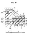
- Fig. 23 is a schematic sectional view in the vicinity of the boundary between the OPB region 23 and the peripheral circuit region 30 of the present example.
- Fig. 23 shows an example, in which besides a height difference portion 81 having a thickness between 15nm and 2500nm disposed at the boundary between the OPB region 23 and the peripheral circuit region 30, another height difference portion 82 having a thickness between 15nm and 2500nm is disposed on the surface of the wiring layer portion 23a in the OPB region 23.
- the present invention is not limited to this. At least two height difference portions may be disposed on the surface of the wiring layer portion 23a in the OPB region 23.
- the capping film 43 disposed on the wiring layer 1MT is left in the regions above the photodiodes 41, although the present invention is not limited to this.
- the capping film 43 disposed on the wiring layer 1MT may be removed through etching.
- Fig. 24 shows one configuration example (modified example 4) thereof.
- Fig. 24 shows a schematic sectional configuration of a film configuration disposed on one photodiode 41.
- Fig. 24 shows an example, in which the configuration of the modified example 4 is applied to the solid-state imaging device according to the above-described second embodiment.
- the configuration of the modified example 4 may be applied to the solid-state imaging device according to the first embodiment likewise.
- concave portion 85 in formation of concave portion 85 through, for example, etching in the effective pixel region 21, the etching is finished while an interlayer insulating layer 42 having some film thickness is left on the photodiode 41. Consequently, a capping film 43 disposed on the wiring layer 1MT in the region above the photodiode 41 may be removed. Thereafter, in a manner similar to that in the second embodiment, a passivation film 86, a light waveguide layer 87, a layer of color filter 52, and a layer of on-chip lens 53 are laminated on the concave portion 85 in that order.
- the capping film 43 is not present in the region above the photodiode 41. Therefore, the optical characteristics may be further improved.
- the solid-state imaging devices in which the OPB region 23 having the light-shielding layer is disposed in the sensor portion region 20, are described, although the present invention is not limited to them.
- the present invention can be applied to a solid-state imaging device, in which the OPB region 23 having the light-shielding layer is disposed in the peripheral circuit region 30, and the same effects are obtained.
- the solid-state imaging devices provided with the capping film 43 are described, although the present invention is not limited to them.
- the present invention can also be applied to a solid-state imaging device not provided with the capping film 43, and the same effects are obtained.
- the concave portions 57 are not necessarily disposed in the effective pixel region 21.
- the solid-state imaging device in which the concave portions 57 are disposed in the invalid pixel region 22, is described, although the present invention is not limited to this.
- the concave portions 57 are not necessarily disposed in the invalid pixel region 22.
- solid-state imaging devices may be applied to electronic apparatuses, e.g., cameras provided with solid-state imaging devices, portable apparatuses with cameras, and other electronic apparatuses provided with solid-state imaging devices.
- electronic apparatuses e.g., cameras provided with solid-state imaging devices, portable apparatuses with cameras, and other electronic apparatuses provided with solid-state imaging devices.
- an example, in which the solid-state imaging device according to an embodiment of the present invention is applied to a camera will be described as an example of such electronic apparatuses.
- FIG. 25 shows a schematic configuration of a camera according to the present embodiment.
- a camera 90 according to the present embodiment is provided with an optical system 91 (optical lens), a solid-state imaging device 92, and a signal processing circuit 93.
- optical system 91 optical lens
- solid-state imaging device 92 solid-state imaging device
- signal processing circuit 93 signal processing circuit
- the optical system 91 forms an image of image light (incident light) from a subject on an imaging surface of the solid-state imaging device 92. Consequently, a signal charge is accumulated for a predetermined period in a photodiode (photoelectric conversion element) of the solid-state imaging device 92.
- the solid-state imaging device according to any one of the above-described embodiments and the modified examples is applied to the solid-state imaging device 92. Then, the signal processing circuit 93 subjects output signals from the solid-state imaging device 92 to various signal processing treatments and outputs.
- the camera 90 according to the present embodiment may be not only used in the form of a camera alone, but also used in the form of a camera module, in which the optical system 91, the solid-state imaging device 92, and the signal processing circuit 93 are modularized.
- a modularized camera 90 according to the present embodiment may be applied to a portable apparatus with camera and the like typified by, for example, a cellular phone provided with the camera module.
- an electronic apparatus in which the pixel characteristics of the solid-state imaging device is excellent and sensitivity variation and color variation are reduced, may be provided.
Landscapes
- Solid State Image Pick-Up Elements (AREA)
- Transforming Light Signals Into Electric Signals (AREA)
Abstract
Description
- The present application claims priority to and contains subject matter related to that disclosed in Japanese Patent Application
JP 2009-115843 - The present invention relates to solid-state imaging devices, e.g., CMOS image sensors or CCD image sensors. The invention also relates to electronic apparatus including a solid-state imaging device, and a method for manufacturing a solid-state imaging device.
- Solid-state imaging devices, for example, complementary metal-oxide semiconductor (CMOS) image sensors and charge coupled device (CCD) image sensors, have been developed previously. A solid-state imaging device has a configuration, in which a photodiode (photoelectric conversion element) is disposed on the surface of a semiconductor substrate and when light is incident on the photodiode, an image signal is obtained on the basis of a signal charge generated in the photodiode. Furthermore, regarding a solid-state imaging device having the above-described configuration, in order to improve the optical characteristics, various configurations have been proposed previously (refer to Japanese Unexamined Patent Application Publication Nos.
2000-150846 2004-273791 -
Fig. 26 shows a schematic configuration sectional view of a solid-state imaging device proposed in Japanese Unexamined Patent Application Publication No.2000-150846 state imaging device 100 described in this document is composed of a light-receivingportion 101 includingphotoelectric conversion elements 104 arranged on the surface of asemiconductor substrate 103 one-dimensionally or two-dimensionally and aperipheral circuit portion 102 disposed in the periphery thereof. Furthermore, the solid-state imaging device 100 is provided withmicrolenses 108 and/or acolor filters 107 disposed on the light-receivingportion 101 with aninterlayer film 111 andwirings 105 therebetween. In this regard, theinterlayer film 111, anetching stopper layer 112, aprotective film 113, and a wiringlayer including wirings 106 are disposed on thesemiconductor substrate 103 of theperipheral circuit portion 102. - Moreover, regarding the solid-
state imaging device 100 described in Japanese Unexamined Patent Application Publication No.2000-150846 portion 101 is specified to be smaller than the thickness dc of the wiring layer of theperipheral circuit portion 102. Consequently, the light-condensing efficiency of themicrolens 108 is improved and a color-mixing problem of thecolor filter 107 is avoided. - In addition,
Fig. 27 shows a schematic sectional view in the vicinity of the boundary between a peripheral circuit portion and a sensor portion of a solid-state imaging device proposed in Japanese Unexamined Patent Application Publication No. 2004-273791. In the configuration of a solid-state imaging device 150 described in this document, a plurality ofwiring layers 161 to 163 are laminated on asubstrate 160 of aperipheral circuit portion 151 with flatteningfilm layers 165 therebetween, and the surface height of the laminated layer is reduced stepwise toward asensor portion 152. According to such a configuration, a sharp change in height at the boundary between theperipheral circuit portion 151 and thesensor portion 152 is reduced, and the film thickness of a predeterminedupper layer 164 disposed on thesensor portion 152 is made almost uniform all over the surface of thesensor portion 152, so as to facilitate an improvement of the optical characteristics. - As described above, Japanese Unexamined Patent Application Publication Nos.
2000-150846 2004-273791 Fig. 28 , while not prior art, is an illustrative example of the problem encountered by the inventors.Fig. 28 depicts a configuration sectional view of a solid-state imaging device in the case where the above-described technology is applied to the solid-state imaging device produced by the Cu wiring process. In this regard,Fig. 28 shows a configuration example in the case where a solid-state imaging device 200 is a CMOS image sensor. - The solid-
state imaging device 200 is provided with asemiconductor substrate 201 and a wiring layer portion includingmetal films 205 and light-shieldinglayers 206 deposited with interlayer insulatinglayers 203 and cappingfilms 204 therebetween. Furthermore, the solid-state imaging device 200 is provided with apassivation film 207, a layer ofcolor filter 208, and a layer of on-chip lens 209. Moreover, the wiring layer portion, thepassivation film 207, the layer ofcolor filter 208, and the layer of on-chip lens 209 are laminated on thesemiconductor substrate 201 in that order. In this regard,Fig. 28 shows an example in which the wiring layer portion is composed of five wiring layers 1MT to 5MT. - In addition, the solid-
state imaging device 200 is composed of asensor portion region 220 and aperipheral circuit region 230 including, for example, a vertical drive circuit and a horizontal drive circuit on asemiconductor substrate 201. A plurality ofpixels 240 includingphotodiodes 202 serving as photoelectric conversion elements and pixel transistors (MOS transistors: not shown in the drawing) are arranged two-dimensionally on the surface of thesemiconductor substrate 201 in thesensor portion region 220. - Furthermore, the
sensor portion region 220 includes aneffective pixel region 221, which outputs image signals actually, and aninvalid pixel region 222, which does not output an image signal actually. Moreover, thesensor portion region 220 includes an optical black region (hereafter referred to as OPB region) 223, which outputs a reference signal at a black level. In this regard, theinvalid pixel region 222 and theOPB region 223 are disposed at desired locations in the periphery of theeffective pixel region 221. - Then, in the solid-
state imaging device 200, the thickness of thewiring layer portion 220a in thesensor portion region 220 is specified to be smaller than the thickness of thewiring layer portion 230a in theperipheral circuit region 230. Consequently, aheight difference portion 210 is formed at the boundary between thesensor portion region 220 and theperipheral circuit region 230. - However, in the solid-
state imaging device 200 having the above-described configuration, the light-shieldinglayers 206 in theOPB region 223 are disposed as layers above the wiring layer 2MT and, thereby, it is difficult to reduce the distance between thephotodiode 202 and the on-chip lens 209 sufficiently. Consequently, regarding the solid-state imaging device 200 in the related art, a problem occurs in that the optical sensitivity of thephotodiode 202 is not improved sufficiently. - The present invention provides a solid state imaging device, and a method of producing the same, where the distance from the surface on the light incident side of the device to the pixel is reduced resulting in greater sensitivity.
- In accordance with systems consistent with the present disclosure, a solid state imaging device includes a semiconductor substrate having a plurality of photodiodes thereon and a first wiring portion, a second wiring portion and a third wiring portion, a first wiring layer over the semiconductor substrate and which includes a plurality of metal films and extends across all the wiring portions, and a second wiring layer over the first wiring layer and which extends across the first wiring portion and the second wiring portion.
- In accordance with systems consistent with the present disclosure, a method of creating a solid state imaging device includes the steps of forming a plurality of photodiodes in a third wiring portion of a semiconductor substrate which has a first wiring portion, a second wiring portion and the third wiring portion, forming over the semiconductor substrate a first wiring layer which includes a plurality of metal films and which extends across all the wiring portions, and forming over the first wiring layer a second wiring layer which extends over the first wiring portion and the second wiring portion.
- In accordance with systems consistent with the present disclosure, an electronic apparatus includes an optical system, a solid-state imaging device which receives light from the optical system, the solid-state imaging device including a semiconductor substrate having a plurality of photodiodes thereon and a first wiring portion, a second wiring portion and a third wiring portion, a first wiring layer over the semiconductor substrate and which includes a plurality of metal films and extends across all the wiring portions, and a second wiring layer over the first wiring layer and which extends across the first wiring portion and the second wiring portion.
- Other systems, methods, features, and advantages of the present application will be or will become apparent to one with skill in the art upon examination of the following figures and detailed description. It is intended that all such additional systems, methods, features, and advantages be included within this description, be within the scope of the disclosure, and be protected by the accompanying claims.
-
-
Fig. 1 is a schematic configuration diagram of a solid-state imaging device according to a first embodiment; -
Fig. 2 is a sectional view of the section taken along a line II-II shown inFig. 1 ; -
Fig. 3 is a diagram showing a positional relationship between individual regions constituting the solid-state imaging device according to the first embodiment and height difference portions and concave portions; -
Fig. 4 is a diagram for explaining a method for manufacturing the solid-state imaging device according to the first embodiment; -
Fig. 5 is a diagram for explaining the method for manufacturing the solid-state imaging device according to the first embodiment; -
Fig. 6 is a diagram for explaining the method for manufacturing the solid-state imaging device according to the first embodiment; -
Fig. 7 is a diagram for explaining the method for manufacturing the solid-state imaging device according to the first embodiment; -
Fig. 8 is a diagram for explaining the method for manufacturing the solid-state imaging device according to the first embodiment; -
Fig. 9 is a diagram for explaining the method for manufacturing the solid-state imaging device according to the first embodiment; -
Fig. 10 is a diagram for explaining the method for manufacturing the solid-state imaging device according to the first embodiment; -
Fig. 11 is a diagram for explaining the method for manufacturing the solid-state imaging device according to the first embodiment; -
Fig. 12 is a diagram for explaining the method for manufacturing the solid-state imaging device according to the first embodiment; -
Fig. 13 is a schematic configuration sectional view of a solid-state imaging device according to a second embodiment; -
Fig. 14 is a diagram for explaining a method for manufacturing the solid-state imaging device according to a second embodiment; -
Fig. 15 is a diagram for explaining the method for manufacturing the solid-state imaging device according to the second embodiment; -
Fig. 16 is a schematic sectional view showing the shape of a coating film in the vicinity of an invalid pixel region of the solid-state imaging device according to the second embodiment; -
Fig. 17 is a schematic sectional view showing the shape of a coating film in the vicinity of an invalid pixel region in the case where a concave portion is not disposed in the invalid pixel region; -
Fig. 18 is a schematic configuration diagram of an OPB region of a solid-state imaging device according to a modified example 1; -
Fig. 19 is a schematic configuration diagram of an OPB region of a solid-state imaging device according to a comparative example; -
Fig. 20 is a schematic configuration diagram in the case where a height difference portion is disposed in the OPB region of the solid-state imaging device according to the modified example 1; -
Fig. 21 is a configuration diagram of a height difference portion disposed at the boundary between an invalid pixel region and an OPB region of a solid-state imaging device according to a modified example 2; -
Fig. 22 is a configuration diagram of a height difference portion disposed at the boundary between an invalid pixel region and an OPB region of a solid-state imaging device according to the first embodiment; -
Fig. 23 is a configuration diagram of a height difference portion disposed at the boundary between a peripheral circuit region and an OPB region of a solid-state imaging device according to a modified example 3; -
Fig. 24 is a configuration diagram of a concave portion in an effective pixel region of a solid-state imaging device according to a modified example 4; -
Fig. 25 is a schematic configuration diagram of an electronic apparatus according to a third embodiment; -
Fig. 26 is a schematic configuration diagram of a solid-state imaging device in a related art; -
Fig. 27 is a schematic configuration diagram of a solid-state imaging device in a related art; and -
Fig. 28 is a schematic configuration diagram of a solid-state imaging device produced by Cu wiring process, having a height difference at the boundary between the sensor portion and the peripheral circuit portion. - The configuration examples of solid-state imaging devices according to embodiments of the present invention and an electronic apparatus including the same will be described below with reference to the drawings in the following order. In this regard, the present invention is not limited to the examples described below.
- 1. Basic configuration example of solid-state imaging device
- 2. Configuration example of solid-state imaging device including light waveguide layer
- 3. One configuration example of electronic apparatus including solid-state imaging device according to embodiment of present invention
-
Fig. 1 shows a schematic configuration of a solid-state imaging device according to a first embodiment. In the present embodiment, a solid-state imaging device 10 will be described with reference to a CMOS image sensor as an example. The solid-state imaging device 10 mainly includes a sensor portion region 20 (pixel array region) disposed on asemiconductor substrate 11 and aperipheral circuit region 30 disposed in the periphery thereof. - The
sensor portion region 20 is composed of aneffective pixel region 21, which outputs image signals , aninvalid pixel region 22, which does not output an image signal , and anOPB region 23, which outputs a reference signal at a black level. In this regard, theinvalid pixel region 22 and theOPB region 23 are disposed at desired locations in the periphery of theeffective pixel region 21. The disposition locations of theinvalid pixel region 22 and theOPB region 23 may be changed depending on the characteristics of the device. Furthermore, a plurality ofpixels 40, as described later, are arranged in a two-dimensional array on the surface of thesemiconductor substrate 11 in thesensor portion region 20. - Although not shown in the drawing, the
peripheral circuit region 30 includes, for example, a vertical drive circuit, a column signal processing circuit, a horizontal drive circuit, an output circuit, and a control circuit. - The vertical drive circuit includes, for example, a shift register, which selectively scans individual pixels of the
sensor portion region 20 sequentially on a line by line basis in the vertical direction (for example, the y direction shown inFig. 1 ) . Then, pixel signals on the basis of signal charges generated in accordance with the amount of received light in the photodiodes of the individual pixels are supplied to a column signal processing circuit. The column signal processing circuit is disposed, for example, on a pixel line basis, and conducts signal processing, e.g., noise removal and signal amplification, of signals output from one line of pixels based on the signals from each line of pixels in theOPB region 23. The horizontal drive circuit includes, for example, a shift register, and outputs horizontal scanning pulses sequentially, so as to select a predetermined column signal processing circuit among a plurality of column signal processing circuits in the predetermined order and to output a pixel signal. The output circuit sequentially outputs signals from the individual column signal processing circuits to predetermined signal processing circuits . Then, the control circuit controls the above-described individual circuits on the basis of vertical synchronized signals, horizontal synchronized signals, and a master clock. -
Fig. 2 shows a schematic sectional configuration of the solid-state imaging device 10 according to the present embodiment. In this regard,Fig. 2 is a sectional view of the section taken along a line II-II shown inFig. 1 and is a sectional view in the periphery of the boundary between thesensor portion region 20 and theperipheral circuit regions 30. - The solid-
state imaging device 10 is provided with asemiconductor substrate 11,wiring layer portions passivation film 51, a layer ofcolor filter 52, and a layer of on-chip lens 53. In this regard, thewiring layer portions passivation film 51, the layer ofcolor filter 52, and the layer of on-chip lens 53 are laminated on thesemiconductor substrate 11 in that order. - The semiconductor substrate 11 (substrate) is formed from, for example, a silicon substrate, and on the surface thereof, a plurality of
pixels 40 includingphotodiodes 41 and pixel transistors (MOS transistors: not shown in the drawing) are arranged two-dimensionally. - The
passivation film 51 is formed from, for example, silicon nitride (SiN: refractive index 2.0), which is a material having a refractive index higher than that of silicon oxide (SiO2: refractive index 1.45) or the like serving as a material for forming an interlayer insulatinglayer 42, as described later. - The
color filter 52 is formed from, for example, a photoresist containing a colorant. Furthermore, the on-chip lens 53 is formed from, for example, silicon oxide (SiO2). In the example shown in the present embodiment, the on-chip lens 53 is disposed in theinvalid pixel region 22. However, no on-chip lens 53 may be disposed in theinvalid pixel region 22 if thecolor filter 52 has a light-condensing function. - Moreover, in the present embodiment, the film configurations of the
wiring layer portions semiconductor substrate 11 are different depending on the regions constituting the solid-state imaging device 10, as shown inFig. 3 . Here, the film configurations of wiring layer portions disposed in the individual regions will be described. Regarding an example explained in the present embodiment, five wiring layers 1MT to 5MT constitute a wiring layer portion, as described later. However, the present invention is not limited to this and the number of wiring layers may be changed appropriately in accordance with, for example, uses and specifications appropriately. - The
wiring layer portion 21a on theeffective pixel region 21 and theinvalid pixel region 22 in thesensor portion region 20 is formed from a wiring layer 1MT includingmetal films 44 and the wiring layer 2MT includingmetal films 45. The wiring layer 2MT is laminated on the wiring layer 1MT with acapping film 43 and an interlayer insulatinglayer 42 therebetween. Furthermore, the wiring layer 1MT is disposed on thesemiconductor substrate 11 with the interlayer insulatinglayer 42, and acapping film 43 and the interlayer insulatinglayer 42 are disposed between the wiring layer 2MT and thepassivation film 51 from the wiring layer 2MT side. - In this regard, in the
wiring layer portion 21a, themetal films photodiodes 41 through the on-chip lens 53 is not blocked. Specifically, themetal films chip lens 53 and thephotodiodes 41 are opposed to each other. - Moreover, in the present embodiment,
concave portions 57 are disposed on the surface of thewiring layer portion 21a in theeffective pixel region 21 and theinvalid pixel region 22. Theconcave portion 57 is disposed betweenadjacent metal films 45. In this regard, theconcave portion 57 is disposed in such a way that the depth of theconcave portion 57 reaches thecapping film 43 disposed on the wiring layer 1MT. - The
wiring layer portions 23a on theOPB region 23 in thesensor portion region 20 is formed from the wiring layer 1MT including themetal films 44, the wiring layer 2MT including themetal films 45, the wiring layer 3MT including a light-shielding layer 49, and the wiring layer 4MT including a light-shielding layer 50. Then, the wiring layers 1MT to 4MT are laminated on thesemiconductor substrate 11 in that order. - In this regard, in the
wiring layer portions 23a, the cappingfilm 43 and the interlayer insulatinglayer 42 are disposed from the lower wiring layer side between the individual wiring layers. Furthermore, the wiring layer 1MT is disposed on thesemiconductor substrate 11 with the interlayer insulatinglayer 42 therebetween, and thecapping film 43 and the interlayer insulatinglayer 42 are disposed from the wiring layer 4MT side between the wiring layer 4MT and thepassivation film 51. In this regard, in thewiring layer portion 23a, themetal films photodiodes 41. - The
wiring layer portions 30a on theperipheral circuit region 30 is provided with the wiring layer 1MT including themetal films 44, the wiring layer 2MT including themetal films 45, the wiring layer 3MT includingmetal films 46, and the wiring layer 4MT includingmetal films 47. Furthermore,wiring layer portions 30a is provided with the wiring layer 5MT includingmetal films 48. Then, in thewiring layer portions 30a, the wiring layers 1MT to 5MT are laminated on thesemiconductor substrate 11 in that order. - In this regard, in the
wiring layer portions 30a, the cappingfilm 43 and the interlayer insulatinglayer 42 are disposed from the lower wiring layer side between the individual wiring layers. Furthermore, the wiring layer 1MT is disposed on thesemiconductor substrate 11 with the interlayer insulatinglayer 42 therebetween, and the interlayer insulatinglayer 42 is disposed between the wiring layer 5MT and thepassivation film 51. - In the above-described wiring layer portions in the individual regions, the
metal films 44 to 48 and the light-shieldinglayers metal films 44 to 48 and the light-shieldinglayers interlayer insulating layer 42 may be suppressed by disposing the diffusion-preventing films. - In the present embodiment, the configurations (shape, dimension, film thickness, and the like) of the light-
shielding layer 49 of the wiring layer 3MT and the light-shielding layer 50 of the wiring layer 4MT are specified to be the same. The light-shieldinglayers OPB region 23 or by arranging linear metal films into the shape of a grid. Alternatively, a wiring, to which no signal pulse is applied, that is, a wiring not in use, may be used as the light-shielding layer. - The interlayer insulating
layer 42 is formed from, for example, silicon oxide (SiO2). The cappingfilm 43 is formed from, for example, silicon carbide (SiC). The cappingfilms 43 are disposed on the individual wiring layers and are used as etching stopper layers. In the case where thiscapping film 43 is disposed, an etching step in formation of height difference portions and concave portions in the individual wiring layers may be controlled easily. In this regard, in the configuration example shown in the present embodiment, the cappingfilms 43 are disposed on all wiring layers in thesensor portion region 20. However, the present invention is not limited to this. The cappingfilms 43 may be disposed on predetermined wiring layers or the configuration may include no cappingfilm 43. - As described above, in the solid-
state imaging device 10 according to the present embodiment, the film configurations of thewiring layer portions peripheral circuit region 30, theOPB region 23, and theeffective pixel region 21 and theinvalid pixel region 22, respectively, are different from each other. Furthermore, the film thicknesses thereof are decreased in the order of thewiring layer portions - As a result, a first
height difference portion 55 is disposed in the vicinity of the boundary between theperipheral circuit region 30 and theOPB region 23 because of a difference between thicknesses of the wiring layer portions of the two regions. Furthermore, a secondheight difference portion 56 is also disposed in the vicinity of the boundary between theOPB region 23 and theinvalid pixel region 22 because of a difference between thicknesses of the wiring layer portions of the two regions. Moreover, in the present embodiment,concave portions 57 are disposed on the surface of thewiring layer portions 21a in theeffective pixel region 21 and theinvalid pixel region 22. - That is, in the solid-
state imaging device 10, a plurality of height difference portions are disposed in such a way that the heights of surfaces of the wiring layer portions are reduced gradually from theperipheral circuit region 30 toward theeffective pixel region 21 in thesensor portion region 20. In addition,concave portions 57 are disposed in theeffective pixel region 21. - Here,
Fig. 3 shows positional relationships among the individual constituent regions, the first and the secondheight difference portions concave portions 57 in the solid-state imaging device 10 according to the present embodiment.Fig. 3 is a schematic upper surface configuration diagram of the solid-state imaging device 10, and the first and the secondheight difference portions concave portions 57 are indicated by broken lines. - In the present embodiment, as shown in
Fig. 3 , the firstheight difference portion 55 is disposed along the vicinity of the peripheral portion of thesensor portion region 20. The secondheight difference portion 56 is disposed in such a way as to surround theeffective pixel region 21. Furthermore, a plurality ofconcave portions 57 are disposed two-dimensionally at predetermined intervals in theeffective pixel region 21 and theinvalid pixel region 22 surrounded by the secondheight difference portion 56. In this regard, in the example shown inFig. 3 , the shape of opening of theconcave portion 57 is square. However, the present invention is not limited to this. The shape of opening of theconcave portion 57 may be, for example, circular or polygonal, or theconcave portion 57 may be formed into a groove.
Further, in the present embodiment, the height difference (distance, thickness) of the firstheight difference portion 55 is between 30nm and 5000nm, the height difference (distance, thickness) of the secondheight difference portion 56 is between 100nm and 1000nm, and the depth of each concave portion is between 50nm and 500nm. - Next, a method for manufacturing the solid-
state imaging device 10 according to the present embodiment will be described with reference toFigs. 4 to 12. Figs. 4 to 12 are diagrams showing film formation states after individual steps in the method for manufacturing the solid-state imaging device 10. In this regard,Figs. 4 to 12 show schematic sectional views in the periphery of the boundary between thesensor portion region 20 and theperipheral circuit region 30. - Initially, a plurality of
pixels 40 includingphotodiodes 41 and pixel transistors (not shown in the drawing) are formed two-dimensionally in thesensor portion region 20 on the surface of thesemiconductor substrate 11. Thereafter, theinterlayer insulating layer 42, the metal films 44 (wiring layer 1MT having a film thickness between 100nm and 1000nm) and thecapping film 43 are formed on thesemiconductor substrate 11 in that order by a technique, e.g., sputtering. Furthermore, theinterlayer insulating layer 42, the metal films 45 (wiring layer 2MT having a film thickness between 50nm and 500nm) and thecapping film 43 are formed on thecapping film 43 formed on the surface of the wiring layer 1MT in that order by a technique, e.g., sputtering.Fig. 4 shows the film formation state after the above-described step. - Subsequently, the
interlayer insulating layer 42, the wiring layer 3MT including themetal films 46 and the light-shielding layer 49, and thecapping film 43 are formed on thecapping film 43 formed on the surface of the wiring layer 2MT in that order by a technique, e.g., sputtering. Moreover, theinterlayer insulating layer 42, the wiring layer 4MT including themetal films 47 and the light-shielding layer 50, and thecapping film 43 are formed on thecapping film 43 formed on the surface of the wiring layer 3MT in that order by a technique, e.g., sputtering.Fig. 5 shows the film formation state after the above-described step. The film thickness of each wiring layer 3MT or 4MT is between 50nm and 500nm. - Then, the
interlayer insulating layer 42 and the metal films 48 (wiring layer 5MT having a film thickness between 50nm and 6000nm) are formed on thecapping film 43 formed on the surface of the wiring layer 4MT in that order by a technique, e.g., sputtering. In addition, in the present embodiment, theinterlayer insulating layer 42 is formed on the metal films 48 (wiring layer 5MT) by a technique, e.g., sputtering.Fig. 6 shows the film formation state after the above-described step. In the present embodiment, the wiring layer portions are formed on thesemiconductor substrate 11 by the above-described steps. - Next, the
peripheral circuit region 30 is masked with a resist or the like, and the surface on the wiring layer portion side is etched through, for example, dry etching or wet etching. In this manner, the wiring layer portion disposed on thesensor portion region 20 is etched from the interlayer insulatinglayer 42 located as the uppermost layer thereof. Then, the etching is finished while theinterlayer insulating layer 42 having some thickness is left on thecapping film 43 disposed on the surface of the wiring layer 4MT. In this regard, etching may be conducted until thecapping film 43 is reached in such a way that the interlayer insulatinglayer 42 is not left.Fig. 7 shows the film formation state after the above-described etching step. The firstheight difference portion 55 having a height difference(distance, thickness) between 30nm and 5000nm is formed at the boundary between the sensor portion region 20 (OPB region 23) and theperipheral circuit region 30 by this step. - Subsequently, the
peripheral circuit region 30 and theOPB region 23 are masked with a resist or the like, and the surface on the wiring layer portion side is etched through, for example, dry etching or wet etching. In this manner, the wiring layer portion disposed on theinvalid pixel region 22 and theeffective pixel region 21 are etched from the interlayer insulatinglayer 42 located as the uppermost layer thereof. Then, the etching is finished while theinterlayer insulating layer 42 having some thickness is left on thecapping film 43 disposed on the surface of the wiring layer 2MT. In this regard, etching may be conducted until thecapping film 43 is reached in such a way that the interlayer insulatinglayer 42 is not left.Fig. 8 shows the film formation state after the above-described etching step. The secondheight difference portion 56 having a height difference(distance, thickness) between 100nm and 1000nm is formed at the boundary between theOPB region 23 and theinvalid pixel region 22 by this step. - Thereafter, the region other than the regions above the
photodiodes 41 in theeffective pixel region 21 and theinvalid pixel region 22 are masked with a resist or the like, and the surface of the wiring layer portion side is etched through, for example, dry etching or wet etching. Consequently, the regions of mask opening portions (regions above the photodiodes 41) are etched. Then, etching is finished when the etching reaches thecapping film 43 disposed on the surface of the wiring layer 1MT.Fig. 9 shows the film formation state after the above-described etching step. Theconcave portions 57 having a depth between 50nm and 500m are formed in the regions above thephotodiodes 41 in theeffective pixel region 21 and theinvalid pixel region 22 by this step. In this regard, in the formation of theconcave portions 57, the etching may be finished while theinterlayer insulating layer 42 having some thickness is left on thecapping film 43 disposed on the surface of the wiring layer 1MT. In the present embodiment, the firstheight difference portion 55, the secondheight difference portion 56, and theconcave portions 57 are formed at predetermined locations, as described above. - Next, the
passivation film 51 is formed on the wiring layer portion provided with the firstheight difference portion 55, the secondheight difference portion 56, and theconcave portions 57 by, for example, a chemical vapor deposition (CVD) method. At this time, thepassivation film 51 is formed all over the surfaces of thesensor portion region 20 and theperipheral circuit region 30. Furthermore, at this time, thepassivation film 51 is formed having such a thickness that theconcave portions 57 are filled with thepassivation film 51 and the surface of thepassivation film 51 in theeffective pixel region 21 becomes flat.Fig. 10 shows the film formation state after the above-described step. - Subsequently, a color filter material formed from, for example, a photoresist containing a colorant is applied to the
passivation film 51, and exposure and development are conducted. In this manner, thecolor filter 52 is formed at a predetermined location on theinvalid pixel region 22 and theeffective pixel region 21.Fig. 11 shows the film formation state after the above-described step. - In this regard, as described above, in the configuration of the present embodiment, the two height difference portions are disposed in such a way that the heights of surfaces of the wiring layer portions are reduced gradually from the
peripheral circuit region 30 toward theeffective pixel region 21. Consequently, when the color filter material is applied to thepassivation film 51 in the production step of thecolor filter 52, the amount of the color filter material built up in the vicinity of the individual height difference portions is reduced. As a result, the thickness of the color filter material applied to theeffective pixel region 21 becomes uniform and the flatness of thecolor filter 52 is ensured. - Then, an on-chip lens material is applied to the layer of
color filter 52. In this step as well, the amount of the on-chip lens material built up in the vicinity of the individual height difference portions is reduced, and the thickness of the on-chip lens material applied to theeffective pixel region 21 becomes uniform. - Thereafter, the film surface of the on-chip lens material is patterned, so as to form the on-
chip lens 53 having a predetermined shape above thephotodiodes 41 in theeffective pixel region 21 and theinvalid pixel region 22.Fig. 12 shows the film formation state after the above-described step. In the present embodiment, the solid-state imaging device 10 is produced as described above. - In the solid-
state imaging device 10 according to the present embodiment, the thickness of thewiring layer portion 21a disposed in theeffective pixel region 21 and theinvalid pixel region 22 is specified to be smaller than that in theOPB region 23, as described above. Therefore, in the solid-state imaging device 10 according to the present embodiment, the distance between the on-chip lens 53 and thephotodiode 41 in theeffective pixel region 21 may be further reduced as compared with that inFig. 28 . That is, in the present embodiment, the distance of optical path from the light incident side surface to thepixel 40 in theeffective pixel region 21 may be further reduced and light scattering interface on the optical path may be reduced. As a result, in the present embodiment, pixel characteristics, e.g., sensitivity, may be further improved. - Furthermore, in the solid-
state imaging device 10 according to the present embodiment, the plurality of height difference portions (first and secondheight difference portions 55 and 56) are disposed on the surfaces of the wiring layer portions over from theperipheral circuit region 30 to theeffective pixel region 21 in thesensor portion region 20. Such a configuration exerts the following effects. - Regarding the solid-
state imaging device 200 depicted inFig. 28 , it is also considered to increase the height difference at the boundary between theperipheral circuit region 230 and thesensor portion region 220 as a technique to reduce the distance between the on-chip lens 209 and thephotodiode 202. However, if the height difference between the two regions increases, problems, e.g., brushing unevenness or frame unevenness, occur in the case where the layer ofcolor filter 208 or the layer of on-chip lens 209 is formed by a coating method. In this case, problems occur in that the flatness of the coating material is reduced and the optical characteristics deteriorate. - On the other hand, as described above, the solid-
state imaging device 10 according to the present invention has the configuration, in which a plurality of height difference portions are disposed in such a way that the heights of surfaces of the wiring layer portions are reduced stepwise gradually from theperipheral circuit region 30 toward theeffective pixel region 21 in thesensor portion region 20. In this case, the height differences of the individual height difference portions can be made smaller and, therefore, an occurrence of the above-described problems in the formation of the layer ofcolor filter 52 or the layer of on-chip lens 53 through coating may be avoided. As a result, deterioration of the optical characteristics may be suppressed. - Furthermore, in the case where the
concave portions 57 are disposed on the surface of thewiring layer portion 21a in theeffective pixel region 21 and theinvalid pixel region 22, the cappingfilm 43 on the wiring layer 2MT in the regions above thephotodiodes 41 are removed, as in the present embodiment. Consequently, in the present embodiment, deterioration of the optical characteristics may be further suppressed. -
Fig. 13 shows a schematic sectional configuration of a solid-state imaging device according to a second embodiment. In this regard, inFig. 13 , the same configurations as those in the above-described first embodiment (Figs. 2 and12 ) are indicated by the same reference numerals as those set forth above. - A solid-
state imaging device 60 is provided with asemiconductor substrate 11,wiring layer portions passivation film 61, alight waveguide layer 62, a layer ofcolor filter 52, and a layer of on-chip lens 53. Thewiring layer portions passivation film 61, thelight waveguide layer 62, the layer ofcolor filter 52, and the layer of on-chip lens 53 are laminated on thesemiconductor substrate 11 in that order. In this regard, individual regions constituting the solid-state imaging device 60 according to the present embodiment are the same as the configuration according to the above-described first embodiment (Fig. 1 ). - In the present embodiment, the configurations other than the configurations of the
passivation film 61 and thelight waveguide layer 62 are the same as the configurations (Figs. 2 and12 ) in the above-described first embodiment. Therefore, merely thepassivation film 61 and thelight waveguide layer 62 will be explained here. - The
passivation film 61 may be formed from the same material as the material for thepassivation film 51 used in the above-described first embodiment. Specifically, thepassivation film 61 is formed from, for example, silicon nitride (SiN: refractive index 2.0) or the like having a refractive index higher than that of silicon oxide (SiO2: 1.45) or the like, which is the material for forming the interlayer insulatinglayer 42. - In this regard, in the configuration of the above-described first embodiment, the film thickness of the
passivation film 51 is specified to be large and theconcave portions 57 disposed on the surface of thewiring layer portion 21a in theeffective pixel region 21 and theinvalid pixel region 22 are filled with thepassivation film 51. On the other hand, in the present embodiment, as shown inFig. 13 , the film thickness of thepassivation film 61 is specified to be small and thepassivation film 61 is disposed in such a way as to cover the surfaces of thewiring layer portions passivation film 61 as well. In this regard, the film thickness of thepassivation film 61 may be, for example, about 0.5 µm. - The
light waveguide layer 62 is disposed on thepassivation film 61 while having such a thickness that fills the concave portions disposed on the surface of thepassivation film 61. As for the material for forming thelight waveguide layer 62, for example, a material having a refractive index higher than that of silicon oxide (SiO2 1.45) or the like, which is the material for forming the interlayer insulatinglayer 42, is used. For example, siloxane resins, polyimide resins, and the like may be used as the material for forming thelight waveguide layer 62. Furthermore, as for the material for forming thelight waveguide layer 62, the above-described resin materials may contain, for example, metal oxide fine particles, e.g., titanium oxide, tantalum oxide, niobium oxide, tungsten oxide, zirconium oxide, zinc oxide, indium oxide, and hafnium oxide. In this case, the refractive index of thelight waveguide layer 62 is made higher. - Next, a method for manufacturing the solid-
state imaging device 60 according to the present embodiment will be described simply with reference toFigs. 14 and15 . In this regard,Figs. 14 and15 show merely steps different from the above-described method for manufacturing the solid-state imaging device 10 according to the first embodiment (figs. 4 to 12 ). - Initially, the first
height difference portion 55, the secondheight difference portion 56, and theconcave portions 57 are formed at predetermined locations on the wiring layer portion (refer toFig. 9 ) in a manner similar to the steps explained in the first embodiment with reference toFigs. 4 to 9 . Subsequently, thepassivation film 61 is formed on the resulting wiring layer portion by, for example, the CVD method. At this time, thepassivation film 61 is formed all over the surfaces of thesensor portion region 20 and theperipheral circuit region 30 while having such a thickness that covers the surfaces of the wiring layer portions.Fig. 14 shows the film formation state after the above-described step. - Then, a material for forming the
light waveguide layer 62 is applied to thepassivation film 61. In this manner, the coating material is filled into theconcave portions 57, and thelight waveguide layer 62 having a flat surface is formed in theeffective pixel region 21.Fig. 15 shows the film formation state after the above-described step. - Thereafter, the layer of
color filter 52 and the layer of on-chip lens 53 are formed on thelight waveguide layer 62 in a manner similar to the steps explained in the first embodiment with reference toFigs. 11 and12 . In the present embodiment, the solid-state imaging device 60 is formed as described above. - In the present embodiment, as described above, the first
height difference portion 55, the secondheight difference portion 56, and theconcave portions 57 are formed on the surfaces of the wiring layer portions, and furthermore, thelight waveguide layer 62 having a high refractive index is disposed in the region above thephotodiodes 41. Consequently, in the present embodiment, the same effects as those of the first embodiment are obtained and, in addition, the solid-state imaging device 60 having further excellent optical characteristics may be provided. - Moreover, in the present embodiment, as in the first embodiment, the
concave portions 57 are formed on the surface of thewiring layer portion 21a in theinvalid pixel region 22 as well. In the present embodiment, for example, the following effects are also obtained by employing the above-described configuration. -
Fig. 16 shows the shape of a coating film in the case where the material for forming thelight waveguide layer 62 is applied to thewiring layer portion 21a in the present embodiment. Furthermore,Fig. 17 shows the shape of a coating film in the case where aconcave portion 57 is not disposed on the surface of thewiring layer portion 21a in theinvalid pixel region 22 and the material for forming thelight waveguide layer 62 is applied. Regarding the configuration shown inFig. 17 , theinvalid pixel region 22 does not include a portion to absorb the coating material built up in the vicinity of the secondheight difference portion 56. Consequently, as shown inFig. 17 , the surface of the coating film does not become flat up to the vicinity of the boundary between theinvalid pixel region 22 and theeffective pixel region 21. - On the other hand, in the case where the
concave portions 57 are disposed on the surface of thewiring layer portion 21a in theinvalid pixel region 22, as in the present embodiment, a part of the coating material built up on the secondheight difference portion 56 is absorbed by (filled into) theconcave portions 57. As a result, regarding the configuration of the present embodiment, as shown inFig. 16 , an area from al to the area where the surface of the coating film becomes flat is smaller than an area a2 in the case shown inFig. 17 . Therefore, in the present embodiment, theinvalid pixel region 22 may be made small. - In this regard, in order to further improve the above-described effects, the
concave portions 57 may be formed from a groove. In this case, since the amount of absorption of the coating material by theconcave portion 57 increases, the area up to the are where the surface of the coating film becomes flat may be further reduced. In this case, merely theconcave portions 57 in theinvalid pixel region 22 may be formed from a groove, or theconcave portions 57 all over the surface of theinvalid pixel region 22 and theeffective pixel region 21 may be formed from grooves. - In examples explained in the above-described first and second embodiments, the light-
shielding layer 49 of the wiring layer 3MT and the light-shielding layer 50 of the wiring layer 4MT are specified to have the same configuration (shape, dimension, film thickness, and the like), although the present invention is not limited to this. In a modified example 1, one configuration example in the case where the light-shielding layer of the wiring layer 3MT and the light-shielding layer of the wiring layer 4MT are specified to have different configurations will be explained. -
Fig. 18 shows a schematic film configuration of anOPB region 23 of a solid-state imaging device according to the present example. In this regard,Fig. 18 shows the film configurations of merely the wiring layers 2MT to 4MT in order to simplify the explanation. - In this example, in the direction from the
OPB region 23 toward theinvalid pixel region 22, the length of the light-shielding layer 65 of the wiring layer 3MT is specified to be larger than the length of the light-shielding layer 66 of the wiring layer 4MT. That is, in this example, the length of the light-shielding layer 65 located at the position farther from the light incident side is specified to be larger than the length of the light-shielding layer 66 located at the position nearer to the light incident side. Then, the end portion, on theinvalid pixel region 22 side, of the light-shielding layer 65 of the wiring layer 3MT is disposed on the side nearer to theinvalid pixel region 22 than is the end portion, on theinvalid pixel region 22 side, of the light-shielding layer 66 of the wiring layer 4MT. - The following effects are obtained by employing the above-described configuration. Here, for purposes of comparison, the case where in a direction from the
OPB region 23 toward theinvalid pixel region 22, the light-shielding layer of the wiring layer 3MT is longer than the light-shielding layer of the wiring layer 4MT (comparative example) will be considered.Fig. 19 shows the film configuration of theOPB region 23 according to the comparative example. Furthermore, in the comparative example, the case where the end portion, on theinvalid pixel region 22 side, of the light-shielding layer 68 of the wiring layer 4MT is disposed on the side nearer to theinvalid pixel region 22 than is the end portion, on theinvalid pixel region 22 side, of the light-shielding layer 67 of the wiring layer 3MT will be considered. - Regarding the configuration of the comparative example, in the case where light is incident from a slanting direction relative to the surface of the light-
shielding layer 68 in the vicinity of the boundary between theOPB region 23 and theinvalid pixel region 22, the incident light is not reflected by the light-shieldinglayers Fig. 19 ). In this case, the light-shielding property of theOPB region 23 in the vicinity of the boundary deteriorates. - On the other hand, regarding the configuration of the modified example 1, even if the light is incident from a slanting direction relative to the surface of the light-
shielding layer 66, the light is reflected by the light-shielding layer 65 of the wiring layer 3MT (refer to a solid line arrow shown inFig. 18 ), so that the incident light hardly reach the wiring layer 2MT in theOPB region 23. Therefore, the light-shielding property of theOPB region 23 in the vicinity of the boundary is improved by specifying the configuration of the light-shielding layer in theOPB region 23 to be the configuration according to the modified example 1. - Moreover, regarding the configuration according to the modified example 1, the following advantages are also obtained. Regarding the
OPB region 23 in the modified example 1, in a direction from theOPB region 23 toward theinvalid pixel region 22, the length of the light-shielding layer 66 of the wiring layer 4MT is smaller than the length of the light-shielding layer 67 of the wiring layer 3MT. Therefore, in theOPB region 23, a region not provided with the light-shielding layer 66 of the wiring layer 4MT is present in the region of the interlayer insulatinglayer 42 on the light-shielding layer 65 of the wiring layer 3MT. Consequently, regarding the configuration according to the modified example 1, another height difference portion can be formed in the region, which is not provided with the light-shielding layer 66 of the wiring layer 4MT, of the interlayer insulatinglayer 42.Fig. 20 shows one configuration example thereof. -
Fig. 20 shows an example, in which in a region above the light-shielding layer 65 of the wiring layer 3MT, oneheight difference portion 70 is disposed in the region, which is not provided with the light-shielding layer 66 of the wiring layer 4MT, of the interlayer insulatinglayer 42. However, the present invention is not limited to this. A plurality of height difference portions may be disposed in a region not provided with the light-shielding layer 66 of the wiring layer 4MT. In the case where the above-described configuration is employed, more height difference portions can be disposed on the surfaces of the wiring layer portions over from theperipheral circuit region 30 to theeffective pixel region 21, so that the height difference of each height difference portion is made smaller. Therefore, in this case, the amount of coating material built up in the vicinity of the individual height difference portions may be further reduced. Consequently, the flatness of the coating film may be further improved in application of the layer ofcolor filter 52 or the layer of on-chip lens 53. - In examples explained in the above-described first and second embodiments, the angle between the height difference surface of the second
height difference portion 56 disposed at the boundary between theinvalid pixel region 22 and theOPB region 23 and the surface of thewiring layer portion 21a in theinvalid pixel region 22 is specified to be about 90 degrees, although the present invention is not limited to this. The angle between the height difference surface of the second height difference portion and the surface of thewiring layer portion 21a in theinvalid pixel region 22 may exceed 90 degrees. That is, the second height difference portion may be formed into a tapered shape. In a modified example 2, one configuration example thereof will be described. -
Fig. 21 shows a schematic sectional configuration of the second height difference portion disposed at the boundary between theinvalid pixel region 22 and theOPB region 23 in a solid-state imaging device according to the modified example 2. In this regard, inFig. 21 , for the sake of simplifying the explanation, merely acoating film 76, e.g., the layer ofcolor filter 52 or the layer of on-chip lens 53, is shown on the wiring layer portion. - Such a taper-shaped second
height difference portion 75 may be formed by, for example, inclining the end portion of a mask disposed on the wiring layer portion relative to a mask surface at a predetermined angle in the etching step. - In the case where the second
height difference portion 75 has a tapered shape, the following effects are obtained. Here,Fig. 22 shows a schematic sectional configuration of the secondheight difference portion 56 disposed at the boundary between theinvalid pixel region 22 and theOPB region 23 in the above-described embodiment. Regarding the configuration of the above-described embodiment, when thepredetermined coating film 76 is applied to the wiring layer portion, some amount of coating material is built up in the vicinity of the secondheight difference portion 56. Consequently, it is necessary that theinvalid pixel region 22 in the above-described embodiment has some area in order to flatten thecoating film 76. - On the other hand, regarding the configuration of the present example, the second
height difference portion 75 is formed into a tapered shape. Therefore, in application of the coating material, flowing of the coating material in the vicinity of the secondheight difference portion 75 may become smoother. As a result, the amount of built-up of the coating material in the vicinity of the secondheight difference portion 75 may be reduced, as shown inFig. 21 . Consequently, the area until thecoating film 76 becomes flat may be reduced. That is, in the present example, the area of theinvalid pixel region 22 may be further reduced. - In this regard, the taper-shaped height difference portion may be applied to the first
height difference portion 55 disposed at the boundary between theperipheral circuit region 30 and theOPB region 23. - In examples explained in the above-described first and second embodiments, the height difference portions are disposed at the boundary between the sensor portion region 20 (OPB region 23) and the
peripheral circuit region 30 and at the boundary between theOPB region 23 and theinvalid pixel region 22, although the present invention is not limited to this. For example, a height difference portion may be disposed on the surface of thewiring layer portion 23a in theOPB region 23 in such a way that the surface height of thewiring layer portion 23a is reduced stepwise toward theinvalid pixel region 22. In a modified example 3, one configuration example thereof will be described. -
Fig. 23 is a schematic sectional view in the vicinity of the boundary between theOPB region 23 and theperipheral circuit region 30 of the present example. In this regard,Fig. 23 shows an example, in which besides aheight difference portion 81 having a thickness between 15nm and 2500nm disposed at the boundary between theOPB region 23 and theperipheral circuit region 30, anotherheight difference portion 82 having a thickness between 15nm and 2500nm is disposed on the surface of thewiring layer portion 23a in theOPB region 23. However, the present invention is not limited to this. At least two height difference portions may be disposed on the surface of thewiring layer portion 23a in theOPB region 23. - In the case where another
height difference portion 82 is disposed on the surface of thewiring layer portion 23a in theOPB region 23, as in the present example, more height difference portions may be disposed on the surfaces of the wiring layer portions over from theperipheral circuit region 30 toeffective pixel region 21, and the height difference of the individual height difference portions may be further reduced. Consequently, in this case, the flatness of the coating film may be further improved in application of the layer ofcolor filter 52 or the layer of on-chip lens 53. - In the configurations in the above-described first and second embodiments, the capping
film 43 disposed on the wiring layer 1MT is left in the regions above thephotodiodes 41, although the present invention is not limited to this. In formation ofconcave portions 57 in theeffective pixel region 21, the cappingfilm 43 disposed on the wiring layer 1MT may be removed through etching. -
Fig. 24 shows one configuration example (modified example 4) thereof.Fig. 24 shows a schematic sectional configuration of a film configuration disposed on onephotodiode 41. In this regard,Fig. 24 shows an example, in which the configuration of the modified example 4 is applied to the solid-state imaging device according to the above-described second embodiment. However, the configuration of the modified example 4 may be applied to the solid-state imaging device according to the first embodiment likewise. - In the present example, in formation of
concave portion 85 through, for example, etching in theeffective pixel region 21, the etching is finished while aninterlayer insulating layer 42 having some film thickness is left on thephotodiode 41. Consequently, acapping film 43 disposed on the wiring layer 1MT in the region above thephotodiode 41 may be removed.
Thereafter, in a manner similar to that in the second embodiment, apassivation film 86, alight waveguide layer 87, a layer ofcolor filter 52, and a layer of on-chip lens 53 are laminated on theconcave portion 85 in that order. - Regarding the solid-state imaging device in the present example, the capping
film 43 is not present in the region above thephotodiode 41. Therefore, the optical characteristics may be further improved. - Incidentally, in examples explained in the above-described modified examples 1 to 4, individual configurations are separately applied to the above-described first and/or second embodiment, although the present invention is not limited to this. The configurations of the above-described modified examples 1 to 4 may be used in combination appropriately.
- In the first and second embodiments and the modified examples 1 to 4, the solid-state imaging devices, in which the
OPB region 23 having the light-shielding layer is disposed in thesensor portion region 20, are described, although the present invention is not limited to them. Likewise, the present invention can be applied to a solid-state imaging device, in which theOPB region 23 having the light-shielding layer is disposed in theperipheral circuit region 30, and the same effects are obtained. - Furthermore, in the first and second embodiments and the modified examples 1 to 4, the solid-state imaging devices provided with the
capping film 43 are described, although the present invention is not limited to them. The present invention can also be applied to a solid-state imaging device not provided with thecapping film 43, and the same effects are obtained. In this case, theconcave portions 57 are not necessarily disposed in theeffective pixel region 21. - Moreover, in the above-described second embodiment, the solid-state imaging device, in which the
concave portions 57 are disposed in theinvalid pixel region 22, is described, although the present invention is not limited to this. In the case where the flatness of the coating film applied to thewiring layer portion 21a in theeffective pixel region 21 can be ensured sufficiently by a plurality of height difference portions disposed over from theperipheral circuit region 30 to theeffective pixel region 21, theconcave portions 57 are not necessarily disposed in theinvalid pixel region 22. - The above-described solid-state imaging devices according to the embodiments of the present invention may be applied to electronic apparatuses, e.g., cameras provided with solid-state imaging devices, portable apparatuses with cameras, and other electronic apparatuses provided with solid-state imaging devices. In the third embodiment, an example, in which the solid-state imaging device according to an embodiment of the present invention is applied to a camera, will be described as an example of such electronic apparatuses.
-
Fig. 25 shows a schematic configuration of a camera according to the present embodiment. Acamera 90 according to the present embodiment is provided with an optical system 91 (optical lens), a solid-state imaging device 92, and asignal processing circuit 93. - The
optical system 91 forms an image of image light (incident light) from a subject on an imaging surface of the solid-state imaging device 92. Consequently, a signal charge is accumulated for a predetermined period in a photodiode (photoelectric conversion element) of the solid-state imaging device 92. The solid-state imaging device according to any one of the above-described embodiments and the modified examples is applied to the solid-state imaging device 92. Then, thesignal processing circuit 93 subjects output signals from the solid-state imaging device 92 to various signal processing treatments and outputs. - In this regard, the
camera 90 according to the present embodiment may be not only used in the form of a camera alone, but also used in the form of a camera module, in which theoptical system 91, the solid-state imaging device 92, and thesignal processing circuit 93 are modularized. Specifically, amodularized camera 90 according to the present embodiment may be applied to a portable apparatus with camera and the like typified by, for example, a cellular phone provided with the camera module. - According to the electronic apparatus of the present embodiment, an electronic apparatus, in which the pixel characteristics of the solid-state imaging device is excellent and sensitivity variation and color variation are reduced, may be provided.
- It should be understood by those skilled in the art that various modifications, combinations, sub-combinations and alterations may occur depending on design requirements and other factors insofar as they are within the scope of the appended claims or the equivalents thereof.
Claims (27)
- A solid state imaging device comprising:a semiconductor substrate having a plurality of photodiodes thereon and a first wiring portion, a second wiring portion and a third wiring portion;a first wiring layer over the semiconductor substrate and which includes a plurality of metal films and extends across all the wiring portions; anda second wiring layer over the first wiring layer and which extends across the first wiring portion and the second wiring portion.
- The solid state imaging device of claim 1, further comprising a third wiring layer over the second wiring layer and which extends across the first wiring portion and includes a plurality of metal films.
- The solid state imaging device of claim 1 or 2, wherein each of the wiring layers includes insulating layer.
- The solid state imaging device of any one of the preceding claims, wherein the distance from a surface of the first wiring layer to a surface of the second wiring layer is between 100nm and 1000nm.
- The solid state imaging device of any one of the preceding claims, wherein at least one of the first wiring layer and the second wiring layer includes a capping film.
- The solid state imaging device of any one of the preceding claims, wherein the first wiring portion is a peripheral circuit region, the second wiring portion is an optical black region and the third wiring portion is a pixel region.
- The solid state imaging device of any one of the preceding claims, further comprising a plurality of concave portions between the metal films over the third wiring portion.
- The solid state imaging device of any one of the preceding claims, wherein the first wiring layer is directly on the substrate.
- The solid state imaging device of any one of the preceding claims, wherein
the second wiring layer is directly on the first wiring layer, and
the third wiring layer is directly on the second wiring layer. - The solid state imaging device of any one of the preceding claims, wherein each wiring layer is separated by a capping layer and an insulating layer.
- The solid state imaging device of claim 2, wherein
the second wiring layer is comprised of an upper layer located closer to the third wiring layer and which includes a shielding film and a lower layer which is closer to the first wiring layer and which includes a shielding film, and
the shielding film in the lower layer is closer to the boundary between the first wiring portion and second wiring portion than the shielding film in the upper layer. - The solid state imaging device of claim 1, wherein the metal films in the first wiring layer are not located over the photodiodes in the semiconductor substrate.
- The solid state imaging device of claim 2, wherein film thicknesses of the wiring layers decreases in order from the third wiring layer to the first wiring layer.
- The solid state imaging device of claim 13, wherein the difference in the film thickness between the second wiring layer and the first wiring layer creates a first height difference portion at approximately the boundary of the first wiring portion and the second wiring portion.
- The solid state imaging device of claim 13, wherein the difference in the film thickness between the third wiring layer and the second wiring layer creates a second height difference portion at approximately the boundary of the second wiring portion and the third wiring portion.
- The solid state imaging device of claim 15, wherein the second height difference portion has a tapered shape.
- The solid state imaging device of claim 7, wherein a light waveguide layer is formed on the concave portions.
- A method of creating a solid state imaging device comprising the steps of:forming a plurality of photodiodes in a third wiring portion of a semiconductor substrate which has a first wiring portion, a second wiring portion and the third wiring portion;forming over the semiconductor substrate a first wiring layer which includes a plurality of metal films and which extends across all the wiring portions; andforming over the first wiring layer a second wiring layer which extends over the first wiring portion and the second wiring portion.
- The method of claim 18, further comprising the step of forming a plurality of concave portions in the first wiring layer between the metal films over the third wiring portion after the step of forming the first wiring layer.
- The method of claim 19, further comprising the step of forming a light waveguide layer on the concave portions.
- The method of claim 20, wherein the light waveguide layer is applied to a passivation film formed on a surface of the concave portions.
- The method of claim 18, wherein the second wiring layer is formed to include a plurality of shielding films.
- An electronic apparatus comprising:an optical system; anda solid-state imaging device which receives light from the optical system,the solid-state imaging device including:a semiconductor substrate having a plurality of photodiodes thereon and a first wiring portion, a second wiring portion and a third wiring portion;a first wiring layer over the semiconductor substrate and which includes a plurality of metal films and extends across all the wiring portions; anda second wiring layer over the first wiring layer and which extends across the first wiring portion and the second wiring portion.
- The electronic apparatus of claim 23, wherein each of the wiring layers includes an insulating layer.
- The electronic apparatus of claim 23 or 24, wherein a thickness of the second wiring layer is between 100nm and 1000nm.
- The electronic apparatus of any one of claims 23 to 25, wherein at least one of the first wiring layer and the second wiring layer includes a capping film.
- The solid state imaging device of claim 1, wherein the first wiring portion is a peripheral circuit region, the second wiring portion is an optical black region and the third wiring portion is a pixel region.
Applications Claiming Priority (1)
| Application Number | Priority Date | Filing Date | Title |
|---|---|---|---|
| JP2009115843A JP5493461B2 (en) | 2009-05-12 | 2009-05-12 | Solid-state imaging device, electronic apparatus, and manufacturing method of solid-state imaging device |
Publications (2)
| Publication Number | Publication Date |
|---|---|
| EP2251905A2 true EP2251905A2 (en) | 2010-11-17 |
| EP2251905A3 EP2251905A3 (en) | 2013-08-28 |
Family
ID=42309651
Family Applications (1)
| Application Number | Title | Priority Date | Filing Date |
|---|---|---|---|
| EP10004648.1A Ceased EP2251905A3 (en) | 2009-05-12 | 2010-05-03 | Solid-state imaging device, electronic apparatus, and method for manufacturing solid-state imaging device |
Country Status (6)
| Country | Link |
|---|---|
| US (2) | US8445827B2 (en) |
| EP (1) | EP2251905A3 (en) |
| JP (1) | JP5493461B2 (en) |
| KR (1) | KR101683290B1 (en) |
| CN (3) | CN104241307A (en) |
| TW (1) | TWI474474B (en) |
Cited By (1)
| Publication number | Priority date | Publication date | Assignee | Title |
|---|---|---|---|---|
| EP2747139A4 (en) * | 2011-10-04 | 2015-08-05 | Sony Corp | SEMICONDUCTOR IMAGE CAPTURE DEVICE, MANUFACTURING METHOD THEREFOR, AND ELECTRONIC APPARATUS |
Families Citing this family (32)
| Publication number | Priority date | Publication date | Assignee | Title |
|---|---|---|---|---|
| KR101769969B1 (en) * | 2010-06-14 | 2017-08-21 | 삼성전자주식회사 | Image sensors having light shield patterns between an optical black region and an active pixel region |
| JP5921129B2 (en) * | 2011-02-09 | 2016-05-24 | キヤノン株式会社 | Solid-state imaging device and method for manufacturing solid-state imaging device |
| JP5783741B2 (en) * | 2011-02-09 | 2015-09-24 | キヤノン株式会社 | Solid-state imaging device and method for manufacturing solid-state imaging device |
| WO2012144196A1 (en) * | 2011-04-22 | 2012-10-26 | パナソニック株式会社 | Solid-state imaging device |
| JP2013131553A (en) * | 2011-12-20 | 2013-07-04 | Toshiba Corp | Solid-state imaging device |
| CN103367374B (en) | 2012-04-02 | 2017-06-09 | 索尼公司 | Solid camera head and its manufacture method, the manufacture device of semiconductor devices and method, electronic equipment |
| JP2014107383A (en) | 2012-11-27 | 2014-06-09 | Renesas Electronics Corp | Mask and manufacturing method therefor, and semiconductor device |
| KR102011102B1 (en) * | 2013-03-13 | 2019-08-14 | 삼성전자주식회사 | Image sensor |
| TW201444069A (en) * | 2013-03-25 | 2014-11-16 | Sony Corp | Solid-state imaging device, manufacturing method thereof, and electronic device |
| JP5956968B2 (en) * | 2013-09-13 | 2016-07-27 | 株式会社東芝 | Light receiving element and optically coupled signal isolator |
| JP2015060941A (en) * | 2013-09-18 | 2015-03-30 | キヤノン株式会社 | Method for manufacturing solid-state imaging device |
| JP2016225324A (en) * | 2013-10-31 | 2016-12-28 | パナソニックIpマネジメント株式会社 | Solid-state imaging device |
| KR102149772B1 (en) * | 2013-11-14 | 2020-08-31 | 삼성전자주식회사 | Image sensor and method of manufacturing the same |
| JP6296788B2 (en) | 2013-12-25 | 2018-03-20 | キヤノン株式会社 | Imaging apparatus and imaging system |
| JP2015170702A (en) * | 2014-03-06 | 2015-09-28 | ソニー株式会社 | Solid-state imaging device, manufacturing method thereof, and electronic apparatus |
| JP6368177B2 (en) * | 2014-07-07 | 2018-08-01 | キヤノン株式会社 | Solid-state imaging device and manufacturing method thereof |
| JP2016029704A (en) * | 2014-07-16 | 2016-03-03 | キヤノン株式会社 | Photoelectric conversion device and imaging system using the same |
| US9859292B2 (en) | 2014-12-29 | 2018-01-02 | Macronix International Co., Ltd. | 3D memory process and structures |
| JP6577724B2 (en) * | 2015-03-13 | 2019-09-18 | キヤノン株式会社 | Method for manufacturing solid-state imaging device |
| US9991307B2 (en) | 2015-04-16 | 2018-06-05 | Taiwan Semiconductor Manufacturing Co., Ltd. | Stacked grid design for improved optical performance and isolation |
| US9853076B2 (en) * | 2015-04-16 | 2017-12-26 | Taiwan Semiconductor Manufacturing Co., Ltd. | Stacked grid for more uniform optical input |
| US9570493B2 (en) | 2015-04-16 | 2017-02-14 | Taiwan Semiconductor Manufacturing Co., Ltd. | Dielectric grid bottom profile for light focusing |
| JP6685653B2 (en) * | 2015-05-14 | 2020-04-22 | キヤノン株式会社 | Method of manufacturing solid-state imaging device |
| JP6574808B2 (en) * | 2016-07-01 | 2019-09-11 | キヤノン株式会社 | Imaging device |
| US10319765B2 (en) * | 2016-07-01 | 2019-06-11 | Canon Kabushiki Kaisha | Imaging device having an effective pixel region, an optical black region and a dummy region each with pixels including a photoelectric converter |
| US10763298B2 (en) | 2016-10-28 | 2020-09-01 | Canon Kabushiki Kaisha | Photoelectric conversion apparatus and image pickup system |
| US10388644B2 (en) * | 2016-11-29 | 2019-08-20 | Taiwan Semiconductor Manufacturing Company, Ltd. | Method of manufacturing conductors and semiconductor device which includes conductors |
| CN108198828A (en) * | 2018-01-11 | 2018-06-22 | 德淮半导体有限公司 | Imaging sensor and its manufacturing method |
| JP2019192769A (en) * | 2018-04-25 | 2019-10-31 | 株式会社東芝 | Solid-state image sensor |
| WO2020054272A1 (en) * | 2018-09-11 | 2020-03-19 | ソニーセミコンダクタソリューションズ株式会社 | Solid-state imaging device and electronic instrument |
| JP2021082716A (en) * | 2019-11-19 | 2021-05-27 | ソニーセミコンダクタソリューションズ株式会社 | Imaging element and imaging device |
| KR102856413B1 (en) * | 2020-11-19 | 2025-09-05 | 에스케이하이닉스 주식회사 | Image sensing device |
Citations (2)
| Publication number | Priority date | Publication date | Assignee | Title |
|---|---|---|---|---|
| JP2000150846A (en) | 1998-11-12 | 2000-05-30 | Olympus Optical Co Ltd | Solid-state imaging device and method of manufacturing the same |
| JP2004273791A (en) | 2003-03-10 | 2004-09-30 | Sony Corp | Solid-state imaging device and method of manufacturing solid-state imaging device |
Family Cites Families (16)
| Publication number | Priority date | Publication date | Assignee | Title |
|---|---|---|---|---|
| JP4266676B2 (en) | 2003-03-10 | 2009-05-20 | 株式会社ジャパンエナジー | Electrical insulation oil |
| JP4485151B2 (en) * | 2003-05-30 | 2010-06-16 | パナソニック株式会社 | Solid-state imaging device manufacturing method and solid-state imaging device. |
| KR100653691B1 (en) * | 2004-07-16 | 2006-12-04 | 삼성전자주식회사 | Image sensors having a passivation film exposing at least the entire surface of the main pixel array region and manufacturing methods thereof |
| KR100642764B1 (en) * | 2004-09-08 | 2006-11-10 | 삼성전자주식회사 | Image device and its manufacturing method |
| JP4867152B2 (en) * | 2004-10-20 | 2012-02-01 | ソニー株式会社 | Solid-state image sensor |
| KR100666371B1 (en) * | 2004-12-23 | 2007-01-09 | 삼성전자주식회사 | Manufacturing Method of Image Device |
| KR100807214B1 (en) * | 2005-02-14 | 2008-03-03 | 삼성전자주식회사 | Image sensor with improved sensitivity and manufacturing method thereof |
| US7919827B2 (en) * | 2005-03-11 | 2011-04-05 | Taiwan Semiconductor Manufacturing Co., Ltd. | Method and structure for reducing noise in CMOS image sensors |
| KR100781545B1 (en) * | 2006-08-11 | 2007-12-03 | 삼성전자주식회사 | Image sensor with improved sensitivity and manufacturing method thereof |
| KR100825805B1 (en) * | 2007-02-13 | 2008-04-29 | 삼성전자주식회사 | Image sensor element and manufacturing method of the sensor element |
| JP2008270500A (en) * | 2007-04-19 | 2008-11-06 | Sharp Corp | Solid-state imaging device, manufacturing method thereof, and electronic information device |
| JP4341700B2 (en) * | 2007-06-06 | 2009-10-07 | ソニー株式会社 | SOLID-STATE IMAGING DEVICE, COLOR FILTER, CAMERA, AND COLOR FILTER MANUFACTURING METHOD |
| WO2008149874A1 (en) * | 2007-06-08 | 2008-12-11 | Semiconductor Energy Laboratory Co., Ltd. | Display device |
| KR100881200B1 (en) * | 2007-07-30 | 2009-02-05 | 삼성전자주식회사 | CMOS image sensor and its manufacturing method |
| JP4799522B2 (en) * | 2007-10-12 | 2011-10-26 | 株式会社東芝 | Imaging device |
| JP4735643B2 (en) * | 2007-12-28 | 2011-07-27 | ソニー株式会社 | Solid-state imaging device, camera and electronic device |
-
2009
- 2009-05-12 JP JP2009115843A patent/JP5493461B2/en not_active Expired - Fee Related
-
2010
- 2010-04-19 TW TW99112220A patent/TWI474474B/en not_active IP Right Cessation
- 2010-04-22 US US12/765,432 patent/US8445827B2/en not_active Expired - Fee Related
- 2010-04-29 KR KR1020100039875A patent/KR101683290B1/en not_active Expired - Fee Related
- 2010-05-03 EP EP10004648.1A patent/EP2251905A3/en not_active Ceased
- 2010-05-04 CN CN201410389260.2A patent/CN104241307A/en active Pending
- 2010-05-04 CN CN201410643384.9A patent/CN104485339A/en active Pending
- 2010-05-04 CN CN2010101617814A patent/CN101887899A/en active Pending
-
2013
- 2013-04-22 US US13/867,808 patent/US8803067B2/en not_active Expired - Fee Related
Patent Citations (2)
| Publication number | Priority date | Publication date | Assignee | Title |
|---|---|---|---|---|
| JP2000150846A (en) | 1998-11-12 | 2000-05-30 | Olympus Optical Co Ltd | Solid-state imaging device and method of manufacturing the same |
| JP2004273791A (en) | 2003-03-10 | 2004-09-30 | Sony Corp | Solid-state imaging device and method of manufacturing solid-state imaging device |
Cited By (5)
| Publication number | Priority date | Publication date | Assignee | Title |
|---|---|---|---|---|
| EP2747139A4 (en) * | 2011-10-04 | 2015-08-05 | Sony Corp | SEMICONDUCTOR IMAGE CAPTURE DEVICE, MANUFACTURING METHOD THEREFOR, AND ELECTRONIC APPARATUS |
| US9184205B2 (en) | 2011-10-04 | 2015-11-10 | Sony Corporation | Solid-state image pickup unit, method of manufacturing solid-state image pickup unit, and electronic apparatus |
| US9374511B2 (en) | 2011-10-04 | 2016-06-21 | Sony Corporation | Solid-state image pickup unit, method of manufacturing solid-state image pickup unit, and electronic apparatus |
| EP3561873A1 (en) * | 2011-10-04 | 2019-10-30 | Sony Corporation | Solid-state image pickup unit, method of manufacturing solid-state image pickup unit, and electronic apparatus |
| US11329091B2 (en) | 2011-10-04 | 2022-05-10 | Sony Corporation | Solid-state image pickup unit, method of manufacturing solid-state image pickup unit, and electronic apparatus |
Also Published As
| Publication number | Publication date |
|---|---|
| JP5493461B2 (en) | 2014-05-14 |
| CN104241307A (en) | 2014-12-24 |
| US20100288911A1 (en) | 2010-11-18 |
| EP2251905A3 (en) | 2013-08-28 |
| CN104485339A (en) | 2015-04-01 |
| CN101887899A (en) | 2010-11-17 |
| KR20100122446A (en) | 2010-11-22 |
| TW201101473A (en) | 2011-01-01 |
| JP2010267675A (en) | 2010-11-25 |
| KR101683290B1 (en) | 2016-12-06 |
| US20130241019A1 (en) | 2013-09-19 |
| TWI474474B (en) | 2015-02-21 |
| US8445827B2 (en) | 2013-05-21 |
| US8803067B2 (en) | 2014-08-12 |
Similar Documents
| Publication | Publication Date | Title |
|---|---|---|
| US8803067B2 (en) | Multi-wiring layer solid-state imaging device with increased sensitivity, electronic apparatus, and method for manufacturing same | |
| KR102383190B1 (en) | Solid-state image-capturing device and production method thereof, and electronic appliance | |
| JP4735643B2 (en) | Solid-state imaging device, camera and electronic device | |
| US9647026B2 (en) | Solid-state image pickup device, method of manufacturing the same, and electronic apparatus | |
| US8003929B2 (en) | Solid-state image pickup device with an optical waveguide, method for manufacturing solid-state image pickup device, and camera | |
| CN102468315B (en) | Solid state image pickup device and electronic equipment | |
| JP5468133B2 (en) | Solid-state imaging device | |
| JP5288823B2 (en) | Photoelectric conversion device and method for manufacturing photoelectric conversion device | |
| US8866205B2 (en) | Photoelectric conversion device and image sensing | |
| CN101714563B (en) | Solid-state imaging device, method of manufacturing the same, and electronic apparatus | |
| US8817164B2 (en) | Solid-State imaging device and imaging apparatus having offset optical waveguides | |
| US9917132B2 (en) | CMOS image sensor structure with IR/NIR integration | |
| JP5948783B2 (en) | Solid-state imaging device and electronic device | |
| CN103367373A (en) | Solid-state imaging element and electronic apparatus | |
| CN108604590A (en) | solid state imaging device | |
| KR20150020014A (en) | Solid-state imaging device and method for manufacturing solid-state imaging device | |
| JP4735762B2 (en) | Method for manufacturing solid-state imaging device | |
| JP4626255B2 (en) | Manufacturing method of solid-state imaging device | |
| JP2010067926A (en) | Solid-state imaging device and method of manufacturing the same, and electronic apparatus |
Legal Events
| Date | Code | Title | Description |
|---|---|---|---|
| PUAI | Public reference made under article 153(3) epc to a published international application that has entered the european phase |
Free format text: ORIGINAL CODE: 0009012 |
|
| 17P | Request for examination filed |
Effective date: 20100503 |
|
| AK | Designated contracting states |
Kind code of ref document: A2 Designated state(s): AL AT BE BG CH CY CZ DE DK EE ES FI FR GB GR HR HU IE IS IT LI LT LU LV MC MK MT NL NO PL PT RO SE SI SK SM TR |
|
| AX | Request for extension of the european patent |
Extension state: BA ME RS |
|
| RIC1 | Information provided on ipc code assigned before grant |
Ipc: H01L 27/146 20060101AFI20130409BHEP |
|
| PUAL | Search report despatched |
Free format text: ORIGINAL CODE: 0009013 |
|
| AK | Designated contracting states |
Kind code of ref document: A3 Designated state(s): AL AT BE BG CH CY CZ DE DK EE ES FI FR GB GR HR HU IE IS IT LI LT LU LV MC MK MT NL NO PL PT RO SE SI SK SM TR |
|
| AX | Request for extension of the european patent |
Extension state: BA ME RS |
|
| RIC1 | Information provided on ipc code assigned before grant |
Ipc: H01L 27/146 20060101AFI20130725BHEP |
|
| 17Q | First examination report despatched |
Effective date: 20140620 |
|
| STAA | Information on the status of an ep patent application or granted ep patent |
Free format text: STATUS: EXAMINATION IS IN PROGRESS |
|
| STAA | Information on the status of an ep patent application or granted ep patent |
Free format text: STATUS: THE APPLICATION HAS BEEN REFUSED |
|
| 18R | Application refused |
Effective date: 20181019 |