EP2249445A1 - Group-iii nitride semiconductor laser - Google Patents
Group-iii nitride semiconductor laser Download PDFInfo
- Publication number
- EP2249445A1 EP2249445A1 EP09715248A EP09715248A EP2249445A1 EP 2249445 A1 EP2249445 A1 EP 2249445A1 EP 09715248 A EP09715248 A EP 09715248A EP 09715248 A EP09715248 A EP 09715248A EP 2249445 A1 EP2249445 A1 EP 2249445A1
- Authority
- EP
- European Patent Office
- Prior art keywords
- layer
- ingan
- iii nitride
- nitride semiconductor
- optical guiding
- Prior art date
- Legal status (The legal status is an assumption and is not a legal conclusion. Google has not performed a legal analysis and makes no representation as to the accuracy of the status listed.)
- Withdrawn
Links
- 239000004065 semiconductor Substances 0.000 title claims abstract description 195
- 150000004767 nitrides Chemical class 0.000 title claims abstract description 128
- 230000003287 optical effect Effects 0.000 claims abstract description 229
- 230000004888 barrier function Effects 0.000 claims abstract description 190
- 239000000203 mixture Substances 0.000 claims description 123
- 238000005253 cladding Methods 0.000 claims description 89
- 229910052738 indium Inorganic materials 0.000 claims description 83
- APFVFJFRJDLVQX-UHFFFAOYSA-N indium atom Chemical compound [In] APFVFJFRJDLVQX-UHFFFAOYSA-N 0.000 claims description 83
- 239000000758 substrate Substances 0.000 claims description 49
- 230000007423 decrease Effects 0.000 claims description 40
- 229910002601 GaN Inorganic materials 0.000 claims description 39
- JMASRVWKEDWRBT-UHFFFAOYSA-N Gallium nitride Chemical compound [Ga]#N JMASRVWKEDWRBT-UHFFFAOYSA-N 0.000 claims description 20
- 238000004519 manufacturing process Methods 0.000 claims description 4
- 239000013078 crystal Substances 0.000 abstract description 52
- 238000000151 deposition Methods 0.000 description 21
- 230000008021 deposition Effects 0.000 description 21
- 235000012431 wafers Nutrition 0.000 description 21
- 229910002704 AlGaN Inorganic materials 0.000 description 20
- 230000000903 blocking effect Effects 0.000 description 11
- 239000000969 carrier Substances 0.000 description 11
- 230000015556 catabolic process Effects 0.000 description 11
- 238000006731 degradation reaction Methods 0.000 description 11
- 238000005136 cathodoluminescence Methods 0.000 description 8
- 238000002347 injection Methods 0.000 description 8
- 239000007924 injection Substances 0.000 description 8
- 238000010586 diagram Methods 0.000 description 6
- 238000005401 electroluminescence Methods 0.000 description 6
- QGZKDVFQNNGYKY-UHFFFAOYSA-N Ammonia Chemical compound N QGZKDVFQNNGYKY-UHFFFAOYSA-N 0.000 description 5
- 238000009413 insulation Methods 0.000 description 5
- 238000009825 accumulation Methods 0.000 description 4
- 238000009826 distribution Methods 0.000 description 4
- 238000001194 electroluminescence spectrum Methods 0.000 description 4
- 238000005259 measurement Methods 0.000 description 4
- 238000005036 potential barrier Methods 0.000 description 4
- 238000001771 vacuum deposition Methods 0.000 description 4
- 230000008901 benefit Effects 0.000 description 3
- 238000005229 chemical vapour deposition Methods 0.000 description 3
- 238000003776 cleavage reaction Methods 0.000 description 3
- 230000031700 light absorption Effects 0.000 description 3
- 230000009467 reduction Effects 0.000 description 3
- 229910052594 sapphire Inorganic materials 0.000 description 3
- 239000010980 sapphire Substances 0.000 description 3
- 230000007017 scission Effects 0.000 description 3
- IJGRMHOSHXDMSA-UHFFFAOYSA-N Atomic nitrogen Chemical compound N#N IJGRMHOSHXDMSA-UHFFFAOYSA-N 0.000 description 2
- BLRPTPMANUNPDV-UHFFFAOYSA-N Silane Chemical compound [SiH4] BLRPTPMANUNPDV-UHFFFAOYSA-N 0.000 description 2
- 229910021529 ammonia Inorganic materials 0.000 description 2
- 230000015572 biosynthetic process Effects 0.000 description 2
- 238000010894 electron beam technology Methods 0.000 description 2
- 238000002474 experimental method Methods 0.000 description 2
- 239000011777 magnesium Substances 0.000 description 2
- 239000000463 material Substances 0.000 description 2
- 229910052751 metal Inorganic materials 0.000 description 2
- 239000002184 metal Substances 0.000 description 2
- 238000000034 method Methods 0.000 description 2
- 230000001902 propagating effect Effects 0.000 description 2
- VYPSYNLAJGMNEJ-UHFFFAOYSA-N silicon dioxide Inorganic materials O=[Si]=O VYPSYNLAJGMNEJ-UHFFFAOYSA-N 0.000 description 2
- JLTRXTDYQLMHGR-UHFFFAOYSA-N trimethylaluminium Chemical compound C[Al](C)C JLTRXTDYQLMHGR-UHFFFAOYSA-N 0.000 description 2
- XCZXGTMEAKBVPV-UHFFFAOYSA-N trimethylgallium Chemical compound C[Ga](C)C XCZXGTMEAKBVPV-UHFFFAOYSA-N 0.000 description 2
- IBEFSUTVZWZJEL-UHFFFAOYSA-N trimethylindium Chemical compound C[In](C)C IBEFSUTVZWZJEL-UHFFFAOYSA-N 0.000 description 2
- UFHFLCQGNIYNRP-UHFFFAOYSA-N Hydrogen Chemical compound [H][H] UFHFLCQGNIYNRP-UHFFFAOYSA-N 0.000 description 1
- 235000005811 Viola adunca Nutrition 0.000 description 1
- 240000009038 Viola odorata Species 0.000 description 1
- 235000013487 Viola odorata Nutrition 0.000 description 1
- 235000002254 Viola papilionacea Nutrition 0.000 description 1
- 150000001875 compounds Chemical class 0.000 description 1
- 239000013256 coordination polymer Substances 0.000 description 1
- 230000003247 decreasing effect Effects 0.000 description 1
- 230000007547 defect Effects 0.000 description 1
- 238000011156 evaluation Methods 0.000 description 1
- 239000007789 gas Substances 0.000 description 1
- 238000010438 heat treatment Methods 0.000 description 1
- 239000001257 hydrogen Substances 0.000 description 1
- 229910052739 hydrogen Inorganic materials 0.000 description 1
- 230000006872 improvement Effects 0.000 description 1
- 238000010348 incorporation Methods 0.000 description 1
- QBJCZLXULXFYCK-UHFFFAOYSA-N magnesium;cyclopenta-1,3-diene Chemical compound [Mg+2].C1C=CC=[C-]1.C1C=CC=[C-]1 QBJCZLXULXFYCK-UHFFFAOYSA-N 0.000 description 1
- 238000002488 metal-organic chemical vapour deposition Methods 0.000 description 1
- 238000012986 modification Methods 0.000 description 1
- 230000004048 modification Effects 0.000 description 1
- 229910052757 nitrogen Inorganic materials 0.000 description 1
- 229910000069 nitrogen hydride Inorganic materials 0.000 description 1
- 229910000077 silane Inorganic materials 0.000 description 1
- 229910052814 silicon oxide Inorganic materials 0.000 description 1
- 238000001228 spectrum Methods 0.000 description 1
Images




Classifications
-
- H—ELECTRICITY
- H01—ELECTRIC ELEMENTS
- H01S—DEVICES USING THE PROCESS OF LIGHT AMPLIFICATION BY STIMULATED EMISSION OF RADIATION [LASER] TO AMPLIFY OR GENERATE LIGHT; DEVICES USING STIMULATED EMISSION OF ELECTROMAGNETIC RADIATION IN WAVE RANGES OTHER THAN OPTICAL
- H01S5/00—Semiconductor lasers
- H01S5/30—Structure or shape of the active region; Materials used for the active region
- H01S5/34—Structure or shape of the active region; Materials used for the active region comprising quantum well or superlattice structures, e.g. single quantum well [SQW] lasers, multiple quantum well [MQW] lasers or graded index separate confinement heterostructure [GRINSCH] lasers
- H01S5/343—Structure or shape of the active region; Materials used for the active region comprising quantum well or superlattice structures, e.g. single quantum well [SQW] lasers, multiple quantum well [MQW] lasers or graded index separate confinement heterostructure [GRINSCH] lasers in AIIIBV compounds, e.g. AlGaAs-laser, InP-based laser
-
- H—ELECTRICITY
- H01—ELECTRIC ELEMENTS
- H01S—DEVICES USING THE PROCESS OF LIGHT AMPLIFICATION BY STIMULATED EMISSION OF RADIATION [LASER] TO AMPLIFY OR GENERATE LIGHT; DEVICES USING STIMULATED EMISSION OF ELECTROMAGNETIC RADIATION IN WAVE RANGES OTHER THAN OPTICAL
- H01S5/00—Semiconductor lasers
- H01S5/30—Structure or shape of the active region; Materials used for the active region
- H01S5/34—Structure or shape of the active region; Materials used for the active region comprising quantum well or superlattice structures, e.g. single quantum well [SQW] lasers, multiple quantum well [MQW] lasers or graded index separate confinement heterostructure [GRINSCH] lasers
- H01S5/343—Structure or shape of the active region; Materials used for the active region comprising quantum well or superlattice structures, e.g. single quantum well [SQW] lasers, multiple quantum well [MQW] lasers or graded index separate confinement heterostructure [GRINSCH] lasers in AIIIBV compounds, e.g. AlGaAs-laser, InP-based laser
- H01S5/34333—Structure or shape of the active region; Materials used for the active region comprising quantum well or superlattice structures, e.g. single quantum well [SQW] lasers, multiple quantum well [MQW] lasers or graded index separate confinement heterostructure [GRINSCH] lasers in AIIIBV compounds, e.g. AlGaAs-laser, InP-based laser with a well layer based on Ga(In)N or Ga(In)P, e.g. blue laser
-
- B—PERFORMING OPERATIONS; TRANSPORTING
- B82—NANOTECHNOLOGY
- B82Y—SPECIFIC USES OR APPLICATIONS OF NANOSTRUCTURES; MEASUREMENT OR ANALYSIS OF NANOSTRUCTURES; MANUFACTURE OR TREATMENT OF NANOSTRUCTURES
- B82Y20/00—Nanooptics, e.g. quantum optics or photonic crystals
-
- H—ELECTRICITY
- H01—ELECTRIC ELEMENTS
- H01S—DEVICES USING THE PROCESS OF LIGHT AMPLIFICATION BY STIMULATED EMISSION OF RADIATION [LASER] TO AMPLIFY OR GENERATE LIGHT; DEVICES USING STIMULATED EMISSION OF ELECTROMAGNETIC RADIATION IN WAVE RANGES OTHER THAN OPTICAL
- H01S5/00—Semiconductor lasers
- H01S5/30—Structure or shape of the active region; Materials used for the active region
- H01S5/32—Structure or shape of the active region; Materials used for the active region comprising PN junctions, e.g. hetero- or double- heterostructures
- H01S5/3202—Structure or shape of the active region; Materials used for the active region comprising PN junctions, e.g. hetero- or double- heterostructures grown on specifically orientated substrates, or using orientation dependent growth
- H01S5/320275—Structure or shape of the active region; Materials used for the active region comprising PN junctions, e.g. hetero- or double- heterostructures grown on specifically orientated substrates, or using orientation dependent growth semi-polar orientation
-
- H—ELECTRICITY
- H01—ELECTRIC ELEMENTS
- H01S—DEVICES USING THE PROCESS OF LIGHT AMPLIFICATION BY STIMULATED EMISSION OF RADIATION [LASER] TO AMPLIFY OR GENERATE LIGHT; DEVICES USING STIMULATED EMISSION OF ELECTROMAGNETIC RADIATION IN WAVE RANGES OTHER THAN OPTICAL
- H01S2304/00—Special growth methods for semiconductor lasers
- H01S2304/04—MOCVD or MOVPE
-
- H—ELECTRICITY
- H01—ELECTRIC ELEMENTS
- H01S—DEVICES USING THE PROCESS OF LIGHT AMPLIFICATION BY STIMULATED EMISSION OF RADIATION [LASER] TO AMPLIFY OR GENERATE LIGHT; DEVICES USING STIMULATED EMISSION OF ELECTROMAGNETIC RADIATION IN WAVE RANGES OTHER THAN OPTICAL
- H01S5/00—Semiconductor lasers
- H01S5/30—Structure or shape of the active region; Materials used for the active region
- H01S5/32—Structure or shape of the active region; Materials used for the active region comprising PN junctions, e.g. hetero- or double- heterostructures
- H01S5/3211—Structure or shape of the active region; Materials used for the active region comprising PN junctions, e.g. hetero- or double- heterostructures characterised by special cladding layers, e.g. details on band-discontinuities
-
- H—ELECTRICITY
- H01—ELECTRIC ELEMENTS
- H01S—DEVICES USING THE PROCESS OF LIGHT AMPLIFICATION BY STIMULATED EMISSION OF RADIATION [LASER] TO AMPLIFY OR GENERATE LIGHT; DEVICES USING STIMULATED EMISSION OF ELECTROMAGNETIC RADIATION IN WAVE RANGES OTHER THAN OPTICAL
- H01S5/00—Semiconductor lasers
- H01S5/30—Structure or shape of the active region; Materials used for the active region
- H01S5/32—Structure or shape of the active region; Materials used for the active region comprising PN junctions, e.g. hetero- or double- heterostructures
- H01S5/3211—Structure or shape of the active region; Materials used for the active region comprising PN junctions, e.g. hetero- or double- heterostructures characterised by special cladding layers, e.g. details on band-discontinuities
- H01S5/3215—Structure or shape of the active region; Materials used for the active region comprising PN junctions, e.g. hetero- or double- heterostructures characterised by special cladding layers, e.g. details on band-discontinuities graded composition cladding layers
-
- H—ELECTRICITY
- H01—ELECTRIC ELEMENTS
- H01S—DEVICES USING THE PROCESS OF LIGHT AMPLIFICATION BY STIMULATED EMISSION OF RADIATION [LASER] TO AMPLIFY OR GENERATE LIGHT; DEVICES USING STIMULATED EMISSION OF ELECTROMAGNETIC RADIATION IN WAVE RANGES OTHER THAN OPTICAL
- H01S5/00—Semiconductor lasers
- H01S5/30—Structure or shape of the active region; Materials used for the active region
- H01S5/34—Structure or shape of the active region; Materials used for the active region comprising quantum well or superlattice structures, e.g. single quantum well [SQW] lasers, multiple quantum well [MQW] lasers or graded index separate confinement heterostructure [GRINSCH] lasers
- H01S5/3407—Structure or shape of the active region; Materials used for the active region comprising quantum well or superlattice structures, e.g. single quantum well [SQW] lasers, multiple quantum well [MQW] lasers or graded index separate confinement heterostructure [GRINSCH] lasers characterised by special barrier layers
Definitions
- the present invention relates to a group III nitride semiconductor laser.
- Non-Patent Document 1 describes a blue laser diode formed on a nonpolar m-plane gallium nitride substrate.
- the lasing wavelength is 451.8 nm and the threshold current is 134 mA.
- the laser diode includes an InGaN quantum well structure, a p-type GaN or InGaN optical guiding layer, an n-type GaN or InGaN optical guiding layer, and an Al-containing cladding layer.
- Patent Document 1 describes an AlGaInN-based edge emitting semiconductor laser device.
- the semiconductor laser device is fabricated on a sapphire substrate.
- a GaInN-ELO structure layer is formed on the sapphire substrate and a stacked layer structure is grown on the structure layer by MOCVD.
- the st acked layer structure is constituted by an n-GaInN contact layer, an n-AlGaInN cladding layer, an n-GaN optical guiding layer, a GaInN active layer, a p-GaN optical guiding layer, a p-(GaN:Mg/AlGaInN) cladding layer, and a p-GaInN contact layer.
- Patent Document 2 describes a light-emitting device employing a sapphire substrate.
- the light-emitting device includes a first intermediate layer composed of In 0.08 Ga 0.92 N, a second intermediate layer composed of In 0.15 Ga 0.85 N, and a light-emitting layer composed of In 0.20 Ga 0.80 N.
- Patent Document 3 describes a group III nitride-based compound semiconductor light-emitting device. This light-emitting device includes an In 0.03 Ga 0.97 N intermediate layer, an n-type cladding layer, and a light-emitting layer. The n-type cladding layer is positioned between the intermediate layer and the light-emitting layer.
- the light-emitting layer includes a GaN barrier layer and an In 0.20 Ga 0.80 N well layer.
- the light-emitting device of Patent Document 1 includes GaN optical guiding layers.
- the light-emitting devices of Patent Documents 2 and 3 do not include a optical guiding layer.
- a semiconductor laser having a lasing wavelength of 450 nm is fabricated on an m-plane GaN substrate.
- an active layer is formed so as to obtain a longer lasing wavelength, the difference in refractive index between a cladding layer and a guiding layer becomes small.
- an InGaN guiding layer is used instead of a GaN guiding layer.
- an optical confinement property is enhanced.
- InGaN well layers and InGaN barrier layers are used and optical guiding layers are composed of GaN.
- InGaN optical guiding layers instead of GaN optical guiding layers can provide higher refractive indices of an active layer and neighboring optical guiding layers than the refractive indices of cladding layers. Thus, an optical confinement property is enhanced.
- InGaN layers having In compositions of several percent are grown between an n-type cladding layer and a p-type cladding layer.
- the growth temperature of InGaN is lower than the growth temperatures of GaN and AlGaN. For this reason, there is a high probability of three-dimensional growth in the growth of InGaN compared with the growth of GaN and AlGaN.
- An InGaN layer having a higher composition of indium is required to be grown at a lower growth temperature. Low growth temperature results in poor InGaN crystal quality. Thus, InGaN well layers have poor crystal quality.
- the present invention has been accomplished under these circumstances and an object of the present invention is to provide a group III nitride semiconductor laser that has a good optical confinement property and includes an InGaN well layer having good crystal quality.
- a group III nitride semiconductor laser includes: (a) a substrate having a main surface; (b) an n-type cladding layer provided on the substrate and composed of a group III nitride semiconductor; (c) a p-type cladding layer provided on the substrate and composed of a group III nitride semiconductor; (d) an active layer provided between the n-type cladding layer and the p-type cladding layer; (e) a first optical guiding layer provided between the n-type cladding layer and the active layer; and (f) a second optical guiding layer provided between the p-type cladding layer and the active layer.
- the active layer includes a plurality of well layers and at least one first barrier layer provided between the well layers;
- the first optical guiding layer includes a first InGaN region composed of InGaN that has a band gap smaller than a band gap of the first barrier layer and larger than a band gap of the well layers;
- the second optical guiding layer includes a second InGaN region that is composed of InGaN; among the well layers of the active layer, a well layer that is closest to the first optical guiding layer is a first well layer; among the well layers of the active layer, a well layer that is closest to the second optical guiding layer is a second well layer; and the active layer includes a second barrier layer provided between the first well layer and the first optical guiding layer, and a third barrier layer provided between the second well layer and the second optical guiding layer.
- the first optical guiding layer includes the first InGaN region smaller in band gap than the first barrier layer, the average refractive index of the first optical guiding layer can be made larger than the refractive index of the first barrier layer.
- the band gap of the first barrier layer is larger than the band gap of the first InGaN region.
- the growth temperature of the first barrier layer can be made higher than the growth temperature of the first optical guiding layer, and hence the first barrier layer can be made to have good crystal quality.
- the well layer on the first barrier layer has good crystal quality.
- the second InGaN region preferably has a band gap smaller than the band gap of the first barrier layer and larger than the band gap of the first and second well layers.
- the second optical guiding layer since the second optical guiding layer includes the second InGaN region smaller in band gap than the first barrier layer, the average refractive index of the second optical guiding layer can be made larger than the refractive index of the first barrier layer. Thus, good optical confinement is achieved.
- the second barrier layer may include a portion having a band gap larger than the band gap of the first InGaN region; and the third barrier layer may include a portion having a band gap larger than a band gap of the second InGaN region.
- the band gaps of the first to third barrier layers are larger than the band gaps of the first and second InGaN regions, the growth temperatures of the first to third barrier layers can be made higher than the growth temperatures of the first and second InGaN regions, and hence the first to third barrier layers can be made to have good crystal quality.
- the well layers on the first to third barrier layers have good crystal quality.
- the first barrier layer may be composed of a gallium nitride-based semiconductor
- the second and third barrier layers may be composed of the gallium nitride-based semiconductor.
- the second and third barrier layers have good crystal quality.
- InGaN having a high indium composition is used for the optical guiding layers, the crystal quality can be improved in the growth of the barrier layers.
- the second optical guiding layer may further include a third InGaN region provided between the third barrier layer and the second InGaN region, and the third InGaN region may have an indium composition that increases in a direction from the third barrier layer to the second InGaN region.
- the third barrier layer may include an InGaN region, and the InGaN region of the third barrier layer may have an indium composition that increases in a direction from the second well layer to the second InGaN region.
- the third barrier layer includes at least one portion having a composition gradient. As a result, a stepwise potential barrier against holes flowing from the second optical guiding layer to the well layers is reduced.
- the second optical guiding layer may further include a fourth InGaN region provided between the second InGaN region and the p-type cladding layer, and the fourth InGaN region may have an indium composition that decreases from the second InGaN region toward the p-type cladding layer.
- the first optical guiding layer may further include a fifth InGaN region provided between the second barrier layer and the first InGaN region, and the fifth InGaN region may have an indium composition that increases in a direction from the second barrier layer to the first InGaN region.
- the second barrier layer may include an InGaN region, and the InGaN region of the second barrier layer may have an indium composition that increases in a direction from the first well layer to the first InGaN region.
- the second barrier layer includes at least one portion having a composition gradient. As a result, a stepwise potential barrier against electrons flowing from the first optical guiding layer to the well layers is reduced.
- the first optical guiding layer may further include a sixth InGaN region provided between the first InGaN region and the n-type cladding layer, and the sixth InGaN region may have an indium composition that decreases in a direction from the first InGaN region to the n-type cladding layer.
- the second barrier layer includes a portion having a band gap smaller than the band gap of the first InGaN region; and the third barrier layer includes a portion having a band gap smaller than a band gap of the second InGaN region.
- the second optical guiding layer may further include a seventh InGaN region provided between the second InGaN region and the p-type cladding layer, and the seventh InGaN region may have an indium composition that decreases from the second InGaN region toward the p-type cladding layer.
- the first optical guiding layer may further include an eighth InGaN region provided between the first InGaN region and the n-type cladding layer, and the eighth InGaN region may have an indium composition that decreases in a direction from the first InGaN region to the n-type cladding layer.
- the active layer may include a multiple quantum well structure provided such that the group III nitride semiconductor laser has a light-emitting wavelength in a wavelength region of 430 nm or more.
- This group III nitride semiconductor laser is suitable as a semiconductor laser for long wavelengths in which a material having a high indium composition is used for well layers.
- the first optical guiding layer may have a thickness of 150 nm or less
- the second optical guiding layer may have a thickness of 150 nm or less.
- the first InGaN region of the first optical guiding layer may have an indium composition of 0.03 or more.
- the InGaN region having an indium composition of 0.03 or more can impart a high refractive index to the optical guiding layer.
- the second InGaN region of the second optical guiding layer may have an indium composition of 0.03 or more.
- the InGaN region having an indium composition of 0.03 or more can impart a high refractive index to the optical guiding layer.
- the first optical guiding layer may have an indium composition of 0.12 or less. According to this group III nitride semiconductor laser, an InGaN region having an indium composition of more than 0.12 degrades the crystal quality of the optical guiding layer.
- the second optical guiding layer may have an indium composition of 0.12 or less. According to this group III nitride semiconductor laser, an InGaN region having an indium composition of more than 0.12 degrades the crystal quality of the optical guiding layer.
- the substrate may be composed of a group III nitride semiconductor, the main surface of the substrate may be inclined at an angle of 1° or more with respect to a c-plane of the group III nitride semiconductor, and the main surface of the substrate may be inclined at an angle of 50° or less with respect to the c-plane of the group III nitride semiconductor.
- this group III nitride semiconductor laser such a surface inclined with respect to the c-plane is suitable for growing InGaN having a high indium composition.
- the main surface may be inclined in a direction of an a-axis of the group III nitride semiconductor.
- a resonator can be produced from this group III nitride semiconductor laser by m-plane cleavage.
- the substrate may be composed of GaN. According to this group III nitride semiconductor laser, a semiconductor laser can be produced with a high quality GaN wafer.
- the substrate may be composed of InGaN. According to this group III nitride semiconductor laser, the lattice mismatch between a optical guiding layer having a large indium composition and a substrate can be reduced.
- a method for producing a group III nitride semiconductor laser according to the present invention includes: (a) a step of growing a first InGaN optical guiding layer on a first-conductivity-type cladding layer at a first temperature; (b) a step of growing a barrier layer after the first InGaN optical guiding layer is grown; (c) a step of growing an InGaN well layer after the barrier layer is grown; (d) a step of growing another barrier layer at a second temperature after the InGaN well layer is grown; (e) a step of growing another InGaN well layer after the another barrier layer is grown; (f) a step of growing still another barrier layer after the another InGaN well layer is grown; and (g) a step of growing a second InGaN optical guiding layer at a third temperature after the still another barrier layer is grown.
- the second temperature is higher than the first and third temperatures.
- the second temperature is higher than the first and third temperatures, crystal quality is enhanced in the growth of the another barrier layer.
- degradation of the crystal quality of the well layer grown on this another barrier layer can be avoided.
- the present invention provides a group III nitride semiconductor laser that has a good optical confinement property and includes an InGaN well layer having good crystal quality.
- FIG. 1 is a schematic view showing the configuration of a group III nitride semiconductor laser according to an embodiment of the present invention.
- a group III nitride semiconductor laser 11 includes a substrate 13, an n-type cladding layer 15, a p-type cladding layer 17, an active layer 19, a first optical guiding layer 21, and a second optical guiding layer 23.
- the substrate 13 includes a main surface 13a and a back surface 13b.
- the substrate 13 may be composed of, for example, a gallium nitride-based semiconductor.
- the n-type cladding layer 15 is provided on the main surface 13a of the substrate 13 and composed of a group III nitride semiconductor.
- the p-type cladding layer 17 is provided on the main surface 13a of the substrate 13 and also composed of a group III nitride semiconductor.
- the active layer 19 is provided between the n-type cladding layer 15 and the p-type cladding layer 17.
- the first optical guiding layer 21 is provided between the n-type cladding layer 15 and the active layer 19.
- the second optical guiding layer 23 is provided between the p-type cladding layer 17 and the active layer 19.
- the active layer 19 is provided between the first optical guiding layer 21 and the second optical guiding layer 23.
- the active layer 19 can include a plurality of well layers (for example, 27a, 27b, and 27c) and also includes at least one first barrier layer 29a provided between these well layers.
- the first optical guiding layer 21 includes a first InGaN region 21a.
- the first InGaN region 21a is composed of In Y Ga 1-Y N (0 ⁇ Y ⁇ 1) and has a band gap E 21 .
- the band gap E 21 is smaller than the band gap E 29 of the first barrier layer 29a and larger than the band gap E W of the well layers (for example, 27a, 27b, and 27c).
- the second optical guiding layer 23 includes a second InGaN region 23a.
- the second InGaN region 23a is composed of In Z Ga 1-Z N (0 ⁇ Z ⁇ 1) and has a band gap E 23 .
- the band gap E 23 is smaller than the band gap E 29 of the first barrier layer 29a and larger than the band gap E W of the well layers (for example, 27a, 27b, and 27c).
- the first and second optical guiding layers 21 and 23 respectively include the first and second InGaN regions 21a and 23a smaller than the band gap E 29 of the first barrier layer 29a, and hence the average refractive index n GUIDE of the first and second optical guiding layers 21 and 23 can be made larger than the refractive index n 29 of the first barrier layer 29a.
- the band gap E 29 of the first barrier layer 29a is larger than the band gaps E 21 and E 23 of the first and second InGaN regions 21a and 23a
- the growth temperature of the first barrier layer 29a can be made higher than the growth temperatures of the first and second InGaN regions 21a and 23a.
- the first barrier layer 29a can be made to have good crystal quality, and hence the well layer on the first barrier layer 29a has good crystal quality.
- the indium composition of either one of the first and second optical guiding layers 21 and 23 can be made larger than that of the first barrier layer 29a.
- the n-type cladding layer 15 can be composed of, for example, AlGaN, GaN, InAlGaN, or the like.
- the p-type cladding layer 17 can be composed of, for example, AlGaN, GaN, InAlGaN, or the like.
- the barrier layer 29a can be composed of, for example, InGaN, GaN, AlGaN, or the like.
- the well layer 27a can be composed of, for example, InGaN.
- the first optical guiding layer 21 can include an undoped InGaN region.
- the second optical guiding layer 23 can include an undoped InGaN region. Such undoped semiconductor can reduce light absorption by carriers.
- the group III nitride semiconductor laser 11 includes a p-type contact layer 33 provided on the p-type cladding layer 17.
- the p-type contact layer 33 is connected to an electrode 37a (for example, an anode) via an opening of an insulation film 35.
- an electrode 37b for example, a cathode is formed on the back surface 13b of the substrate 13.
- the group III nitride semiconductor laser 11 can include an electron blocking layer 31 between the optical guiding layer 23 and the p-type cladding layer 17.
- the electron blocking layer 31 has a band gap larger than that of the cladding layer 17.
- the electron blocking layer 31 can be composed of, for example, AlGaN, InAlGaN, or the like.
- the contact layer 33 can be composed of, for example, GaN, AlGaN, InGaN, InAlGaN, or the like.
- the first well layer 27a among the well layers (27a, 27b, and 27c) of the active layer 19 is the closest to the first optical guiding layer 21.
- the second well layer 27c among the well layers (27a, 27b, and 27c) of the active layer 19 is the closest to the second optical guiding layer 23.
- the active layer 19 includes a second barrier layer 39a and a third barrier layer 41a.
- the second barrier layer 39a is provided between the first well layer 27a and the first optical guiding layer 21.
- the third barrier layer 41a is provided between the second well layer 27c and the second optical guiding layer 23.
- the band gap E 39a of the second barrier layer 39a is larger than the band gap E 21 of the first InGaN region 21a.
- the band gap E 41a of the third barrier layer 41a is larger than the band gap E 23 of the second InGaN region 23a.
- the growth temperatures of the first to third barrier layers 29a, 39a, and 41a can be made higher than the growth temperatures of the first and second InGaN regions 21a and 23a.
- the first to third barrier layers 29a, 39a, and 41a can be made to have good crystal quality, and hence the well layers on the first to third barrier layers 29a, 39a, and 41a have good crystal quality.
- Electrons G are fed from the n-type cladding layer 15 through the optical guiding layer 21 to the active layer 19.
- Holes H are fed from the p-type cladding layer through the optical guiding layer 23 to the active layer 19.
- the electrons and the holes are recombined to produce light.
- the produced light is confined in a waveguide region (21, 19, and 23). Since the band gaps E 21 and E 23 of the InGaN regions 21a and 23a are smaller than the band gap E 29 of the barrier layer 29a, the difference between the refractive indices of the cladding layers 15 and 17 and the refractive indices of the optical guiding layers 21 and 23 can be increased to thereby provide a desired difference between the refractive indices.
- the barrier layer 29a can be grown at a temperature higher than the growth temperatures for the InGaN regions 21a and 23a after the InGaN region is grown. As a result, the active layer 19 can be made to have crystal quality better than that of the InGaN regions 21a and 23a.
- the second and third barrier layers 39a and 41a may be composed of substantially the same gallium nitride-based semiconductor as in the first barrier layer 29a. Since the band gaps E 39a and E 41a of the second and third barrier layers 39a and 41a are equal to the band gap E 29 of the first barrier layer 29a, the second and third barrier layers 39a and 41a have good crystal quality. Although InGaN having a high indium composition is used for the optical guiding layers 21 and 23, the crystal quality can be improved in the growth of the barrier layers 29a, 39a, and 41a.
- FIG. 2 is a schematic view showing the configuration of a group III nitride semiconductor laser according to another embodiment of the present invention.
- an active layer 19 includes a second barrier layer 39b and a third barrier layer 41b.
- the second barrier layer 39b is provided between a first well layer 27a and a first optical guiding layer 21.
- the third barrier layer 41b is provided between a second well layer 27c and a second optical guiding layer 23.
- the second optical guiding layer 23b includes a third InGaN region 23b.
- the third InGaN region 23b is provided between the third barrier layer 41b and a second InGaN region 23a.
- the third InGaN region 23b can be made to have an indium composition that increases in the direction from the third barrier layer 41b to the second InGaN region 23a.
- Holes H are fed from a p-type cladding layer 17 through the second optical guiding layer 23 to the active layer 19a. In this configuration, holes H accumulated in the second optical guiding layer 23 can be reduced. Such a decrease in the amount of carriers accumulated can enhance carrier injection efficiency and reduce absorption of light propagating through the optical waveguide.
- the third barrier layer 41b can have at least one portion having a composition gradient.
- the third barrier layer 41b includes an InGaN region.
- the third barrier layer 41b includes, for example, first and second portions 42a and 42b.
- the first and second portions 42a and 42b are sequentially positioned in the direction from the second well layer 27c to the optical guiding layer 23.
- the second portion 42b may be composed of, for example, InGaN.
- the first portion 42a preferably includes the same barrier as in the first barrier layer 29a.
- the second portion 42b can be made to have an indium composition that increases in the direction from the second well layer 27c to the second InGaN region 23a.
- the third barrier layer 41b includes at least one portion having a composition gradient, a stepwise potential barrier against holes H flowing from the optical guiding layer 23 to the well layers 27a, 27b, and 27c is reduced.
- the second portion 42b may be composed of InGaN having an indium composition higher than that in the first portion 42a.
- the second optical guiding layer 23 may include a fourth InGaN region 23c.
- the refractive index of the optical guiding layer can be changed in accordance with a desired far-field pattern.
- the first optical guiding layer 21 may include a fifth InGaN region 21b.
- the fifth InGaN region 21b is provided between the second barrier layer 39b and the first InGaN region 21a.
- the fifth InGaN region 21b can be made to have an indium composition that increases in the direction from the second barrier layer 39b to the first InGaN region 21a.
- Electrons G are fed from the n-type cladding layer 15 through the first optical guiding layer 21 to the active layer 19a. In this configuration, electrons G accumulated in the first optical guiding layer 21 can be reduced. Such a decrease in the amount of carriers accumulated can enhance carrier injection efficiency and reduce absorption of light propagating through the optical waveguide.
- the second barrier layer 39b can have at least one portion having a composition gradient.
- the second barrier layer 39b includes an InGaN region.
- the second barrier layer 39b includes, for example, first and second portions 40a and 40b.
- the first and second portions 40a and 40b are sequentially positioned in the direction from the first well layer 27a to the optical guiding layer 21.
- the second portion 40b may be composed of, for example, InGaN.
- the first portion 40a preferably includes the same barrier as in the first barrier layer 29a.
- the second portion 40b can be made to have an indium composition that increases in the direction from the first well layer 27a to the first InGaN region 21a.
- the second barrier layer 39b includes at least one portion having a composition gradient, a stepwise potential barrier against electrons G flowing from the optical guiding layer 21 to the well layers 27a, 27b, and 27c is reduced.
- the second portion 40b may be composed of InGaN having an indium composition higher than that in the first portion 40a.
- the first optical guiding layer 21 may include a sixth InGaN region 21c.
- the sixth InGaN region 21c is provided between the first InGaN region 21a and the n-type cladding layer 15.
- the sixth InGaN region 21c has an indium composition that decreases in the direction from the first InGaN region 21a to the n-type cladding layer 15.
- the sixth InGaN region 21c of the optical guiding layer 21 is close to the cladding layer 15, a decrease in the indium composition of the sixth InGaN region 21c results in only a small decrease in the optical confinement property.
- a decrease in the indium composition of the sixth InGaN region 21c can reduce degradation of the crystal quality of the optical guiding layer 21.
- the second optical guiding layer 23 preferably includes the fourth InGaN region 23c.
- the distribution of refractive index of the second optical guiding layer 23 can be matched with the distribution of refractive index of the first optical guiding layer 21.
- the fourth InGaN region 23c has an indium composition that decreases from the second InGaN region 23a toward the p-type cladding layer 17.
- a decrease in the indium composition of the fourth InGaN region results in only a small decrease in the optical confinement property.
- a decrease in the indium composition of the fourth InGaN region can reduce degradation of the crystal quality of the optical guiding layer.
- the second optical guiding layer 23 may include either one of the third and fourth InGaN regions 23b and 23c.
- the first optical guiding layer 21 may include either one of the fifth and sixth InGaN regions 21b and 21c.
- the third barrier layer 41b can include a region having an indium composition gradient in part of or in the entirety of the third barrier layer 41b.
- the second barrier layer 39b can include a region having an indium composition gradient in part of or in the entirety of the second barrier layer 39b.
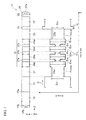
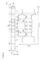
- Figures 3A to 3C show the configurations of semiconductor lasers of an Example according to embodiments of the present invention.
- Figures 4A to 4C show the band diagrams of the semiconductor lasers shown in Figs. 3 .
- FIG. 5 is a chart showing the flow of major steps for producing a semiconductor laser LD1.
- the production of the semiconductor laser LD1 shown in Fig. 3A will be described with reference to Fig. 5 .
- the semiconductor laser LD1 was produced by metal organic chemical vapor deposition.
- the sources were trimethylgallium (TMG), trimethylaluminum (TMA), trimethylindium (TMI), ammonia (NH 3 ), silane (SiH 4 ), and biscyclopentadienyl magnesium (CP 2 Mg).
- TMG trimethylgallium
- TMA trimethylaluminum
- TMI trimethylindium
- NH 3 ammonia
- SiH 4 silane
- CP 2 Mg biscyclopentadienyl magnesium
- a GaN wafer is prepared.
- the GaN wafer is composed of n-type GaN and has a main surface having an off angle of 0.3°.
- the GaN wafer was placed in an metal organic chemical vapor deposition reactor (hereinafter, referred to as the deposition reactor). Ammonia and hydrogen were fed to the deposition reactor and the GaN wafer was subjected to a heat-treatment step in an atmosphere containing these gases at 1050°C.
- an AlGaN cladding layer was grown on the GaN wafer at 1150°C.
- the AlGaN cladding layer is, for example, an n-type Al 0.04 Ga 0.96 N layer having a thickness of 2 ⁇ m.
- an InGaN optical guiding layer was grown on the AlGaN cladding layer at a film deposition temperature T G1 .
- the film deposition temperature T G1 is, for example, 840°C.
- the InGaN optical guiding layer is, for example, an undoped In 0.04 Ga 0.96 N layer having a thickness of 100 nm.
- the indium composition of this InGaN optical guiding layer is larger than the indium composition of InGaN barrier layers that will be grown later.
- the InGaN barrier layer was grown on the InGaN optical guiding layer at a film deposition temperature T B2 .
- the film deposition temperature T B2 is higher than the film deposition temperature T G1 in Example 1 and, for example, 860°C.
- the InGaN barrier layer is, for example, an undoped In 0.02 Ga 0.98 N layer having a thickness of 15 nm.
- an InGaN well layer was grown on the InGaN barrier layer at 800°C.
- the InGaN well layer is, for example, an undoped In 0.18 Ga 0.82 N layer having a thickness of 3 nm.
- an InGaN barrier layer was grown on the InGaN optical guiding layer at a film deposition temperature T B1 .
- the film deposition temperature T B1 is higher than the film deposition temperature T G1 and equal to the film deposition temperature T B2 in Example 1 and, for example, 860°C.
- the InGaN barrier layer is, for example, an undoped In 0.02 Ga 0.98 N layer having a thickness of 15 nm.
- an InGaN well layer was grown on the InGaN barrier layer at 800°C.
- an InGaN barrier layer was grown on the InGaN well layer at the film deposition temperature T B1 .
- an InGaN well layer was then grown on the InGaN barrier layer at 800°C.
- an InGaN barrier layer was grown on the InGaN well layer at a film deposition temperature T B3 .
- the film deposition temperature T B3 is higher than the film deposition temperature T G1 in Example 1 and, for example, 860°C.
- the InGaN barrier layer is, for example, an undoped In 0.02 Ga 0.98 N layer having a thickness of 15 nm.
- an InGaN active layer including the three well layers was produced.
- an InGaN optical guiding layer was grown on the InGaN active layer at a film deposition temperature T G2 lower than the temperature T B2 .
- the film deposition temperature T G2 is, for example, 840°C.
- the InGaN optical guiding layer is, for example, an undoped In 0.04 Ga 0.96 N layer having a thickness of 100 nm.
- the indium composition of this InGaN optical guiding layer is larger than the indium composition of the InGaN barrier layers. In the formation of an optical waveguide region, the higher the indium composition is, the lower the growth temperature is.
- the growth temperature (for example, 860°C) of a barrier layer is higher than the growth temperature (for example, 840°C) of a optical guiding layer, crystal quality can be restored upon the formation of the barrier layer. Since a well layer is formed on the barrier layer having restored crystal quality, the well layer also has good crystal quality.
- the growth temperature of the InGaN optical guiding layers in Example 1 is preferably 760°C or more.
- the growth temperature of the InGaN optical guiding layers is preferably 880°C or less.
- the growth temperature of the InGaN well layers in Example 1 is preferably 700°C or more.
- the growth temperature of the InGaN well layers is preferably 840°C or less.
- the growth temperature of the barrier layers in Example 1 is preferably 800°C or more.
- the growth temperature of the barrier layers is preferably 920°C or less.
- the growth temperature of the barrier layers is higher than the growth temperature of the optical guiding layers.
- the growth temperature of the optical guiding layers is higher than the growth temperature of the well layers.
- an AlGaN electron blocking layer was grown on the InGaN optical guiding layer at 1100°C.
- the AlGaN electron blocking layer is, for example, a p-type Al 0.12 Ga 0.88 N layer having a thickness of 20 nm.
- an AlGaN cladding layer was grown on the AlGaN electron blocking layer at 1100°C.
- the AlGaN cladding layer is, for example, a p-type Al 0.04 Ga 0.96 N layer having a thickness of 400 nm.
- a GaN contact layer was grown on the AlGaN cladding layer at 1100°C.
- the GaN contact layer has a thickness of, for example, 50 nm.
- an epitaxial wafer was produced. After the epitaxial wafer was taken out from the deposition reactor, at step S112, an insulation film was grown on the contact layer.
- the insulation film is composed of, for example, silicon oxide grown by a CVD method. A contact window having a width of 10 ⁇ m was formed.
- an anode electrode was formed on the contact window and the insulation layer.
- An anode electrode A is constituted by, for example, Ni/Au formed by vacuum deposition.
- a pad electrode was formed so as to be connected to the anode electrode.
- the pad electrode is constituted by, for example, Ti/Au formed by vacuum deposition.
- a cathode electrode was formed on the ground back surface.
- a cathode electrode K is constituted by, for example, Ti/Al formed by vacuum deposition.
- a pad electrode was formed so as to be connected to the cathode electrode.
- the pad electrode is constituted by, for example, Ti/Au formed by vacuum deposition.
- the substrate product was cleaved to produce laser bars.
- Each laser bar had cleaved surfaces CL1 and CL2 and had a cavity length of 800 ⁇ m.
- a gain-guided-type semiconductor laser was produced from the laser bar.
- optical guiding layers were composed of In 0.02 Ga 0.98 N and barrier layers were also composed of In 0.02 Ga 0.98 N.
- the optical guiding layers and the barrier layers were grown at a growth temperature of 860°C.
- optical guiding layers were composed of In 0.04 Ga 0.96 N and barrier layers were also composed of In 0.04 Ga 0.96 N.
- the optical guiding layers and the barrier layers were grown at a growth temperature of 840°C. Conditions other than the growth conditions of the optical guiding layers and the barrier layers were not changed.
- the semiconductor lasers LD1, LD2, and LD3 were operated by current injection. All the semiconductor lasers lased in the range of 430 nm or more to 440 nm.
- LD1 LD2 LD3 In composition of guiding layers 0.04 0.02 0.04 In composition of barrier layers 0.02 0.02 0.04 Threshold 550 mA 900 mA 600 mA
- the semiconductor laser LD1 of the working example exhibited the best characteristics.
- the semiconductor laser LD1 had the small threshold probably because the low In composition of the barrier layers enhanced the crystal quality of the light-emitting layer and use of the InGaN guiding layers having the high In composition resulted in a sufficiently good optical confinement property. There is a high probability that the crystal quality degrades after the InGaN well layers having the highest In composition are grown. However, the low In composition of the barrier layers and the high growth temperature of the barrier layers probably contribute to the restoration of the crystal quality.
- a semiconductor laser LD4 having a band diagram shown in Fig. 4D was produced.
- the semiconductor laser LD4 had an In composition gradient in the boundary between a optical guiding layer and a barrier layer. This composition gradient was achieved by continuously changing growth temperature.
- the composition gradient was formed in a region extending from the boundary of the optical guiding layer and the barrier layer to the optical guiding layer side by 10 nm and to the barrier layer side by 10 nm (in total, 20 nm).
- the semiconductor laser LD4 was produced as in Example 1.
- the semiconductor laser LD4 was operated by current injection and the lasing wavelength was 431 nm.
- LD1 LD4 composition gradient
- LD1 LD4 composition gradient
- LD1 LD4 composition gradient
- LD1 LD4 composition gradient
- guiding layers 0.04 0.04
- barrier layers 0.02 0.02
- the semiconductor laser LD4 had the threshold smaller than that of the semiconductor laser LD1. This is probably because the composition gradient improved the injection efficiency of carriers into the active layer.
- the electroluminescence (EL) spectra of the substrate products of the semiconductor lasers LD 1 and LD4 were measured.
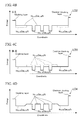
- Figures 6A and 6B show the measurement results of the EL spectra. Referring to Fig. 6A , two EL peaks at about the wavelengths of 380 nm and 420 nm were observed for the substrate product of the semiconductor laser LD1. Referring to Fig. 6B , a single EL peak at about the wavelength of 430 nm was observed for the substrate product of the semiconductor laser LD4. The two peaks in the EL spectrum probably show that carriers are accumulated in the guiding layers in the semiconductor laser LD 1. The single peak in the EL spectrum probably shows that the injection efficiency of carriers from the guiding layers into the active layer has been enhanced in the semiconductor laser LD 4.
- Figure 7 is a schematic view showing the configuration of a group III nitride semiconductor laser according to an embodiment of the present invention.
- an active layer 19b includes second and third barrier layers 39c and 41c.
- the second barrier layer 39c includes a portion having a band gap smaller than the band gap of a first InGaN region 21a.
- the indium composition of the entire of the second barrier layer 39c is smaller than the indium composition of the first InGaN region 21a.
- this group III nitride semiconductor laser carriers smoothly flow from a optical guiding layer 21 to a well layer 27a.
- the third barrier layer 41c includes a portion having a band gap smaller than the band gap of a second InGaN region 23a.
- the indium composition of the entire of the third barrier layer 41c is smaller than the indium composition of the second InGaN region 23a.
- this group III nitride semiconductor laser carriers smoothly flow from a optical guiding layer 23 to a well layer 27c.
- the first optical guiding layer 21 may include an eighth InGaN region 21c as in the group III nitride semiconductor laser 11a.
- the eighth InGaN region 21c is provided between the first InGaN region 21a and an n-type cladding layer 15.
- the eighth InGaN region 21c has an indium composition that decreases in the direction from the first InGaN region 21a to the n-type cladding layer 15. Since the eighth InGaN region 21c is close to the cladding layer 15, a decrease in the indium composition of the eighth InGaN region 21c results in only a small decrease in the optical confinement property. On the other hand, a decrease in the indium composition of the eighth InGaN region 21c can reduce degradation of the crystal quality of the optical guiding layer 21.
- the second optical guiding layer 23 preferably includes a seventh InGaN region 23c as in the group III nitride semiconductor laser 11a.
- the distribution of refractive index of the second optical guiding layer 23 can be matched with the distribution of refractive index of the first optical guiding layer 21.
- the seventh InGaN region 23c has an indium composition that decreases from the second InGaN region 23a toward the p-type cladding layer 17. Since the seventh InGaN region is close to the cladding layer, a decrease in the indium composition of the seventh InGaN region results in only a small decrease in the optical confinement property.
- a semiconductor laser LD5 was produced in a manner similar to that in Example 1.
- the first and second optical guiding layers had an indium composition of 0.04.
- the second and third barrier layers had an indium composition of 0.05.
- the second and third barrier layers had a thickness of 15 nm.
- the growth temperature of the second and third barrier layers was 830°C.
- the threshold of the semiconductor laser LD5 was low and almost equal to that in Example 2. According to the measurement result of EL spectrum, the peak derived from the optical guiding layers was extremely small.
- accumulation of carriers in the optical guiding layers is avoided as with the semiconductor laser in Example 2 and carrier injection efficiency is enhanced.
- the light-emitting characteristics of the semiconductor laser LD5 are better than the light-emitting characteristics of the semiconductor lasers LD2 and 3. This is probably because the small In composition of the inner two barrier layers allowed an increase in the growth temperature of these barrier layers and, as a result, the crystal quality was restored.
- the second barrier layer 39c may have an In composition gradient in which the In composition gradually increases in the direction from the optical guiding layer 21 to the well layer 27a.
- the second barrier layer 39c and the optical guiding layer 21 may have an In composition gradient in which the In composition gradually increases in the direction from the n-type cladding layer 15 to the well layer 27a.
- the third barrier layer 41c may have an In composition gradient in which the In composition gradually increases in the direction from the optical guiding layer 23 to the well layer 27c.
- the third barrier layer 41c and the optical guiding layer 23 may have an In composition gradient in which the In composition gradually increases in the direction from the p-type cladding layer 17 to the well layer 27c.
- the InGaN region 21a having an indium composition of 0.03 or more can impart a high refractive index to the optical guiding layer 21.
- the InGaN region 21a having an indium composition of more than 0.12 degrades the crystal quality of the optical guiding layer 21.
- the InGaN region 23a having an indium composition of 0.03 or more can impart a high refractive index to the optical guiding layer 23.
- the InGaN region 23a having an indium composition of more than 0.12 degrades the crystal quality of the optical guiding layer 23.
- the first optical guiding layer 21 preferably has a thickness of 150 nm or less.
- the second optical guiding layer 23 preferably has a thickness of 150 nm or less.
- the first optical guiding layer 21 preferably has a thickness of 25 nm or more.
- the second optical guiding layer 23 preferably has a thickness of 25 nm or more. The far-field pattern of a semiconductor laser can be adjusted by adjusting the thickness of the first optical guiding layer 21 and the second optical guiding layer 23.
- FIG 8 shows the configuration of an epitaxial wafer in which cathodoluminescence is measured.
- an epitaxial wafer E does not include a p-side InGaN optical guiding layer or a p-type cladding layer.
- a GaN wafer having a main surface that is off 2° in the direction of the a-axis and a GaN wafer having a main surface that is exactly conform to the c-plane were prepared. Epitaxial growth was conducted on these wafers.
- Figures 9A and 9B show cathodoluminescence (CL) images. Referring to Fig.
- a CL image having an island pattern was observed. This image shows that a multiple quantum well structure was grown to have an island pattern.
- Fig. 9B a CL image having a streak pattern was observed. This image shows that a multiple quantum well structure was formed by step-flow growth. As the off angle increases, the step density increases. Thus, growth in an island pattern is suppressed.
- the off angle of a main surface of a wafer composed of a group III nitride semiconductor such as GaN or InGaN is preferably inclined at an angle of 1° or more with respect to the c-plane of the group III nitride semiconductor and is preferably inclined at an angle of 50° or less with respect to the c-plane of the group III nitride semiconductor.
- a surface inclined with respect to the c-plane is suitable for growing InGaN having a high indium composition.
- an off angle of 10° or more can result in a reduction in a piezoelectric field.
- the direction in which a main surface of a wafer is inclined can be the a-axis direction of a group III nitride semiconductor.
- a resonator can be produced by m-plane cleavage.
- GaN wafers having off angles of 2°, 20°, and 40° in the direction of the a-axis were prepared.
- the same laser structures as in Example 1 were produced on these GaN wafers.
- Laser waveguides were formed in the direction of the m-axis.
- electrodes were formed, cleavage along the m-plane was conducted to produce laser bars.
- Off angle Threshold current 0.3° 550 mA (Example 1) 2° 500 mA 20° 550 mA 40° 550 mA
- the semiconductor laser produced on the GaN wafer having an off angle of 2° had a threshold current of about 500 mA, which is lower than that in Example 1. This is probably because the step-flow growth improved crystal quality and surface flatness.
- the semiconductor lasers produced on the GaN wafers having off angles of 20° and 40° had a threshold current equal to or slightly higher than that in Example 1.
- a threshold current equal to or slightly higher than that in Example 1.
- an off angle is large, incorporation of indium is suppressed in the growth of an InGaN layer. For this reason, a decrease in the growth temperature of InGaN was required.
- the threshold current is substantially equal to that in Example 1. Wafers having these off angles have a small piezoelectric field and hence a blue shift until lasing is smaller than that in Example 1.
- the group III nitride semiconductor lasers 11, 11a, and 11b can be produced from high quality GaN wafers having a threading dislocation density of 10 6 cm -2 or less.
- the semiconductor lasers can be produced from GaN wafers having a diameter of 45 mm or more.
- Substrates for the group III nitride semiconductor lasers 11, 11a, and 11b can be composed of InGaN.
- the lattice mismatch between a optical guiding layer having a large indium composition and a substrate can be reduced.
- An InGaN substrate having an off angle of 2° in the direction of the a-axis was prepared.
- the InGaN substrate is composed of In 0.05 G 0.95 N.
- An epitaxial wafer for a laser structure was formed on this InGaN substrate as described below.
- the InGaN substrate was placed in a deposition reactor. While nitrogen is fed into the deposition reactor, the temperature of the InGaN substrate was increased to 800°C.
- An AlGaN layer was grown on the InGaN substrate.
- the AlGaN layer is composed of n-type Al 0 . 02 Ga 0.98 N and has a thickness of, for example, 10 nm.
- the growth temperature of AlGaN is, for example, 800°C.
- the n-type cladding layer is composed of, for example, Si-doped GaN and has a thickness of, for example, 2 ⁇ m.
- the growth temperature of GaN is, for example, 1100°C.
- a optical guiding layer was grown on the n-type cladding layer.
- the optical guiding layer is composed of, for example, undoped In 0.08 Ga 0.92 N and has a thickness of, for example, 100 nm.
- the active layer includes, for example, well layers composed of InGaN and barrier layers composed of InGaN.
- the well layers are composed of In 0.30 Ga 0.70 N and have a thickness of 2 nm.
- the barrier layers are composed of In 0.05 Ga 0.95 N and have a thickness of 15 nm.
- the active layer includes three well layers.
- the growth temperature of the well layers is, for example, 770°C.
- the growth temperature of the barrier layers is, for example, 830°C.
- a optical guiding layer was grown on the active layer.
- the optical guiding layer is composed of, for example, undoped In 0.08 Ga 0.92 N, and has a thickness of, for example, 100 nm.
- the growth temperature of the optical guiding layer is, for example, 800°C.
- An electron blocking layer was grown on the optical guiding layer.
- the electron blocking layer is composed of, for example, Mg-doped p-type Al 0.10 Ga 0.90 N, and has a thickness of, for example, 20 nm.
- the growth temperature of the electron blocking layer is, for example, 1100°C.
- a p-type cladding layer was grown on the electron blocking layer.
- the p-type cladding layer is composed of, for example, Mg-doped Al 0 .
- the growth temperature of GaN is, for example, 1100°C.
- a p-type contact layer was grown on the p-type cladding layer.
- the p-type contact layer is composed of, for example, Mg-doped GaN, and has a thickness of, for example, 50 nm.
- the growth temperature of GaN is, for example, 1100°C.
- An epitaxial wafer was produced by producing a laser structure similar to that of the semiconductor laser LD6 on a GaN substrate having an off angle of 2°.
- a semiconductor laser LD7 was produced from this epitaxial wafer.
- the semiconductor lasers LD6 and LD7 lased.
- the lasing wavelength was 470 to 480 nm.
- the thresholds of the semiconductor lasers LD6 and LD7 were respectively about 1500 mA and about 1700 mA. Since the semiconductor laser LD6 was produced on the InGaN substrate, the occurrence of strain or defects due to the lattice mismatch between the substrate and the epitaxial films is reduced even when the InGaN thick films having In compositions of several percent were grown. This is probably a cause that the threshold was reduced.
- a nitride semiconductor laser diode emitting light at a long lasing wavelength of 430 nm or more has been demanded.
- the difference in refractive index between the cladding layer and the guiding layer becomes small.
- a technique is required with which optical confinement is enhanced compared with blue-violet laser (wavelength: about 405 nm) used for Blu-ray or HD-DVD.
- InGaN is used as a material for barrier layers and guiding layers, and the In compositions of the barrier layers and the guiding layers are increased.
- An epitaxial wafer of a semiconductor laser includes multilayered epitaxial films.
- a nitride semiconductor laser diode according to the present invention has high InGaN proportion in this multilayer structure.
- the crystal quality of the epitaxial films degrades. Such degradation of the crystal quality tends to occur after a well layer having a high In composition is grown.
- the In composition of barrier layers sandwiching well layers is reduced. This reduction decreases the average refractive index of the waveguide.
- the In composition of optical guiding layers is increased. Optical confinement can be maintained and the crystal quality of a multiple quantum well structure can be improved.
- the barrier layers having a low In composition are grown, the crystal quality is restored. Since the optical guiding layers have a high refractive index, a desired optical confinement is provided.
- the optical guiding layers in part have an In composition gradient.
- a reduction in carrier injection efficiency can be avoided even when optical guiding layers having a high In composition are used.
- the In composition gradient of the optical guiding layers can result in the avoidance of accumulation of carriers in optical guiding layers having a high In composition.
- a free-standing GaN wafer having an off angle is used.
- the probability of occurrence of degradation of crystal quality is low even when an InGaN region is thick.
- a surface morphology in an island pattern tends to be generated.
- Use of a GaN substrate having a large off angle increases the step density of a main surface of the substrate. Thus, the surface morphology in an island pattern is suppressed.
Landscapes
- Physics & Mathematics (AREA)
- Optics & Photonics (AREA)
- Condensed Matter Physics & Semiconductors (AREA)
- General Physics & Mathematics (AREA)
- Electromagnetism (AREA)
- Chemical & Material Sciences (AREA)
- Engineering & Computer Science (AREA)
- Nanotechnology (AREA)
- Life Sciences & Earth Sciences (AREA)
- Biophysics (AREA)
- Crystallography & Structural Chemistry (AREA)
- Semiconductor Lasers (AREA)
Abstract
A group III nitride semiconductor laser is provided that has a good optical confinement property and includes an InGaN well layer having good crystal quality.
An active layer 19 is provided between a first optical guiding layer 21 and a second optical guiding layer 23. The active layer 19 can include well layers 27a, 27b, and 27c and further includes at least one first barrier layer 29a provided between the well layers. The first and second optical guiding layers 21 and 23 respectively include first and second InGaN regions 21a and 23 a smaller than the band gap E29 of the first barrier layer 29a, and hence the average refractive index nGUIDE of the first and second optical guiding layers 21 and 23 can be made larger than the refractive index n29 of the first barrier layer 29a. Thus, good optical confinement is achieved. The band gap E29 of the first barrier layer 29a is larger than the band gaps E21 and E23 of the first and second InGaN regions 21a and 23a.
Description
- The present invention relates to a group III nitride semiconductor laser.
- Non-Patent
Document 1 describes a blue laser diode formed on a nonpolar m-plane gallium nitride substrate. The lasing wavelength is 451.8 nm and the threshold current is 134 mA. The laser diode includes an InGaN quantum well structure, a p-type GaN or InGaN optical guiding layer, an n-type GaN or InGaN optical guiding layer, and an Al-containing cladding layer. -
Patent Document 1 describes an AlGaInN-based edge emitting semiconductor laser device. The semiconductor laser device is fabricated on a sapphire substrate. A GaInN-ELO structure layer is formed on the sapphire substrate and a stacked layer structure is grown on the structure layer by MOCVD. The st acked layer structure is constituted by an n-GaInN contact layer, an n-AlGaInN cladding layer, an n-GaN optical guiding layer, a GaInN active layer, a p-GaN optical guiding layer, a p-(GaN:Mg/AlGaInN) cladding layer, and a p-GaInN contact layer.
Patent Document 2 describes a light-emitting device employing a sapphire substrate. The light-emitting device includes a first intermediate layer composed of In0.08Ga0.92N, a second intermediate layer composed of In0.15Ga0.85N, and a light-emitting layer composed of In0.20Ga0.80N.
Patent Document 3 describes a group III nitride-based compound semiconductor light-emitting device. This light-emitting device includes an In0.03Ga0.97N intermediate layer, an n-type cladding layer, and a light-emitting layer. The n-type cladding layer is positioned between the intermediate layer and the light-emitting layer. The light-emitting layer includes a GaN barrier layer and an In0.20Ga0.80N well layer. - [Non-Patent Document 1] JJAP, vol. 46, No. 35, 2007, p. L820-L822
- [Patent Document 1] Japanese Unexamined Patent Application Publication No.
2003-332697 - [Patent Document 2] Japanese Unexamined Patent Application Publication No.
9-266327 - [Patent Document 3] Japanese Unexamined Patent Application Publication No.
2000-286448 - The light-emitting device of
Patent Document 1 includes GaN optical guiding layers. The light-emitting devices ofPatent Documents Non-Patent Document 1, a semiconductor laser having a lasing wavelength of 450 nm is fabricated on an m-plane GaN substrate. When an active layer is formed so as to obtain a longer lasing wavelength, the difference in refractive index between a cladding layer and a guiding layer becomes small. To avoid this, an InGaN guiding layer is used instead of a GaN guiding layer. Thus, an optical confinement property is enhanced. InPatent Document 1, InGaN well layers and InGaN barrier layers are used and optical guiding layers are composed of GaN. - Use of InGaN optical guiding layers instead of GaN optical guiding layers can provide higher refractive indices of an active layer and neighboring optical guiding layers than the refractive indices of cladding layers. Thus, an optical confinement property is enhanced.
- However, many InGaN layers having In compositions of several percent are grown between an n-type cladding layer and a p-type cladding layer. The growth temperature of InGaN is lower than the growth temperatures of GaN and AlGaN. For this reason, there is a high probability of three-dimensional growth in the growth of InGaN compared with the growth of GaN and AlGaN. In the growth of InGaN to a large thickness, the larger the thickness is, the poorer the crystal quality becomes. An InGaN layer having a higher composition of indium is required to be grown at a lower growth temperature. Low growth temperature results in poor InGaN crystal quality. Thus, InGaN well layers have poor crystal quality.
- The present invention has been accomplished under these circumstances and an object of the present invention is to provide a group III nitride semiconductor laser that has a good optical confinement property and includes an InGaN well layer having good crystal quality.
- A group III nitride semiconductor laser according to an aspect of the present invention includes: (a) a substrate having a main surface; (b) an n-type cladding layer provided on the substrate and composed of a group III nitride semiconductor; (c) a p-type cladding layer provided on the substrate and composed of a group III nitride semiconductor; (d) an active layer provided between the n-type cladding layer and the p-type cladding layer; (e) a first optical guiding layer provided between the n-type cladding layer and the active layer; and (f) a second optical guiding layer provided between the p-type cladding layer and the active layer. The active layer includes a plurality of well layers and at least one first barrier layer provided between the well layers; the first optical guiding layer includes a first InGaN region composed of InGaN that has a band gap smaller than a band gap of the first barrier layer and larger than a band gap of the well layers; the second optical guiding layer includes a second InGaN region that is composed of InGaN; among the well layers of the active layer, a well layer that is closest to the first optical guiding layer is a first well layer; among the well layers of the active layer, a well layer that is closest to the second optical guiding layer is a second well layer; and the active layer includes a second barrier layer provided between the first well layer and the first optical guiding layer, and a third barrier layer provided between the second well layer and the second optical guiding layer.
- In this group III nitride semiconductor laser, since the first optical guiding layer includes the first InGaN region smaller in band gap than the first barrier layer, the average refractive index of the first optical guiding layer can be made larger than the refractive index of the first barrier layer. Thus, good optical confinement is achieved. The band gap of the first barrier layer is larger than the band gap of the first InGaN region. For this reason, the growth temperature of the first barrier layer can be made higher than the growth temperature of the first optical guiding layer, and hence the first barrier layer can be made to have good crystal quality. Thus, the well layer on the first barrier layer has good crystal quality.
- In a group III nitride semiconductor laser according to the present invention, the second InGaN region preferably has a band gap smaller than the band gap of the first barrier layer and larger than the band gap of the first and second well layers. In this group III nitride semiconductor laser, since the second optical guiding layer includes the second InGaN region smaller in band gap than the first barrier layer, the average refractive index of the second optical guiding layer can be made larger than the refractive index of the first barrier layer. Thus, good optical confinement is achieved.
- In a group III nitride semiconductor laser according to the present invention, the second barrier layer may include a portion having a band gap larger than the band gap of the first InGaN region; and the third barrier layer may include a portion having a band gap larger than a band gap of the second InGaN region. In this group III nitride semiconductor laser, since the band gaps of the first to third barrier layers are larger than the band gaps of the first and second InGaN regions, the growth temperatures of the first to third barrier layers can be made higher than the growth temperatures of the first and second InGaN regions, and hence the first to third barrier layers can be made to have good crystal quality. Thus, the well layers on the first to third barrier layers have good crystal quality.
- In a group III nitride semiconductor laser according to the present invention, the first barrier layer may be composed of a gallium nitride-based semiconductor, and the second and third barrier layers may be composed of the gallium nitride-based semiconductor.
- In this group III nitride semiconductor laser, since the band gaps of the second and third barrier layers are the same as the band gap of the first barrier layer, the second and third barrier layers have good crystal quality. Although InGaN having a high indium composition is used for the optical guiding layers, the crystal quality can be improved in the growth of the barrier layers.
- In a group III nitride semiconductor laser according to the present invention, the second optical guiding layer may further include a third InGaN region provided between the third barrier layer and the second InGaN region, and the third InGaN region may have an indium composition that increases in a direction from the third barrier layer to the second InGaN region.
- In this group III nitride semiconductor laser, accumulation of holes in the second optical guiding layer can be reduced.
- In a group III nitride semiconductor laser according to the present invention, the third barrier layer may include an InGaN region, and the InGaN region of the third barrier layer may have an indium composition that increases in a direction from the second well layer to the second InGaN region.
- In this group III nitride semiconductor laser, the third barrier layer includes at least one portion having a composition gradient. As a result, a stepwise potential barrier against holes flowing from the second optical guiding layer to the well layers is reduced.
- In a group III nitride semiconductor laser according to the present invention, the second optical guiding layer may further include a fourth InGaN region provided between the second InGaN region and the p-type cladding layer, and the fourth InGaN region may have an indium composition that decreases from the second InGaN region toward the p-type cladding layer.
- In this group III nitride semiconductor laser, since the fourth InGaN region of the optical guiding layer is close to the cladding layer, a decrease in the indium composition of the fourth InGaN region results in only a small decrease in the optical confinement property. On the other hand, a decrease in the indium composition of the fourth InGaN region can reduce degradation of the crystal quality of the optical guiding layer.
- In a group III nitride semiconductor laser according to the present invention, the first optical guiding layer may further include a fifth InGaN region provided between the second barrier layer and the first InGaN region, and the fifth InGaN region may have an indium composition that increases in a direction from the second barrier layer to the first InGaN region.
- In this group III nitride semiconductor laser, accumulation of electrons in the first optical guiding layer can be reduced.
- In a group III nitride semiconductor laser according to the present invention, the second barrier layer may include an InGaN region, and the InGaN region of the second barrier layer may have an indium composition that increases in a direction from the first well layer to the first InGaN region.
- In this group III nitride semiconductor laser, the second barrier layer includes at least one portion having a composition gradient. As a result, a stepwise potential barrier against electrons flowing from the first optical guiding layer to the well layers is reduced.
- In a group III nitride semiconductor laser according to the present invention, the first optical guiding layer may further include a sixth InGaN region provided between the first InGaN region and the n-type cladding layer, and the sixth InGaN region may have an indium composition that decreases in a direction from the first InGaN region to the n-type cladding layer.
- In this group III nitride semiconductor laser, since the sixth InGaN region of the optical guiding layer is close to the cladding layer, a decrease in the indium composition of the sixth InGaN region results in only a small decrease in the optical confinement property. On the other hand, a decrease in the indium composition of the sixth InGaN region can reduce degradation of the crystal quality of the optical guiding layer.
- In a group III nitride semiconductor laser according to the present invention, the second barrier layer includes a portion having a band gap smaller than the band gap of the first InGaN region; and the third barrier layer includes a portion having a band gap smaller than a band gap of the second InGaN region.
- In this group III nitride semiconductor laser, carriers smoothly flow from the optical guiding layers to the well layers.
- In a group III nitride semiconductor laser according to the present invention, the second optical guiding layer may further include a seventh InGaN region provided between the second InGaN region and the p-type cladding layer, and the seventh InGaN region may have an indium composition that decreases from the second InGaN region toward the p-type cladding layer.
- In this group III nitride semiconductor laser, since the seventh InGaN region of the optical guiding layer is close to the cladding layer, a decrease in the indium composition of the seventh InGaN region results in only a small decrease in the optical confinement property. On the other hand, a decrease in the indium composition of the seventh InGaN region can reduce degradation of the crystal quality of the optical guiding layer.
- In a group III nitride semiconductor laser according to the present invention, the first optical guiding layer may further include an eighth InGaN region provided between the first InGaN region and the n-type cladding layer, and the eighth InGaN region may have an indium composition that decreases in a direction from the first InGaN region to the n-type cladding layer.
- In this group III nitride semiconductor laser, since the eighth InGaN region of the optical guiding layer is close to the cladding layer, a decrease in the indium composition of the eighth InGaN region results in only a small decrease in the optical confinement property. On the other hand, a decrease in the indium composition of the eighth InGaN region can reduce degradation of the crystal quality of the optical guiding layer.
- In a group III nitride semiconductor laser according to the present invention, the active layer may include a multiple quantum well structure provided such that the group III nitride semiconductor laser has a light-emitting wavelength in a wavelength region of 430 nm or more.
- This group III nitride semiconductor laser is suitable as a semiconductor laser for long wavelengths in which a material having a high indium composition is used for well layers.
- In a group III nitride semiconductor laser according to the present invention, the first optical guiding layer may have a thickness of 150 nm or less, and the second optical guiding layer may have a thickness of 150 nm or less. According to this group III nitride semiconductor laser, when a optical guiding layer having a high indium composition has a thickness of more than 150 nm, the restoration of crystal quality in the growth of the active layer is not sufficiently achieved. As a result, the crystal quality of the active layer is degraded.
- In a group III nitride semiconductor laser according to the present invention, the first InGaN region of the first optical guiding layer may have an indium composition of 0.03 or more. In this group III nitride semiconductor laser, the InGaN region having an indium composition of 0.03 or more can impart a high refractive index to the optical guiding layer. The second InGaN region of the second optical guiding layer may have an indium composition of 0.03 or more. In this group III nitride semiconductor laser, the InGaN region having an indium composition of 0.03 or more can impart a high refractive index to the optical guiding layer.
- In a group III nitride semiconductor laser according to the present invention, the first optical guiding layer may have an indium composition of 0.12 or less. According to this group III nitride semiconductor laser, an InGaN region having an indium composition of more than 0.12 degrades the crystal quality of the optical guiding layer.
- In a group III nitride semiconductor laser according to the present invention, the second optical guiding layer may have an indium composition of 0.12 or less. According to this group III nitride semiconductor laser, an InGaN region having an indium composition of more than 0.12 degrades the crystal quality of the optical guiding layer.
- In a group III nitride semiconductor laser according to the present invention, the substrate may be composed of a group III nitride semiconductor, the main surface of the substrate may be inclined at an angle of 1° or more with respect to a c-plane of the group III nitride semiconductor, and the main surface of the substrate may be inclined at an angle of 50° or less with respect to the c-plane of the group III nitride semiconductor. According to this group III nitride semiconductor laser, such a surface inclined with respect to the c-plane is suitable for growing InGaN having a high indium composition.
- In a group III nitride semiconductor laser according to the present invention, the main surface may be inclined in a direction of an a-axis of the group III nitride semiconductor. A resonator can be produced from this group III nitride semiconductor laser by m-plane cleavage.
- In a group III nitride semiconductor laser according to the present invention, the substrate may be composed of GaN. According to this group III nitride semiconductor laser, a semiconductor laser can be produced with a high quality GaN wafer.
- In a group III nitride semiconductor laser according to the present invention, the substrate may be composed of InGaN. According to this group III nitride semiconductor laser, the lattice mismatch between a optical guiding layer having a large indium composition and a substrate can be reduced.
- A method for producing a group III nitride semiconductor laser according to the present invention includes: (a) a step of growing a first InGaN optical guiding layer on a first-conductivity-type cladding layer at a first temperature; (b) a step of growing a barrier layer after the first InGaN optical guiding layer is grown; (c) a step of growing an InGaN well layer after the barrier layer is grown; (d) a step of growing another barrier layer at a second temperature after the InGaN well layer is grown; (e) a step of growing another InGaN well layer after the another barrier layer is grown; (f) a step of growing still another barrier layer after the another InGaN well layer is grown; and (g) a step of growing a second InGaN optical guiding layer at a third temperature after the still another barrier layer is grown. The second temperature is higher than the first and third temperatures.
- According to this method, since the second temperature is higher than the first and third temperatures, crystal quality is enhanced in the growth of the another barrier layer. Thus, degradation of the crystal quality of the well layer grown on this another barrier layer can be avoided.
- The above-described object, another object, features, and advantages of the present invention will more readily become apparent from the following detailed description of preferred embodiments of the present invention with reference to attached drawings. Advantages
- As described above, the present invention provides a group III nitride semiconductor laser that has a good optical confinement property and includes an InGaN well layer having good crystal quality.
-
- [
Fig. 1] Figure 1 is a schematic view showing the configuration of a group III nitride semiconductor laser according to an embodiment of the present invention. - [
Fig. 2] Figure 2 is a schematic view showing the configuration of a group III nitride semiconductor laser according to another embodiment of the present invention. - [
Fig. 3A] Figure 3A shows the configuration of a semiconductor laser of an Example according to an embodiment of the present invention. - [
Fig. 3B] Figure 3B shows the configuration of a semiconductor laser of an Example according to an embodiment of the present invention. - [
Fig. 3C] Figure 3C shows the configuration of a semiconductor laser of an Example according to an embodiment of the present invention. - [
Fig. 4A] Figure 4A shows the band diagram of a semiconductor laser. - [
Fig. 4B] Figure 4B shows the band diagram of a semiconductor laser. - [
Fig. 4C] Figure 4C shows the band diagram of a semiconductor laser. - [
Fig. 4D] Figure 4D shows the band diagram of a semiconductor laser. - [
Fig. 5] Figure 5 is a chart showing the flow of steps according to an Example. - [
Fig. 6A] Figure 6A shows the measurement result of electroluminescence. - [
Fig. 6B] Figure 6B shows the measurement result of electroluminescence. - [
Fig. 7] Figure 7 is a schematic view showing the configuration of a group III nitride semiconductor laser according to an embodiment of the present invention. - [
Fig. 8] Figure 8 shows the configuration of an epitaxial wafer in which cathodoluminescence is measured. - [
Fig. 9A] Figure 9A shows a cathodoluminescence image. - [
Fig. 9B] Figure 9B shows a cathodoluminescence image. -
- 11, 11a, 11b
- group III nitride semiconductor lasers
- 13
- substrate
- 13a
- main surface of substrate
- 13b
- back surface of substrate
- 15
- n-type cladding layer
- 17
- p-type cladding layer
- 19
- active layer
- 21
- first optical guiding layer
- 21a
- first InGaN region
- 21b
- fifth InGaN region
- 21c
- sixth InGaN region
- 23
- second optical guiding layer
- 23a
- second InGaN region
- 23b
- third InGaN region
- 23c
- fourth InGaN region
- 27a, 27b, 27c
- well layers
- 29a
- first barrier layer
- 31
- electron blocking layer
- 33
- p-type contact layer
- 35
- insulation film
- 37a, 37b
- electrodes
- 39a, 39b
- second barrier layers
- 40a
- first portion of second barrier layer
- 40b
- second portion of second barrier layer
- 41a, 41b
- third barrier layers
- 42a
- first portion of third barrier layer
- 42b
- second portion of third barrier layer
- G
- electrons
- H
- holes
- The findings of the present invention can be readily understood in consideration of the following detailed description with reference to the attached drawings serving as examples. Hereinafter, embodiments of a group III nitride semiconductor laser according to the present invention are described with reference to the attached drawings. Where possible, like reference numerals are used to denote like elements.
-
Figure 1 is a schematic view showing the configuration of a group III nitride semiconductor laser according to an embodiment of the present invention. A group IIInitride semiconductor laser 11 includes asubstrate 13, an n-type cladding layer 15, a p-type cladding layer 17, anactive layer 19, a firstoptical guiding layer 21, and a second optical guidinglayer 23. Thesubstrate 13 includes amain surface 13a and aback surface 13b. Thesubstrate 13 may be composed of, for example, a gallium nitride-based semiconductor. The n-type cladding layer 15 is provided on themain surface 13a of thesubstrate 13 and composed of a group III nitride semiconductor. The p-type cladding layer 17 is provided on themain surface 13a of thesubstrate 13 and also composed of a group III nitride semiconductor. Theactive layer 19 is provided between the n-type cladding layer 15 and the p-type cladding layer 17. The firstoptical guiding layer 21 is provided between the n-type cladding layer 15 and theactive layer 19. The second optical guidinglayer 23 is provided between the p-type cladding layer 17 and theactive layer 19. Theactive layer 19 is provided between the firstoptical guiding layer 21 and the second optical guidinglayer 23. Theactive layer 19 can include a plurality of well layers (for example, 27a, 27b, and 27c) and also includes at least onefirst barrier layer 29a provided between these well layers. The firstoptical guiding layer 21 includes afirst InGaN region 21a. Thefirst InGaN region 21a is composed of InYGa1-YN (0 < Y < 1) and has a band gap E21. The band gap E21 is smaller than the band gap E29 of thefirst barrier layer 29a and larger than the band gap EW of the well layers (for example, 27a, 27b, and 27c). The second optical guidinglayer 23 includes asecond InGaN region 23a. Thesecond InGaN region 23a is composed of InZGa1-ZN (0 < Z < 1) and has a band gap E23. The band gap E23 is smaller than the band gap E29 of thefirst barrier layer 29a and larger than the band gap EW of the well layers (for example, 27a, 27b, and 27c). - In the group III
nitride semiconductor laser 11, the first and second optical guidinglayers second InGaN regions first barrier layer 29a, and hence the average refractive index nGUIDE of the first and second optical guidinglayers first barrier layer 29a. Thus, good optical confinement is achieved. Since the band gap E29 of thefirst barrier layer 29a is larger than the band gaps E21 and E23 of the first andsecond InGaN regions first barrier layer 29a can be made higher than the growth temperatures of the first andsecond InGaN regions first barrier layer 29a can be made to have good crystal quality, and hence the well layer on thefirst barrier layer 29a has good crystal quality. The indium composition of either one of the first and second optical guidinglayers first barrier layer 29a. - The n-
type cladding layer 15 can be composed of, for example, AlGaN, GaN, InAlGaN, or the like. The p-type cladding layer 17 can be composed of, for example, AlGaN, GaN, InAlGaN, or the like. Thebarrier layer 29a can be composed of, for example, InGaN, GaN, AlGaN, or the like. Thewell layer 27a can be composed of, for example, InGaN. The firstoptical guiding layer 21 can include an undoped InGaN region. The second optical guidinglayer 23 can include an undoped InGaN region. Such undoped semiconductor can reduce light absorption by carriers. - The group III
nitride semiconductor laser 11 includes a p-type contact layer 33 provided on the p-type cladding layer 17. The p-type contact layer 33 is connected to anelectrode 37a (for example, an anode) via an opening of aninsulation film 35. When thesubstrate 13 is conductive, anelectrode 37b (for example, a cathode) is formed on theback surface 13b of thesubstrate 13. - The group III
nitride semiconductor laser 11 according to the present embodiment can include anelectron blocking layer 31 between theoptical guiding layer 23 and the p-type cladding layer 17. Theelectron blocking layer 31 has a band gap larger than that of thecladding layer 17. Theelectron blocking layer 31 can be composed of, for example, AlGaN, InAlGaN, or the like. Thecontact layer 33 can be composed of, for example, GaN, AlGaN, InGaN, InAlGaN, or the like. - In the group III
nitride semiconductor laser 11, thefirst well layer 27a among the well layers (27a, 27b, and 27c) of theactive layer 19 is the closest to the firstoptical guiding layer 21. Thesecond well layer 27c among the well layers (27a, 27b, and 27c) of theactive layer 19 is the closest to the second optical guidinglayer 23. Theactive layer 19 includes asecond barrier layer 39a and athird barrier layer 41a. Thesecond barrier layer 39a is provided between thefirst well layer 27a and the firstoptical guiding layer 21. Thethird barrier layer 41a is provided between thesecond well layer 27c and the second optical guidinglayer 23. The band gap E39a of thesecond barrier layer 39a is larger than the band gap E21 of thefirst InGaN region 21a. The band gap E41a of thethird barrier layer 41a is larger than the band gap E23 of thesecond InGaN region 23a. - In the group III
nitride semiconductor laser 11, since the band gaps of the first tothird barrier layers second InGaN regions third barrier layers second InGaN regions third barrier layers third barrier layers - Electrons G are fed from the n-
type cladding layer 15 through theoptical guiding layer 21 to theactive layer 19. Holes H are fed from the p-type cladding layer through theoptical guiding layer 23 to theactive layer 19. In theactive layer 19, the electrons and the holes are recombined to produce light. The produced light is confined in a waveguide region (21, 19, and 23). Since the band gaps E21 and E23 of theInGaN regions barrier layer 29a, the difference between the refractive indices of the cladding layers 15 and 17 and the refractive indices of the optical guiding layers 21 and 23 can be increased to thereby provide a desired difference between the refractive indices. Since the indium compositions of theInGaN regions InGaN regions barrier layer 29a can be grown at a temperature higher than the growth temperatures for theInGaN regions active layer 19 can be made to have crystal quality better than that of theInGaN regions - In the group III
nitride semiconductor laser 11, the second and third barrier layers 39a and 41a may be composed of substantially the same gallium nitride-based semiconductor as in thefirst barrier layer 29a. Since the band gaps E39a and E41a of the second and third barrier layers 39a and 41a are equal to the band gap E29 of thefirst barrier layer 29a, the second and third barrier layers 39a and 41a have good crystal quality. Although InGaN having a high indium composition is used for the optical guiding layers 21 and 23, the crystal quality can be improved in the growth of the barrier layers 29a, 39a, and 41a. -
Figure 2 is a schematic view showing the configuration of a group III nitride semiconductor laser according to another embodiment of the present invention. In a group IIInitride semiconductor laser 11a, anactive layer 19 includes asecond barrier layer 39b and athird barrier layer 41b. Thesecond barrier layer 39b is provided between afirst well layer 27a and a firstoptical guiding layer 21. Thethird barrier layer 41b is provided between asecond well layer 27c and a second optical guidinglayer 23. - In the group III
nitride semiconductor laser 11a, the secondoptical guiding layer 23b includes athird InGaN region 23b. Thethird InGaN region 23b is provided between thethird barrier layer 41b and asecond InGaN region 23a. Thethird InGaN region 23b can be made to have an indium composition that increases in the direction from thethird barrier layer 41b to thesecond InGaN region 23a. Holes H are fed from a p-type cladding layer 17 through the second optical guidinglayer 23 to theactive layer 19a. In this configuration, holes H accumulated in the second optical guidinglayer 23 can be reduced. Such a decrease in the amount of carriers accumulated can enhance carrier injection efficiency and reduce absorption of light propagating through the optical waveguide. - The
third barrier layer 41b can have at least one portion having a composition gradient. Thethird barrier layer 41b includes an InGaN region. Thethird barrier layer 41b includes, for example, first andsecond portions second portions second well layer 27c to theoptical guiding layer 23. Thesecond portion 42b may be composed of, for example, InGaN. Thefirst portion 42a preferably includes the same barrier as in thefirst barrier layer 29a. Thesecond portion 42b can be made to have an indium composition that increases in the direction from thesecond well layer 27c to thesecond InGaN region 23a. In this configuration, since thethird barrier layer 41b includes at least one portion having a composition gradient, a stepwise potential barrier against holes H flowing from theoptical guiding layer 23 to thewell layers second portion 42b may be composed of InGaN having an indium composition higher than that in thefirst portion 42a. - If necessary, in the group III
nitride semiconductor laser 11a, the second optical guidinglayer 23 may include afourth InGaN region 23c. In this case, the refractive index of the optical guiding layer can be changed in accordance with a desired far-field pattern. - In the group III
nitride semiconductor laser 11a, the firstoptical guiding layer 21 may include a fifth InGaN region 21b. The fifth InGaN region 21b is provided between thesecond barrier layer 39b and thefirst InGaN region 21a. The fifth InGaN region 21b can be made to have an indium composition that increases in the direction from thesecond barrier layer 39b to thefirst InGaN region 21a. Electrons G are fed from the n-type cladding layer 15 through the firstoptical guiding layer 21 to theactive layer 19a. In this configuration, electrons G accumulated in the firstoptical guiding layer 21 can be reduced. Such a decrease in the amount of carriers accumulated can enhance carrier injection efficiency and reduce absorption of light propagating through the optical waveguide. - In the group III
nitride semiconductor laser 11a, thesecond barrier layer 39b can have at least one portion having a composition gradient. Thesecond barrier layer 39b includes an InGaN region. Thesecond barrier layer 39b includes, for example, first andsecond portions 40a and 40b. The first andsecond portions 40a and 40b are sequentially positioned in the direction from thefirst well layer 27a to theoptical guiding layer 21. The second portion 40b may be composed of, for example, InGaN. Thefirst portion 40a preferably includes the same barrier as in thefirst barrier layer 29a. The second portion 40b can be made to have an indium composition that increases in the direction from thefirst well layer 27a to thefirst InGaN region 21a. In this configuration, since thesecond barrier layer 39b includes at least one portion having a composition gradient, a stepwise potential barrier against electrons G flowing from theoptical guiding layer 21 to thewell layers first portion 40a. - In the group III
nitride semiconductor laser 11a, the firstoptical guiding layer 21 may include asixth InGaN region 21c. Thesixth InGaN region 21c is provided between thefirst InGaN region 21a and the n-type cladding layer 15. Thesixth InGaN region 21c has an indium composition that decreases in the direction from thefirst InGaN region 21a to the n-type cladding layer 15. - In the group III
nitride semiconductor laser 11a, since thesixth InGaN region 21c of theoptical guiding layer 21 is close to thecladding layer 15, a decrease in the indium composition of thesixth InGaN region 21c results in only a small decrease in the optical confinement property. On the other hand, a decrease in the indium composition of thesixth InGaN region 21c can reduce degradation of the crystal quality of theoptical guiding layer 21. - In this configuration, the second optical guiding
layer 23 preferably includes thefourth InGaN region 23c. The distribution of refractive index of the second optical guidinglayer 23 can be matched with the distribution of refractive index of the firstoptical guiding layer 21. In the second optical guidinglayer 23, thefourth InGaN region 23c has an indium composition that decreases from thesecond InGaN region 23a toward the p-type cladding layer 17. In this configuration, since the fourth InGaN region of the optical guiding layer is close to the cladding layer, a decrease in the indium composition of the fourth InGaN region results in only a small decrease in the optical confinement property. On the other hand, a decrease in the indium composition of the fourth InGaN region can reduce degradation of the crystal quality of the optical guiding layer. - In the group III
nitride semiconductor laser 11a, to provide a desired far-field pattern and desired electric characteristics, the second optical guidinglayer 23 may include either one of the third andfourth InGaN regions optical guiding layer 21 may include either one of the fifth andsixth InGaN regions 21b and 21c. To provide a desired far-field pattern and desired electric characteristics, thethird barrier layer 41b can include a region having an indium composition gradient in part of or in the entirety of thethird barrier layer 41b. To provide a desired far-field pattern and desired electric characteristics, thesecond barrier layer 39b can include a region having an indium composition gradient in part of or in the entirety of thesecond barrier layer 39b. -
Figures 3A to 3C show the configurations of semiconductor lasers of an Example according to embodiments of the present invention.Figures 4A to 4C show the band diagrams of the semiconductor lasers shown inFigs. 3 . -
Figure 5 is a chart showing the flow of major steps for producing a semiconductor laser LD1. The production of the semiconductor laser LD1 shown inFig. 3A will be described with reference toFig. 5 . The semiconductor laser LD1 was produced by metal organic chemical vapor deposition. The sources were trimethylgallium (TMG), trimethylaluminum (TMA), trimethylindium (TMI), ammonia (NH3), silane (SiH4), and biscyclopentadienyl magnesium (CP2Mg). At step S101 of step flow 100, a GaN wafer is prepared. The GaN wafer is composed of n-type GaN and has a main surface having an off angle of 0.3°. The GaN wafer was placed in an metal organic chemical vapor deposition reactor (hereinafter, referred to as the deposition reactor). Ammonia and hydrogen were fed to the deposition reactor and the GaN wafer was subjected to a heat-treatment step in an atmosphere containing these gases at 1050°C. At step S102, an AlGaN cladding layer was grown on the GaN wafer at 1150°C. The AlGaN cladding layer is, for example, an n-type Al0.04Ga0.96N layer having a thickness of 2 µm. - At
step S 103, an InGaN optical guiding layer was grown on the AlGaN cladding layer at a film deposition temperature TG1. The film deposition temperature TG1 is, for example, 840°C. The InGaN optical guiding layer is, for example, an undoped In0.04Ga0.96N layer having a thickness of 100 nm. The indium composition of this InGaN optical guiding layer is larger than the indium composition of InGaN barrier layers that will be grown later. At step S104, the InGaN barrier layer was grown on the InGaN optical guiding layer at a film deposition temperature TB2. The film deposition temperature TB2 is higher than the film deposition temperature TG1 in Example 1 and, for example, 860°C. The InGaN barrier layer is, for example, an undoped In0.02Ga0.98N layer having a thickness of 15 nm. At step S105, an InGaN well layer was grown on the InGaN barrier layer at 800°C. The InGaN well layer is, for example, an undoped In0.18Ga0.82N layer having a thickness of 3 nm. At step S106, an InGaN barrier layer was grown on the InGaN optical guiding layer at a film deposition temperature TB1. The film deposition temperature TB1 is higher than the film deposition temperature TG1 and equal to the film deposition temperature TB2 in Example 1 and, for example, 860°C. The InGaN barrier layer is, for example, an undoped In0.02Ga0.98N layer having a thickness of 15 nm. Subsequently, as in the step S105, an InGaN well layer was grown on the InGaN barrier layer at 800°C. After that, as in the step S106, an InGaN barrier layer was grown on the InGaN well layer at the film deposition temperature TB1. As in the step S105, an InGaN well layer was then grown on the InGaN barrier layer at 800°C. In this way, after the steps S105 and S106 were repeated desired times (for example, twice), at step S107, an InGaN barrier layer was grown on the InGaN well layer at a film deposition temperature TB3. The film deposition temperature TB3 is higher than the film deposition temperature TG1 in Example 1 and, for example, 860°C. The InGaN barrier layer is, for example, an undoped In0.02Ga0.98N layer having a thickness of 15 nm. Thus, an InGaN active layer including the three well layers was produced. - At step S108, an InGaN optical guiding layer was grown on the InGaN active layer at a film deposition temperature TG2 lower than the temperature TB2. The film deposition temperature TG2 is, for example, 840°C. The InGaN optical guiding layer is, for example, an undoped In0.04Ga0.96N layer having a thickness of 100 nm. The indium composition of this InGaN optical guiding layer is larger than the indium composition of the InGaN barrier layers. In the formation of an optical waveguide region, the higher the indium composition is, the lower the growth temperature is. Since the growth temperature (for example, 860°C) of a barrier layer is higher than the growth temperature (for example, 840°C) of a optical guiding layer, crystal quality can be restored upon the formation of the barrier layer. Since a well layer is formed on the barrier layer having restored crystal quality, the well layer also has good crystal quality.
- The growth temperature of the InGaN optical guiding layers in Example 1 is preferably 760°C or more. The growth temperature of the InGaN optical guiding layers is preferably 880°C or less. The growth temperature of the InGaN well layers in Example 1 is preferably 700°C or more. The growth temperature of the InGaN well layers is preferably 840°C or less. The growth temperature of the barrier layers in Example 1 is preferably 800°C or more. The growth temperature of the barrier layers is preferably 920°C or less. The growth temperature of the barrier layers is higher than the growth temperature of the optical guiding layers. The growth temperature of the optical guiding layers is higher than the growth temperature of the well layers.
- At step S109, an AlGaN electron blocking layer was grown on the InGaN optical guiding layer at 1100°C. The AlGaN electron blocking layer is, for example, a p-type Al0.12Ga0.88N layer having a thickness of 20 nm. At step S110, an AlGaN cladding layer was grown on the AlGaN electron blocking layer at 1100°C. The AlGaN cladding layer is, for example, a p-type Al0.04Ga0.96N layer having a thickness of 400 nm. At step S111, a GaN contact layer was grown on the AlGaN cladding layer at 1100°C. The GaN contact layer has a thickness of, for example, 50 nm. Thus, an epitaxial wafer was produced. After the epitaxial wafer was taken out from the deposition reactor, at step S112, an insulation film was grown on the contact layer. The insulation film is composed of, for example, silicon oxide grown by a CVD method. A contact window having a width of 10 µm was formed.
- At step S 113, an anode electrode was formed on the contact window and the insulation layer. An anode electrode A is constituted by, for example, Ni/Au formed by vacuum deposition. Subsequently, a pad electrode was formed so as to be connected to the anode electrode. The pad electrode is constituted by, for example, Ti/Au formed by vacuum deposition. After the back surface of the substrate was ground, at step S113, a cathode electrode was formed on the ground back surface. A cathode electrode K is constituted by, for example, Ti/Al formed by vacuum deposition. Subsequently, a pad electrode was formed so as to be connected to the cathode electrode. The pad electrode is constituted by, for example, Ti/Au formed by vacuum deposition. Thus, a substrate product was produced.
- At step S114, the substrate product was cleaved to produce laser bars. Each laser bar had cleaved surfaces CL1 and CL2 and had a cavity length of 800 µm. At step S115, a gain-guided-type semiconductor laser was produced from the laser bar.
- Next, the production of semiconductor lasers LD2 and LD3 will be described. Substrates of the same type as in the semiconductor laser LD1 were prepared. For the semiconductor laser LD2, optical guiding layers were composed of In0.02Ga0.98N and barrier layers were also composed of In0.02Ga0.98N. The optical guiding layers and the barrier layers were grown at a growth temperature of 860°C. For the semiconductor laser LD3, optical guiding layers were composed of In0.04Ga0.96N and barrier layers were also composed of In0.04Ga0.96N. The optical guiding layers and the barrier layers were grown at a growth temperature of 840°C. Conditions other than the growth conditions of the optical guiding layers and the barrier layers were not changed.
- The semiconductor lasers LD1, LD2, and LD3 were operated by current injection. All the semiconductor lasers lased in the range of 430 nm or more to 440 nm.
LD1 LD2 LD3 In composition of guiding layers 0.04 0.02 0.04 In composition of barrier layers 0.02 0.02 0.04 Threshold 550 mA 900 mA 600 mA - Comparison of optical confinement was conducted by far-field pattern (FFP) evaluation and the semiconductor laser LD2 was inferior to the other two semiconductor lasers (LD1 and LD3). This is probably because the optical guiding layers and the barrier layers of the semiconductor laser LD2 had the low In composition. Such a poor optical confinement property probably caused the large threshold current. Although the semiconductor laser LD3 had a good optical confinement property, the semiconductor laser LD3 had the large threshold current. This is probably because the barrier layers of the semiconductor laser LD3 had the high In composition, which degraded the crystal quality of the well layers. The semiconductor laser LD1 had the small threshold probably because the low In composition of the barrier layers enhanced the crystal quality of the light-emitting layer and use of the InGaN guiding layers having the high In composition resulted in a sufficiently good optical confinement property. There is a high probability that the crystal quality degrades after the InGaN well layers having the highest In composition are grown. However, the low In composition of the barrier layers and the high growth temperature of the barrier layers probably contribute to the restoration of the crystal quality.
- A semiconductor laser LD4 having a band diagram shown in
Fig. 4D was produced. The semiconductor laser LD4 had an In composition gradient in the boundary between a optical guiding layer and a barrier layer. This composition gradient was achieved by continuously changing growth temperature. The composition gradient was formed in a region extending from the boundary of the optical guiding layer and the barrier layer to the optical guiding layer side by 10 nm and to the barrier layer side by 10 nm (in total, 20 nm). - The semiconductor laser LD4 was produced as in Example 1. The semiconductor laser LD4 was operated by current injection and the lasing wavelength was 431 nm.
LD1 LD4 (composition gradient) In composition of guiding layers 0.04 0.04 In composition of barrier layers 0.02 0.02 Threshold 550 mA 500 mA - The electroluminescence (EL) spectra of the substrate products of the
semiconductor lasers LD 1 and LD4 were measured.Figures 6A and6B show the measurement results of the EL spectra. Referring toFig. 6A , two EL peaks at about the wavelengths of 380 nm and 420 nm were observed for the substrate product of the semiconductor laser LD1. Referring toFig. 6B , a single EL peak at about the wavelength of 430 nm was observed for the substrate product of the semiconductor laser LD4. The two peaks in the EL spectrum probably show that carriers are accumulated in the guiding layers in thesemiconductor laser LD 1. The single peak in the EL spectrum probably shows that the injection efficiency of carriers from the guiding layers into the active layer has been enhanced in the semiconductor laser LD 4. -
Figure 7 is a schematic view showing the configuration of a group III nitride semiconductor laser according to an embodiment of the present invention. In a group IIInitride semiconductor laser 11b, anactive layer 19b includes second and third barrier layers 39c and 41c. - The
second barrier layer 39c includes a portion having a band gap smaller than the band gap of afirst InGaN region 21a. In the present Example, the indium composition of the entire of thesecond barrier layer 39c is smaller than the indium composition of thefirst InGaN region 21a. In this group III nitride semiconductor laser, carriers smoothly flow from aoptical guiding layer 21 to awell layer 27a. - The
third barrier layer 41c includes a portion having a band gap smaller than the band gap of asecond InGaN region 23a. In the present Example, the indium composition of the entire of thethird barrier layer 41c is smaller than the indium composition of thesecond InGaN region 23a. In this group III nitride semiconductor laser, carriers smoothly flow from aoptical guiding layer 23 to awell layer 27c. - If necessary, in the group III
nitride semiconductor laser 11b, the firstoptical guiding layer 21 may include aneighth InGaN region 21c as in the group IIInitride semiconductor laser 11a. Theeighth InGaN region 21c is provided between thefirst InGaN region 21a and an n-type cladding layer 15. Theeighth InGaN region 21c has an indium composition that decreases in the direction from thefirst InGaN region 21a to the n-type cladding layer 15. Since theeighth InGaN region 21c is close to thecladding layer 15, a decrease in the indium composition of theeighth InGaN region 21c results in only a small decrease in the optical confinement property. On the other hand, a decrease in the indium composition of theeighth InGaN region 21c can reduce degradation of the crystal quality of theoptical guiding layer 21. - In this configuration, the second optical guiding
layer 23 preferably includes aseventh InGaN region 23c as in the group IIInitride semiconductor laser 11a. The distribution of refractive index of the second optical guidinglayer 23 can be matched with the distribution of refractive index of the firstoptical guiding layer 21. In the second optical guidinglayer 23, theseventh InGaN region 23c has an indium composition that decreases from thesecond InGaN region 23a toward the p-type cladding layer 17. Since the seventh InGaN region is close to the cladding layer, a decrease in the indium composition of the seventh InGaN region results in only a small decrease in the optical confinement property. - A semiconductor laser LD5 was produced in a manner similar to that in Example 1. The first and second optical guiding layers had an indium composition of 0.04. The second and third barrier layers had an indium composition of 0.05. The second and third barrier layers had a thickness of 15 nm. The growth temperature of the second and third barrier layers was 830°C. The threshold of the semiconductor laser LD5 was low and almost equal to that in Example 2. According to the measurement result of EL spectrum, the peak derived from the optical guiding layers was extremely small. In the semiconductor laser LD5, accumulation of carriers in the optical guiding layers is avoided as with the semiconductor laser in Example 2 and carrier injection efficiency is enhanced. The light-emitting characteristics of the semiconductor laser LD5 are better than the light-emitting characteristics of the semiconductor lasers LD2 and 3. This is probably because the small In composition of the inner two barrier layers allowed an increase in the growth temperature of these barrier layers and, as a result, the crystal quality was restored.
- In the group III
nitride semiconductor laser 11b, thesecond barrier layer 39c may have an In composition gradient in which the In composition gradually increases in the direction from theoptical guiding layer 21 to thewell layer 27a. Thesecond barrier layer 39c and theoptical guiding layer 21 may have an In composition gradient in which the In composition gradually increases in the direction from the n-type cladding layer 15 to thewell layer 27a. Thethird barrier layer 41c may have an In composition gradient in which the In composition gradually increases in the direction from theoptical guiding layer 23 to thewell layer 27c. Thethird barrier layer 41c and theoptical guiding layer 23 may have an In composition gradient in which the In composition gradually increases in the direction from the p-type cladding layer 17 to thewell layer 27c. - Experiments performed by the inventors show that, in the first
optical guiding layer 21, theInGaN region 21a having an indium composition of 0.03 or more can impart a high refractive index to theoptical guiding layer 21. TheInGaN region 21a having an indium composition of more than 0.12 degrades the crystal quality of theoptical guiding layer 21. In the second optical guidinglayer 23, theInGaN region 23a having an indium composition of 0.03 or more can impart a high refractive index to theoptical guiding layer 23. TheInGaN region 23a having an indium composition of more than 0.12 degrades the crystal quality of theoptical guiding layer 23. - The first
optical guiding layer 21 preferably has a thickness of 150 nm or less. When theoptical guiding layer 21 having a high indium composition has a thickness of more than 150 nm, the crystal quality is not sufficiently restored in the growth of theactive layer 19 and hence the crystal quality of theactive layer 19 is degraded. The second optical guidinglayer 23 preferably has a thickness of 150 nm or less. To conduct good optical confinement, the firstoptical guiding layer 21 preferably has a thickness of 25 nm or more. To conduct good optical confinement, the second optical guidinglayer 23 preferably has a thickness of 25 nm or more. The far-field pattern of a semiconductor laser can be adjusted by adjusting the thickness of the firstoptical guiding layer 21 and the second optical guidinglayer 23. -
Figure 8 shows the configuration of an epitaxial wafer in which cathodoluminescence is measured. To obtain an electron-beam image of the light-emitting layer with an electron-beam, unlike the epitaxial wafers in Examples 1, 2, and the like, an epitaxial wafer E does not include a p-side InGaN optical guiding layer or a p-type cladding layer. A GaN wafer having a main surface that is off 2° in the direction of the a-axis and a GaN wafer having a main surface that is exactly conform to the c-plane were prepared. Epitaxial growth was conducted on these wafers.Figures 9A and 9B show cathodoluminescence (CL) images. Referring toFig. 9A , a CL image having an island pattern was observed. This image shows that a multiple quantum well structure was grown to have an island pattern. Referring toFig. 9B , a CL image having a streak pattern was observed. This image shows that a multiple quantum well structure was formed by step-flow growth. As the off angle increases, the step density increases. Thus, growth in an island pattern is suppressed. According to experiments by the inventors, the off angle of a main surface of a wafer composed of a group III nitride semiconductor such as GaN or InGaN is preferably inclined at an angle of 1° or more with respect to the c-plane of the group III nitride semiconductor and is preferably inclined at an angle of 50° or less with respect to the c-plane of the group III nitride semiconductor. In such a group III nitride semiconductor laser, a surface inclined with respect to the c-plane is suitable for growing InGaN having a high indium composition. There is also an advantage that an off angle of 10° or more can result in a reduction in a piezoelectric field. - The direction in which a main surface of a wafer is inclined can be the a-axis direction of a group III nitride semiconductor. A resonator can be produced by m-plane cleavage.
- GaN wafers having off angles of 2°, 20°, and 40° in the direction of the a-axis were prepared. The same laser structures as in Example 1 were produced on these GaN wafers. Laser waveguides were formed in the direction of the m-axis. After electrodes were formed, cleavage along the m-plane was conducted to produce laser bars.
Off angle Threshold current 0.3° 550 mA (Example 1) 2° 500 mA 20° 550 mA 40° 550 mA - The group III
nitride semiconductor lasers - Substrates for the group III
nitride semiconductor lasers - An InGaN substrate having an off angle of 2° in the direction of the a-axis was prepared. The InGaN substrate is composed of In0.05G0.95N. An epitaxial wafer for a laser structure was formed on this InGaN substrate as described below. The InGaN substrate was placed in a deposition reactor. While nitrogen is fed into the deposition reactor, the temperature of the InGaN substrate was increased to 800°C. An AlGaN layer was grown on the InGaN substrate. The AlGaN layer is composed of n-type Al0.02Ga0.98N and has a thickness of, for example, 10 nm. The growth temperature of AlGaN is, for example, 800°C. Subsequently, an n-type cladding layer was grown on the AlGaN layer. The n-type cladding layer is composed of, for example, Si-doped GaN and has a thickness of, for example, 2 µm. The growth temperature of GaN is, for example, 1100°C. After the temperature of the deposition reactor was decreased to 800°C, a optical guiding layer was grown on the n-type cladding layer. The optical guiding layer is composed of, for example, undoped In0.08Ga0.92N and has a thickness of, for example, 100 nm.
- Next, an active layer was grown. The active layer includes, for example, well layers composed of InGaN and barrier layers composed of InGaN. For example, the well layers are composed of In0.30Ga0.70N and have a thickness of 2 nm. For example, the barrier layers are composed of In0.05Ga0.95N and have a thickness of 15 nm. The active layer includes three well layers. The growth temperature of the well layers is, for example, 770°C. The growth temperature of the barrier layers is, for example, 830°C.
- A optical guiding layer was grown on the active layer. The optical guiding layer is composed of, for example, undoped In0.08Ga0.92N, and has a thickness of, for example, 100 nm. The growth temperature of the optical guiding layer is, for example, 800°C. An electron blocking layer was grown on the optical guiding layer. The electron blocking layer is composed of, for example, Mg-doped p-type Al0.10Ga0.90N, and has a thickness of, for example, 20 nm. The growth temperature of the electron blocking layer is, for example, 1100°C. A p-type cladding layer was grown on the electron blocking layer. The p-type cladding layer is composed of, for example, Mg-doped Al0.02Ga0.98N, and has a thickness of, for example, 400 nm. The growth temperature of GaN is, for example, 1100°C. A p-type contact layer was grown on the p-type cladding layer. The p-type contact layer is composed of, for example, Mg-doped GaN, and has a thickness of, for example, 50 nm. The growth temperature of GaN is, for example, 1100°C. By conducting these steps, an epitaxial wafer was produced. A semiconductor laser LD6 was produced from this epitaxial wafer.
- An epitaxial wafer was produced by producing a laser structure similar to that of the semiconductor laser LD6 on a GaN substrate having an off angle of 2°. A semiconductor laser LD7 was produced from this epitaxial wafer.
- The semiconductor lasers LD6 and LD7 lased. The lasing wavelength was 470 to 480 nm. The thresholds of the semiconductor lasers LD6 and LD7 were respectively about 1500 mA and about 1700 mA. Since the semiconductor laser LD6 was produced on the InGaN substrate, the occurrence of strain or defects due to the lattice mismatch between the substrate and the epitaxial films is reduced even when the InGaN thick films having In compositions of several percent were grown. This is probably a cause that the threshold was reduced.
- The principles of the present invention have been described with preferred embodiments with reference to the drawings. However, it will be apparent to one skilled in the art that the present invention can be changed in terms of arrangement and details without departing from the principles. The p resent invention is not restricted to the specific configurations disclosed in the embodiments. Therefore, the present invention embraces all modifications and changes within the spirit and scope of the appended claims.
- A nitride semiconductor laser diode emitting light at a long lasing wavelength of 430 nm or more has been demanded. In such a laser diode, when guided light has a long wavelength, the difference in refractive index between the cladding layer and the guiding layer becomes small. A technique is required with which optical confinement is enhanced compared with blue-violet laser (wavelength: about 405 nm) used for Blu-ray or HD-DVD. To enhance optical confinement, InGaN is used as a material for barrier layers and guiding layers, and the In compositions of the barrier layers and the guiding layers are increased.
- An epitaxial wafer of a semiconductor laser includes multilayered epitaxial films. In a nitride semiconductor laser diode according to the present invention has high InGaN proportion in this multilayer structure. Thus, the crystal quality of the epitaxial films degrades. Such degradation of the crystal quality tends to occur after a well layer having a high In composition is grown.
- To avoid such degradation of the crystal quality, the In composition of barrier layers sandwiching well layers is reduced. This reduction decreases the average refractive index of the waveguide. To avoid this decrease, for example, the In composition of optical guiding layers is increased. Optical confinement can be maintained and the crystal quality of a multiple quantum well structure can be improved. When the barrier layers having a low In composition are grown, the crystal quality is restored. Since the optical guiding layers have a high refractive index, a desired optical confinement is provided.
- The optical guiding layers in part have an In composition gradient. A reduction in carrier injection efficiency can be avoided even when optical guiding layers having a high In composition are used. The In composition gradient of the optical guiding layers can result in the avoidance of accumulation of carriers in optical guiding layers having a high In composition.
- A free-standing GaN wafer having an off angle is used. The probability of occurrence of degradation of crystal quality is low even when an InGaN region is thick. When an InGaN region is thick, a surface morphology in an island pattern tends to be generated. Use of a GaN substrate having a large off angle increases the step density of a main surface of the substrate.
Thus, the surface morphology in an island pattern is suppressed.
Claims (21)
- A group III nitride semiconductor laser comprising:a substrate having a main surface;an n-type cladding layer provided on the substrate and composed of a group III nitride semiconductor;a p-type cladding layer provided on the substrate and composed of a group III nitride semiconductor;an active layer provided between the n-type cladding layer and the p-type cladding layer;a first optical guiding layer provided between the n-type cladding layer and the active layer; anda second optical guiding layer provided between the p-type cladding layer and the active layer,wherein the active layer includes a plurality of well layers and at least one first barrier layer provided between the well layers,the first optical guiding layer includes a first InGaN region composed of InGaN that has a band gap smaller than a band gap of the first barrier layer and larger than a band gap of the well layers,the second optical guiding layer includes a second InGaN region that is composed of InGaN,among the well layers of the active layer, a well layer that is closest to the first optical guiding layer is a first well layer,among the well layers of the active layer, a well layer that is closest to the second optical guiding layer is a second well layer, andthe active layer includes a second barrier layer provided between the first well layer and the first optical guiding layer, and a third barrier layer provided between the second well layer and the second optical guiding layer.
- The group III nitride semiconductor laser according to Claim 1, wherein
the second InGaN region is composed of InGaN that has a band gap smaller than the band gap of the first barrier layer and larger than the band gap of the well layers;
the second barrier layer includes a portion having a band gap larger than the band gap of the first InGaN region; and
the third barrier layer includes a portion having a band gap larger than a band gap of the second InGaN region. - The group III nitride semiconductor laser according to Claim 1 or 2, wherein the first barrier layer is composed of a gallium nitride-based semiconductor, and the second and third barrier layers are composed of the gallium nitride-based semiconductor.
- The group III nitride semiconductor laser according to Claim 1 or 2, wherein
the second optical guiding layer further includes a third InGaN region provided between the third barrier layer and the second InGaN region, and
the third InGaN region has an indium composition that increases in a direction from the third barrier layer to the second InGaN region. - The group III nitride semiconductor laser according to Claim 4, wherein
the third barrier layer includes an InGaN region, and
the InGaN region of the third barrier layer has an indium composition that increases in a direction from the second well layer to the second InGaN region. - The group III nitride semiconductor laser according to any one of Claims 1, 2, 4, and 5, wherein
the second optical guiding layer further includes a fourth InGaN region provided between the second InGaN region and the p-type cladding layer, and
the fourth InGaN region has an indium composition that decreases from the second InGaN region toward the p-type cladding layer. - The group III nitride semiconductor laser according to any one of Claims 1, 2, and 4 to 6, wherein
the first optical guiding layer further includes a fifth InGaN region provided between the second barrier layer and the first InGaN region, and
the fifth InGaN region has an indium composition that increases in a direction from the second barrier layer to the first InGaN region. - The group III nitride semiconductor laser according to Claim 7, wherein
the second barrier layer includes an InGaN region, and
the InGaN region of the second barrier layer has an indium composition that increases in a direction from the first well layer to the first InGaN region. - The group III nitride semiconductor laser according to any one of Claims 1, 2, and 4 to 8, wherein
the first optical guiding layer further includes a sixth InGaN region provided between the first InGaN region and the n-type cladding layer, and
the sixth InGaN region has an indium composition that decreases in a direction from the first InGaN region to the n-type cladding layer. - The group III nitride semiconductor laser according to Claim 1, wherein
the second barrier layer includes a portion having a band gap smaller than the band gap of the first InGaN region; and
the third barrier layer includes a portion having a band gap smaller than a band gap of the second InGaN region. - The group III nitride semiconductor laser according to Claim 10, wherein
the second optical guiding layer further includes a seventh InGaN region provided between the second InGaN region and the p-type cladding layer, and
the seventh InGaN region has an indium composition that decreases from the second InGaN region toward the p-type cladding layer. - The group III nitride semiconductor laser according to Claim 10 or 11, wherein
the first optical guiding layer further includes an eighth InGaN region provided between the first InGaN region and the n-type cladding layer, and
the eighth InGaN region has an indium composition that decreases in a direction from the first InGaN region to the n-type cladding layer. - The group III nitride semiconductor laser according to any one of Claims 1 to 12, wherein the active layer includes a multiple quantum well structure provided such that the group III nitride semiconductor laser has a light-emitting wavelength in a wavelength region of 430 nm or more.
- The group III nitride semiconductor laser according to any one of Claims 1 to 13, wherein
the first optical guiding layer has a thickness of 150 nm or less, and
the second optical guiding layer has a thickness of 150 nm or less. - The group III nitride semiconductor laser according to any one of Claims 1 to 14, wherein
the first InGaN region of the first optical guiding layer has an indium composition of 0.03 or more, and
the second InGaN region of the second optical guiding layer has an indium composition of 0.03 or more. - The group III nitride semiconductor laser according to any one of Claims 1 to 15, wherein
the first InGaN region of the first optical guiding layer has an indium composition of 0.12 or less, and
the second InGaN region of the second optical guiding layer has an indium composition of 0.12 or less. - The group III nitride semiconductor laser according to any one of Claims 1 to 16, wherein
the substrate is composed of a group III nitride semiconductor,
the main surface of the substrate is inclined at an angle of 1° or more with respect to a c-plane of the group III nitride semiconductor, and
the main surface of the substrate is inclined at an angle of 50° or less with respect to the c-plane of the group III nitride semiconductor. - The group III nitride semiconductor laser according to Claim 17, wherein the main surface is inclined in a direction of an a-axis of the group III nitride semiconductor.
- The group III nitride semiconductor laser according to any one of Claims 1 to 18, wherein the substrate is composed of GaN.
- The group III nitride semiconductor laser according to any one of Claims 1 to 18, wherein the substrate is composed of InGaN.
- A method for producing a group III nitride semiconductor laser, comprising:a step of growing a first InGaN optical guiding layer on a first-conductivity-type cladding layer at a first temperature;a step of growing a barrier layer after the first InGaN optical guiding layer is grown;a step of growing an InGaN well layer after the barrier layer is grown;a step of growing another barrier layer at a second temperature after the InGaN well layer is grown;a step of growing another InGaN well layer after the another barrier layer is grown;a step of growing still another barrier layer after the another InGaN well layer is grown; anda step of growing a second InGaN optical guiding layer at a third temperature after the still another barrier layer is grown,wherein the second temperature is higher than the first and third temperatures.
Applications Claiming Priority (2)
| Application Number | Priority Date | Filing Date | Title |
|---|---|---|---|
| JP2008043398A JP4720834B2 (en) | 2008-02-25 | 2008-02-25 | Group III nitride semiconductor laser |
| PCT/JP2009/052681 WO2009107516A1 (en) | 2008-02-25 | 2009-02-17 | Group-iii nitride semiconductor laser |
Publications (1)
| Publication Number | Publication Date |
|---|---|
| EP2249445A1 true EP2249445A1 (en) | 2010-11-10 |
Family
ID=41015916
Family Applications (1)
| Application Number | Title | Priority Date | Filing Date |
|---|---|---|---|
| EP09715248A Withdrawn EP2249445A1 (en) | 2008-02-25 | 2009-02-17 | Group-iii nitride semiconductor laser |
Country Status (7)
| Country | Link |
|---|---|
| US (1) | US7949026B2 (en) |
| EP (1) | EP2249445A1 (en) |
| JP (1) | JP4720834B2 (en) |
| KR (1) | KR101179319B1 (en) |
| CN (2) | CN102097747B (en) |
| TW (1) | TW200945712A (en) |
| WO (1) | WO2009107516A1 (en) |
Families Citing this family (24)
| Publication number | Priority date | Publication date | Assignee | Title |
|---|---|---|---|---|
| JP4518209B1 (en) * | 2009-09-07 | 2010-08-04 | 住友電気工業株式会社 | Group III nitride crystal substrate, group III nitride crystal substrate with epi layer, and semiconductor device and method for manufacturing the same |
| US9708735B2 (en) | 2005-06-23 | 2017-07-18 | Sumitomo Electric Industries, Ltd. | Group III nitride crystal substrate, epilayer-containing group III nitride crystal substrate, semiconductor device and method of manufacturing the same |
| US8771552B2 (en) | 2005-06-23 | 2014-07-08 | Sumitomo Electric Industries, Ltd. | Group III nitride crystal substrate, epilayer-containing group III nitride crystal substrate, semiconductor device and method of manufacturing the same |
| JP4277826B2 (en) | 2005-06-23 | 2009-06-10 | 住友電気工業株式会社 | Nitride crystal, nitride crystal substrate, nitride crystal substrate with epi layer, and semiconductor device and method for manufacturing the same |
| US20110188528A1 (en) * | 2010-02-04 | 2011-08-04 | Ostendo Technologies, Inc. | High Injection Efficiency Polar and Non-Polar III-Nitrides Light Emitters |
| US8897329B2 (en) * | 2010-09-20 | 2014-11-25 | Corning Incorporated | Group III nitride-based green-laser diodes and waveguide structures thereof |
| KR101990095B1 (en) | 2011-07-11 | 2019-06-18 | 엘지이노텍 주식회사 | Light emitting device, method for fabricating the same, and light emitting device package |
| KR101916020B1 (en) * | 2011-07-11 | 2018-11-07 | 엘지이노텍 주식회사 | Light emitting device, method for fabricating the same, and light emitting device package |
| JP5351290B2 (en) * | 2012-01-05 | 2013-11-27 | 住友電気工業株式会社 | Nitride semiconductor laser and epitaxial substrate |
| JP6255939B2 (en) | 2012-11-27 | 2018-01-10 | 日亜化学工業株式会社 | Nitride semiconductor laser device |
| KR102284535B1 (en) * | 2014-11-12 | 2021-08-02 | 서울바이오시스 주식회사 | Light emitting device and method of making the same |
| JP6225945B2 (en) | 2015-05-26 | 2017-11-08 | 日亜化学工業株式会社 | Semiconductor laser element |
| KR20220058643A (en) | 2015-06-05 | 2022-05-09 | 오스텐도 테크놀로지스 인코포레이티드 | Light emitting structures with selective carrier injection into multiple active layers |
| US10396240B2 (en) | 2015-10-08 | 2019-08-27 | Ostendo Technologies, Inc. | III-nitride semiconductor light emitting device having amber-to-red light emission (>600 nm) and a method for making same |
| JP6327323B2 (en) | 2015-11-30 | 2018-05-23 | 日亜化学工業株式会社 | Semiconductor laser device and manufacturing method thereof |
| JP6477642B2 (en) * | 2016-09-23 | 2019-03-06 | 日亜化学工業株式会社 | Light emitting element |
| WO2020039904A1 (en) * | 2018-08-24 | 2020-02-27 | ソニーセミコンダクタソリューションズ株式会社 | Light-emitting element |
| US20230006426A1 (en) * | 2020-02-28 | 2023-01-05 | The Regents Of The University Of California | Group iii-n light emitter electrically injected by hot carriers from auger recombination |
| US12272929B2 (en) | 2020-09-14 | 2025-04-08 | Lumentum Japan, Inc. | Optical semiconductor device |
| CN114188821B (en) * | 2020-09-14 | 2026-04-24 | 朗美通日本株式会社 | Optical semiconductor devices |
| JP7561580B2 (en) * | 2020-09-14 | 2024-10-04 | 日本ルメンタム株式会社 | Semiconductor Optical Device |
| KR102452494B1 (en) * | 2021-03-17 | 2022-10-07 | 서울대학교산학협력단 | Photonic crystal semiconductor laser device and its manufacturing method |
| US12444907B2 (en) * | 2022-04-18 | 2025-10-14 | Epistar Corporation | Light-emitting device |
| CN115528541B (en) * | 2022-09-20 | 2026-04-03 | 深圳市嘉敏利光电有限公司 | Laser active layer epitaxial structure and its growth method and laser |
Family Cites Families (10)
| Publication number | Priority date | Publication date | Assignee | Title |
|---|---|---|---|---|
| JPH07170022A (en) * | 1993-12-16 | 1995-07-04 | Mitsubishi Electric Corp | Semiconductor laser device |
| EP0772249B1 (en) * | 1995-11-06 | 2006-05-03 | Nichia Corporation | Nitride semiconductor device |
| JP3341576B2 (en) | 1996-03-27 | 2002-11-05 | 豊田合成株式会社 | Group III nitride compound semiconductor light emitting device |
| TW412889B (en) * | 1997-09-24 | 2000-11-21 | Nippon Oxygen Co Ltd | Semiconductor laser |
| JP2000236142A (en) * | 1998-12-15 | 2000-08-29 | Nichia Chem Ind Ltd | Nitride semiconductor laser |
| JP2000286448A (en) | 1999-03-31 | 2000-10-13 | Toyoda Gosei Co Ltd | Group III nitride compound semiconductor light emitting device |
| US6586762B2 (en) * | 2000-07-07 | 2003-07-01 | Nichia Corporation | Nitride semiconductor device with improved lifetime and high output power |
| TW536859B (en) * | 2001-03-28 | 2003-06-11 | Nichia Corp | Nitride semiconductor device |
| JP2003332697A (en) | 2002-05-09 | 2003-11-21 | Sony Corp | Nitride semiconductor device and method of manufacturing the same |
| US7751455B2 (en) * | 2004-12-14 | 2010-07-06 | Palo Alto Research Center Incorporated | Blue and green laser diodes with gallium nitride or indium gallium nitride cladding laser structure |
-
2008
- 2008-02-25 JP JP2008043398A patent/JP4720834B2/en not_active Expired - Fee Related
-
2009
- 2009-02-17 CN CN201010621668XA patent/CN102097747B/en not_active Expired - Fee Related
- 2009-02-17 KR KR1020097024481A patent/KR101179319B1/en not_active Expired - Fee Related
- 2009-02-17 WO PCT/JP2009/052681 patent/WO2009107516A1/en not_active Ceased
- 2009-02-17 EP EP09715248A patent/EP2249445A1/en not_active Withdrawn
- 2009-02-17 CN CN2009800003789A patent/CN101682172B/en not_active Expired - Fee Related
- 2009-02-17 US US12/600,300 patent/US7949026B2/en not_active Expired - Fee Related
- 2009-02-24 TW TW098105842A patent/TW200945712A/en unknown
Non-Patent Citations (1)
| Title |
|---|
| See references of WO2009107516A1 * |
Also Published As
| Publication number | Publication date |
|---|---|
| US20100189148A1 (en) | 2010-07-29 |
| US7949026B2 (en) | 2011-05-24 |
| KR20090130256A (en) | 2009-12-21 |
| CN101682172B (en) | 2011-06-01 |
| JP2009200437A (en) | 2009-09-03 |
| JP4720834B2 (en) | 2011-07-13 |
| CN102097747A (en) | 2011-06-15 |
| CN102097747B (en) | 2013-01-02 |
| CN101682172A (en) | 2010-03-24 |
| WO2009107516A1 (en) | 2009-09-03 |
| KR101179319B1 (en) | 2012-09-03 |
| TW200945712A (en) | 2009-11-01 |
Similar Documents
| Publication | Publication Date | Title |
|---|---|---|
| US7949026B2 (en) | Group III nitride semiconductor laser | |
| JP5003527B2 (en) | Group III nitride light emitting device and method for fabricating group III nitride semiconductor light emitting device | |
| KR101083872B1 (en) | Baan-based III-VIII compound semiconductor light emitting device and method of manufacturing the same | |
| US20110212560A1 (en) | Method for fabricating nitride semiconductor light emitting device and method for fabricating epitaxial wafer | |
| WO2010141943A1 (en) | LONG WAVELENGTH NONPOLAR AND SEMIPOLAR (Al,Ga,In)N BASED LASER DIODES | |
| US8748868B2 (en) | Nitride semiconductor light emitting device and epitaxial substrate | |
| KR20130141709A (en) | Group iii nitride semiconductor element and method for manufacturing group iii nitride semiconductor element | |
| US8483251B2 (en) | Group III nitride semiconductor laser diode, and method for producing group III nitride semiconductor laser diode | |
| JP2000332362A (en) | Semiconductor device and semiconductor light emitting element | |
| JP5651077B2 (en) | Gallium nitride semiconductor laser device and method of manufacturing gallium nitride semiconductor laser device | |
| JP2000349398A (en) | Nitride semiconductor light emitting device and method of manufacturing the same | |
| US20120327967A1 (en) | Group iii nitride semiconductor laser device, epitaxial substrate, method of fabricating group iii nitride semiconductor laser device | |
| JP2003086903A (en) | Semiconductor light emitting device and method of manufacturing the same | |
| JP5332955B2 (en) | Group III nitride semiconductor laser | |
| JP2011119374A (en) | Nitride semiconductor element and method of manufacturing the same, and semiconductor device | |
| US20190067912A1 (en) | Semiconductor laser diode with low threshold current | |
| JP4821385B2 (en) | Group III nitride semiconductor optical device | |
| JP2008177438A (en) | Nitride semiconductor light emitting device | |
| KR101161970B1 (en) | Iii-nitride semiconductor laser diode | |
| JP2007329418A (en) | Nitride semiconductor light emitting element | |
| JPWO2005022711A1 (en) | Nitride semiconductor light emitting device and manufacturing method thereof | |
| JP2003060314A (en) | Nitride semiconductor device | |
| JP2012109624A (en) | Group iii nitride light-emitting element and method of manufacturing group iii nitride-based semiconductor light-emitting element |
Legal Events
| Date | Code | Title | Description |
|---|---|---|---|
| PUAI | Public reference made under article 153(3) epc to a published international application that has entered the european phase |
Free format text: ORIGINAL CODE: 0009012 |
|
| 17P | Request for examination filed |
Effective date: 20091124 |
|
| AK | Designated contracting states |
Kind code of ref document: A1 Designated state(s): AT BE BG CH CY CZ DE DK EE ES FI FR GB GR HR HU IE IS IT LI LT LU LV MC MK MT NL NO PL PT RO SE SI SK TR |
|
| AX | Request for extension of the european patent |
Extension state: AL BA RS |
|
| DAX | Request for extension of the european patent (deleted) | ||
| STAA | Information on the status of an ep patent application or granted ep patent |
Free format text: STATUS: THE APPLICATION HAS BEEN WITHDRAWN |
|
| 18W | Application withdrawn |
Effective date: 20140417 |