EP2246976A1 - Power amplification device and communication device - Google Patents
Power amplification device and communication device Download PDFInfo
- Publication number
- EP2246976A1 EP2246976A1 EP08871748A EP08871748A EP2246976A1 EP 2246976 A1 EP2246976 A1 EP 2246976A1 EP 08871748 A EP08871748 A EP 08871748A EP 08871748 A EP08871748 A EP 08871748A EP 2246976 A1 EP2246976 A1 EP 2246976A1
- Authority
- EP
- European Patent Office
- Prior art keywords
- signal
- circuit
- amplitude
- given reference
- voltage
- Prior art date
- Legal status (The legal status is an assumption and is not a legal conclusion. Google has not performed a legal analysis and makes no representation as to the accuracy of the status listed.)
- Withdrawn
Links
- 230000003321 amplification Effects 0.000 title claims description 37
- 238000003199 nucleic acid amplification method Methods 0.000 title claims description 37
- 238000004891 communication Methods 0.000 title claims description 18
- 238000001514 detection method Methods 0.000 claims abstract description 26
- 230000035945 sensitivity Effects 0.000 claims abstract description 26
- 238000012937 correction Methods 0.000 claims description 8
- 230000007274 generation of a signal involved in cell-cell signaling Effects 0.000 claims description 6
- 238000012935 Averaging Methods 0.000 claims description 3
- 238000005070 sampling Methods 0.000 abstract description 10
- 238000012545 processing Methods 0.000 abstract description 4
- 238000010586 diagram Methods 0.000 description 7
- 230000003247 decreasing effect Effects 0.000 description 4
- 230000002238 attenuated effect Effects 0.000 description 2
- 238000013459 approach Methods 0.000 description 1
- 230000003111 delayed effect Effects 0.000 description 1
Images


Classifications
-
- H—ELECTRICITY
- H03—ELECTRONIC CIRCUITRY
- H03F—AMPLIFIERS
- H03F3/00—Amplifiers with only discharge tubes or only semiconductor devices as amplifying elements
- H03F3/20—Power amplifiers, e.g. Class B amplifiers, Class C amplifiers
- H03F3/24—Power amplifiers, e.g. Class B amplifiers, Class C amplifiers of transmitter output stages
-
- H—ELECTRICITY
- H03—ELECTRONIC CIRCUITRY
- H03F—AMPLIFIERS
- H03F1/00—Details of amplifiers with only discharge tubes, only semiconductor devices or only unspecified devices as amplifying elements
- H03F1/02—Modifications of amplifiers to raise the efficiency, e.g. gliding Class A stages, use of an auxiliary oscillation
- H03F1/0205—Modifications of amplifiers to raise the efficiency, e.g. gliding Class A stages, use of an auxiliary oscillation in transistor amplifiers
- H03F1/0294—Modifications of amplifiers to raise the efficiency, e.g. gliding Class A stages, use of an auxiliary oscillation in transistor amplifiers using vector summing of two or more constant amplitude phase-modulated signals
-
- H—ELECTRICITY
- H03—ELECTRONIC CIRCUITRY
- H03F—AMPLIFIERS
- H03F3/00—Amplifiers with only discharge tubes or only semiconductor devices as amplifying elements
- H03F3/189—High-frequency amplifiers, e.g. radio frequency amplifiers
- H03F3/19—High-frequency amplifiers, e.g. radio frequency amplifiers with semiconductor devices only
-
- H—ELECTRICITY
- H03—ELECTRONIC CIRCUITRY
- H03F—AMPLIFIERS
- H03F2200/00—Indexing scheme relating to amplifiers
- H03F2200/102—A non-specified detector of a signal envelope being used in an amplifying circuit
-
- H—ELECTRICITY
- H03—ELECTRONIC CIRCUITRY
- H03F—AMPLIFIERS
- H03F2200/00—Indexing scheme relating to amplifiers
- H03F2200/451—Indexing scheme relating to amplifiers the amplifier being a radio frequency amplifier
Definitions
- the present invention relates to a power amplification device and a communication device, and more particularly to a power amplification device for converting an input signal into two constant envelope signals, amplifying those constant envelope signals, and then vectorially adding those amplified signals, and a communication device using the power amplification device.
- a linear amplification with nonlinear component among the power amplification systems used for amplifying a transmit signal in a communication device or the like, after an input signal having an envelope variation has been converted into two constant envelope signals (intermediate signals) having a phase difference corresponding to the amplitude of the input signal, the respective envelope signals are amplified by a nonlinear amplifier. Then, the amplified constant envelope signals are vectorially added to obtain an amplified input signal.
- a power amplification efficiency may be improved (for example, refer to Patent Document 1).
- the input signal is converted into two constant envelope signals through digital signal processing. According to this configuration, an analog/digital converter and a digital/analog converter are required, which results in such a problem that the circuit scale is increased.
- an input signal Sin is rotated by n/2 through a phase shifter102toobtainanorthogonalsignal, and the signal is amplified by a variable gain amplifier 104 to generate a signal (first constant envelope vector generation signal e).
- the first constant envelope vector generation signal e is vectorially added to the input signal Sin through an adder circuit 106 to generate a first intermediate signal S1.
- the first constant envelope vector generation signal e is rotated by n through a phase shifter 110 to generate a phase inversion signal (second constant envelope vector generation signal-e), and the second constant envelope vector generation signal -e is added to the input signal Sin through an adder 108 to generate a second intermediate signal S2.
- the amplitudes (specifically, the squared amplitudes) of the first and second intermediate signal S1 and S2 are detected by mixers (amplitude detector circuits) 116 and 118, respectively, and a total value of those signals is generated by an adder circuit 120. Further, a difference between the total value and a given voltage Vref is generated by an adder circuit 114.
- the value is filtered by a low-pass filter 112, and its output is input to the variable gain amplifier 104 as a gain control signal through a buffer amplifier (not shown).
- the gain of the variable gain amplifier 104 is subjected to feedback control so that the sum of the squared amplitudes of the first and second intermediate signals S1 and S2 becomes a given value indicated by Vref, and the amplitudes of the first and second intermediate signals S1 and S2 are set to desired values.
- the respective first and second intermediate signals S1 and S2 maybe set as the constant envelope signals.
- the present invention has been made inviewof the above problem, and an object of the invention is to provide a power amplification device capable of suppressing a variation in an amplitude detection sensitivity of first and second intermediate signals, and a communication device using the power amplification device.
- the present invention provides a power amplification device including: a first intermediate signal generator circuit for adding a first constant envelope vector generation signal orthogonal to an input signal to the input signal to generate a first intermediate signal; a second intermediate signal generation circuit for adding a second constant envelope vector generation signal obtained by inverting the first constant envelope vector generation signal in phase to the input signal to generate a second intermediate signal; a first amplitude detector circuit for detecting an amplitude of the first intermediate signal; a second amplitude detector circuit for detecting an amplitude of the second intermediate signal; an amplitude control circuit for changing the amplitudes of the first constant envelope vector generation signal and the second constant envelope vector generation signal based on the amplitudes detected by the first amplitude detector circuit and the second amplitude detector circuit; a first amplifier circuit for amplifying the first intermediate signal; a second amplifier circuit for amplifying the second intermediate signal; an adder circuit for adding the first amplified intermediate signal and the second amplified intermediate signal together to generate an
- the amplitude of the given reference signal is detected by the first amplitude detector circuit or the second amplitude detector circuit, and the voltage related to the amplitude detected at this time is held by the voltage holding circuit.
- the held voltage may be indicative of the detected amplitudes per se, or may be indicative of a difference between the detected amplitudes. Further, the heldvoltage maybe indicative of a difference between the detected amplitude and the given value.
- the detection sensitivity of the first amplitude detector circuit and the second amplitude detector circuit is corrected based on the held voltage, a variation in the detection sensitivity may be suppressed.
- the voltage holding circuit includes: a first voltage holding circuit for allowing the amplitude of the given reference signal to be detected by the first amplitude detector circuit to hold a voltage indicative of a deviation between the amplitude and a given reference amplitude; and a second voltage holding circuit for allowing the amplitude of the given reference signal to be detected by the second amplitude detector circuit to hold a voltage indicative of a deviation between the amplitude and the given reference amplitude
- the correction circuit includes: a first correction circuit for correcting the detection sensitivity of the first amplitude detector circuit based on the voltage held by the first voltage holding circuit; and a second correction circuit for correcting the detection sensitivity of the second amplitude detector circuit based on the voltage held by the second voltage holding circuit.
- the amplitude detection sensitivities of the first amplitude detector circuit and the second amplitude detector circuit may be uniformed.
- the first voltage holding circuit may allow the same signal as the given reference signal to be generated as the first intermediate signal by the first intermediate signal generation circuit so that the amplitude of the given reference signal is detected by the first amplitude detector circuit.
- the amplitude of the given reference amplitude signal maybe easily detected by the first amplitude detector circuit.
- the second voltage holding circuit may allow the same signal as the given reference signal to be generated as the second intermediate signal by the second intermediate signal generation circuit so that the amplitude of the given reference signal is detected by the second amplitude detector circuit.
- the power amplification device may further include an averaging circuit for obtaining an average of the amplitude detected from the given reference signal by the first amplitude detector circuit and the amplitude detected from the given reference signal by the second amplitude detector circuit as the given reference amplitude.
- the present invention provides a communication device including any one the above-mentioned power amplification devices, and an antenna and a communication control device which are connected to the power amplification device. According to the present invention, because the transmit signal is amplified by the power amplification device, the communication error may be prevented from increasing.
- FIG. 1 is a configuration diagram of a power amplification device according to an embodiment of the present invention.
- a power amplification device 40 includes a signal converter circuit 10, amplifiers 42 and 44, and a vector adder circuit 46.
- the signal converter circuit 10 is an analog signal processor circuit for converting an input signal Sin into a first intermediate signal S1 and a second intermediate signal S2 upon receiving the input signal Sin.
- the first intermediate signal S1 and the second intermediate signal S2 are signals each having a constant envelope.
- the first intermediate signal S1 has a phase advanced by a given amount relative to the input signal Sin
- the second intermediate signal S2 has a phase delayed by a given amount relative to the input signal Sin.
- first intermediate signal S1 and the second intermediate signal S2 are vectorially synthesized, a signal identical in phase with the original input signal Sin and larger in amplitude by a given number times (twice in this example) than the original input signal Sin is obtained.
- a first constant envelope vector generation signal e and a second constant envelope vector generation signal -e are each vectorially added to the input signal Sin to generate the first intermediate signal S1 and the second intermediate signal S2.
- the first intermediate signal S1 and the second intermediate signal S2 which are constant envelope signals output from the signal converter circuit 10 are amplified by the amplifiers 42 and 44, respectively.
- Each of the amplifiers 42 and 44 may be a known nonlinear amplifier circuit such as an operational amplifier.
- the outputs of the amplifiers 42 and 44 are vectorially added together by the vector adder circuit 46, to thereby obtain an amplified output signal Sout.
- the amplifiers 42 and 44 have only to amplify the first intermediate signal S1 and the second intermediate signal S2 which are the constant envelope signals. Therefore, the power amplification efficiency of the amplifiers 42 and 44 may be improved in a wide amplitude range of the input signal Sin.
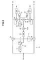
- FIG. 3 is a circuit block diagram of the signal converter circuit 10.
- the input signal Sin is input to vector adder circuits 14, 16, and aphase shifter 12.
- the phase shifter 12 is a circuit for advancing the phase of the input signal Sin by n/2, and its output is input to a variable gain amplifier 18.
- To the variable gain amplifier 18 is input an output signal of a low-pass filter 20 as a gain control signal through a buffer amplifier (not shown), and an amplification gain is controlled according to the gain control signal.
- An output of the variable gain amplifier 18 is supplied to the vector adder circuit 14 as the first constant envelope vector generation signal e, and then added to the input signal Sin by the vector adder circuit 14.
- the first intermediate signal S1 is output from the vector adder circuit 14.
- the first constant envelope vector generation signal e is further supplied to a phase inverter circuit 17, and the first constant envelope vector generation signal e is inverted in phase by the phase inverter circuit 17 to generate the second constant envelope vector generation signal-e.
- the second constant envelope vector generation signal -e is supplied to a vector adder circuit 16, and then added to the input signal Sin by the vector adder circuit 16.
- the second intermediate signal S2 is output from the vector adder circuit 16.
- the output of the vector adder circuit 14 is distributed to a mixer 24 that is a first amplitude detector circuit, and a DC voltage signal indicative of a squared value of the amplitude of the first intermediate signal S1 is generated by the mixer 24.
- the output of the vector adder circuit 16 is distributed to a mixer 26 that is a second amplitude detector circuit, and a DC voltage signal indicative of a squared value of the amplitude of the second intermediate signal S2 is generated by the mixer 26.
- the mixers 24 and 26 may be formed of, for example, a Gilbert cell mixer.
- the outputs of the mixers 24 and 26 are supplied to an adder circuit 28, and a voltage signal indicative of an added value of those outputs is generated by the adder circuit 28.
- the voltage signal is input to an adder circuit 22 to generate a voltage signal indicative of a value obtained by subtracting the output voltage of the adder circuit 28 from a reference voltage Vref.
- the value of the reference voltage Vref corresponds to a sum of squared values of target values (corresponding to the radius of a circle represented in a phase plane of FIG. 2 ) of the amplitudes of the first intermediate signal S1 and the second intermediate signal S2.
- the output signal of the adder circuit 22 passes through the low-pass filter 20 and the buffer amplifier (not shown), and is then supplied to the variable gain amplifier 18 as the gain control signal as described above.
- the amplitude of the first intermediate signal S1 and the amplitude of the second intermediate signal S2 approach a given value based on the reference voltage Vref.
- the output of the mixer 24 is inverted and input to an adder 32, and the output of the mixer 26 is inverted and input to an adder 34.
- the voltage value of the output of the adder circuit 28 is attenuated to 1/2 by an attenuator 30, and the attenuated signal is input to the adders 32 and 34 as a reference amplitude. That is, the adder circuit 28 and the attenuator 30 function as an averaging circuit for generating an average of the amplitudes detected by the mixers 24 and 26, and the average generated by this circuit is set as the reference amplitude.
- the adder 32 outputs a voltage signal indicative of a value obtained by subtracting the output of the mixer 24 from the reference amplitude, and the voltage signal is supplied to a sampling hold circuit 36, and an input voltage at a desired timing is held by the sampling hold circuit 36.
- the voltage signal held by the sampling hold circuit 36 is supplied to the mixer 24, and the detection sensitivity of the mixer 24 used as the first voltage detector circuit is controlled according to this voltage signal.
- the adder 34 outputs a voltage signal indicative of a value obtained by subtracting the output of the mixer 26 from the reference amplitude, and the voltage signal is supplied to a sampling hold circuit 38, and an input voltage at the above-mentioned desired timing is held by the sampling hold circuit 38.
- the voltage signal held by the sampling hold circuit 38 is supplied to the mixer 26, and the detection sensitivity of the mixer 26 used as the voltage detector circuit is controlled according to this signal.
- the reference signal having a given amplitude is input to the signal converter circuit 10 as the input signal Sin by a control circuit (not shown) at a given timing such as an initialization timing of the power amplification device 40.
- the inputs of the first constant envelope vector generation signal e and the second constant envelope vector generation signal -e to the vector adder circuits 14 and 16 are suspended.
- the control circuit instructs the sampling hold circuits 36 and 38 to hold the output voltage signals of the adders 32 and 34.
- the vector adder circuits 14 and 16 both output the reference signal itself, and each of the mixers 24 and 26 outputs a DC voltage signal (calibration signal) corresponding to the amplitude of the same signal.
- a difference between those calibration signals means that there is a difference in the detection sensitivity between the mixers 24 and 26.
- a voltage signal indicative of a difference between the average value (reference amplitude) of the calibration signals and each calibration signal is held by the sampling hold circuits 36 and 38, and the detection sensitivities of the mixers 24 and 26 are controlled by the held signal.
- the mixers 24 and 26 are circuits for outputting a voltage proportional to the amount of supply current from a constant current source, such as a Gilbert cell mixer.
- a constant current source such as a Gilbert cell mixer.
- the amount of supply current is increased or decreased according to the voltage signal held by the sampling hold circuits 36 and 38.
- the reference amplitude is larger than the output of the mixer 24 and smaller than the output of the mixer 26
- the amount of supply current from the constant current source of the mixer 24 is increased, to thereby increase the detection sensitivity of the mixer 24.
- the amount of supply current from the constant current source of the mixer 26 is decreased, to thereby decrease the detection sensitivity of the mixer 26.
- the detection sensitivities of the mixers 24 and 26 are uniformed.
- the detection sensitivities of those mixers 24 and 26 are controlled.
- the detection sensitivity of one of the mixers 24 and 26 maybe so controlled as to uniform the detection sensitivities of those mixers 24 and 26.
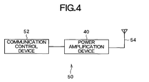
- FIG. 4 is a configuration example of a communication device using the above-mentioned power amplification device 40.
- a signal amplitude-modulated according to transmit information is generated by a communication control device 52, and the generated signal is supplied to a power amplification device 40 as the input signal Sin.
- the power amplification device 40 is connected with a transmit antenna 54, and an amplified output Sout is transmitted wirelessly by the antenna 54.
- the input signal Sin may be appropriately amplified. Further, because the communication device 50 is configured by the power amplification device 40, the communication error may be reduced.
Landscapes
- Engineering & Computer Science (AREA)
- Power Engineering (AREA)
- Amplifiers (AREA)
- Transmitters (AREA)
Abstract
Description
- The present invention relates to a power amplification device and a communication device, and more particularly to a power amplification device for converting an input signal into two constant envelope signals, amplifying those constant envelope signals, and then vectorially adding those amplified signals, and a communication device using the power amplification device.
- In a linear amplification with nonlinear component (LINC) among the power amplification systems used for amplifying a transmit signal in a communication device or the like, after an input signal having an envelope variation has been converted into two constant envelope signals (intermediate signals) having a phase difference corresponding to the amplitude of the input signal, the respective envelope signals are amplified by a nonlinear amplifier. Then, the amplified constant envelope signals are vectorially added to obtain an amplified input signal. According to this system, because the nonlinear amplifier has only to amplify the constant envelope signals, a power amplification efficiency may be improved (for example, refer to Patent Document 1).
- Patent Document 1:
JP 06-22302 B - In a power amplifier circuit disclosed in the
above Patent Document 1, the input signal is converted into two constant envelope signals through digital signal processing. According to this configuration, an analog/digital converter and a digital/analog converter are required, which results in such a problem that the circuit scale is increased. - Under the circumstance, the present applicant has studied a circuit configuration that converts the input signal into two constant envelope signals through analog signal processing. Specifically, as illustrated in
FIG. 5 , in a novelpower amplifier device 100, an input signal Sin is rotated by n/2 through a phase shifter102toobtainanorthogonalsignal, and the signal is amplified by avariable gain amplifier 104 to generate a signal (first constant envelope vector generation signal e). The first constant envelope vector generation signal e is vectorially added to the input signal Sin through anadder circuit 106 to generate a first intermediate signal S1. Further, the first constant envelope vector generation signal e is rotated by n through aphase shifter 110 to generate a phase inversion signal (second constant envelope vector generation signal-e), and the second constant envelope vector generation signal -e is added to the input signal Sin through anadder 108 to generate a second intermediate signal S2. Then, the amplitudes (specifically, the squared amplitudes) of the first and second intermediate signal S1 and S2 are detected by mixers (amplitude detector circuits) 116 and 118, respectively, and a total value of those signals is generated by anadder circuit 120. Further, a difference between the total value and a given voltage Vref is generated by anadder circuit 114. Further, the value is filtered by a low-pass filter 112, and its output is input to thevariable gain amplifier 104 as a gain control signal through a buffer amplifier (not shown). According to this configuration, the gain of thevariable gain amplifier 104 is subjected to feedback control so that the sum of the squared amplitudes of the first and second intermediate signals S1 and S2 becomes a given value indicated by Vref, and the amplitudes of the first and second intermediate signals S1 and S2 are set to desired values. As a result, the respective first and second intermediate signals S1 and S2 maybe set as the constant envelope signals. However, in this configuration, when the detection sensitivities of the amplitudes of the first and second intermediate signals S1 and S2 in themixers - The present invention has been made inviewof the above problem, and an object of the invention is to provide a power amplification device capable of suppressing a variation in an amplitude detection sensitivity of first and second intermediate signals, and a communication device using the power amplification device.
- In order to solve the above-mentioned problem, the present invention provides a power amplification device including: a first intermediate signal generator circuit for adding a first constant envelope vector generation signal orthogonal to an input signal to the input signal to generate a first intermediate signal; a second intermediate signal generation circuit for adding a second constant envelope vector generation signal obtained by inverting the first constant envelope vector generation signal in phase to the input signal to generate a second intermediate signal; a first amplitude detector circuit for detecting an amplitude of the first intermediate signal; a second amplitude detector circuit for detecting an amplitude of the second intermediate signal; an amplitude control circuit for changing the amplitudes of the first constant envelope vector generation signal and the second constant envelope vector generation signal based on the amplitudes detected by the first amplitude detector circuit and the second amplitude detector circuit; a first amplifier circuit for amplifying the first intermediate signal; a second amplifier circuit for amplifying the second intermediate signal; an adder circuit for adding the first amplified intermediate signal and the second amplified intermediate signal together to generate an output signal obtained by amplifying the input signal; a voltage holding circuit for allowing an amplitude of a given reference signal to be detected by at least one of the first amplitude detector circuit and the second amplitude detector circuit to hold a voltage related to the amplitudes; and a correction circuit for correcting a detection sensitivity of the first amplitude detector circuit or the second amplitude detector circuit based on the voltage held by the voltage holding circuit.
- According to the present invention, the amplitude of the given reference signal is detected by the first amplitude detector circuit or the second amplitude detector circuit, and the voltage related to the amplitude detected at this time is held by the voltage holding circuit. The held voltage may be indicative of the detected amplitudes per se, or may be indicative of a difference between the detected amplitudes. Further, the heldvoltage maybe indicative of a difference between the detected amplitude and the given value. In the present invention, because the detection sensitivity of the first amplitude detector circuit and the second amplitude detector circuit is corrected based on the held voltage, a variation in the detection sensitivity may be suppressed.
- Further, in an aspect of the present invention, the voltage holding circuit includes: a first voltage holding circuit for allowing the amplitude of the given reference signal to be detected by the first amplitude detector circuit to hold a voltage indicative of a deviation between the amplitude and a given reference amplitude; and a second voltage holding circuit for allowing the amplitude of the given reference signal to be detected by the second amplitude detector circuit to hold a voltage indicative of a deviation between the amplitude and the given reference amplitude, and the correction circuit includes: a first correction circuit for correcting the detection sensitivity of the first amplitude detector circuit based on the voltage held by the first voltage holding circuit; and a second correction circuit for correcting the detection sensitivity of the second amplitude detector circuit based on the voltage held by the second voltage holding circuit. According to this aspect, the amplitude detection sensitivities of the first amplitude detector circuit and the second amplitude detector circuit may be uniformed.
- In this aspect, when the given reference signal is supplied as the input signal, the first voltage holding circuit may allow the same signal as the given reference signal to be generated as the first intermediate signal by the first intermediate signal generation circuit so that the amplitude of the given reference signal is detected by the first amplitude detector circuit. With this configuration, the amplitude of the given reference amplitude signal maybe easily detected by the first amplitude detector circuit.
- Further, when the given reference signal is supplied as the input signal, the second voltage holding circuit may allow the same signal as the given reference signal to be generated as the second intermediate signal by the second intermediate signal generation circuit so that the amplitude of the given reference signal is detected by the second amplitude detector circuit.
- Further, the power amplification device may further include an averaging circuit for obtaining an average of the amplitude detected from the given reference signal by the first amplitude detector circuit and the amplitude detected from the given reference signal by the second amplitude detector circuit as the given reference amplitude.
- Further, the present invention provides a communication device including any one the above-mentioned power amplification devices, and an antenna and a communication control device which are connected to the power amplification device. According to the present invention, because the transmit signal is amplified by the power amplification device, the communication error may be prevented from increasing.
-
- [
FIG. 1 ] A block diagram illustrating a configuration of a power amplification device according to an embodiment of the present invention. - [
FIG. 2 ] A diagram of an IQ plane illustrating signal processing by a signal converter circuit according to the embodiment of the present invention. - [
FIG. 3 ] A block diagram illustrating a configuration of a signal converter circuit according to the embodiment of the present invention. - [
FIG. 4 ] A block diagram illustrating a configuration of a communication device according to the embodiment of the present invention. - [
FIG. 5 ] A block diagram illustrating a configuration of a signal converter circuit according to the precondition for the present invention. - An embodiment of the present invention is described below in detail with reference to the drawings.
-
FIG. 1 is a configuration diagram of a power amplification device according to an embodiment of the present invention. As illustrated in the figure, apower amplification device 40 includes asignal converter circuit 10,amplifiers vector adder circuit 46. Thesignal converter circuit 10 is an analog signal processor circuit for converting an input signal Sin into a first intermediate signal S1 and a second intermediate signal S2 upon receiving the input signal Sin. As illustrated inFIG. 2 , the first intermediate signal S1 and the second intermediate signal S2 are signals each having a constant envelope. The first intermediate signal S1 has a phase advanced by a given amount relative to the input signal Sin, and the second intermediate signal S2 has a phase delayed by a given amount relative to the input signal Sin. When the first intermediate signal S1 and the second intermediate signal S2 are vectorially synthesized, a signal identical in phase with the original input signal Sin and larger in amplitude by a given number times (twice in this example) than the original input signal Sin is obtained. In this embodiment, a first constant envelope vector generation signal e and a second constant envelope vector generation signal -e are each vectorially added to the input signal Sin to generate the first intermediate signal S1 and the second intermediate signal S2. - Returning to
FIG. 1 , in thepower amplification device 40, the first intermediate signal S1 and the second intermediate signal S2 which are constant envelope signals output from thesignal converter circuit 10 are amplified by theamplifiers amplifiers amplifiers vector adder circuit 46, to thereby obtain an amplified output signal Sout. According to thepower amplification device 40, even if the amplitude of the input signal Sin is changed, theamplifiers amplifiers -
FIG. 3 is a circuit block diagram of thesignal converter circuit 10. As illustrated in the figure, in thesignal converter circuit 10, the input signal Sin is input tovector adder circuits andaphase shifter 12. Thephase shifter 12 is a circuit for advancing the phase of the input signal Sin by n/2, and its output is input to avariable gain amplifier 18. To thevariable gain amplifier 18 is input an output signal of a low-pass filter 20 as a gain control signal through a buffer amplifier (not shown), and an amplification gain is controlled according to the gain control signal. An output of thevariable gain amplifier 18 is supplied to thevector adder circuit 14 as the first constant envelope vector generation signal e, and then added to the input signal Sin by thevector adder circuit 14. As a result, the first intermediate signal S1 is output from thevector adder circuit 14. Further, the first constant envelope vector generation signal e is further supplied to aphase inverter circuit 17, and the first constant envelope vector generation signal e is inverted in phase by thephase inverter circuit 17 to generate the second constant envelope vector generation signal-e. The second constant envelope vector generation signal -e is supplied to avector adder circuit 16, and then added to the input signal Sin by thevector adder circuit 16. As a result, the second intermediate signal S2 is output from thevector adder circuit 16. - The output of the
vector adder circuit 14 is distributed to amixer 24 that is a first amplitude detector circuit, and a DC voltage signal indicative of a squared value of the amplitude of the first intermediate signal S1 is generated by themixer 24. Likewise, the output of thevector adder circuit 16 is distributed to amixer 26 that is a second amplitude detector circuit, and a DC voltage signal indicative of a squared value of the amplitude of the second intermediate signal S2 is generated by themixer 26. Themixers mixers adder circuit 28, and a voltage signal indicative of an added value of those outputs is generated by theadder circuit 28. The voltage signal is input to anadder circuit 22 to generate a voltage signal indicative of a value obtained by subtracting the output voltage of theadder circuit 28 from a reference voltage Vref. The value of the reference voltage Vref corresponds to a sum of squared values of target values (corresponding to the radius of a circle represented in a phase plane ofFIG. 2 ) of the amplitudes of the first intermediate signal S1 and the second intermediate signal S2. The output signal of theadder circuit 22 passes through the low-pass filter 20 and the buffer amplifier (not shown), and is then supplied to thevariable gain amplifier 18 as the gain control signal as described above. - According to this configuration, when the output of the
adder circuit 28 exceeds the reference voltage Vref, the amplification amount of the output of thephase shifter 12 by thevariable gain amplifier 18 is decreased according to the exceeded amount. Further, when the output of theadder circuit 28 falls below the reference voltage Vref, the amplification amount of the output of thephase shifter 12 by thevariable gain amplifier 18 is increased according to the falling amount. With application of this feedback circuit configuration, the amplitude of the first intermediate signal S1 and the amplitude of the second intermediate signal S2 approach a given value based on the reference voltage Vref. - In the
signal converter circuit 10, further, the output of themixer 24 is inverted and input to anadder 32, and the output of themixer 26 is inverted and input to anadder 34. Further, the voltage value of the output of theadder circuit 28 is attenuated to 1/2 by anattenuator 30, and the attenuated signal is input to theadders adder circuit 28 and theattenuator 30 function as an averaging circuit for generating an average of the amplitudes detected by themixers - The
adder 32 outputs a voltage signal indicative of a value obtained by subtracting the output of themixer 24 from the reference amplitude, and the voltage signal is supplied to asampling hold circuit 36, and an input voltage at a desired timing is held by thesampling hold circuit 36. The voltage signal held by thesampling hold circuit 36 is supplied to themixer 24, and the detection sensitivity of themixer 24 used as the first voltage detector circuit is controlled according to this voltage signal. - Similarly, the
adder 34 outputs a voltage signal indicative of a value obtained by subtracting the output of themixer 26 from the reference amplitude, and the voltage signal is supplied to asampling hold circuit 38, and an input voltage at the above-mentioned desired timing is held by thesampling hold circuit 38. The voltage signal held by thesampling hold circuit 38 is supplied to themixer 26, and the detection sensitivity of themixer 26 used as the voltage detector circuit is controlled according to this signal. - In this embodiment, the reference signal having a given amplitude is input to the
signal converter circuit 10 as the input signal Sin by a control circuit (not shown) at a given timing such as an initialization timing of thepower amplification device 40. During this operation, the inputs of the first constant envelope vector generation signal e and the second constant envelope vector generation signal -e to thevector adder circuits sampling hold circuits adders vector adder circuits mixers mixers signal converter circuit 10, a voltage signal indicative of a difference between the average value (reference amplitude) of the calibration signals and each calibration signal is held by thesampling hold circuits mixers - Specifically, the
mixers sampling hold circuits mixer 24 and smaller than the output of themixer 26, the amount of supply current from the constant current source of themixer 24 is increased, to thereby increase the detection sensitivity of themixer 24. Meanwhile, the amount of supply current from the constant current source of themixer 26 is decreased, to thereby decrease the detection sensitivity of themixer 26. On the contrary, when the reference amplitude is smaller than the output of themixer 24 and larger than the output of themixer 26, the amount of supply current from the constant current source of themixer 24 is decreased, to thereby decrease the detection sensitivity of themixer 24. Meanwhile, the amount of supply current from the constant current source of themixer 26 is increased, to thereby increase the detection sensitivity of themixer 26. Thus, the detection sensitivities of themixers mixers mixers mixers -
FIG. 4 is a configuration example of a communication device using the above-mentionedpower amplification device 40. In acommunication device 50 illustrated in the figure, a signal amplitude-modulated according to transmit information is generated by acommunication control device 52, and the generated signal is supplied to apower amplification device 40 as the input signal Sin. Then, thepower amplification device 40 is connected with a transmitantenna 54, and an amplified output Sout is transmitted wirelessly by theantenna 54. - According to the
power amplification device 40 described above, because the detection sensitivities of themixers communication device 50 is configured by thepower amplification device 40, the communication error may be reduced.
Claims (6)
- A power amplification device, comprising:a first intermediate signal generator circuit for adding a first constant envelope vector generation signal orthogonal to an input signal to the input signal to generate a first intermediate signal;a second intermediate signal generation circuit for adding a second constant envelope vector generation signal obtained by inverting the first constant envelope vector generation signal in phase to the input signal to generate a second intermediate signal;a first amplitude detector circuit for detecting an amplitude of the first intermediate signal;a second amplitude detector circuit for detecting an amplitude of the second intermediate signal;an amplitude control circuit for changing the amplitudes of the first constant envelope vector generation signal and the second constant envelope vector generation signal based on the amplitudes detected by the first amplitude detector circuit and the second amplitude detector circuit;a first amplifier circuit for amplifying the first intermediate signal;a second amplifier circuit for amplifying the second intermediate signal;an adder circuit for adding the first amplified intermediate signal and the second amplified intermediate signal together to generate an output signal obtained by amplifying the input signal;a voltage holding circuit for allowing an amplitude of a given reference signal to be detected by at least one of the first amplitude detector circuit and the second amplitude detector circuit to hold a voltage related to the amplitudes; anda correction circuit for correcting a detection sensitivity of the first amplitude detector circuit or the second amplitude detector circuit based on the voltage held by the voltage holding circuit.
- The power amplification device according to claim 1,
wherein the voltage holding circuit comprises:a first voltage holding circuit for allowing the amplitude of the given reference signal to be detected by the first amplitude detector circuit to hold a voltage indicative of a deviation between the amplitude and a given reference amplitude; anda second voltage holding circuit for allowing the amplitude of the given reference signal to be detected by the second amplitude detector circuit to hold a voltage indicative of a deviation between the amplitude and the given reference amplitude, andwherein the correction circuit comprises:a first correction circuit for correcting the detection sensitivity of the first amplitude detector circuit based on the voltage held by the first voltage holding circuit; anda second correction circuit for correcting the detection sensitivity of the second amplitude detector circuit based on the voltage held by the second voltage holding circuit. - The power amplification device according to claim 2, wherein, when the given reference signal is supplied as the input signal, the first voltage holding circuit allows the same signal as the given reference signal to be generated as the first intermediate signal by the first intermediate signal generation circuit so that the amplitude of the given reference signal is detected by the first amplitude detector circuit.
- The power amplification device according to claim 2, wherein, when the given reference signal is supplied as the input signal, the second voltage holding circuit allows the same signal as the given reference signal to be generated as the second intermediate signal by the second intermediate signal generation circuit so that the amplitude of the given reference signal is detected by the second amplitude detector circuit.
- The power amplification device according to claim 2, further comprising an averaging circuit for obtaining an average of the amplitude detected from the given reference signal by the first amplitude detector circuit and the amplitude detected from the given reference signal by the second amplitude detector circuit as the given reference amplitude.
- A communication device, comprising the power amplification device according to claim 1, and an antenna and a communication control device which are connected to the power amplification device.
Applications Claiming Priority (2)
| Application Number | Priority Date | Filing Date | Title |
|---|---|---|---|
| JP2008019924 | 2008-01-30 | ||
| PCT/JP2008/073570 WO2009096132A1 (en) | 2008-01-30 | 2008-12-25 | Power amplification device and communication device |
Publications (2)
| Publication Number | Publication Date |
|---|---|
| EP2246976A1 true EP2246976A1 (en) | 2010-11-03 |
| EP2246976A4 EP2246976A4 (en) | 2013-01-09 |
Family
ID=40912489
Family Applications (1)
| Application Number | Title | Priority Date | Filing Date |
|---|---|---|---|
| EP08871748A Withdrawn EP2246976A4 (en) | 2008-01-30 | 2008-12-25 | POWER AMPLIFICATION DEVICE AND COMMUNICATION DEVICE |
Country Status (6)
| Country | Link |
|---|---|
| US (2) | US8013652B2 (en) |
| EP (1) | EP2246976A4 (en) |
| JP (2) | JP4714790B2 (en) |
| CN (1) | CN101926088B (en) |
| TW (1) | TW200939616A (en) |
| WO (1) | WO2009096132A1 (en) |
Cited By (1)
| Publication number | Priority date | Publication date | Assignee | Title |
|---|---|---|---|---|
| EP3024139A4 (en) * | 2013-06-27 | 2017-03-15 | Fodan Co. Ltd. | Linear compound transmitter in which compound power amplification method is used |
Families Citing this family (7)
| Publication number | Priority date | Publication date | Assignee | Title |
|---|---|---|---|---|
| EP2320561A4 (en) * | 2008-07-29 | 2012-04-11 | Kyocera Corp | POWER AMPLIFICATION DEVICE, AND TRANSMISSION DEVICE AND COMMUNICATION DEVICE USING ALL OF THE SAME |
| JP5086436B2 (en) * | 2008-08-07 | 2012-11-28 | 京セラ株式会社 | Power amplifying device and transmitter and communication device using the same |
| JP2013106128A (en) * | 2011-11-11 | 2013-05-30 | Taiyo Yuden Co Ltd | Front end module |
| JP5772557B2 (en) * | 2011-12-08 | 2015-09-02 | 富士通株式会社 | amplifier |
| JP5451737B2 (en) * | 2011-12-28 | 2014-03-26 | 太陽誘電株式会社 | Front-end module |
| US9413319B2 (en) * | 2014-03-24 | 2016-08-09 | Analog Devices, Inc. | Gain calibration |
| US10171115B1 (en) * | 2017-12-19 | 2019-01-01 | Movandi Corporation | Outphasing calibration in a radio frequency (RF) transmitter device |
Family Cites Families (24)
| Publication number | Priority date | Publication date | Assignee | Title |
|---|---|---|---|---|
| US4279641A (en) * | 1978-08-25 | 1981-07-21 | The Dow Chemical Company | Salt-coated magnesium granules |
| JPS6427323A (en) | 1987-07-22 | 1989-01-30 | Mitsubishi Electric Corp | Transmission equipment |
| JPH0622302B2 (en) | 1988-05-11 | 1994-03-23 | 日本電信電話株式会社 | Amplifier |
| JPH0738717B2 (en) * | 1988-05-26 | 1995-04-26 | 松下電器産業株式会社 | Dropout detection device |
| JPH0793538B2 (en) | 1988-08-19 | 1995-10-09 | 日本電信電話株式会社 | Amplifier |
| JPH0396004A (en) * | 1989-09-07 | 1991-04-22 | Fujitsu Ltd | Power amplifier |
| JPH0399507A (en) * | 1989-09-12 | 1991-04-24 | Fujitsu Ltd | Constant envelope signal synthesizing amplifier |
| JPH0537263A (en) * | 1991-07-30 | 1993-02-12 | Fujitsu Ltd | Constant amplitude wave synthesis amplifier |
| JPH0622302A (en) | 1992-07-01 | 1994-01-28 | Nri & Ncc Co Ltd | Transmission and reproduction method of image information |
| US5402019A (en) * | 1992-08-06 | 1995-03-28 | Tektronix, Inc. | Phase startable clock device |
| DE4420377C2 (en) * | 1993-09-22 | 1998-08-27 | Hewlett Packard Co | Method for generating quadrature signals |
| JPH0974320A (en) * | 1995-09-05 | 1997-03-18 | Nippon Motorola Ltd | Constant-amplitude wave synthesis type power amplifier circuit |
| US6404255B1 (en) * | 1995-09-22 | 2002-06-11 | Thomson Licensing S.A. | Phase shift apparatus |
| US6417712B1 (en) * | 2000-09-27 | 2002-07-09 | Nortel Networks Limited | Phase shifter using sine and cosine weighting functions |
| US6384657B1 (en) * | 2001-03-05 | 2002-05-07 | Tektronix, Inc. | Phase startable clock device having improved stability |
| EP1421687A1 (en) * | 2001-08-16 | 2004-05-26 | Koninklijke Philips Electronics N.V. | Tunable quadrature phase shifter |
| JP2006086857A (en) * | 2004-09-16 | 2006-03-30 | Matsushita Electric Ind Co Ltd | Phase-shifting device |
| JP2006270882A (en) | 2005-03-25 | 2006-10-05 | Japan Radio Co Ltd | High frequency amplifier circuit |
| JP2006339888A (en) * | 2005-05-31 | 2006-12-14 | Japan Radio Co Ltd | High frequency amplifier circuit |
| JP2007104007A (en) * | 2005-09-30 | 2007-04-19 | Toshiba Corp | Quadrature modulator and vector correction method in quadrature modulator |
| JP2008028681A (en) * | 2006-07-20 | 2008-02-07 | Sony Corp | Phase shifter and phase shift method |
| US8457565B2 (en) * | 2007-09-27 | 2013-06-04 | Kyocera Corporation | Power amplifier circuit, and transmitter and wireless communication device using the same |
| EP2214307B1 (en) * | 2007-09-27 | 2013-05-29 | Kyocera Corporation | Power amplifying circuit, and transmitter and wireless communication device using the same |
| JP2009182900A (en) * | 2008-01-31 | 2009-08-13 | Kyocera Corp | Power amplification device and communication device |
-
2008
- 2008-12-25 TW TW097150726A patent/TW200939616A/en unknown
- 2008-12-25 US US12/865,720 patent/US8013652B2/en not_active Expired - Fee Related
- 2008-12-25 EP EP08871748A patent/EP2246976A4/en not_active Withdrawn
- 2008-12-25 CN CN2008801252746A patent/CN101926088B/en not_active Expired - Fee Related
- 2008-12-25 JP JP2009551412A patent/JP4714790B2/en not_active Expired - Fee Related
- 2008-12-25 WO PCT/JP2008/073570 patent/WO2009096132A1/en not_active Ceased
-
2010
- 2010-10-29 JP JP2010244741A patent/JP5106614B2/en not_active Expired - Fee Related
-
2011
- 2011-08-04 US US13/198,650 patent/US8207774B2/en not_active Expired - Fee Related
Non-Patent Citations (3)
| Title |
|---|
| BO SHI ET AL: "A 200MHz IF BiCMOS chip for linear LINC transmitters", SOLID-STATE CIRCUITS CONFERENCE, 1999. ESSCIRC '99. PROCEEDINGS OF THE 25TH EUROPEAN DUISBURG, GERMANY 21-23 SEPT. 1999, PISCATAWAY, NJ, USA,IEEE, 21 September 1999 (1999-09-21), pages 282-285, XP010824249, ISBN: 978-2-86332-246-8 * |
| BO SHI ET AL: "A 200-MHz IF BiCMOS Signal Component Separator for Linear LINC Transmitters", IEEE JOURNAL OF SOLID-STATE CIRCUITS, IEEE SERVICE CENTER, PISCATAWAY, NJ, US, vol. 35, no. 7, 1 July 2000 (2000-07-01), XP011061287, ISSN: 0018-9200 * |
| See also references of WO2009096132A1 * |
Cited By (1)
| Publication number | Priority date | Publication date | Assignee | Title |
|---|---|---|---|---|
| EP3024139A4 (en) * | 2013-06-27 | 2017-03-15 | Fodan Co. Ltd. | Linear compound transmitter in which compound power amplification method is used |
Also Published As
| Publication number | Publication date |
|---|---|
| TW200939616A (en) | 2009-09-16 |
| CN101926088B (en) | 2013-01-02 |
| JP4714790B2 (en) | 2011-06-29 |
| JP2011024270A (en) | 2011-02-03 |
| CN101926088A (en) | 2010-12-22 |
| US20110001541A1 (en) | 2011-01-06 |
| US20110285446A1 (en) | 2011-11-24 |
| JP5106614B2 (en) | 2012-12-26 |
| US8013652B2 (en) | 2011-09-06 |
| US8207774B2 (en) | 2012-06-26 |
| JPWO2009096132A1 (en) | 2011-05-26 |
| EP2246976A4 (en) | 2013-01-09 |
| WO2009096132A1 (en) | 2009-08-06 |
Similar Documents
| Publication | Publication Date | Title |
|---|---|---|
| US8207774B2 (en) | Power amplification device and communication device | |
| US20020181611A1 (en) | Analog quadrature modulator (AQM) error compensating apparatus and method | |
| KR101663970B1 (en) | Time alignment for an amplification stage | |
| EP1667331A1 (en) | Amplifier circuit and amplifying method | |
| US7734263B2 (en) | Transmission circuit and communication device | |
| US8290454B2 (en) | Power amplification device, and transmission device and communication device both using thereof | |
| US8344781B2 (en) | Power amplification device, and transmission device and communication device using same | |
| US20030118126A1 (en) | Apparatus and method for compensating error for analog quadrature modulator (AQM) | |
| EP1949638B1 (en) | Transmission circuit and communication apparatus employing the same | |
| TW201440423A (en) | Auto gain adjusting device and method thereof | |
| US7583940B2 (en) | Transmission circuit and communication apparatus employing the same | |
| CN104124928B (en) | Automatic gain adjustment device and method thereof | |
| EP2211461A1 (en) | Power amplifier circuit, and transmitter and wireless communication device using the same | |
| US7528662B2 (en) | Signal amplification apparatus and signal amplification method | |
| JP2001007869A (en) | Carrier leak suppression circuit | |
| JP5464112B2 (en) | Nonlinear distortion compensation amplifying apparatus and nonlinear distortion compensation method | |
| JP2009182900A (en) | Power amplification device and communication device | |
| JP2001267851A (en) | Distortion compensation amplifier | |
| JP2001119245A (en) | Amplitude modulation device |
Legal Events
| Date | Code | Title | Description |
|---|---|---|---|
| PUAI | Public reference made under article 153(3) epc to a published international application that has entered the european phase |
Free format text: ORIGINAL CODE: 0009012 |
|
| 17P | Request for examination filed |
Effective date: 20100809 |
|
| AK | Designated contracting states |
Kind code of ref document: A1 Designated state(s): AT BE BG CH CY CZ DE DK EE ES FI FR GB GR HR HU IE IS IT LI LT LU LV MC MT NL NO PL PT RO SE SI SK TR |
|
| AX | Request for extension of the european patent |
Extension state: AL BA MK RS |
|
| DAX | Request for extension of the european patent (deleted) | ||
| A4 | Supplementary search report drawn up and despatched |
Effective date: 20121210 |
|
| RIC1 | Information provided on ipc code assigned before grant |
Ipc: H03F 3/24 20060101ALI20121204BHEP Ipc: H03F 1/02 20060101AFI20121204BHEP |
|
| STAA | Information on the status of an ep patent application or granted ep patent |
Free format text: STATUS: THE APPLICATION IS DEEMED TO BE WITHDRAWN |
|
| 18D | Application deemed to be withdrawn |
Effective date: 20130713 |