EP2244351B1 - Non-contact power supply system - Google Patents
Non-contact power supply system Download PDFInfo
- Publication number
- EP2244351B1 EP2244351B1 EP10004254.8A EP10004254A EP2244351B1 EP 2244351 B1 EP2244351 B1 EP 2244351B1 EP 10004254 A EP10004254 A EP 10004254A EP 2244351 B1 EP2244351 B1 EP 2244351B1
- Authority
- EP
- European Patent Office
- Prior art keywords
- power
- signal
- coil
- unit
- power supply
- Prior art date
- Legal status (The legal status is an assumption and is not a legal conclusion. Google has not performed a legal analysis and makes no representation as to the accuracy of the status listed.)
- Active
Links
- 230000005540 biological transmission Effects 0.000 claims description 153
- 238000001514 detection method Methods 0.000 claims description 106
- 230000004044 response Effects 0.000 claims description 89
- 230000010355 oscillation Effects 0.000 claims description 40
- 230000008054 signal transmission Effects 0.000 claims description 30
- 230000009467 reduction Effects 0.000 claims description 6
- 230000005674 electromagnetic induction Effects 0.000 claims description 5
- 238000006243 chemical reaction Methods 0.000 claims description 4
- 239000000758 substrate Substances 0.000 description 24
- 238000010586 diagram Methods 0.000 description 12
- 239000002184 metal Substances 0.000 description 8
- 239000003990 capacitor Substances 0.000 description 7
- 230000004907 flux Effects 0.000 description 5
- 230000008901 benefit Effects 0.000 description 4
- 230000007257 malfunction Effects 0.000 description 4
- 230000007423 decrease Effects 0.000 description 3
- 238000009499 grossing Methods 0.000 description 3
- 239000002699 waste material Substances 0.000 description 3
- 230000007274 generation of a signal involved in cell-cell signaling Effects 0.000 description 2
- 238000000034 method Methods 0.000 description 2
- 230000008569 process Effects 0.000 description 2
- 230000001413 cellular effect Effects 0.000 description 1
- 230000003247 decreasing effect Effects 0.000 description 1
- 230000001419 dependent effect Effects 0.000 description 1
- 230000000694 effects Effects 0.000 description 1
- 238000001914 filtration Methods 0.000 description 1
- 238000010438 heat treatment Methods 0.000 description 1
- 230000006698 induction Effects 0.000 description 1
- 238000003780 insertion Methods 0.000 description 1
- 230000037431 insertion Effects 0.000 description 1
- 239000004065 semiconductor Substances 0.000 description 1
- 230000010356 wave oscillation Effects 0.000 description 1
- 238000004804 winding Methods 0.000 description 1
Images


Classifications
-
- H—ELECTRICITY
- H02—GENERATION; CONVERSION OR DISTRIBUTION OF ELECTRIC POWER
- H02J—CIRCUIT ARRANGEMENTS OR SYSTEMS FOR SUPPLYING OR DISTRIBUTING ELECTRIC POWER; SYSTEMS FOR STORING ELECTRIC ENERGY
- H02J7/00—Circuit arrangements for charging or depolarising batteries or for supplying loads from batteries
- H02J7/0029—Circuit arrangements for charging or depolarising batteries or for supplying loads from batteries with safety or protection devices or circuits
- H02J7/00308—Overvoltage protection
-
- H—ELECTRICITY
- H02—GENERATION; CONVERSION OR DISTRIBUTION OF ELECTRIC POWER
- H02J—CIRCUIT ARRANGEMENTS OR SYSTEMS FOR SUPPLYING OR DISTRIBUTING ELECTRIC POWER; SYSTEMS FOR STORING ELECTRIC ENERGY
- H02J50/00—Circuit arrangements or systems for wireless supply or distribution of electric power
- H02J50/10—Circuit arrangements or systems for wireless supply or distribution of electric power using inductive coupling
- H02J50/12—Circuit arrangements or systems for wireless supply or distribution of electric power using inductive coupling of the resonant type
-
- H—ELECTRICITY
- H02—GENERATION; CONVERSION OR DISTRIBUTION OF ELECTRIC POWER
- H02J—CIRCUIT ARRANGEMENTS OR SYSTEMS FOR SUPPLYING OR DISTRIBUTING ELECTRIC POWER; SYSTEMS FOR STORING ELECTRIC ENERGY
- H02J50/00—Circuit arrangements or systems for wireless supply or distribution of electric power
- H02J50/40—Circuit arrangements or systems for wireless supply or distribution of electric power using two or more transmitting or receiving devices
- H02J50/402—Circuit arrangements or systems for wireless supply or distribution of electric power using two or more transmitting or receiving devices the two or more transmitting or the two or more receiving devices being integrated in the same unit, e.g. power mats with several coils or antennas with several sub-antennas
-
- H—ELECTRICITY
- H02—GENERATION; CONVERSION OR DISTRIBUTION OF ELECTRIC POWER
- H02J—CIRCUIT ARRANGEMENTS OR SYSTEMS FOR SUPPLYING OR DISTRIBUTING ELECTRIC POWER; SYSTEMS FOR STORING ELECTRIC ENERGY
- H02J50/00—Circuit arrangements or systems for wireless supply or distribution of electric power
- H02J50/60—Circuit arrangements or systems for wireless supply or distribution of electric power responsive to the presence of foreign objects, e.g. detection of living beings
-
- H—ELECTRICITY
- H02—GENERATION; CONVERSION OR DISTRIBUTION OF ELECTRIC POWER
- H02J—CIRCUIT ARRANGEMENTS OR SYSTEMS FOR SUPPLYING OR DISTRIBUTING ELECTRIC POWER; SYSTEMS FOR STORING ELECTRIC ENERGY
- H02J50/00—Circuit arrangements or systems for wireless supply or distribution of electric power
- H02J50/80—Circuit arrangements or systems for wireless supply or distribution of electric power involving the exchange of data, concerning supply or distribution of electric power, between transmitting devices and receiving devices
-
- H—ELECTRICITY
- H03—ELECTRONIC CIRCUITRY
- H03H—IMPEDANCE NETWORKS, e.g. RESONANT CIRCUITS; RESONATORS
- H03H7/00—Multiple-port networks comprising only passive electrical elements as network components
- H03H7/38—Impedance-matching networks
-
- H04B5/266—
-
- H04B5/79—
Definitions
- the present invention relates to a non-contact power supply system using electromagnetic induction.
- electric devices e.g., an electric shaver, a power toothbrush and a cellular phone
- secondary batteries as a power source
- various non-contact power supply systems to contactlessly charge the secondary batteries by using electromagnetic induction.
- a primary coil of a power supply device when a primary coil of a power supply device is not magnetically coupled with a secondary coil of an electric device (load device) (a standby mode), an inverter circuit of the power supply device is intermittently driven to suppress power consumption, for example.
- the primary coil is magnetically coupled with the secondary coil (a power supply mode)
- the inverter circuit is continuously driven to supply a large amount of power to the electric device.
- the foreign substrate may be heated by induction heating. Accordingly, coils for signal transmission are provided in both the power supply device and the electric device.
- the inverter circuit of the power supply device is switched from an intermittent operation mode to a continuous operation mode only when a signal is transmitted from the electric device to the power supply device through the coils for signal transmission, thereby preventing the foreign substrate from being heated (see, e.g., Japanese Patent Application Publication Nos. H10-271713 and H8-80042 ).
- the inverter circuit of the power supply device is intermittently driven even in the standby mode in which power is not transmitted to the electric device. Accordingly, a relatively large amount of power is consumed even in the standby mode. Further, since a signal is transmitted from the electric device via the coil thereof for signal transmission, in the conventional case disclosed in Japanese Patent Application Publication No. H10-271713 , an oscillation circuit for oscillating the coil for signal transmission and a second secondary coil which is magnetically coupled with the primary coil of the power supply device and supplied with power from the intermittently driven inverter circuit to supply power to the oscillation circuit are provided in the electric device. Accordingly, there is a problem in that space and cost are required to provide two secondary coils in the electric appliance.
- US 2005/068019 A1 refers to a power supply system comprising a primary side coil, a power transmission apparatus having a primary side circuit for feeding a power voltage resulted from switching a DC voltage which is obtained by rectifying smoothing a commercial power supply to the primary side coil, a secondary side coil magnetically coupled to the primary side coil, and power reception equipment having a secondary side circuit for rectifying and smoothing voltage induced across the secondary side coil, wherein there is provided a power adjusting section for adjusting a level of power to be transmitted according to power required by the power reception equipment.
- the power adjusting section has in the primary side circuit a carrier wave oscillation circuit for supplying a carrier wave to the primary side coil, a demodulation circuit for demodulated signal transmitted from the secondary circuit and receive by the primary side coil, and a power change-over section for selecting a level of power to be transmitted according to an information signal from the power reception equipment and demodulated by the demodulated circuit.
- JP 2002 209344A discloses a non-contact power transmission apparatus arranging in the secondary side of a transformer in which a primary coil and a secondary coil obstructed in a separated loading/unloading manner, a rectifying means, a secondary battery, a load circuit, a signal generating circuit for generating a signal for load detection and an antenna coil for transmission connected to be the output of the signal generator and also arranges in the primary side of the transformer a high frequency inverter an antenna coil for receiving a signal from the transmission antenna and a load detecting circuit for detecting a loading or unloading condition with signal from the reception antenna coil.
- JP H 09147070 discloses a non-contact type information card.
- the electric power energy that is received by a loop antenna or the card is increased. Since the receiving voltage is applied to a variable capacitance element via pure resistance element, the resonance is shifted by the receiving voltage and the receiving efficiency is lowered. Therefore, the voltage received by the antenna of the card is suppressed in the overvoltage is attained.
- JP H 0981708 A discloses an IC card reader-writer provided with discrimination sensor units which discriminate the kind of the IC card at the entrances of card insertion ports.
- the present invention provides a non-contact power supply system capable of reducing power consumption of a power supply device in a standby mode while curtailing the number of coils of a load device to which the power is supplied from the power supply device compared to a conventional case.
- the non-contact power supply system includes a power supply device for transmitting high frequency power; and a load device which contactlessly receives the high frequency power transmitted from the power supply device by electromagnetic induction to supply the high frequency power to a load
- the power supply device includes a power transmission unit having a primary power coil for power transmission and an inverter circuit for supplying high frequency current to the primary power coil; an inquiry unit having a primary signal coil for receiving a signal from the load device and an oscillation circuit, the primary signal coil being connected between output terminals of the oscillation circuit; a signal detection unit for detecting the signal received by the primary signal coil; and a control unit for controlling the power transmission unit according to the signal detected by the signal detection unit
- the load device includes the load; a power reception unit having a secondary power coil for power reception which is magnetically coupled to the primary power coil and a power conversion unit which converts the high frequency power induced in the secondary power coil into power for the load;
- the control unit of the power supply device stops power transmission of the power transmission unit when the signal detection unit detects no signal, and executes power transmission of the power transmission unit when the signal detection unit detects a signal. Accordingly, the power transmission unit of the power supply device can be completely stopped when the power is not supplied from the power supply device to the load device, thereby reducing power consumption of the power supply device in a standby mode. Further, the response unit of the load device is operated by the induced electromotive force generated in the secondary signal coil magnetically coupled to the primary signal coil to transmit a signal from the secondary signal coil.
- the primary power coil and the primary signal coil may be substantially coaxially arranged in the power supply device, and the secondary power coil and the secondary signal coil may be substantially coaxially arranged in the load device.
- the power supply device and the load device can be minimized.
- the electromotive force is induced in the foreign substrate so that the presence of the foreign substrate can be found.
- the primary power coil and the primary signal coil are substantially coaxially arranged, and the secondary power coil and the secondary signal coil are substantially coaxially arranged so that it can be found that the foreign substrate provided between the primary power coil and the secondary power coil is present. Accordingly, it is possible to prevent the foreign substrate from being heated.
- the control unit of the power supply device may drive the inverter circuit intermittently, when it executes the power transmission from the power transmission unit and stop the power transmission from the power transmission unit if the signal detection unit does not detect the signal during a pause period of the inverter circuit.
- the control unit of the power supply device drives the inverter circuit intermittently, when it executes the power transmission from the power transmission unit and stops the power transmission from the power transmission unit if the signal detection unit does not detect the signal during a pause period of the inverter circuit. Consequently, detection accuracy of the signal detection unit is improved so that malfunction of the power transmission unit can be prevented.
- the signal may be an amplitude modulated signal and the signal detection unit of the power supply device may detect an envelope of voltage induced in the primary signal coil and determine that the signal is detected if a detected voltage level exceeds a threshold value.
- control unit of the power supply device when it executes power transmission of the power transmission unit, allows the inverter circuit to be intermittently driven and stops power transmission of the power transmission unit if the signal detection unit detects no signal during a pause period of the inverter circuit.
- the load device may include a load device control unit for transmitting a control command from the response unit to the control unit of the power supply device to instruct stop of the power transmission from the power transmission unit or reduction of transmission power.
- a load device control unit transmits control command from the response unit to instruct stop of power transmission from the power transmission unit of the power supply device, thereby suppressing waste of the power.
- the control unit of the power supply device may not execute the power transmission from the power transmission unit if a signal level detected by the signal detection unit is constant.
- the control unit of the power supply device does not execute power transmission of the power transmission unit if the level of the signal detected by the signal detection unit is smaller than a predetermined determination value.
- the response unit of the load device may have a power circuit which produces operation power from a voltage induced in the secondary signal coil and a modulation circuit which is operated by the operation power produced by the power circuit to output a modulation signal to the secondary signal coil.
- the modulation circuit may produce the signal modulated by varying an impedance of an impedance element connected between the two ends of the secondary signal coil.
- the modulation circuit can be implemented to have a simple configuration.
- the power reception unit of the load device may further have a power circuit for producing operation power of the response unit from the high frequency power induced in the secondary power coil.
- the second power circuit produces the operation power of the response unit by using the high frequency power received by the power reception unit, thus there is an advantage of improving the detection accuracy of the signal detection unit by increasing the power transmitted from the response unit.
- the signal detection unit of the power supply device may further have one or more additional primary signal coils.
- the non-contact power supply system may further include additional one or more load devices, and the load device and the additional load devices may have different types of loads and response units of the load device and the additional load devices may transmit and receive signals of different frequencies according to the types of the loads, and the inquiry unit of the power supply device may allow the oscillation circuit to oscillate at frequencies varying according to the types of the load device and the additional load devices.
- one power supply device can correspond to plural different types of loads.
- the load device may further include an additional power circuit for producing operation power of the response unit from high frequency power induced in the secondary power coil and a load device signal transmission unit operated by the power produced by the additional power circuit to transmit a transmission signal
- the power supply device may include a power supply device signal reception unit for receiving the transmission signal from the load device signal transmission unit.
- the power supply device may further include a modulation circuit for modulating the high frequency power from the power transmission unit by an information signal and the load device may further include a demodulation circuit for demodulating high frequency power induced in the secondary power coil to recover the information signal.
- various information data can be transferred from the power supply device to the load device.
- the oscillation circuit may oscillate intermittently while the signal detection unit does not detect the signal and the oscillation circuit may continuously oscillate if the signal detection unit detects the signal.
- an inner and an outer diameter of the primary signal coil may be substantially identical to those of the secondary signal coil and the inner diameter of the secondary signal coil may be larger than an outer diameter of the secondary power coil.
- the secondary signal coil is arranged outwardly from the secondary power coil 111, thus it is possible to reduce an influence of the secondary power coil when a signal is transmitted from the secondary signal coil.
- the primary signal coil and the secondary signal coil may be arranged between the primary power coil and the secondary power coil while the primary power coil and the secondary power coil are magnetically coupled to each other.
- detection accuracy of the signal detection unit can be improved by reducing a distance between the primary signal coil and the secondary signal coil.
- the oscillation circuit of the inquiry unit may oscillate at a frequency higher than that of the inverter circuit
- the response unit may have a power circuit which produces operation power from a voltage induced in the secondary signal coil and a modulation circuit which is operated by the operation power produced by the power circuit to output a modulation signal of a frequency lower than that of the inverter circuit to the secondary signal coil.
- the signal detection unit detects the signal, it is easy to discriminate the oscillation frequency of the oscillation circuit and the frequency of the inverter circuit. Further, by increasing the oscillation frequency of the oscillation circuit to a relatively highest level, it is possible to suppress waste of power of the oscillation circuit.
- the load device may include a response signal transmission unit which is operated by the high frequency power induced in the secondary power coil to transmit a response signal through the secondary power coil.
- the power supply device may include a response signal reception unit for receiving the response signal through the primary power coil magnetically coupled to the secondary power coil, and when the control unit of the power supply device executes the power transmission from the power transmission unit according to the signal detected by the signal detection unit, the control unit stops the power transmission from the power transmission unit if a period in which the response signal reception unit receives no response signal exceeds a specific period and the control unit continues the power transmission from the power transmission unit if the period in which the response signal reception unit receives no response signal does not exceed the specific period.
- the primary signal is situated in the magnetic field generated around the primary power coil so that a noise component is added to the signal received at the primary signal coil. Accordingly, the detection accuracy of the signal detection unit is reduced, the transmission of the power transmission unit may be stopped, when the load is dislocated, power loss may be increased or the foreign substrate may be heated.
- the power transmission of the power transmission unit is continued while the response signal reception unit receives the response signal transmitted from the response signal transmission unit of the load device and is stopped when the response signal is not received.
- the inverter circuit of the power transmission unit can be continuously driven thus power supply efficiency is improved compared to the case in which the inverter circuit is intermittently driven as described above.
- the load device may include a load device control unit for transmitting a control command from the response unit and the response signal transmission unit to the control unit of the power supply device to instruct stop of the power transmission from the power transmission unit or reduction of transmission power.
- a load device control unit transmits control command from the response unit and the response signal transmission unit to instruct stop of power transmission from the power transmission unit of the power supply device, thereby suppressing waste of the power. Further, since the control command is transmitted from the response signal transmission unit as well as the response unit, reliability of the signal transmission is enhanced and the power transmission unit is securely controlled.
- a non-contact power supply system in accordance with a first embodiment of the present invention includes, as shown in FIG. 1 , a power supply device A which transmits high frequency power and a load device B which receives the high frequency power transmitted from the power supply device A in a non-contact mode by electromagnetic induction to supply the power to a load.
- the power supply device A includes a power transmission unit 1 having a primary power coil 10 for power transmission and an inverter circuit 11 for supplying high frequency current to the primary power coil 10, and an inquiry unit 2 having a primary signal coil 20 for transmitting/receiving a signal to/from the load device B and an oscillation circuit 21, the primary signal coil 20 being connected between output terminals of the oscillation circuit 21.
- the power supply device A further includes a signal detection unit 3 for detecting the signal received by the primary signal coil 20, and a control unit 4 for controlling the power transmission unit 1 according to the signal detected by the signal detection unit 3.
- the inverter circuit 11 converts alternate current (AC) of a low frequency (50 Hz or 60 Hz) supplied from a commercial AC power source (not shown) into current of a high frequency (about 100 kHz) (high frequency current) to supply the high frequency current to the primary power coil 10. Since the inverter circuit 11 is well known in the art, detailed configuration, illustration and description thereof will be omitted.
- the oscillation circuit 21 generates an oscillation signal at a frequency (e.g., 4 MHz) sufficiently higher than the frequency of the inverter circuit 11 to supply the oscillation signal (e.g., sinusoidal signal) to the primary signal coil 20. Since the oscillation circuit 21 is well known in the art, detailed configuration, illustration and description thereof will be omitted.
- the control unit 4 includes a microcomputer as a main component.
- the control unit 4 performs various processes including the control of an operation of the inverter circuit 11 by executing programs stored in a memory (not shown) in the microcomputer.
- the load device B includes a load (e.g., secondary battery) 100, and a power reception unit 110 having a secondary power coil 111 for power reception which is magnetically coupled to the primary power coil 10 and a power conversion unit (rectifier circuit 112 in this embodiment) which converts the high frequency power induced in the secondary power coil 111 into power suitable for the load 100.
- the load device B further includes a secondary signal coil 121 which is magnetically coupled to the primary signal coil 20 and a response unit 120 which is operated by an electromotive force induced in the secondary signal coil 121 to transmit a signal from the secondary signal coil 121.
- the high frequency power induced in the secondary power coil 111 is rectified by the rectifier circuit 112 to charge the secondary battery serving as the load 100.
- the response unit 120 has a power circuit 122 which produces operation power (direct current (DC) voltage) from the induced electromotive force generated in the secondary signal coil 121 and a modulation circuit 123 which is operated by the operation power produced by the power circuit 122 to output a modulation signal to the secondary signal coil 121.
- a resonance capacitor C2 is connected between both ends of the secondary signal coil 121 as shown in Fig. 2 , and the secondary signal coil 121 and the capacitor C2 form a resonance circuit to increase high frequency voltage that is applied to the power circuit 122 or the modulation circuit 123.
- high frequency current flowing in the secondary signal coil 121 is rectified by a diode D1 to charge an electrolytic capacitor C1.
- the electric charges of the electrolytic capacitor C1 are discharged to supply DC voltage to the modulation circuit 123.
- the modulation circuit 123 includes, as shown in FIG. 2 , a series circuit of a rectifying diode D2, a resistor R and a switching element Q1 formed of a bipolar transistor, and a multi-vibrator MV for generating a square wave signal (modulated signal) of a low frequency (about 1 kHz).
- the modulation circuit 123 modulates an amplitude of the high frequency voltage (carrier wave) induced in the secondary signal coil 121 with the square wave signal outputted from the multi-vibrator MV by switching the switching element Q1 with the square wave signal.
- a capacitor or a parallel circuit of capacitors may be provided instead of the resistor R to increase or decrease an impedance (electrostatic capacitance) connected to the secondary signal coil 121 according to on and off of the switching element Q1.
- the signal detection unit 3 demodulates (detects) the modulated signal (square wave signal) by detecting an envelope of the high frequency voltage waveform of the primary signal coil 20.
- each of the set of primary coils 10 and 20 and the set of secondary coils 111 and 121 n is arranged in a plane substantially perpendicular to an axial direction thereof (vertical direction in FIG. 3A ).
- FIG. 4 illustrates a waveform of the high frequency voltage generated in the primary signal coil 20, (b) shows the modulated signal (square wave signal) outputted from the modulation circuit 123, (c) depicts a detection waveform obtained when the signal detection unit 3 detects an envelope of the high frequency voltage waveform of the primary signal coil 20, (d) sets forth a waveform obtained by peak-holding the detection waveform, (e) represents a signal detection result obtained by the signal detection unit 3 (binary signal having a level H when a signal is detected from the load device B and a level L when a signal is not detected from the load device B), (f) illustrates a control signal of the control unit 4 for controlling the power transmission unit 1 (signal for driving the inverter circuit 11 at a level H and stopping the inverter circuit 11 at a level L), and (g) shows a waveform of the high frequency current flowing in the primary power
- the control unit 4 When electric power begins to be supplied to the power supply device A from the commercial AC power source (not shown) (power ON), the control unit 4 outputs a control signal of the level L to stop the inverter circuit 11 of the power transmission unit 1, and the oscillation circuit 21 of the inquiry unit 2 immediately begins to oscillate.
- the amplitude of the waveform of the high frequency voltage generated in the primary signal coil 20 is constant.
- the signal detection unit 3 does not perform envelope detection and outputs a detection result of 'No signal' (signal of the level L) to the control unit 4. Since the signal detection unit 3 detects no signal, the control unit 4 determines that it is in the no-load state and continuously outputs a control signal of the level L such that the inverter circuit 11 of the power transmission unit 1 is maintained in a stopped state.
- an electrically conductive foreign substrate e.g., metal
- the signal detection unit 3 does not perform envelope detection, and outputs a detection result of 'No signal' to the control unit 4. Since the signal detection unit 3 does not detect a signal, the control unit 4 continuously outputs a control signal of the level L, so that the inverter circuit 11 of the power transmission unit 1 is maintained in the stopped state.
- the primary power coil 10 and the primary signal coil 20 are positioned to be magnetically coupled to the secondary power coil 111 and the secondary signal coil 121, respectively.
- the secondary signal coil 121 is magnetically coupled to the primary signal coil 20
- an induced electromotive force is generated in the secondary signal coil 121 and the power circuit 122 produces operation power.
- the modulation circuit 123 begins to be operated by the operation power produced in the power circuit 122 to output a modulation signal to the secondary signal coil 121 (see (b) of FIG. 4 ).
- the carrier wave is amplitude modulated by the modulation circuit 123 (see (a) of FIG. 4 ), and the high frequency voltage waveform of the primary signal coil 20 magnetically coupled to the secondary signal coil 121 is also changed.
- the signal detection unit 3 demodulates (detects) the modulated signal (square wave signal) by detecting an envelope of the high frequency voltage waveform of the primary signal coil 20 (see (c) of FIG. 4 ).
- the signal detection unit 3 performs a peak hold operation on the demodulated square wave signal (see (d) of FIG. 4 ).
- the signal detection unit 3 determines that the load device B is present and outputs a detection result of 'Signal present' (signal of the level H) to the control unit 4 (see (e) of FIG. 4 ).
- the control unit 4 converts a control signal of the level L into a control signal of the level H to drive the inverter circuit 11 of the power transmission unit 1 (see (f) of FIG. 4 ).
- the inverter circuit 11 is driven, high frequency power is transmitted to the power reception unit 110 from the power transmission unit 1 in a non-contact mode to charge the secondary battery serving as the load 100.
- the load device B is transferred from the prescribed position A such that the primary power coil 10 and the primary signal coil 20 cannot be magnetically coupled to the secondary power coil 111 and the secondary signal coil 121, respectively, the aforementioned no-load state is established. Then the signal detection unit 3 outputs the detection result of 'No signal' (signal of the level L) to the control unit 4. The control unit 4 converts the control signal of the level H into the control signal of the level L to stop the inverter circuit 11.
- the control unit 4 of the power supply device A stops power transmission from the power transmission unit 1 when the signal detection unit 3 detects no signal, and executes power transmission from the power transmission unit 1 when the signal detection unit 3 detects a signal. Accordingly, the power transmission unit 1 (inverter circuit 11) of the power supply device A can be completely stopped when the power is not supplied from the power supply device A to the load device B, thereby reducing power consumption of the power supply device A in a standby mode.
- the response unit 120 of the load device B is operated by the induced electromotive force generated in the secondary signal coil 121 magnetically coupled to the primary signal coil 20 to transmit a signal from the secondary signal coil 121. Accordingly, it is unnecessary to provide another coil in addition to the secondary signal coil 121 to supply operation power to the response unit 120 from the power supply device A. As a result, it is possible to reduce power consumption of the power supply device A in the standby mode while reducing the number of coils of the load device B to which the power is supplied from the power supply device A compared to a conventional case.
- a foreign substrate e.g., metal piece
- the control unit 4 may drive the inverter circuit 11 to heat the foreign substrate.
- the control unit 4 it is preferable to detect the foreign substrate (e.g., metal piece) disposed between the primary power coil 10 and the secondary power coil 111 and render the control unit 4 to stop the inverter circuit 11 to prevent the foreign substrate from being heated in such a case.
- the foreign substrate e.g., metal piece
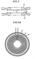
- the primary power coil 10 and the primary signal coil 20 may be preferably coaxially arranged in the power supply device A, and the secondary power coil 111 and the secondary signal coil 121 may be also preferably coaxially arranged in the load device B (see FIG. 5 ).
- the primary power coil 10 and the primary signal coil 20 are formed in a circular shape having the substantially same size, i.e., the same inner and outer diameters, as the secondary power coil 111 and the secondary signal coil 121, respectively.
- the respective coils are arranged in the power supply device A and the load device B such that the primary signal coil 20 and the secondary signal coil 121 are arranged between the primary power coil 10 and the secondary power coil 111 while the primary power coil 10 and the secondary power coil 111 are substantially coaxially arranged to face each other in a magnetically coupled state.
- This arrangement provides an advantage of improving detection accuracy of the signal detection unit 3 by reducing a distance between the primary signal coil 20 and the secondary signal coil 121. Further, it is preferable that the secondary signal coil 121 is influenced as little as possible by another coil (especially, the secondary power coil 111) to allow the carrier wave to be highly modulated. Accordingly, the secondary signal coil 121 is arranged outwardly from the secondary power coil 111 as shown in FIGS. 6A to 8 , thereby reducing an influence of the secondary power coil 111 when a signal is transmitted from the secondary signal coil 121 (when the carrier wave is modulated).
- the secondary coils 111 and 112 are disposed on a same plane and the inner and the outer diameter of the secondary signal coil 121 are greater than the outer diameter of the secondary power coil 111.
- a circular arc-shaped coil wound in a plane is used in this embodiment, it is not limited thereto and a cylindrical, rectangular or elliptical coil may be used.
- FIG. 9 illustrates a waveform of the high frequency voltage generated in the primary signal coil 20, (b) shows a modulated signal (square wave signal) outputted from the modulation circuit 123, (c) depicts a detection waveform obtained when the signal detection unit 3 detects an envelope of the high frequency voltage waveform of the primary signal coil 20, (d) sets forth a waveform obtained by peak-holding the detection waveform, (e) represents a signal detection result obtained by the signal detection unit 3 (binary signal having a level H when a signal is detected from the load device B and a level L when a signal is not detected from the load device B), (f) illustrates a control signal of the control unit 4 for controlling the power transmission unit 1 (signal for driving the inverter circuit 11 at a level H and stopping the inverter circuit 11 at a level L), and (g) shows a waveform of high frequency current flowing in the primary power coil 10.
- the primary power coil 10 and the primary signal coil 20 are positioned to be magnetically coupled to the secondary power coil 111 and the secondary signal coil 121, respectively.
- the secondary signal coil 121 is magnetically coupled to the primary signal coil 20
- an induced electromotive force is generated in the secondary signal coil 121 and the power circuit 122 produces operation power.
- the modulation circuit 123 begins to be operated by the operation power produced in the power circuit 122 to output a modulation signal to the secondary signal coil 121 (see (b) of FIG. 9 ).
- the carrier wave is amplitude modulated by the modulation circuit 123 (see a time period t1 in (a) of FIG. 9 ), and the high frequency voltage waveform of the primary signal coil 20 magnetically coupled to the secondary signal coil 121 is also changed.
- the signal detection unit 3 demodulates (detects) the modulated signal (square wave signal) by detecting an envelope of the high frequency voltage waveform of the primary signal coil 20 (see (c) of FIG. 9 ).
- the signal detection unit 3 performs a peak-hold operation on the demodulated square wave signal (see (d) of FIG. 9 ).
- the signal detection unit 3 determines that the load device B is present and outputs a detection result of 'Signal present' (signal of level H) to the control unit 4 (see (e) of FIG. 9 ).
- the control unit 4 converts a control signal of the level L into a control signal of the level H to drive the inverter circuit 11 of the power transmission unit 1 (see (f) of FIG. 9 ).
- the inverter circuit 11 is driven, high frequency power is transmitted to the power reception unit 110 from the power transmission unit 1 in a non-contact mode to charge the secondary battery serving as the load 100.
- the control unit 4 drives the inverter circuit 11 intermittently. Only the detection result of the signal detection unit 3 obtained during a pause period Tx of the inverter circuit 11 is regarded as valid. If the signal detection unit 3 detects a signal during the pause period Tx, the inverter circuit 11 is intermittently driven, whereas if the signal detection unit 3 detects no signal during the pause period Tx, the inverter circuit 11 is stopped.
- the signal detection unit 3 can accurately detect a signal. Therefore, when the control unit 4 controls the power transmission unit 1 based on the detection result of the signal detection unit 3 obtained during the pause period Tx, malfunction can be prevented during the power transmission of the power transmission unit 1.
- the power circuit 122 does not produce operation power sufficient for the operation of the modulation circuit 123 or the like, a voltage level of the high frequency voltage waveform generated in the primary signal coil 20 decreases (see a time period t2 in (a) of FIG. 9 ).
- the signal detection unit 3 outputs a detection result of 'No signal' (signal of the level L) to the control unit 4 because a peak value of the demodulated square wave signal does not exceeds the threshold value. Consequently, the control unit 4 coverts a control signal of the level H into a control signal of the level L to stop the inverter circuit 11, thereby preventing the metal foreign substrate from being heated by power transmission by the power transmission unit 1.
- FIG. 10 is a flow chart showing a process performed by the control unit 4 of the power supply device A in the above-described operation.
- the frequency (about 1 kHz) of the modulated signal of the modulation circuit 123 is relatively low compared to the oscillation frequency (about 4 MHz) of the oscillation circuit 21 and the frequency (about 100 kHz) of the inverter circuit 11. Accordingly, filtering can be easily performed when the signal detection unit 3 detects an envelope of the modulated signal. Further, both the primary signal coil 20 and the secondary signal coil 121 have a small diameter and a small winding number and are operated with low power consumption by increasing the oscillation frequency of the oscillation circuit 21 to a relatively highest level to increase the AC impedance of the coils 20 and 121and reduce current flowing in the coils 20 and 121.
- the oscillation circuit 21 of the inquiry unit 2 continuously oscillates.
- the oscillation circuit 21 may intermittently oscillate while the signal detection unit 3 detects no signal and may continuously oscillates while the signal detection unit 3 detects a signal. In this case, it is possible to further reduce power consumption in a standby mode compared to the case in which the oscillation circuit 21 continuously oscillates. Further, even in a case where the signal detection unit 3 detects a signal, the oscillation circuit 21 may oscillate only during the pause period Tx the intermittently driven inverter circuit 11 and the oscillation of the oscillation circuit 21 may be stopped during a period in which the inverter circuit 11 is being driven.
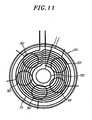
- plural (six in the illustrated example) primary signal coils 20' may be provided in the inquiry unit 2 of the power supply device A.
- the control unit 4 may drive the oscillation circuit 21 of the inquiry unit 2 to oscillate at predetermined multiple frequencies in a time division manner in a standby mode and determines the type of the load device B based on the signal detection results of the signal detection unit 3 at respective oscillation frequencies.
- the load devices B can be identified by the predetermined multiple frequencies set in the oscillation circuit 21 and the resonant frequency determined by the secondary coil 121 and the resonance capacitor C2 of each of the load devices B (see Fig. 2 ).
- the induced electromotive force is hardly generated in the secondary signal coil 121 at a non-resonant frequency so that the modulation circuit can not operate to output a modulation signal to the secondary signal coil 121.
- the induced electromotive force is generated in the secondary signal coil 121 at a resonant frequency and the modulation is performed. Consequently, the power supply device A can identify the load device B coupled thereto for power reception.
- control unit 4 controls the power transmitted from the power transmission unit 1 by increasing or decreasing the frequency of the inverter circuit 11 according to the type of the load device B.
- a non-contact power supply system in accordance with a second embodiment of the present invention has a feature that the load device B further includes a load device control unit 130 for transmitting a control command from the response unit 120 to the control unit 4 of the power supply device A to instruct stop of power transmission of the power transmission unit 1 or reduction of the transmission power level. Since other configurations are same as those of the first embodiment, the same components as those of the first embodiment will be assigned with the same reference numerals and explanation thereof will be omitted.
- the load 100 is a secondary battery and the power is continuously supplied from the power supply device A even after the secondary battery is fully charged, the power is wasted.
- it may be considered to provide a switch element (semiconductor switch element or relay) in a power supply path between the power reception unit 110 and the load 100 such that when the secondary battery is fully charged, the switch element is turned off to interrupt the power supply from the power reception unit 110 to the load 100.
- a switch element semiconductor switch element or relay
- the load device control unit 130 stops the modulation circuit 123 of the response unit 120 such that the signal detection unit 3 of the power supply device A detects no signal.
- the control unit 4 of the power supply device A stops the inverter circuit 11, thereby stopping the power supply of the power transmission unit 1.
- a non-contact power supply system in accordance with a third embodiment of the present invention has a feature that a second power circuit 113 for producing operation power of the response unit 120 from the high frequency power induced in the secondary power coil 111 is provided in the power reception unit 110 of the load device B. Further, since other configurations are same as those of the first embodiment, the same components as those of the first embodiment will be assigned with the same reference numerals and explanation thereof will be omitted.
- the second power circuit 113 supplies DC power to the modulation circuit 123 of the response unit 120, the DC power being produced by rectifying and smoothing the high frequency power induced in the secondary power coil 111 when the power is supplied from the power transmission unit 1 to the power reception unit 110.
- the amount of the power transmitted from the inquiry unit 2 of the power supply device A is very small, and the amount of the operation power produced in the power circuit 122 of the response unit 120 is also very small.
- the second power circuit 113 produces the operation power of the response unit 120 by using the high frequency power received by the power reception unit 110, there is an advantage of improving the detection accuracy of the signal detection unit 3 by increasing the power transmitted from the response unit 120.
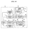
- a non-contact power supply system in accordance with a fourth embodiment of the present invention has a feature that the load device B further includes a second power circuit 113 for producing operation power of the response unit 120 from the high frequency power induced in the secondary power coil 111 and a load device signal transmission unit 124 operated by the power produced in the second power circuit 113 to transmit a transmission signal, and the power supply device A further includes a power supply device side signal reception unit 5 for receiving a signal transmitted from the load device signal transmission unit 124 and a memory 6 for storing information transmitted by the transmission signal.
- the load device signal transmission unit 124 has a transmission coil 124a and transmits, e.g., a frequency-modulated transmission signal through the transmission coil 124a.
- the power supply device side signal reception unit 5 has a reception coil 50 magnetically coupled to the transmission coil 124a and recovers original information by demodulating high frequency voltage (frequency-modulated transmission signal) induced in the reception coil 50.
- the demodulated information is stored in the memory 6. No particular limitation is imposed on the information transmitted from the load device B to the power supply device A by a transmission signal.
- various information data can be transferred between the load device signal transmission unit 124 and the power supply device side signal reception unit 5.
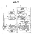
- a non-contact power supply system in accordance with a fifth embodiment of the present invention has a feature that the power supply device A further includes a power supply information signal generation circuit 7 for generating an information signal to be transmitted from the power supply device A to the load device B and a modulation circuit 8 for modulating the high frequency power to be transmitted from the power transmission unit 1 by the information signal, and the load device B further includes a demodulation circuit 140 for demodulating the high frequency power induced in the secondary power coil 111 to recover the information signal, a memory 150 for storing information (information signal) demodulated by the demodulation circuit 140, and a control unit 160 for controlling the load 100 based on the information.
- the same components as those of the first embodiment will be assigned with the same reference numerals and explanation thereof will be omitted.
- the modulation circuit 8 performs modulation (amplitude modulation, frequency modulation, or phase modulation) the high frequency voltage (carrier wave) outputted from the inverter circuit 11 by the information signal (base band signal) generated by the power supply information signal generation circuit 7.
- the demodulation circuit 140 demodulates the high frequency voltage (modulated carrier wave) induced in the secondary power coil 111 to recover the information signal. Further, no particular limitation is imposed on the information transmitted from the power supply device A to the load device B by an information signal.
- various information data can be transferred from the power supply device A to the load device B in this embodiment.
- a non-contact power supply system in accordance with a sixth embodiment of the present invention has a feature that the load device B further includes a response signal transmission unit 170 which is operated by the high frequency power induced in the secondary power coil 111 to transmit a response signal through the secondary power coil 111, and the power supply device A further includes a response signal reception unit 9 for receiving the response signal through the primary power coil 10 magnetically coupled to the secondary power coil 111.
- the response signal transmission unit 170 has a power circuit 171 for producing operation power from the high frequency power induced in the secondary power coil 111 and a modulation circuit 172 which is operated by the operation power produced in the power circuit 171 to perform modulation (e.g., amplitude modulation) on the induced voltage (carrier wave) of the secondary power coil 111. That is, the response signal transmission unit 170 can transmit a response signal only when the power is supplied from the power transmission unit 1 of the power supply device A to the power reception unit 110 of the load device B. The response signal transmission unit 170 cannot transmit a response signal when the power is not supplied from the power transmission unit 1 to the power reception unit 110.
- the response signal transmission unit 170 may continuously or intermittently transmit the response signal.
- the response signal reception unit 9 demodulates the response signal by detecting an envelope of the high frequency voltage waveform of the primary power coil 10 to output the demodulated signal to the control unit 4.
- the signal detection unit 3 is difficult to detect a signal because a large noise component is added to the high frequency voltage waveform generated in the primary signal coil 20. Accordingly, in the first embodiment, the inverter circuit 11 of the power transmission unit 1 is intermittently driven such that the signal detection unit 3 can detect a signal during the pause period of the inverter circuit 11.
- the control unit 4 of the power supply device A continuously executes power transmission of the power transmission unit 1 once the signal detection unit 3 detects a signal representing the presence of the load device B; and the control unit 4 stops the power transmission of the power transmission unit 1 if a period in which the response signal reception unit 9 receives no response signal exceeds a specific period (sufficiently longer than a transmission cycle of the response signal when the response signal is intermittently transmitted) and the control unit 4 continues the power transmission of the power transmission unit 1 if the period in which the response signal reception unit 9 receives no response signal does not exceed the specific period.
- control unit 4 continues or stops the power transmission of the power transmission unit 1 based on whether the response signal reception unit 9 receives the response signal transmitted from the response signal transmission unit 170 of the load device B.
- the inverter circuit 11 of the power transmission unit 1 can be continuously (not intermittently) driven, while preventing malfunction of the power transmission unit 1.
- a non-contact power supply system in accordance with a seventh embodiment of the present invention has a feature that the load device B further includes a load device control unit 130 for transmitting a control command from the response unit 120 and the response signal transmission unit 170 to the control unit 4 of the power supply device A to instruct stop of power transmission of the power transmission unit 1 or reduction of the transmission power level.
- the load device B further includes a load device control unit 130 for transmitting a control command from the response unit 120 and the response signal transmission unit 170 to the control unit 4 of the power supply device A to instruct stop of power transmission of the power transmission unit 1 or reduction of the transmission power level.
- the load device control unit 130 stops the modulation circuit 123 of the response unit 120 such that the signal detection unit 3 of the power supply device A detects no signal.
- the signal detection unit 3 may erroneously detect a noise component as a signal even though the modulation circuit 123 of the response unit 120 is stopped.
- the load device control unit 130 stops both the modulation circuit 123 of the response unit 120 and the modulation circuit 172 of the response signal transmission unit 170 when the secondary battery serving as the load 100 is fully charged. Consequently, the response signal reception unit 9 receives no response signal even when the signal detection unit 3 of the power supply device A detects a wrong signal. Thus, the control unit 4 can stop power transmission of the power transmission unit 1.
Applications Claiming Priority (1)
| Application Number | Priority Date | Filing Date | Title |
|---|---|---|---|
| JP2009104441A JP5554937B2 (ja) | 2009-04-22 | 2009-04-22 | 非接触給電システム |
Publications (3)
| Publication Number | Publication Date |
|---|---|
| EP2244351A2 EP2244351A2 (en) | 2010-10-27 |
| EP2244351A3 EP2244351A3 (en) | 2014-06-04 |
| EP2244351B1 true EP2244351B1 (en) | 2015-09-16 |
Family
ID=42244848
Family Applications (1)
| Application Number | Title | Priority Date | Filing Date |
|---|---|---|---|
| EP10004254.8A Active EP2244351B1 (en) | 2009-04-22 | 2010-04-21 | Non-contact power supply system |
Country Status (9)
| Country | Link |
|---|---|
| US (1) | US8664801B2 (ja) |
| EP (1) | EP2244351B1 (ja) |
| JP (1) | JP5554937B2 (ja) |
| KR (1) | KR101169185B1 (ja) |
| CN (1) | CN101873014B (ja) |
| CA (1) | CA2701255A1 (ja) |
| HK (1) | HK1149126A1 (ja) |
| RU (1) | RU2440635C1 (ja) |
| TW (1) | TWI414121B (ja) |
Cited By (2)
| Publication number | Priority date | Publication date | Assignee | Title |
|---|---|---|---|---|
| US9607757B2 (en) | 2011-11-02 | 2017-03-28 | Panasonic Corporation | Non-contact wireless communication coil, transmission coil, and portable wireless terminal |
| US9667086B2 (en) | 2012-06-28 | 2017-05-30 | Panasonic Intellectual Property Management Co., Ltd. | Mobile terminal |
Families Citing this family (119)
| Publication number | Priority date | Publication date | Assignee | Title |
|---|---|---|---|---|
| EP2083407B1 (de) * | 2008-01-25 | 2012-05-16 | Pepperl + Fuchs GmbH | Vorrichtung und Verfahren zur kontaktlosen Energie- und Datenübertragung |
| DE102009033237A1 (de) | 2009-07-14 | 2011-01-20 | Conductix-Wampfler Ag | Vorrichtung zur induktiven Übertragung elektrischer Energie |
| US8928284B2 (en) * | 2009-09-10 | 2015-01-06 | Qualcomm Incorporated | Variable wireless power transmission |
| US9564939B2 (en) * | 2010-03-12 | 2017-02-07 | Sunrise Micro Devices, Inc. | Power efficient communications |
| IT1400748B1 (it) * | 2010-06-30 | 2013-07-02 | St Microelectronics Srl | Apparato per il trasferimento wireless di energia fra due dispositivi e contemporaneo trasferimento di dati. |
| JP5718619B2 (ja) * | 2010-11-18 | 2015-05-13 | トヨタ自動車株式会社 | コイルユニット、非接触電力送電装置、車両および非接触電力給電システム |
| KR101318848B1 (ko) * | 2010-12-01 | 2013-10-17 | 도요타 지도샤(주) | 비접촉 급전 설비, 차량 및 비접촉 급전 시스템의 제어 방법 |
| CN102611170B (zh) * | 2011-01-21 | 2015-05-13 | 上海泰莱钢结构工程有限公司 | 一种风光互补发电系统对外非接触充电装置 |
| US20130293191A1 (en) | 2011-01-26 | 2013-11-07 | Panasonic Corporation | Non-contact charging module and non-contact charging instrument |
| US10615645B2 (en) | 2011-02-01 | 2020-04-07 | Fu Da Tong Technology Co., Ltd | Power supply device of induction type power supply system and NFC device identification method of the same |
| TWI568125B (zh) * | 2015-01-14 | 2017-01-21 | 富達通科技股份有限公司 | 感應式電源供應器之供電模組及其電壓測量方法 |
| TWI642253B (zh) * | 2017-09-14 | 2018-11-21 | 富達通科技股份有限公司 | 偵測受電模組之方法及供電模組 |
| US10038338B2 (en) | 2011-02-01 | 2018-07-31 | Fu Da Tong Technology Co., Ltd. | Signal modulation method and signal rectification and modulation device |
| US9628147B2 (en) | 2011-02-01 | 2017-04-18 | Fu Da Tong Technology Co., Ltd. | Method of automatically adjusting determination voltage and voltage adjusting device thereof |
| US11128180B2 (en) * | 2011-02-01 | 2021-09-21 | Fu Da Tong Technology Co., Ltd. | Method and supplying-end module for detecting receiving-end module |
| US10630113B2 (en) | 2011-02-01 | 2020-04-21 | Fu Da Tong Technology Co., Ltd | Power supply device of induction type power supply system and RF magnetic card identification method of the same |
| US10056944B2 (en) | 2011-02-01 | 2018-08-21 | Fu Da Tong Technology Co., Ltd. | Data determination method for supplying-end module of induction type power supply system and related supplying-end module |
| TWI570427B (zh) | 2015-10-28 | 2017-02-11 | 富達通科技股份有限公司 | 感應式電源供應器及其金屬異物檢測方法 |
| US9831687B2 (en) | 2011-02-01 | 2017-11-28 | Fu Da Tong Technology Co., Ltd. | Supplying-end module for induction-type power supply system and signal analysis circuit therein |
| US10574095B2 (en) | 2011-02-01 | 2020-02-25 | Fu Da Tong Technology Co., Ltd. | Decoding method for signal processing circuit and signal processing circuit using the same |
| US10289142B2 (en) | 2011-02-01 | 2019-05-14 | Fu Da Tong Technology Co., Ltd. | Induction type power supply system and intruding metal detection method thereof |
| US10312748B2 (en) | 2011-02-01 | 2019-06-04 | Fu Da Tong Techology Co., Ltd. | Signal analysis method and circuit |
| US9600021B2 (en) | 2011-02-01 | 2017-03-21 | Fu Da Tong Technology Co., Ltd. | Operating clock synchronization adjusting method for induction type power supply system |
| US9671444B2 (en) | 2011-02-01 | 2017-06-06 | Fu Da Tong Technology Co., Ltd. | Current signal sensing method for supplying-end module of induction type power supply system |
| US20120223593A1 (en) * | 2011-03-03 | 2012-09-06 | Semiconductor Energy Laboratory Co., Ltd. | Power receiving device and wireless power supply system |
| JP5677875B2 (ja) * | 2011-03-16 | 2015-02-25 | 日立マクセル株式会社 | 非接触電力伝送システム |
| US10003221B2 (en) | 2011-03-31 | 2018-06-19 | Sony Corporation | Detector, power transmitter, power receiver, power feed system, and detection method |
| JP5756925B2 (ja) | 2011-05-19 | 2015-07-29 | パナソニックIpマネジメント株式会社 | 電気機器に設けられた受電装置 |
| JP6067211B2 (ja) * | 2011-05-27 | 2017-01-25 | 日産自動車株式会社 | 非接触給電装置 |
| KR102022350B1 (ko) * | 2011-05-31 | 2019-11-04 | 삼성전자주식회사 | 무선 전력을 이용한 통신 장치 및 방법 |
| CN102347640B (zh) * | 2011-06-09 | 2013-09-18 | 东南大学 | 一种无线能量传输装置 |
| CN106888038A (zh) | 2011-06-14 | 2017-06-23 | 松下电器产业株式会社 | 通信装置 |
| JP5071574B1 (ja) | 2011-07-05 | 2012-11-14 | ソニー株式会社 | 検知装置、受電装置、非接触電力伝送システム及び検知方法 |
| JP5857251B2 (ja) | 2011-08-01 | 2016-02-10 | パナソニックIpマネジメント株式会社 | 非接触給電装置の制御方法及び非接触給電装置 |
| DE102012020565B4 (de) * | 2012-10-19 | 2022-03-03 | Panasonic Intellectual Property Management Co., Ltd. | Kontaktlose Leistungsversorgungsvorrichtung |
| JP5838333B2 (ja) | 2011-08-01 | 2016-01-06 | パナソニックIpマネジメント株式会社 | 非接触給電装置 |
| JP5853199B2 (ja) * | 2011-08-25 | 2016-02-09 | パナソニックIpマネジメント株式会社 | 非接触給電システムの金属異物検出方法、非接触給電装置、電気機器に設けられた受電装置及び非接触給電システム |
| KR20130024757A (ko) * | 2011-08-29 | 2013-03-08 | 주식회사 케이더파워 | 이종 충전 방식을 가진 무선 충전 시스템 |
| JP5794056B2 (ja) | 2011-09-12 | 2015-10-14 | ソニー株式会社 | 給電装置および給電システム |
| FR2980055B1 (fr) * | 2011-09-12 | 2013-12-27 | Valeo Systemes Thermiques | Dispositif de transmission de puissance inductif |
| KR102071833B1 (ko) * | 2011-09-12 | 2020-01-30 | 소니 주식회사 | 송전 장치 및 시스템 |
| JP2013070520A (ja) * | 2011-09-22 | 2013-04-18 | Panasonic Corp | 非接触給電装置の駆動方法、非接触給電装置及び非接触給電システム |
| US9369321B2 (en) * | 2011-09-22 | 2016-06-14 | Northrop Grumman Systems Corporation | Increasing sensor data carrying capability of phase generated carriers |
| KR101273762B1 (ko) * | 2011-09-30 | 2013-06-12 | 삼성전기주식회사 | 무선 충전 시스템 |
| US9722429B2 (en) * | 2011-09-30 | 2017-08-01 | Analogic Corporation | Power delivery to a moving unit |
| CN102355032A (zh) * | 2011-11-01 | 2012-02-15 | 东南大学 | 无线充电装置 |
| US10204734B2 (en) | 2011-11-02 | 2019-02-12 | Panasonic Corporation | Electronic device including non-contact charging module and near field communication antenna |
| US9502920B2 (en) * | 2011-11-16 | 2016-11-22 | Semiconductor Energy Laboratory Co., Ltd. | Power receiving device, power transmission device, and power feeding system |
| JP5168404B1 (ja) * | 2011-12-07 | 2013-03-21 | パナソニック株式会社 | 非接触充電モジュール及びそれを備えた携帯端末 |
| JP2013169122A (ja) | 2012-02-17 | 2013-08-29 | Panasonic Corp | 非接触充電モジュール及びそれを備えた携帯端末 |
| JP5967989B2 (ja) * | 2012-03-14 | 2016-08-10 | ソニー株式会社 | 検知装置、受電装置、送電装置及び非接触給電システム |
| JP2013198322A (ja) | 2012-03-21 | 2013-09-30 | Tokai Rika Co Ltd | 車載非接触充電システム |
| EP2845416B1 (en) * | 2012-05-02 | 2018-11-21 | Apple Inc. | Methods for detecting and identifying a receiver in an inductive power transfer system |
| JP5929493B2 (ja) * | 2012-05-17 | 2016-06-08 | ソニー株式会社 | 受電装置、および、給電システム |
| JP6008237B2 (ja) | 2012-06-28 | 2016-10-19 | パナソニックIpマネジメント株式会社 | 携帯端末 |
| KR101950688B1 (ko) | 2012-07-09 | 2019-02-21 | 삼성전자주식회사 | 무선 전력 송신기 및 그 제어 방법 |
| CN112886715A (zh) * | 2012-07-30 | 2021-06-01 | 皇家飞利浦有限公司 | 无线感应式电力传输 |
| JP6116832B2 (ja) * | 2012-09-03 | 2017-04-19 | 日立マクセル株式会社 | 非接触充電システム |
| US8824597B2 (en) * | 2012-09-07 | 2014-09-02 | Texas Instruments Incorporated | Circuits and methods for field-based communication |
| DE102012019584A1 (de) * | 2012-10-04 | 2014-04-10 | Panasonic Corporation | Verfahren zum Detektieren metallischer Fremdkörper auf kontaktloser Leistungsversorgungsvorrichtung, kontaktlose Leistungsversorgungsvorrichtung, und kontaktlose Leistungsempfangsvorrichtung und kontaktloses Leistungsversorgungssystem |
| US9293251B2 (en) * | 2012-10-11 | 2016-03-22 | Panasonic Intellectual Property Management Co., Ltd. | Method of exciting primary coils in contactless power supplying device and contactless power supplying device |
| KR101372970B1 (ko) * | 2012-10-11 | 2014-03-11 | 파나소닉 주식회사 | 비접촉 급전 장치의 금속 이물질 검출 방법, 비접촉 급전 장치, 수전 장치 및 비접촉 급전 시스템 |
| WO2014063159A2 (en) | 2012-10-19 | 2014-04-24 | Witricity Corporation | Foreign object detection in wireless energy transfer systems |
| KR20150054836A (ko) * | 2012-11-15 | 2015-05-20 | 쥬코쿠 덴료쿠 가부시키 가이샤 | 비접촉 급전 시스템, 및 비접촉 급전 시스템의 제어 방법 |
| CN104798315B (zh) * | 2012-11-29 | 2017-06-20 | 皇家飞利浦有限公司 | 无线感应式电力传输 |
| US9660478B2 (en) * | 2012-12-12 | 2017-05-23 | Qualcomm Incorporated | System and method for facilitating avoidance of wireless charging cross connection |
| AU2013363187B2 (en) * | 2012-12-18 | 2017-07-13 | Nucleus Scientific Inc. | Nonlinear system identification for optimization of wireless power transfer |
| KR102004541B1 (ko) * | 2012-12-31 | 2019-07-26 | 지이 하이브리드 테크놀로지스, 엘엘씨 | 공진형 무선 전력 전송 시스템에서의 무선 전력 전송 제어 방법, 이를 이용하는 무선 전력 전송 장치, 및 이를 이용하는 무선 전력 수신 장치 |
| JP2014212662A (ja) * | 2013-04-19 | 2014-11-13 | キヤノン株式会社 | 送電装置およびその制御方法、電力伝送システム |
| US20140347007A1 (en) * | 2013-05-23 | 2014-11-27 | Broadcom Corporation | Wireless Power Transfer (WPT) for a Mobile Communication Device |
| WO2014195143A1 (en) * | 2013-06-04 | 2014-12-11 | Koninklijke Philips N.V. | Wireless inductive power transfer |
| US10615646B2 (en) * | 2013-07-17 | 2020-04-07 | Koninklijke Philips N.V. | Wireless inductive power transfer |
| WO2015025478A1 (ja) * | 2013-08-21 | 2015-02-26 | パナソニックIpマネジメント株式会社 | 携帯端末充電装置と、それを搭載した自動車 |
| EP3069452A4 (en) * | 2013-11-11 | 2017-07-12 | PowerbyProxi Limited | Power receiver having magnetic signature and method for operating same |
| EP2884622A1 (en) * | 2013-11-20 | 2015-06-17 | Samsung Electro-Mechanics Co., Ltd. | Non-contact power supply device and non-contact power supply method |
| US10170933B2 (en) | 2013-11-20 | 2019-01-01 | Samsung Electro-Mechanics Co., Ltd. | Non-contact type power supplying apparatus and non-contact type power supplying method |
| CN104716748B (zh) * | 2013-12-12 | 2017-05-24 | 深圳大学 | 中距离无线供电系统及其高频变频电源 |
| JP6315382B2 (ja) * | 2013-12-19 | 2018-04-25 | パナソニックIpマネジメント株式会社 | 無線電力伝送のための送電装置および受電装置ならびに無線電力伝送システム |
| GB2525239A (en) | 2014-04-17 | 2015-10-21 | Bombardier Transp Gmbh | Object detection system and method for detecting foreign objects in an inductive power transfer system |
| CN103904786B (zh) * | 2014-04-17 | 2016-07-06 | 长沙海川自动化设备有限公司 | 施工升降机供电装置 |
| DE102014207885A1 (de) * | 2014-04-28 | 2015-10-29 | Continental Automotive Gmbh | Fremdkörpererfassungsvorrichtung und Leistungs-Induktivladevorrichtung |
| GB2526307A (en) * | 2014-05-20 | 2015-11-25 | Bombardier Transp Gmbh | A housing for at least one object detection device, a primary unit and a pavement slab assembly |
| KR102491037B1 (ko) | 2014-05-26 | 2023-01-19 | 지이 하이브리드 테크놀로지스, 엘엘씨 | 무선전력 수신 장치 및 무선 통신 방법 |
| KR20230129621A (ko) | 2014-05-26 | 2023-09-08 | 지이 하이브리드 테크놀로지스, 엘엘씨 | 무접점 전력 수신 장치 및 수신 방법 |
| KR101530491B1 (ko) * | 2014-08-18 | 2015-06-22 | 숭실대학교산학협력단 | 칩 간 무선 전송을 위한 무선 칩 |
| BR112017004943B1 (pt) * | 2014-09-16 | 2022-07-19 | Koninklijke Philips N.V. | Transmissor de energia para fornecer de modo sem fio energia para um receptor de energia por meio de um sinal indutivo de potência, método para operar um transmissor de energia, e sistema de transferência de potência sem fio |
| CN104282238A (zh) * | 2014-10-29 | 2015-01-14 | 安徽省科普产品工程研究中心有限责任公司 | 一种三维立体led广告牌 |
| CN104390662A (zh) * | 2014-11-21 | 2015-03-04 | 国家电网公司 | 基于感应取能技术的变电设备综合状态监测系统 |
| US10153665B2 (en) | 2015-01-14 | 2018-12-11 | Fu Da Tong Technology Co., Ltd. | Method for adjusting output power for induction type power supply system and related supplying-end module |
| CN107408839B (zh) * | 2015-04-06 | 2020-08-28 | 松下知识产权经营株式会社 | 非接触供电装置及其控制装置 |
| US20160301238A1 (en) * | 2015-04-10 | 2016-10-13 | Intel Corporation | Managing presence and long beacon extension pulses |
| US9602955B2 (en) | 2015-05-20 | 2017-03-21 | Empire Technology Development Llc | Concurrent wireless power transfer and data communication |
| EP3304691A4 (en) | 2015-06-03 | 2019-01-23 | Apple Inc. | INDUCTIVE POWER RECEIVER |
| JP6350399B2 (ja) * | 2015-06-10 | 2018-07-04 | トヨタ自動車株式会社 | 非接触送電装置及び電力伝送システム |
| KR20170014879A (ko) * | 2015-07-31 | 2017-02-08 | 삼성전기주식회사 | 무선 전력 송신 장치 및 방법 |
| JP6342369B2 (ja) * | 2015-08-21 | 2018-06-13 | 矢崎総業株式会社 | 電力伝送通信ユニット |
| DE102016215273A1 (de) * | 2015-08-21 | 2017-02-23 | Yazaki Corporation | Leistungsübertragungs-kommunikationseinheit |
| JP6555010B2 (ja) * | 2015-08-25 | 2019-08-07 | 船井電機株式会社 | 給電装置 |
| JP2017103858A (ja) * | 2015-11-30 | 2017-06-08 | オムロン株式会社 | 非接触給電システム |
| US11303156B2 (en) | 2015-12-18 | 2022-04-12 | General Electric Company | Contactless power transfer system and method for controlling the same |
| US10530196B2 (en) * | 2016-02-05 | 2020-01-07 | Texas Instruments Incorporated | Methods and apparatus for power loss calibration in a wireless power system |
| CN106560970B (zh) * | 2016-03-21 | 2023-09-01 | 中兴新能源汽车有限责任公司 | 无线充电接收装置、电动汽车和无线充电系统 |
| EP3493364B1 (en) * | 2016-07-29 | 2020-11-04 | Sony Semiconductor Solutions Corporation | Power-supplying system |
| DE102016120254A1 (de) * | 2016-10-24 | 2018-04-26 | Endress+Hauser Conducta Gmbh+Co. Kg | Schaltung zur Energieversorgung eines Verbrauchers und zum Empfang von vom Verbraucher gesendeten Nutzsignalen |
| JP6754669B2 (ja) * | 2016-10-31 | 2020-09-16 | 株式会社ダイヘン | 給電側装置および給電システム |
| EP3327897B1 (en) * | 2016-11-25 | 2021-06-16 | Nxp B.V. | Apparatus and associated method |
| JP6945188B2 (ja) * | 2016-11-30 | 2021-10-06 | パナソニックIpマネジメント株式会社 | 無線給電ユニット、送電モジュール、受電モジュールおよび無線電力伝送システム |
| US11223240B2 (en) * | 2016-12-15 | 2022-01-11 | General Electric Company | Charging pad and a method for charging one or more receiver devices |
| JP6834698B2 (ja) * | 2017-03-31 | 2021-02-24 | Tdk株式会社 | 磁気結合装置およびこれを用いたワイヤレス電力伝送システム |
| CN117748763A (zh) * | 2017-06-06 | 2024-03-22 | 通用电气公司 | 无线充电装置和接收器装置 |
| EP3429060A1 (en) * | 2017-07-13 | 2019-01-16 | Koninklijke Philips N.V. | Wireless power transfer |
| JP7118532B2 (ja) * | 2018-04-27 | 2022-08-16 | 矢崎総業株式会社 | コネクタ、及び、電力供給システム |
| JP7109983B2 (ja) * | 2018-04-27 | 2022-08-01 | 矢崎総業株式会社 | 車両情報表示システム |
| CN109698558B (zh) * | 2018-12-03 | 2024-03-29 | 深圳市启天太一科技有限公司 | 一种具有降噪设计的无线能量传输装置 |
| CN112421787B (zh) * | 2019-08-21 | 2023-12-19 | 北京小米移动软件有限公司 | 无线充电装置、系统、控制方法、充电设备及存储介质 |
| KR102274007B1 (ko) * | 2019-11-18 | 2021-07-08 | (주)원컴 | 무선 충전 장치에 적용되는 위치 검출 유닛 |
| DE102020133178A1 (de) * | 2019-12-16 | 2021-06-17 | Avago Technologies International Sales Pte. Limited | Kommunikationssystem in drahtloser Leistungsübertragung |
| CN113726028B (zh) * | 2020-06-05 | 2023-02-03 | 华为技术有限公司 | 一种电子设备及其控制方法 |
| JP2023063769A (ja) * | 2021-10-25 | 2023-05-10 | キヤノン株式会社 | 制御システムおよび制御システムの制御方法 |
Family Cites Families (42)
| Publication number | Priority date | Publication date | Assignee | Title |
|---|---|---|---|---|
| SU1464235A1 (ru) | 1987-04-06 | 1989-03-07 | Предприятие П/Я А-1586 | Устройство дл бесконтактной передачи электроэнергии от неподвижного объекта к подвижному |
| JPH0696300A (ja) * | 1992-09-14 | 1994-04-08 | Masuo Ikeuchi | 電磁誘導結合による非接触型icカードおよびリーダライタ |
| GB9310545D0 (en) | 1993-05-21 | 1993-07-07 | Era Patents Ltd | Power coupling |
| US5706183A (en) * | 1994-06-27 | 1998-01-06 | Matsushita Electric Works, Ltd. | Inverter power supply with single discharge path |
| JP3416863B2 (ja) | 1994-06-27 | 2003-06-16 | 松下電工株式会社 | 電源装置 |
| JPH0981708A (ja) * | 1995-09-14 | 1997-03-28 | Tokico Ltd | Icカード及びicカード読み取り装置及びicカード書き込み装置 |
| US7176589B2 (en) * | 1995-09-22 | 2007-02-13 | Input/Output, Inc. | Electrical power distribution and communication system for an underwater cable |
| JP3761001B2 (ja) * | 1995-11-20 | 2006-03-29 | ソニー株式会社 | 非接触型情報カード及びic |
| CA2276338C (en) | 1997-01-03 | 2008-07-29 | Schleifring Und Apparatebau Gmbh | Device for contactless transmission of electrical signals and/or energy |
| DE19701357C2 (de) * | 1997-01-16 | 2003-02-27 | Schleifring Und Appbau Gmbh | Vorrichtung zur kontaktlosen Energieübertragung zwischen gegeneinander beweglichen Teilen |
| JPH10215530A (ja) * | 1997-01-28 | 1998-08-11 | Matsushita Electric Works Ltd | 非接触電力伝送装置 |
| JP3363341B2 (ja) * | 1997-03-26 | 2003-01-08 | 松下電工株式会社 | 非接触電力伝達装置 |
| WO1998058347A1 (fr) * | 1997-06-18 | 1998-12-23 | Mitsubishi Denki Kabushiki Kaisha | Syteme de cartes a circuit integre sans contact et carte a circuit integre sans contact |
| JPH1119229A (ja) * | 1997-07-09 | 1999-01-26 | Nec Corp | 無線による電力と制御信号の伝送方法 |
| JPH11126240A (ja) * | 1997-10-24 | 1999-05-11 | Kokusai Electric Co Ltd | リーダライタコントローラとその送信制御方法 |
| NZ329195A (en) | 1997-11-17 | 2000-07-28 | Auckland Uniservices Ltd | Loosely coupled inductive power transfer using resonant pickup circuit, inductor core chosen to saturate under overload conditions |
| JP3247328B2 (ja) * | 1997-12-09 | 2002-01-15 | 浩 坂本 | 非接触電力伝達装置 |
| JP3465075B2 (ja) * | 1998-12-02 | 2003-11-10 | 株式会社椿本チエイン | 非接触給電装置 |
| JP3743193B2 (ja) * | 1999-02-23 | 2006-02-08 | 松下電工株式会社 | 非接触電力伝達装置 |
| ATE279047T1 (de) * | 2000-04-18 | 2004-10-15 | Schleifring Und Appbau Gmbh | Anordnung zur kontaktlosen übertragung elektrischer signale bzw. energie |
| FI20002493A (fi) * | 2000-11-14 | 2002-05-15 | Salcomp Oy | Teholähdejärjestely ja induktiivisesti kytketty akkulaturi, jossa on langattomasti kytketty ohjaus, ja menetelmä teholähdejärjestelyn ja induktiivisesti kytketyn akkulaturin ohjaamiseksi langattomasti |
| JP2002209344A (ja) * | 2001-01-12 | 2002-07-26 | Matsushita Electric Works Ltd | 非接触電力伝送装置 |
| US7116722B2 (en) * | 2001-02-09 | 2006-10-03 | Lucent Technologies Inc. | Wireless communication system using multi-element antenna having a space-time architecture |
| JP2002252937A (ja) * | 2001-02-26 | 2002-09-06 | Yazaki Corp | 給電装置 |
| JP2003037950A (ja) | 2001-07-26 | 2003-02-07 | Matsushita Electric Works Ltd | 非接触電力伝達装置 |
| JP2004229406A (ja) | 2003-01-23 | 2004-08-12 | Sony Corp | 分離トランス装置 |
| KR100488524B1 (ko) * | 2003-04-09 | 2005-05-11 | 삼성전자주식회사 | 로봇충전장치 |
| JP2005110409A (ja) * | 2003-09-30 | 2005-04-21 | Sharp Corp | 電力供給システム |
| US7233137B2 (en) * | 2003-09-30 | 2007-06-19 | Sharp Kabushiki Kaisha | Power supply system |
| KR100564256B1 (ko) | 2004-06-25 | 2006-03-29 | 주식회사 한림포스텍 | 무선주파수 식별기술이 적용된 무선 충전용 패드 및배터리팩 |
| JP4408250B2 (ja) | 2004-09-07 | 2010-02-03 | 株式会社リコー | 充電システム |
| JP5024740B2 (ja) * | 2004-09-30 | 2012-09-12 | 学校法人慶應義塾 | Lsiチップ試験装置 |
| CN100403241C (zh) * | 2004-12-09 | 2008-07-16 | 张定港 | 非接触式电源感应电路及其应用 |
| JP2006230129A (ja) * | 2005-02-18 | 2006-08-31 | Nanao Corp | 非接触電力供給装置 |
| CN2850099Y (zh) * | 2005-09-26 | 2006-12-20 | 珠海市共创有限公司 | 一种高转换效率非接触式充电装置 |
| CN100367624C (zh) * | 2005-11-07 | 2008-02-06 | 珠海市共创有限公司 | 一种高转换效率非接触式充电装置 |
| JP4775176B2 (ja) | 2006-08-25 | 2011-09-21 | パナソニック電工株式会社 | 電源回路及び電源システム |
| JP2008109762A (ja) * | 2006-10-24 | 2008-05-08 | Olympus Imaging Corp | 電力伝送装置 |
| FR2914512A1 (fr) | 2007-03-27 | 2008-10-03 | Delachaux Sa Sa | Systeme d'alimentation electrique et de transmission de donnees sans contact electrique. |
| KR100819753B1 (ko) | 2007-07-13 | 2008-04-08 | 주식회사 한림포스텍 | 배터리팩 솔루션을 위한 무접점충전시스템 및 그 제어방법 |
| JP2009027781A (ja) * | 2007-07-17 | 2009-02-05 | Seiko Epson Corp | 受電制御装置、受電装置、無接点電力伝送システム、充電制御装置、バッテリ装置および電子機器 |
| US7960867B2 (en) * | 2007-11-27 | 2011-06-14 | Extremely Ingenious Engineering | Methods and systems for wireless energy and data transmission |
-
2009
- 2009-04-22 JP JP2009104441A patent/JP5554937B2/ja active Active
-
2010
- 2010-04-21 CN CN2010101701392A patent/CN101873014B/zh active Active
- 2010-04-21 RU RU2010115891/07A patent/RU2440635C1/ru not_active IP Right Cessation
- 2010-04-21 EP EP10004254.8A patent/EP2244351B1/en active Active
- 2010-04-21 CA CA2701255A patent/CA2701255A1/en not_active Abandoned
- 2010-04-22 US US12/662,548 patent/US8664801B2/en active Active
- 2010-04-22 TW TW099112679A patent/TWI414121B/zh active
- 2010-04-22 KR KR1020100037441A patent/KR101169185B1/ko active IP Right Grant
-
2011
- 2011-03-30 HK HK11103261.3A patent/HK1149126A1/xx unknown
Cited By (4)
| Publication number | Priority date | Publication date | Assignee | Title |
|---|---|---|---|---|
| US9607757B2 (en) | 2011-11-02 | 2017-03-28 | Panasonic Corporation | Non-contact wireless communication coil, transmission coil, and portable wireless terminal |
| US9634515B2 (en) | 2011-11-02 | 2017-04-25 | Panasonic Corporation | Non-contact wireless communication coil, transmission coil, and portable wireless terminal |
| US9667086B2 (en) | 2012-06-28 | 2017-05-30 | Panasonic Intellectual Property Management Co., Ltd. | Mobile terminal |
| US11616395B2 (en) | 2012-06-28 | 2023-03-28 | Sovereign Peak Ventures, Llc | Mobile terminal and chargeable communication module |
Also Published As
| Publication number | Publication date |
|---|---|
| US20100270867A1 (en) | 2010-10-28 |
| KR101169185B1 (ko) | 2012-07-30 |
| TWI414121B (zh) | 2013-11-01 |
| US8664801B2 (en) | 2014-03-04 |
| JP5554937B2 (ja) | 2014-07-23 |
| TW201044740A (en) | 2010-12-16 |
| EP2244351A2 (en) | 2010-10-27 |
| EP2244351A3 (en) | 2014-06-04 |
| CN101873014A (zh) | 2010-10-27 |
| CA2701255A1 (en) | 2010-10-22 |
| KR20100116556A (ko) | 2010-11-01 |
| RU2010115891A (ru) | 2011-10-27 |
| HK1149126A1 (en) | 2011-09-23 |
| CN101873014B (zh) | 2013-03-27 |
| RU2440635C1 (ru) | 2012-01-20 |
| JP2010259172A (ja) | 2010-11-11 |
Similar Documents
| Publication | Publication Date | Title |
|---|---|---|
| EP2244351B1 (en) | Non-contact power supply system | |
| US10892648B2 (en) | Wireless power transfer method, apparatus and system for low and medium power | |
| US9229069B2 (en) | Method for detecting metal foreign object on contactless power supply device, contactless power supply device, contactless power reception device, and contactless power supply system | |
| CN107148719B (zh) | 用于功率传输的系统和方法 | |
| US8129942B2 (en) | Contactless charging method for charging battery | |
| JP5838333B2 (ja) | 非接触給電装置 | |
| CN106981930B (zh) | 送电装置及无线电力传送系统 | |
| JP5857251B2 (ja) | 非接触給電装置の制御方法及び非接触給電装置 | |
| US11175428B2 (en) | Metallic foreign object detector, wireless power transmitting device, wireless power receiving device, and wireless power transmission system | |
| JP6279452B2 (ja) | 非接触電力伝送装置 | |
| JP2022515589A (ja) | 無線電力伝送のための装置および方法 | |
| KR101383731B1 (ko) | 비접촉 급전 장치 | |
| WO2015104768A1 (ja) | 非接触給電装置の制御方法及び非接触給電装置 |
Legal Events
| Date | Code | Title | Description |
|---|---|---|---|
| PUAI | Public reference made under article 153(3) epc to a published international application that has entered the european phase |
Free format text: ORIGINAL CODE: 0009012 |
|
| AK | Designated contracting states |
Kind code of ref document: A2 Designated state(s): AT BE BG CH CY CZ DE DK EE ES FI FR GB GR HR HU IE IS IT LI LT LU LV MC MK MT NL NO PL PT RO SE SI SK SM TR |
|
| AX | Request for extension of the european patent |
Extension state: AL BA ME RS |
|
| RAP1 | Party data changed (applicant data changed or rights of an application transferred) |
Owner name: PANASONIC CORPORATION |
|
| PUAL | Search report despatched |
Free format text: ORIGINAL CODE: 0009013 |
|
| 17P | Request for examination filed |
Effective date: 20140331 |
|
| RBV | Designated contracting states (corrected) |
Designated state(s): AT BE BG CH CY CZ DE DK EE ES FI FR GB GR HR HU IE IS IT LI LT LU LV MC MK MT NL NO PL PT RO SE SI SK SM TR |
|
| AK | Designated contracting states |
Kind code of ref document: A3 Designated state(s): AT BE BG CH CY CZ DE DK EE ES FI FR GB GR HR HU IE IS IT LI LT LU LV MC MK MT NL NO PL PT RO SE SI SK SM TR |
|
| AX | Request for extension of the european patent |
Extension state: AL BA ME RS |
|
| RIC1 | Information provided on ipc code assigned before grant |
Ipc: H02J 7/02 20060101AFI20140429BHEP |
|
| REG | Reference to a national code |
Ref country code: DE Ref legal event code: R079 Ref document number: 602010027503 Country of ref document: DE Free format text: PREVIOUS MAIN CLASS: H02J0007020000 Ipc: H02J0005000000 |
|
| RIC1 | Information provided on ipc code assigned before grant |
Ipc: H02J 5/00 20060101AFI20141219BHEP Ipc: H02J 7/02 20060101ALI20141219BHEP |
|
| GRAP | Despatch of communication of intention to grant a patent |
Free format text: ORIGINAL CODE: EPIDOSNIGR1 |
|
| INTG | Intention to grant announced |
Effective date: 20150210 |
|
| RAP1 | Party data changed (applicant data changed or rights of an application transferred) |
Owner name: PANASONIC INTELLECTUAL PROPERTY MANAGEMENT CO., LT |
|
| GRAP | Despatch of communication of intention to grant a patent |
Free format text: ORIGINAL CODE: EPIDOSNIGR1 |
|
| GRAJ | Information related to disapproval of communication of intention to grant by the applicant or resumption of examination proceedings by the epo deleted |
Free format text: ORIGINAL CODE: EPIDOSDIGR1 |
|
| GRAP | Despatch of communication of intention to grant a patent |
Free format text: ORIGINAL CODE: EPIDOSNIGR1 |
|
| INTG | Intention to grant announced |
Effective date: 20150428 |
|
| INTG | Intention to grant announced |
Effective date: 20150511 |
|
| GRAS | Grant fee paid |
Free format text: ORIGINAL CODE: EPIDOSNIGR3 |
|
| GRAA | (expected) grant |
Free format text: ORIGINAL CODE: 0009210 |
|
| AK | Designated contracting states |
Kind code of ref document: B1 Designated state(s): AT BE BG CH CY CZ DE DK EE ES FI FR GB GR HR HU IE IS IT LI LT LU LV MC MK MT NL NO PL PT RO SE SI SK SM TR |
|
| REG | Reference to a national code |
Ref country code: GB Ref legal event code: FG4D |
|
| REG | Reference to a national code |
Ref country code: CH Ref legal event code: EP |
|
| REG | Reference to a national code |
Ref country code: IE Ref legal event code: FG4D |
|
| REG | Reference to a national code |
Ref country code: AT Ref legal event code: REF Ref document number: 750485 Country of ref document: AT Kind code of ref document: T Effective date: 20151015 |
|
| REG | Reference to a national code |
Ref country code: DE Ref legal event code: R096 Ref document number: 602010027503 Country of ref document: DE |
|
| REG | Reference to a national code |
Ref country code: NL Ref legal event code: MP Effective date: 20150916 |
|
| PG25 | Lapsed in a contracting state [announced via postgrant information from national office to epo] |
Ref country code: LT Free format text: LAPSE BECAUSE OF FAILURE TO SUBMIT A TRANSLATION OF THE DESCRIPTION OR TO PAY THE FEE WITHIN THE PRESCRIBED TIME-LIMIT Effective date: 20150916 Ref country code: FI Free format text: LAPSE BECAUSE OF FAILURE TO SUBMIT A TRANSLATION OF THE DESCRIPTION OR TO PAY THE FEE WITHIN THE PRESCRIBED TIME-LIMIT Effective date: 20150916 Ref country code: NO Free format text: LAPSE BECAUSE OF FAILURE TO SUBMIT A TRANSLATION OF THE DESCRIPTION OR TO PAY THE FEE WITHIN THE PRESCRIBED TIME-LIMIT Effective date: 20151216 Ref country code: GR Free format text: LAPSE BECAUSE OF FAILURE TO SUBMIT A TRANSLATION OF THE DESCRIPTION OR TO PAY THE FEE WITHIN THE PRESCRIBED TIME-LIMIT Effective date: 20151217 Ref country code: LV Free format text: LAPSE BECAUSE OF FAILURE TO SUBMIT A TRANSLATION OF THE DESCRIPTION OR TO PAY THE FEE WITHIN THE PRESCRIBED TIME-LIMIT Effective date: 20150916 |
|
| REG | Reference to a national code |
Ref country code: LT Ref legal event code: MG4D |
|
| REG | Reference to a national code |
Ref country code: AT Ref legal event code: MK05 Ref document number: 750485 Country of ref document: AT Kind code of ref document: T Effective date: 20150916 |
|
| PG25 | Lapsed in a contracting state [announced via postgrant information from national office to epo] |
Ref country code: SE Free format text: LAPSE BECAUSE OF FAILURE TO SUBMIT A TRANSLATION OF THE DESCRIPTION OR TO PAY THE FEE WITHIN THE PRESCRIBED TIME-LIMIT Effective date: 20150916 Ref country code: HR Free format text: LAPSE BECAUSE OF FAILURE TO SUBMIT A TRANSLATION OF THE DESCRIPTION OR TO PAY THE FEE WITHIN THE PRESCRIBED TIME-LIMIT Effective date: 20150916 |
|
| PG25 | Lapsed in a contracting state [announced via postgrant information from national office to epo] |
Ref country code: NL Free format text: LAPSE BECAUSE OF FAILURE TO SUBMIT A TRANSLATION OF THE DESCRIPTION OR TO PAY THE FEE WITHIN THE PRESCRIBED TIME-LIMIT Effective date: 20150916 |
|
| PG25 | Lapsed in a contracting state [announced via postgrant information from national office to epo] |
Ref country code: ES Free format text: LAPSE BECAUSE OF FAILURE TO SUBMIT A TRANSLATION OF THE DESCRIPTION OR TO PAY THE FEE WITHIN THE PRESCRIBED TIME-LIMIT Effective date: 20150916 Ref country code: IT Free format text: LAPSE BECAUSE OF FAILURE TO SUBMIT A TRANSLATION OF THE DESCRIPTION OR TO PAY THE FEE WITHIN THE PRESCRIBED TIME-LIMIT Effective date: 20150916 Ref country code: EE Free format text: LAPSE BECAUSE OF FAILURE TO SUBMIT A TRANSLATION OF THE DESCRIPTION OR TO PAY THE FEE WITHIN THE PRESCRIBED TIME-LIMIT Effective date: 20150916 Ref country code: SK Free format text: LAPSE BECAUSE OF FAILURE TO SUBMIT A TRANSLATION OF THE DESCRIPTION OR TO PAY THE FEE WITHIN THE PRESCRIBED TIME-LIMIT Effective date: 20150916 Ref country code: IS Free format text: LAPSE BECAUSE OF FAILURE TO SUBMIT A TRANSLATION OF THE DESCRIPTION OR TO PAY THE FEE WITHIN THE PRESCRIBED TIME-LIMIT Effective date: 20160116 Ref country code: CZ Free format text: LAPSE BECAUSE OF FAILURE TO SUBMIT A TRANSLATION OF THE DESCRIPTION OR TO PAY THE FEE WITHIN THE PRESCRIBED TIME-LIMIT Effective date: 20150916 |
|
| PG25 | Lapsed in a contracting state [announced via postgrant information from national office to epo] |
Ref country code: RO Free format text: LAPSE BECAUSE OF FAILURE TO SUBMIT A TRANSLATION OF THE DESCRIPTION OR TO PAY THE FEE WITHIN THE PRESCRIBED TIME-LIMIT Effective date: 20150916 Ref country code: PT Free format text: LAPSE BECAUSE OF FAILURE TO SUBMIT A TRANSLATION OF THE DESCRIPTION OR TO PAY THE FEE WITHIN THE PRESCRIBED TIME-LIMIT Effective date: 20160118 Ref country code: PL Free format text: LAPSE BECAUSE OF FAILURE TO SUBMIT A TRANSLATION OF THE DESCRIPTION OR TO PAY THE FEE WITHIN THE PRESCRIBED TIME-LIMIT Effective date: 20150916 Ref country code: AT Free format text: LAPSE BECAUSE OF FAILURE TO SUBMIT A TRANSLATION OF THE DESCRIPTION OR TO PAY THE FEE WITHIN THE PRESCRIBED TIME-LIMIT Effective date: 20150916 |
|
| REG | Reference to a national code |
Ref country code: DE Ref legal event code: R097 Ref document number: 602010027503 Country of ref document: DE |
|
| PLBE | No opposition filed within time limit |
Free format text: ORIGINAL CODE: 0009261 |
|
| STAA | Information on the status of an ep patent application or granted ep patent |
Free format text: STATUS: NO OPPOSITION FILED WITHIN TIME LIMIT |
|
| 26N | No opposition filed |
Effective date: 20160617 |
|
| PG25 | Lapsed in a contracting state [announced via postgrant information from national office to epo] |
Ref country code: DK Free format text: LAPSE BECAUSE OF FAILURE TO SUBMIT A TRANSLATION OF THE DESCRIPTION OR TO PAY THE FEE WITHIN THE PRESCRIBED TIME-LIMIT Effective date: 20150916 Ref country code: BE Free format text: LAPSE BECAUSE OF NON-PAYMENT OF DUE FEES Effective date: 20160430 |
|
| PG25 | Lapsed in a contracting state [announced via postgrant information from national office to epo] |
Ref country code: SI Free format text: LAPSE BECAUSE OF FAILURE TO SUBMIT A TRANSLATION OF THE DESCRIPTION OR TO PAY THE FEE WITHIN THE PRESCRIBED TIME-LIMIT Effective date: 20150916 |
|
| REG | Reference to a national code |
Ref country code: CH Ref legal event code: PL |
|
| GBPC | Gb: european patent ceased through non-payment of renewal fee |
Effective date: 20160421 |
|
| PG25 | Lapsed in a contracting state [announced via postgrant information from national office to epo] |
Ref country code: LU Free format text: LAPSE BECAUSE OF FAILURE TO SUBMIT A TRANSLATION OF THE DESCRIPTION OR TO PAY THE FEE WITHIN THE PRESCRIBED TIME-LIMIT Effective date: 20160421 Ref country code: BE Free format text: LAPSE BECAUSE OF FAILURE TO SUBMIT A TRANSLATION OF THE DESCRIPTION OR TO PAY THE FEE WITHIN THE PRESCRIBED TIME-LIMIT Effective date: 20150916 |
|
| REG | Reference to a national code |
Ref country code: IE Ref legal event code: MM4A |
|
| REG | Reference to a national code |
Ref country code: FR Ref legal event code: ST Effective date: 20161230 |
|
| PG25 | Lapsed in a contracting state [announced via postgrant information from national office to epo] |
Ref country code: FR Free format text: LAPSE BECAUSE OF NON-PAYMENT OF DUE FEES Effective date: 20160502 Ref country code: CH Free format text: LAPSE BECAUSE OF NON-PAYMENT OF DUE FEES Effective date: 20160430 Ref country code: GB Free format text: LAPSE BECAUSE OF NON-PAYMENT OF DUE FEES Effective date: 20160421 Ref country code: LI Free format text: LAPSE BECAUSE OF NON-PAYMENT OF DUE FEES Effective date: 20160430 |
|
| PG25 | Lapsed in a contracting state [announced via postgrant information from national office to epo] |
Ref country code: IE Free format text: LAPSE BECAUSE OF NON-PAYMENT OF DUE FEES Effective date: 20160421 |
|
| REG | Reference to a national code |
Ref country code: DE Ref legal event code: R081 Ref document number: 602010027503 Country of ref document: DE Owner name: KONINKLIJKE PHILIPS N.V., NL Free format text: FORMER OWNER: PANASONIC INTELLECTUAL PROPERTY MANAGEMENT CO., LTD., OSAKA, JP |
|
| PG25 | Lapsed in a contracting state [announced via postgrant information from national office to epo] |
Ref country code: HU Free format text: LAPSE BECAUSE OF FAILURE TO SUBMIT A TRANSLATION OF THE DESCRIPTION OR TO PAY THE FEE WITHIN THE PRESCRIBED TIME-LIMIT; INVALID AB INITIO Effective date: 20100421 Ref country code: SM Free format text: LAPSE BECAUSE OF FAILURE TO SUBMIT A TRANSLATION OF THE DESCRIPTION OR TO PAY THE FEE WITHIN THE PRESCRIBED TIME-LIMIT Effective date: 20150916 Ref country code: CY Free format text: LAPSE BECAUSE OF FAILURE TO SUBMIT A TRANSLATION OF THE DESCRIPTION OR TO PAY THE FEE WITHIN THE PRESCRIBED TIME-LIMIT Effective date: 20150916 |
|
| PG25 | Lapsed in a contracting state [announced via postgrant information from national office to epo] |
Ref country code: MK Free format text: LAPSE BECAUSE OF FAILURE TO SUBMIT A TRANSLATION OF THE DESCRIPTION OR TO PAY THE FEE WITHIN THE PRESCRIBED TIME-LIMIT Effective date: 20150916 Ref country code: TR Free format text: LAPSE BECAUSE OF FAILURE TO SUBMIT A TRANSLATION OF THE DESCRIPTION OR TO PAY THE FEE WITHIN THE PRESCRIBED TIME-LIMIT Effective date: 20150916 Ref country code: MC Free format text: LAPSE BECAUSE OF FAILURE TO SUBMIT A TRANSLATION OF THE DESCRIPTION OR TO PAY THE FEE WITHIN THE PRESCRIBED TIME-LIMIT Effective date: 20150916 Ref country code: MT Free format text: LAPSE BECAUSE OF NON-PAYMENT OF DUE FEES Effective date: 20160430 |
|
| PG25 | Lapsed in a contracting state [announced via postgrant information from national office to epo] |
Ref country code: BG Free format text: LAPSE BECAUSE OF FAILURE TO SUBMIT A TRANSLATION OF THE DESCRIPTION OR TO PAY THE FEE WITHIN THE PRESCRIBED TIME-LIMIT Effective date: 20150916 |
|
| PGFP | Annual fee paid to national office [announced via postgrant information from national office to epo] |
Ref country code: DE Payment date: 20220628 Year of fee payment: 14 |