EP2242162A1 - Battery charging circuit - Google Patents
Battery charging circuit Download PDFInfo
- Publication number
- EP2242162A1 EP2242162A1 EP09708915A EP09708915A EP2242162A1 EP 2242162 A1 EP2242162 A1 EP 2242162A1 EP 09708915 A EP09708915 A EP 09708915A EP 09708915 A EP09708915 A EP 09708915A EP 2242162 A1 EP2242162 A1 EP 2242162A1
- Authority
- EP
- European Patent Office
- Prior art keywords
- state
- circuit
- voltage
- battery
- transistor
- Prior art date
- Legal status (The legal status is an assumption and is not a legal conclusion. Google has not performed a legal analysis and makes no representation as to the accuracy of the status listed.)
- Granted
Links
Images


Classifications
-
- H—ELECTRICITY
- H02—GENERATION; CONVERSION OR DISTRIBUTION OF ELECTRIC POWER
- H02J—ELECTRIC POWER NETWORKS; CIRCUIT ARRANGEMENTS OR SYSTEMS FOR SUPPLYING OR DISTRIBUTING ELECTRIC POWER; SYSTEMS FOR STORING ELECTRIC ENERGY
- H02J7/00—Circuit arrangements for charging or discharging batteries or for supplying loads from batteries
- H02J7/14—Circuit arrangements for charging or discharging batteries or for supplying loads from batteries for charging batteries from dynamo-electric generators driven at varying speed, e.g. on vehicle
- H02J7/1469—Regulation of the charging current or voltage otherwise than by variation of field
- H02J7/1484—Regulation of the charging current or voltage otherwise than by variation of field by commutation of the output windings of the generator
-
- H—ELECTRICITY
- H01—ELECTRIC ELEMENTS
- H01M—PROCESSES OR MEANS, e.g. BATTERIES, FOR THE DIRECT CONVERSION OF CHEMICAL ENERGY INTO ELECTRICAL ENERGY
- H01M10/00—Secondary cells; Manufacture thereof
- H01M10/42—Methods or arrangements for servicing or maintenance of secondary cells or secondary half-cells
- H01M10/44—Methods for charging or discharging
-
- H—ELECTRICITY
- H02—GENERATION; CONVERSION OR DISTRIBUTION OF ELECTRIC POWER
- H02J—ELECTRIC POWER NETWORKS; CIRCUIT ARRANGEMENTS OR SYSTEMS FOR SUPPLYING OR DISTRIBUTING ELECTRIC POWER; SYSTEMS FOR STORING ELECTRIC ENERGY
- H02J7/00—Circuit arrangements for charging or discharging batteries or for supplying loads from batteries
- H02J7/14—Circuit arrangements for charging or discharging batteries or for supplying loads from batteries for charging batteries from dynamo-electric generators driven at varying speed, e.g. on vehicle
- H02J7/1469—Regulation of the charging current or voltage otherwise than by variation of field
- H02J7/1492—Regulation of the charging current or voltage otherwise than by variation of field by means of controlling devices between the generator output and the battery
-
- Y—GENERAL TAGGING OF NEW TECHNOLOGICAL DEVELOPMENTS; GENERAL TAGGING OF CROSS-SECTIONAL TECHNOLOGIES SPANNING OVER SEVERAL SECTIONS OF THE IPC; TECHNICAL SUBJECTS COVERED BY FORMER USPC CROSS-REFERENCE ART COLLECTIONS [XRACs] AND DIGESTS
- Y02—TECHNOLOGIES OR APPLICATIONS FOR MITIGATION OR ADAPTATION AGAINST CLIMATE CHANGE
- Y02E—REDUCTION OF GREENHOUSE GAS [GHG] EMISSIONS, RELATED TO ENERGY GENERATION, TRANSMISSION OR DISTRIBUTION
- Y02E60/00—Enabling technologies; Technologies with a potential or indirect contribution to GHG emissions mitigation
- Y02E60/10—Energy storage using batteries
-
- Y—GENERAL TAGGING OF NEW TECHNOLOGICAL DEVELOPMENTS; GENERAL TAGGING OF CROSS-SECTIONAL TECHNOLOGIES SPANNING OVER SEVERAL SECTIONS OF THE IPC; TECHNICAL SUBJECTS COVERED BY FORMER USPC CROSS-REFERENCE ART COLLECTIONS [XRACs] AND DIGESTS
- Y02—TECHNOLOGIES OR APPLICATIONS FOR MITIGATION OR ADAPTATION AGAINST CLIMATE CHANGE
- Y02T—CLIMATE CHANGE MITIGATION TECHNOLOGIES RELATED TO TRANSPORTATION
- Y02T10/00—Road transport of goods or passengers
- Y02T10/80—Technologies aiming to reduce greenhouse gasses emissions common to all road transportation technologies
- Y02T10/92—Energy efficient charging or discharging systems for batteries, ultracapacitors, supercapacitors or double-layer capacitors specially adapted for vehicles
Definitions
- the present invention relates to a battery charging circuit that rectifies an AC (Alternate Current) voltage and charges a battery.
- AC Alternate Current
- FIG. 3 is a circuit diagram illustrating a structure of a conventional battery charging circuit (see, for example, Non-Patent Document 1).
- FIG. 4A illustrates current waveforms of an electric power generator.
- FIG. 4B illustrates voltage waveforms of the electric power generator.
- an operation of the conventional battery charging circuit is explained with reference to FIGS. 3 , 4A, and 4B .
- a circuit operation when a voltage V B of a battery B is low (the battery B is not sufficiently charged), specifically, when the voltage V B is lower than a predetermined voltage determined based on a breakdown voltage of a zener diode ZD1, is explained.
- a voltage detection circuit 4 a reverse current (from a cathode of the battery B to an anode of the battery B) does not flow in the zener diode ZD1. For this reason, a current does not flow between a base and an emitter of a transistor Q1. Therefore, the transistor Q1 changes to the off-state.
- a switch control circuit 5 a current does not flow between a base and an emitter of a transistor Q2.
- the transistor Q2 also changes to the off-state. Since a gate current of each of thyristors S1 to S3 is zero in a switching circuit 3, the switching circuit 3 switches to the off-state (in which a current does not flow from an anode to a cathode). Accordingly, a three-phase AC voltage outputted from an electric power generator 1 is rectified by each of diodes D1 to D6, and thus the battery B is charged with the rectified voltage as a charge voltage ( FIG. 4B ).
- the impedance differs between a phase connected to the on-state thyristor (short-circuit phase) and a phase connected to the off-state thyristor (charging phase). For this reason, a large current flows only in a path corresponding to the short-circuit phase (phase U shown in FIG. 4A ), and a small current flows in a path corresponding to the charging phase (phases V and W shown in FIG. 4A ). For this reason, a current bias occurs among the three phases. It takes a predetermined time to change the on-state thyristor to the off-state until the thyristor changes to the off-state.
- control for changing the thyristor to the next on-state might initiate before the thyristor actually changes to the off-state.
- the thyristor in the short-circuit phase (phase U shown in FIG. 4A ), in which a large current flows, maintains the on-state.
- the thyristor in the charging phase (phases V and W shown in FIG. 4A ), in which only a small current flows, maintains the off-state.
- the battery B is charged only in the phase in which only a small current flows (phases V and W shown in FIG. 4A ). For this reason, a problem that the battery B cannot be efficiently charged arises.
- An object of the present invention is to provide a battery charging circuit that can properly control the switching circuit that switches charging and non-charging of the battery in order to efficiently charge the battery.
- a battery charging circuit includes; a rectifier circuit that rectifies a three-phase alternate-current voltage outputted from an electric power generator and generates a charge voltage for charging a battery; a voltage detection circuit that detects that a voltage of the battery becomes equal to or higher than a predetermined voltage; a switching circuit that charges, in an off-state, the battery through the rectifier circuit and that short-circuits, in an on-state, the electric power generator through the rectifier circuit; a switch control circuit that switches the switching circuit to the on-state when the voltage detection circuit detects that the voltage of the battery becomes equal to or higher than the predetermined voltage; and a control circuit that controls the switching circuit to switch from the on-state to the off-state and to maintain the off-state.
- the control circuit may include a capacitor that is charged when the switch control circuit controls the switching circuit to switch to the on-state, the capacitor discharging when the switch control circuit controls the switching circuit to switch to the off-state.
- the voltage detection circuit may include a first transistor, a base of the first transistor being reverse-biased by the capacitor discharging.
- the switch control circuit may include a second transistor, a base of the second transistor being connected to an emitter of the first transistor, the switch control circuit controlling the on-state and the off-state of the switching circuit based on a collector current through the emitter.
- a battery charging circuit includes: a rectifier circuit that rectifies a three-phase alternate-current voltage outputted from an electric power generator and generates a charge voltage for charging a battery; a voltage detection circuit that detects that a voltage of the battery becomes equal to or higher than a predetermined voltage; a switching circuit that charges, in an off-state, the battery through the rectifier circuit and that short-circuits, in an on-state, the electric power generator through the rectifier circuit; a switch control circuit that switches the switching circuit to the on-state when the voltage detection circuit detects that the voltage of the battery becomes equal to or higher than the predetermined voltage; and a control circuit that controls the switching circuit to maintain the on-state when the switching circuit is in the on-state and to maintain the off-state when the switching circuit is in the off-state.
- the control circuit may include a capacitor that is charged when the switch control circuit controls the switching circuit to switch to the on-state, the capacitor discharging when the switch control circuit controls the switching circuit to switch to the off-state.
- the voltage detection circuit may include a first transistor, a base of the first transistor being reverse-biased by the capacitor discharging.
- the switch control circuit may include a second transistor, a base of the second transistor being connected to an emitter of the first transistor, the switch control circuit controlling the on-state and the off-state of the switching circuit based on a collector current through the emitter.
- the battery charging circuit includes; a rectifier circuit that rectifies a three-phase alternate-current voltage outputted from an electric power generator and generates a charge voltage for charging a battery; a voltage detection circuit that detects that a voltage of the battery becomes equal to or higher than a predetermined voltage; and a switching circuit that charges, in an off-state, the battery through the rectifier circuit and that short-circuits, in an on-state, the electric power generator through the rectifier circuit.
- the method includes: when the voltage detection circuit detects that the voltage of the battery becomes equal to or higher than the predetermined voltage, changing the switching circuit to the on-state; and when the voltage detection circuit detects that the voltage of the battery becomes lower than the predetermined voltage, changing the switching circuit from the on-state to the off-state and making the switching circuit maintain the off-state.
- the battery charging circuit includes: a rectifier circuit that rectifies a three-phase alternate-current voltage outputted from an electric power generator and generates a charge voltage for charging a battery; a voltage detection circuit that detects that a voltage of the battery becomes equal to or higher than a predetermined voltage; and a switching circuit that charges, in an off-state, the battery through the rectifier circuit and that short-circuits, in an on-state, the electric power generator through the rectifier circuit.
- the method includes: when the voltage detection circuit detects that the voltage of the battery becomes equal to or higher than the predetermined voltage, changing the switching circuit to the on-state and making the switching circuit maintain the on-state; and when the voltage detection circuit detects that the voltage of the battery becomes lower than the predetermined voltage, changing the switching circuit from the on-state to the off-state and making the switching circuit maintain the off-state.
- control for changing the switching circuit to the off-state is continuously performed. For this reason, the switching circuit can properly switch from the on-state to the off-state during the continuous control. Therefore, a case, in which the switching circuit is always in the on-state and the battery is charged only in the phase in which a small current flows, can be prevented, and the battery can be efficiently charged.
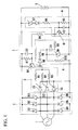
- FIG. 1 is a circuit diagram illustrating a structure of a battery charging circuit according to a first embodiment of the present invention.
- the battery charging circuit includes: a rectifier circuit 2 that rectifies a three-phase (phases U, V, and W) AC voltage outputted from an electric power generator 1 and generates a charge voltage for charging a battery B; a voltage detection circuit 4 that detects that a voltage of the battery B becomes equal to or higher than a predetermined voltage; a switching circuit 3 that charges, in an off-state, the battery B through the rectifier circuit 2, and short-circuits, in an on-state, the electric power generator 1 through the rectifier circuit 2; a switch control circuit 5 that, when the voltage detection circuit 4 detects that the voltage of the battery B becomes equal to or higher than the predetermined voltage, switches the switching circuit 3 to the on-state; and a control circuit 6 that controls the switching circuit 3 to maintain the on-state when the switching circuit 3 is in the on-state
- the electric power generator 1 generates the three-phase AC voltage for charging the battery B.
- the three-phase AC voltage includes the phases U, V, and W.
- the rectifier circuit 2 includes diodes D1 to D6.
- An anode of the diode D1 and a cathode of the diode D4 are connected to the phase U of the electric power generator 1.
- An anode of the diode D2 and a cathode of the diode D5 are connected to the phase V of the electric power generator 1.
- An anode of the diode D3 and a cathode of the diode D6 are connected to the phase W of the electric power generator 1.
- Cathodes of the diodes D1 to D3 are connected to a cathode of the battery B.
- Anodes of the diodes D4 to D6 are connected to an anode of the battery B.
- the switching circuit 3 includes thyristors S1 to S3 and the resistors R1 to R3, Anodes of the thyristors S1 to S3 are connected to the phases U, V, and W of the electric power generator 1, respectively. Cathodes of the thyristors S1 to S3 are connected to the anodes of the diodes D4 to D6, respectively. One ends of the resistors R1 to R3 are connected to gates of the thyristors S1 to S3, respectively. The other ends of the resistors R1 to R3 are connected to the switch control circuit 5 and the control circuit 6.
- the voltage detection circuit 4 includes: a zener diode ZD1, a cathode of the zener diode ZD2 being connected to the cathode of the battery B; a diode D7, an anode of the diode D7 being connected to the anode of the zener diode ZD1; a resistor R4, one end of the resistor R4 being connected to the cathode of the diode D7; a transistor Q1, a base of the transistor Q1 being connected to the other end of the resistor R4, and an emitter of the transistor Q1 being connected to the anode of the battery B; and a resistor R5 and a capacitor C2 that are connected in parallel between a base and an emitter of the transistor Q1.
- a collector of the transistor Q1 is connected to the switch control circuit 5.
- the switch control circuit 5 includes: a resistor R6, one end of the resistor R6 being connected to the collector of the transistor Q1; a transistor Q2. a base of the transistor Q2 being connected to the other end of the resistor R6, and an emitter of the transistor Q2 being connected to the cathode of the battery B; and a resistor R7 and a capacitor C3 that are connected in parallel between the base and the emitter of the transistor Q2.
- a collector of the transistor Q2 is connected to the resistors R1 to R3 in the switching circuit 3 and to the control circuit 6.
- the control circuit 6 includes: a capacitor C1; a diode D8; a zener diode ZD2; and resistors R8 to R10.
- the capacitor C1 is provided between the collector of the transistor Q2 and the base of the transistor Q1.
- the diode D8 is provided between the transistor Q2 and the capacitor C1 such that the anode of the diode D8 is connected to the collector of the transistor Q2.
- the resistor R8 is provided between the capacitor C1 and the diode D8.
- the resistor R9 is provided between the capacitor C1 and the base of the transistor Q1.
- the cathode of the zener diode ZD2 is connected to a connecting point of the capacitor C1 and the resistor R8.
- the anode of the zener diode ZD2 is connected to the anode of the battery B.
- the resistor R10 and the zener diode ZD2 are connected in parallel.
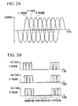
- the gate current is zero, and therefore the thyristors S1 to S3 changes to the off-state (in which a current does not flow from the anode to the cathode). Accordingly, the three-phase AC voltage outputted from the electric power generator 1 is rectified by each of the diodes D1 to D6, and the battery B is charged with the rectified voltage as a charge voltage (a charging period shown in FIG. 2B ).
- the phase U current shown in FIG. 2A flows through the diode D1, the battery B, and the diode D5.
- the phase V current shown in FIG. 2A flows through the diode D2, the battery B, and the diode D6.
- the phase W current shown in FIG. 2A flows through the diode D3, the battery B, and the diode D4.
- the battery B is charged with the charge voltage that is rectified in this manner.
- each of the thyristors S1 to S3 changes to the on-state (in which a current flows from the anode to the cathode). Therefore, the phase U of the electric power generator 1 shown in FIG. 2A is short-circuited through the thyristor S1 and the diode D5. The phase V shown in FIG. 2A is short-circuited through the thyristor S2 and the diode D6. The phase W shown in FIG. 2A is short-circuited through the thyristor S3 and the diode D4. Consequently, the battery becomes in a non-charged state (non-charging period shown in FIG. 2B ).
- the transistor Q2 changes to the on-state as explained above, the current flowing between the emitter and the collector of the transistor Q2 partially flows into the control circuit 6.
- the capacitor C1 in the control circuit 6 is charged with the current flown into the control circuit 6.
- a base potential of the transistor Q1 in the voltage detection circuit 4 is kept high, and therefore the transistor Q1 maintains the on-state. Consequently, the transistor Q2 in the switch control circuit 5 also maintains the on-state.
- each of the thyristors S1 to S3 becomes the off-state once when the AC voltage of the electric power generator 1 becomes negative.
- the transistor Q2 maintains the on-state and therefore the gate electrode flows.
- each of the thyristors S1 to 53 changes to the on-state again when the AC voltage of the electric power generator 1 becomes positive.
- each of the thyristros S1 to S3 is controlled to maintain the on-state so that the battery B maintains the non-charged state for a predetermined period (non-charging period shown in FIG. 2B ).
- the reverse current does not flow in the zener diode ZD1. Consequently, the transistor Q1 in the voltage detection circuit 4 changes to the off-state, and the transistor Q2 in the switch control circuit 5 also switches to the off-state. For this reason, the capacitor C1 in the control circuit 6 discharges the above electric charge. Accordingly, the base of the transistor Q1 in the voltage detection circuit 4 is reverse-biased. In this state, even if the reverse current flows in the zener diode ZD1 again, the transistor Q1 maintains the off-state since the base of the transistor Q1 is reverse-biased.
- the transistor Q2 in the switch control circuit 5 maintains the off-state. Therefore, there is a sufficient period of time in which the gate current of each of the thyristors S1 to S3 is zero. For this reason, each of the thyristors S1 to S3 can properly change to the off-state during that period of time. Thereafter, the transistor Q2 continuously maintains the off-state, and therefore each of the thyristors S1 to S3 maintains the off-state.
- each of the thyristors S1 to S3 is controlled so as to change from the on-state to the off-state and then maintain the off-state, while the base of the transistor Q1 in the voltage detection circuit 4 is reverse-biased, in other words, while the capacitor C1 in the control circuit 6 discharges.
- the battery B is charged in a similar manner as explained above while each of the thyristors S1 to S3 maintains the off-state.
- each of the thyristors S1 to S3 can properly change to the off-state during that period. Accordingly, a case, in which each of the thyristors S1 to S3 is always in the on-state and therefore the battery B cannot be charged, can be prevented.
- the switching circuit 3 may include switching elements of a transistor, such as MOSFET and IGBT, in lieu of the thyristors S1 to S3.
- the embodiment can be applied to a voltage stabilizing circuit for a three-phase AC generator.
Landscapes
- Engineering & Computer Science (AREA)
- Power Engineering (AREA)
- Manufacturing & Machinery (AREA)
- Chemical & Material Sciences (AREA)
- Chemical Kinetics & Catalysis (AREA)
- Electrochemistry (AREA)
- General Chemical & Material Sciences (AREA)
- Control Of Charge By Means Of Generators (AREA)
- Charge And Discharge Circuits For Batteries Or The Like (AREA)
- Secondary Cells (AREA)
- Rectifiers (AREA)
- Control Of Eletrric Generators (AREA)
Abstract
Description
- The present invention relates to a battery charging circuit that rectifies an AC (Alternate Current) voltage and charges a battery.
Priority is claimed on Japanese Patent Application No.2008-26818, filed February 6, 2008 -
FIG. 3 is a circuit diagram illustrating a structure of a conventional battery charging circuit (see, for example, Non-Patent Document 1).FIG. 4A illustrates current waveforms of an electric power generator.FIG. 4B illustrates voltage waveforms of the electric power generator. Hereinafter, an operation of the conventional battery charging circuit is explained with reference toFIGS. 3 ,4A, and 4B . - Hereinafter, a circuit operation, when a voltage VB of a battery B is low (the battery B is not sufficiently charged), specifically, when the voltage VB is lower than a predetermined voltage determined based on a breakdown voltage of a zener diode ZD1, is explained. In a voltage detection circuit 4, a reverse current (from a cathode of the battery B to an anode of the battery B) does not flow in the zener diode ZD1. For this reason, a current does not flow between a base and an emitter of a transistor Q1. Therefore, the transistor Q1 changes to the off-state. In this case, in a switch control circuit 5, a current does not flow between a base and an emitter of a transistor Q2. Therefore, the transistor Q2 also changes to the off-state. Since a gate current of each of thyristors S1 to S3 is zero in a
switching circuit 3, theswitching circuit 3 switches to the off-state (in which a current does not flow from an anode to a cathode). Accordingly, a three-phase AC voltage outputted from anelectric power generator 1 is rectified by each of diodes D1 to D6, and thus the battery B is charged with the rectified voltage as a charge voltage (FIG. 4B ). - Hereinafter, a circuit operation, when the battery B is sufficiently charged and the voltage VB thereof becomes higher than the predetermined voltage, is explained. In the voltage detection circuit 4, a reverse current from the battery B to the zener diode ZD1 flows. Accordingly, the transistor Q1 changes to the on-state, Then, a current flows between the base and the emitter of a transistor Q2 in the switch control circuit 5, and therefore the transistor Q2 also changes to the on-state. Since a gate current flows in each of the thyristors S1 to S3 through the transistor Q2 and the resistors R1 to R3, each of the thyristors S1 to S3 changes to the on-state (in which the current flows from the anode to the cathode). Therefore, the three phases of the
electric power generator 1 are short-circuited through the diodes D4 to D6, respectively. Consequently, the battery B changes to a non-charged state. - [Non-Patent Document 1] Japanese Unexamined Patent First Publication No.
H10-70851 - Among the three thyristors S1 to S3 provided for the respective three phases, the impedance differs between a phase connected to the on-state thyristor (short-circuit phase) and a phase connected to the off-state thyristor (charging phase). For this reason, a large current flows only in a path corresponding to the short-circuit phase (phase U shown in
FIG. 4A ), and a small current flows in a path corresponding to the charging phase (phases V and W shown inFIG. 4A ). For this reason, a current bias occurs among the three phases. It takes a predetermined time to change the on-state thyristor to the off-state until the thyristor changes to the off-state. For this reason, control for changing the thyristor to the next on-state might initiate before the thyristor actually changes to the off-state. In this case, the thyristor in the short-circuit phase (phase U shown inFIG. 4A ), in which a large current flows, maintains the on-state. The thyristor in the charging phase (phases V and W shown inFIG. 4A ), in which only a small current flows, maintains the off-state. In other words, the battery B is charged only in the phase in which only a small current flows (phases V and W shown inFIG. 4A ). For this reason, a problem that the battery B cannot be efficiently charged arises. - The present invention is made in view of the above situations. An object of the present invention is to provide a battery charging circuit that can properly control the switching circuit that switches charging and non-charging of the battery in order to efficiently charge the battery.
- According to a first aspect of the present invention, a battery charging circuit includes; a rectifier circuit that rectifies a three-phase alternate-current voltage outputted from an electric power generator and generates a charge voltage for charging a battery; a voltage detection circuit that detects that a voltage of the battery becomes equal to or higher than a predetermined voltage; a switching circuit that charges, in an off-state, the battery through the rectifier circuit and that short-circuits, in an on-state, the electric power generator through the rectifier circuit; a switch control circuit that switches the switching circuit to the on-state when the voltage detection circuit detects that the voltage of the battery becomes equal to or higher than the predetermined voltage; and a control circuit that controls the switching circuit to switch from the on-state to the off-state and to maintain the off-state.
- Regarding the battery charging circuit according to the first aspect of the present invention, the control circuit may include a capacitor that is charged when the switch control circuit controls the switching circuit to switch to the on-state, the capacitor discharging when the switch control circuit controls the switching circuit to switch to the off-state. The voltage detection circuit may include a first transistor, a base of the first transistor being reverse-biased by the capacitor discharging. The switch control circuit may include a second transistor, a base of the second transistor being connected to an emitter of the first transistor, the switch control circuit controlling the on-state and the off-state of the switching circuit based on a collector current through the emitter.
- According to a second aspect of the present invention, a battery charging circuit includes: a rectifier circuit that rectifies a three-phase alternate-current voltage outputted from an electric power generator and generates a charge voltage for charging a battery; a voltage detection circuit that detects that a voltage of the battery becomes equal to or higher than a predetermined voltage; a switching circuit that charges, in an off-state, the battery through the rectifier circuit and that short-circuits, in an on-state, the electric power generator through the rectifier circuit; a switch control circuit that switches the switching circuit to the on-state when the voltage detection circuit detects that the voltage of the battery becomes equal to or higher than the predetermined voltage; and a control circuit that controls the switching circuit to maintain the on-state when the switching circuit is in the on-state and to maintain the off-state when the switching circuit is in the off-state.
- According to the second aspect of the present invention, the control circuit may include a capacitor that is charged when the switch control circuit controls the switching circuit to switch to the on-state, the capacitor discharging when the switch control circuit controls the switching circuit to switch to the off-state. The voltage detection circuit may include a first transistor, a base of the first transistor being reverse-biased by the capacitor discharging. The switch control circuit may include a second transistor, a base of the second transistor being connected to an emitter of the first transistor, the switch control circuit controlling the on-state and the off-state of the switching circuit based on a collector current through the emitter.
- According to a third aspect of the present invention, there is provided a method of controlling a battery charging circuit. The battery charging circuit includes; a rectifier circuit that rectifies a three-phase alternate-current voltage outputted from an electric power generator and generates a charge voltage for charging a battery; a voltage detection circuit that detects that a voltage of the battery becomes equal to or higher than a predetermined voltage; and a switching circuit that charges, in an off-state, the battery through the rectifier circuit and that short-circuits, in an on-state, the electric power generator through the rectifier circuit. The method includes: when the voltage detection circuit detects that the voltage of the battery becomes equal to or higher than the predetermined voltage, changing the switching circuit to the on-state; and when the voltage detection circuit detects that the voltage of the battery becomes lower than the predetermined voltage, changing the switching circuit from the on-state to the off-state and making the switching circuit maintain the off-state.
- According to a fourth aspect of the present invention, there is provide a method of controlling a battery charging circuit. The battery charging circuit includes: a rectifier circuit that rectifies a three-phase alternate-current voltage outputted from an electric power generator and generates a charge voltage for charging a battery; a voltage detection circuit that detects that a voltage of the battery becomes equal to or higher than a predetermined voltage; and a switching circuit that charges, in an off-state, the battery through the rectifier circuit and that short-circuits, in an on-state, the electric power generator through the rectifier circuit. The method includes: when the voltage detection circuit detects that the voltage of the battery becomes equal to or higher than the predetermined voltage, changing the switching circuit to the on-state and making the switching circuit maintain the on-state; and when the voltage detection circuit detects that the voltage of the battery becomes lower than the predetermined voltage, changing the switching circuit from the on-state to the off-state and making the switching circuit maintain the off-state.
- According to the present invention, control for changing the switching circuit to the off-state is continuously performed. For this reason, the switching circuit can properly switch from the on-state to the off-state during the continuous control. Therefore, a case, in which the switching circuit is always in the on-state and the battery is charged only in the phase in which a small current flows, can be prevented, and the battery can be efficiently charged.
-
-
FIG. 1 is a circuit diagram illustrating a structure of a battery charging circuit according to a first embodiment of the present invention. -
FIG. 2A illustrates current waveforms of an electric power generator shown inFIG. 1 . -
FIG. 2B illustrates voltage waveforms of the electric power generator shown inFIG. 1 . -
FIG. 3 is a circuit diagram illustrating a structure of a battery charging circuit of a related art. -
FIG. 4A illustrates current waveforms of an electric power generator shown inFIG. 3 . -
FIG. 4B illustrates voltage waveforms of the electric power generator shown inFIG. 3 . -
- 1 electric power generator
- 2 rectifier circuit
- 3 switching circuit
- 4 voltage detection circuit
- 5 switch control circuit
- 6 control circuit
- B battery
- D1 to D8 diode
- S1 to S3 thyristor
- ZD1 and ZD2 zener diode
- Q1 and Q2 transistor
- R1 to R10 resistor
- C1 to C3 capacitor
- Hereinafter, embodiments of the present invention are explained in detail with reference to accompanying drawings.
FIG. 1 is a circuit diagram illustrating a structure of a battery charging circuit according to a first embodiment of the present invention. The battery charging circuit includes: arectifier circuit 2 that rectifies a three-phase (phases U, V, and W) AC voltage outputted from anelectric power generator 1 and generates a charge voltage for charging a battery B; a voltage detection circuit 4 that detects that a voltage of the battery B becomes equal to or higher than a predetermined voltage; aswitching circuit 3 that charges, in an off-state, the battery B through therectifier circuit 2, and short-circuits, in an on-state, theelectric power generator 1 through therectifier circuit 2; a switch control circuit 5 that, when the voltage detection circuit 4 detects that the voltage of the battery B becomes equal to or higher than the predetermined voltage, switches theswitching circuit 3 to the on-state; and a control circuit 6 that controls theswitching circuit 3 to maintain the on-state when theswitching circuit 3 is in the on-state and to maintain the off-state when theswitching circuit 3 is in the off-state. - The
electric power generator 1 generates the three-phase AC voltage for charging the battery B. The three-phase AC voltage includes the phases U, V, and W. - The
rectifier circuit 2 includes diodes D1 to D6. An anode of the diode D1 and a cathode of the diode D4 are connected to the phase U of theelectric power generator 1. An anode of the diode D2 and a cathode of the diode D5 are connected to the phase V of theelectric power generator 1. An anode of the diode D3 and a cathode of the diode D6 are connected to the phase W of theelectric power generator 1. Cathodes of the diodes D1 to D3 are connected to a cathode of the battery B. Anodes of the diodes D4 to D6 are connected to an anode of the battery B. - The
switching circuit 3 includes thyristors S1 to S3 and the resistors R1 to R3, Anodes of the thyristors S1 to S3 are connected to the phases U, V, and W of theelectric power generator 1, respectively. Cathodes of the thyristors S1 to S3 are connected to the anodes of the diodes D4 to D6, respectively. One ends of the resistors R1 to R3 are connected to gates of the thyristors S1 to S3, respectively. The other ends of the resistors R1 to R3 are connected to the switch control circuit 5 and the control circuit 6. - The voltage detection circuit 4 includes: a zener diode ZD1, a cathode of the zener diode ZD2 being connected to the cathode of the battery B; a diode D7, an anode of the diode D7 being connected to the anode of the zener diode ZD1; a resistor R4, one end of the resistor R4 being connected to the cathode of the diode D7; a transistor Q1, a base of the transistor Q1 being connected to the other end of the resistor R4, and an emitter of the transistor Q1 being connected to the anode of the battery B; and a resistor R5 and a capacitor C2 that are connected in parallel between a base and an emitter of the transistor Q1. A collector of the transistor Q1 is connected to the switch control circuit 5.
- The switch control circuit 5 includes: a resistor R6, one end of the resistor R6 being connected to the collector of the transistor Q1; a transistor Q2. a base of the transistor Q2 being connected to the other end of the resistor R6, and an emitter of the transistor Q2 being connected to the cathode of the battery B; and a resistor R7 and a capacitor C3 that are connected in parallel between the base and the emitter of the transistor Q2. A collector of the transistor Q2 is connected to the resistors R1 to R3 in the
switching circuit 3 and to the control circuit 6. - The control circuit 6 includes: a capacitor C1; a diode D8; a zener diode ZD2; and resistors R8 to R10. The capacitor C1 is provided between the collector of the transistor Q2 and the base of the transistor Q1. The diode D8 is provided between the transistor Q2 and the capacitor C1 such that the anode of the diode D8 is connected to the collector of the transistor Q2. The resistor R8 is provided between the capacitor C1 and the diode D8. The resistor R9 is provided between the capacitor C1 and the base of the transistor Q1. The cathode of the zener diode ZD2 is connected to a connecting point of the capacitor C1 and the resistor R8. The anode of the zener diode ZD2 is connected to the anode of the battery B. The resistor R10 and the zener diode ZD2 are connected in parallel.
- Hereinafter, an operation of the battery charging circuit having the above structure is explained with reference to the current and voltage waveforms of the
electric power generator 1 shown inFIGS. 2A and 2B , respectively. - Hereinafter, a circuit operation, when the voltage VB of the battery B is low (the battery B is not sufficiently charged), specifically, when the voltage VB is lower than a predetermined voltage determined based on a breakdown voltage of the zener diode ZD1, is explained. In the voltage detection circuit 4, a reverse current (from the cathode of the battery B to the anode of the battery B) does not flow in the zener diode ZD1. For this reason, a current does not flow between the base and the emitter of the transistor Q1. Accordingly, the transistor Q1 changes to the off-state. In this case, a current does not flow between the base and the emitter of the transistor Q2, and therefore the transistor Q2 also changes to the off-state. In the
switching circuit 3, the gate current is zero, and therefore the thyristors S1 to S3 changes to the off-state (in which a current does not flow from the anode to the cathode). Accordingly, the three-phase AC voltage outputted from theelectric power generator 1 is rectified by each of the diodes D1 to D6, and the battery B is charged with the rectified voltage as a charge voltage (a charging period shown inFIG. 2B ). In other words, the phase U current shown inFIG. 2A flows through the diode D1, the battery B, and the diode D5. The phase V current shown inFIG. 2A flows through the diode D2, the battery B, and the diode D6. The phase W current shown inFIG. 2A flows through the diode D3, the battery B, and the diode D4. The battery B is charged with the charge voltage that is rectified in this manner. - Hereinafter, a circuit operation, when the battery B is sufficiently charged and the voltage VB thereof becomes higher than the predetermined voltage, is explained. In the voltage detection circuit 4, a reverse current from the battery B to the zener diode ZD1 flows. Consequently, the transistor Q1 changes to the on-state. Then, in the switch control circuit 5, a current flows between the base and the emitter of the transistor Q2, and therefore the transistor Q2 also changes to the on-state. In the
switching circuit 3, a gate current flows in each of the thyristors S1 to S3 through the transistor Q2 and the resistors R1 to R3. Accordingly, each of the thyristors S1 to S3 changes to the on-state (in which a current flows from the anode to the cathode). Therefore, the phase U of theelectric power generator 1 shown inFIG. 2A is short-circuited through the thyristor S1 and the diode D5. The phase V shown inFIG. 2A is short-circuited through the thyristor S2 and the diode D6. The phase W shown inFIG. 2A is short-circuited through the thyristor S3 and the diode D4. Consequently, the battery becomes in a non-charged state (non-charging period shown inFIG. 2B ). - Further, when the transistor Q2 changes to the on-state as explained above, the current flowing between the emitter and the collector of the transistor Q2 partially flows into the control circuit 6. The capacitor C1 in the control circuit 6 is charged with the current flown into the control circuit 6. When the capacitor C1 is charged, a base potential of the transistor Q1 in the voltage detection circuit 4 is kept high, and therefore the transistor Q1 maintains the on-state. Consequently, the transistor Q2 in the switch control circuit 5 also maintains the on-state. In this case, each of the thyristors S1 to S3 becomes the off-state once when the AC voltage of the
electric power generator 1 becomes negative. However, the transistor Q2 maintains the on-state and therefore the gate electrode flows. Consequently, each of the thyristors S1 to 53 changes to the on-state again when the AC voltage of theelectric power generator 1 becomes positive. Thus, each of the thyristros S1 to S3 is controlled to maintain the on-state so that the battery B maintains the non-charged state for a predetermined period (non-charging period shown inFIG. 2B ). - Then, when the electric power of the battery B is consumed by an external circuit (not shown) and the like, and the voltage VB of the battery B becomes lower than the predetermined voltage again, the reverse current does not flow in the zener diode ZD1. Consequently, the transistor Q1 in the voltage detection circuit 4 changes to the off-state, and the transistor Q2 in the switch control circuit 5 also switches to the off-state. For this reason, the capacitor C1 in the control circuit 6 discharges the above electric charge. Accordingly, the base of the transistor Q1 in the voltage detection circuit 4 is reverse-biased. In this state, even if the reverse current flows in the zener diode ZD1 again, the transistor Q1 maintains the off-state since the base of the transistor Q1 is reverse-biased. Consequently, the transistor Q2 in the switch control circuit 5 maintains the off-state. Therefore, there is a sufficient period of time in which the gate current of each of the thyristors S1 to S3 is zero. For this reason, each of the thyristors S1 to S3 can properly change to the off-state during that period of time. Thereafter, the transistor Q2 continuously maintains the off-state, and therefore each of the thyristors S1 to S3 maintains the off-state. Thus, each of the thyristors S1 to S3 is controlled so as to change from the on-state to the off-state and then maintain the off-state, while the base of the transistor Q1 in the voltage detection circuit 4 is reverse-biased, in other words, while the capacitor C1 in the control circuit 6 discharges. The battery B is charged in a similar manner as explained above while each of the thyristors S1 to S3 maintains the off-state.
- Thus, the transistor Q2 maintains the off-state while the capacitor C1 discharges. Therefore, each of the thyristors S1 to S3 can properly change to the off-state during that period. Accordingly, a case, in which each of the thyristors S1 to S3 is always in the on-state and therefore the battery B cannot be charged, can be prevented.
- Although an embodiment of the present invention has been explained in detail with reference to the accompanying drawings, the specific structure of the present invention is not limited thereto, and may be modified and changed without departing from the scope of the invention.
For example, the switchingcircuit 3 may include switching elements of a transistor, such as MOSFET and IGBT, in lieu of the thyristors S1 to S3. - Although the battery charging circuit using the three-phase AC generator has been taken as an example for explaining the embodiment, the embodiment can be applied to a voltage stabilizing circuit for a three-phase AC generator.
Claims (6)
- A battery charging circuit comprising:a rectifier circuit that rectifies a three-phase alternate-current voltage outputted from an electric power generator and generates a charge voltage for charging a battery;a voltage detection circuit that detects that a voltage of the battery becomes equal to or higher than a predetermined voltage;a switching circuit that charges, in an off-state, the battery through the rectifier circuit and that short-circuits, in an on-state, the electric power generator through the rectifier circuit;a switch control circuit that switches the switching circuit to the on-state when the voltage detection circuit detects that the voltage of the battery becomes equal to or higher than the predetermined voltage; anda control circuit that controls the switching circuit to switch from the on-state to the off-state and to maintain the off-state.
- The battery charging circuit according to claim 1, wherein
the control circuit comprises a capacitor that is charged when the switch control circuit controls the switching circuit to switch to the on-state, the capacitor discharging when the switch control circuit controls the switching circuit to switch to the off-state,
the voltage detection circuit comprises a first transistor, a base of the first transistor being reverse-biased by the capacitor discharging, and
the switch control circuit comprises a second transistor, a base of the second transistor being connected to an emitter of the first transistor, the switch control circuit controlling the on-state and the off-state of the switching circuit based on a collector current through the emitter. - A battery charging circuit comprising:a rectifier circuit that rectifies a three-phase alternate-current voltage outputted from an electric power generator and generates a charge voltage for charging a battery;a voltage detection circuit that detects that a voltage of the battery becomes equal to or higher than a predetermined voltage;a switching circuit that charges, in an off-state, the battery through the rectifier circuit and that short-circuits, in an on-state, the electric power generator through the rectifier circuit;a switch control circuit that switches the switching circuit to the on-state when the voltage detection circuit detects that the voltage of the battery becomes equal to or higher than the predetermined voltage; anda control circuit that controls the switching circuit to maintain the on-state when the switching circuit is in the on-state and to maintain the off-state when the switching circuit is in the off-state.
- The battery charging circuit according to claim 3, wherein
the control circuit comprises a capacitor that is charged when the switch control circuit controls the switching circuit to switch to the on-state, the capacitor discharging when the switch control circuit controls the switching circuit to switch to the off-state,
the voltage detection circuit comprises a first transistor, a base of the first transistor being reverse-biased by the capacitor discharging, and
the switch control circuit comprises a second transistor, a base of the second transistor being connected to an emitter of the first transistor, the switch control circuit controlling the on-state and the off-state of the switching circuit based on a collector current through the emitter. - A method of controlling a battery charging circuit, the battery charging circuit comprising: a rectifier circuit that rectifies a three-phase alternate-current voltage outputted from an electric power generator and generates a charge voltage for charging a battery; a voltage detection circuit that detects that a voltage of the battery becomes equal to or higher than a predetermined voltage; and a switching circuit that charges, in an off-state, the battery through the rectifier circuit and that short-circuits, in an on-state, the electric power generator through the rectifier circuit, the method comprising:when the voltage detection circuit detects that the voltage of the battery becomes equal to or higher than the predetermined voltage, changing the switching circuit to the on-state; andwhen the voltage detection circuit detects that the voltage of the battery becomes lower than the predetermined voltage, changing the switching circuit from the on-state to the off-state and making the switching circuit maintain the off-state.
- A method of controlling a battery charging circuit, the battery charging circuit comprising: a rectifier circuit that rectifies a three-phase alternate-current voltage outputted from an electric power generator and generates a charge voltage for charging a battery; a voltage detection circuit that detects that a voltage of the battery becomes equal to or higher than a predetermined voltage; and a switching circuit that charges, in an off-state, the battery through the rectifier circuit and that short-circuits, in an on-state, the electric power generator through the rectifier circuit, the method comprising:when the voltage detection circuit detects that the voltage of the battery becomes equal to or higher than the predetermined voltage, changing the switching circuit to the on-state and making the switching circuit maintain the on-state; andwhen the voltage detection circuit detects that the voltage of the battery becomes lower than the predetermined voltage, changing the switching circuit from the on-state to the off-state and making the switching circuit maintain the off-state.
Applications Claiming Priority (2)
| Application Number | Priority Date | Filing Date | Title |
|---|---|---|---|
| JP2008026818A JP5032357B2 (en) | 2008-02-06 | 2008-02-06 | Battery charging circuit |
| PCT/JP2009/051966 WO2009099144A1 (en) | 2008-02-06 | 2009-02-05 | Battery charging circuit |
Publications (3)
| Publication Number | Publication Date |
|---|---|
| EP2242162A1 true EP2242162A1 (en) | 2010-10-20 |
| EP2242162A4 EP2242162A4 (en) | 2017-03-29 |
| EP2242162B1 EP2242162B1 (en) | 2018-08-29 |
Family
ID=40952217
Family Applications (1)
| Application Number | Title | Priority Date | Filing Date |
|---|---|---|---|
| EP09708915.5A Active EP2242162B1 (en) | 2008-02-06 | 2009-02-05 | Battery charging circuit |
Country Status (6)
| Country | Link |
|---|---|
| US (1) | US8415929B2 (en) |
| EP (1) | EP2242162B1 (en) |
| JP (1) | JP5032357B2 (en) |
| CN (1) | CN101933213B (en) |
| TW (1) | TWI376859B (en) |
| WO (1) | WO2009099144A1 (en) |
Families Citing this family (9)
| Publication number | Priority date | Publication date | Assignee | Title |
|---|---|---|---|---|
| JP5295193B2 (en) * | 2010-09-24 | 2013-09-18 | 三菱電機株式会社 | Power supply |
| JP5722190B2 (en) * | 2011-10-21 | 2015-05-20 | 新電元工業株式会社 | Battery charging circuit, battery charging system, and battery charging circuit control method |
| JP5744700B2 (en) * | 2011-10-21 | 2015-07-08 | 新電元工業株式会社 | Battery charging circuit, battery charging system, and battery charging circuit control method |
| JP5415630B2 (en) * | 2011-12-13 | 2014-02-12 | 新電元工業株式会社 | Regulator, battery charging device, and battery charging method |
| US9425608B2 (en) * | 2011-12-20 | 2016-08-23 | Kohler Co. | Overvoltage protection system and method |
| US20150248152A1 (en) * | 2014-02-28 | 2015-09-03 | International Business Machines Corporation | Battery with integrated power timer |
| KR102237376B1 (en) * | 2016-09-08 | 2021-04-06 | 삼성에스디아이 주식회사 | Battery pack |
| KR102256094B1 (en) | 2017-11-28 | 2021-05-25 | 주식회사 엘지에너지솔루션 | Battery back |
| CN113178936B (en) * | 2021-04-28 | 2022-08-23 | 合肥工业大学 | Public domain microgrid system for multi-energy complementary power generation |
Family Cites Families (18)
| Publication number | Priority date | Publication date | Assignee | Title |
|---|---|---|---|---|
| US5686815A (en) * | 1991-02-14 | 1997-11-11 | Chartec Laboratories A/S | Method and apparatus for controlling the charging of a rechargeable battery to ensure that full charge is achieved without damaging the battery |
| JP3099405B2 (en) * | 1991-04-24 | 2000-10-16 | 株式会社デンソー | Power supply for vehicles |
| JP3577174B2 (en) | 1996-08-26 | 2004-10-13 | 新電元工業株式会社 | Battery charger |
| JP3409659B2 (en) * | 1997-09-03 | 2003-05-26 | 国産電機株式会社 | Battery charger powered by a magnet type alternator |
| JP2000278897A (en) | 1999-03-24 | 2000-10-06 | Toyoda Mach Works Ltd | Motor |
| KR100341986B1 (en) * | 1999-04-23 | 2002-06-26 | 윤종용 | Battery Charger And Charge Control Method |
| US6215271B1 (en) * | 1999-05-11 | 2001-04-10 | Satcon Technology Corporation | Charging system having a controlled rectifier bridge and a single voltage sensor |
| JP3489523B2 (en) * | 2000-02-16 | 2004-01-19 | 国産電機株式会社 | Battery charger |
| JP3491683B2 (en) * | 2000-03-07 | 2004-01-26 | 国産電機株式会社 | Battery charger |
| US7012405B2 (en) * | 2001-09-14 | 2006-03-14 | Ricoh Company, Ltd. | Charging circuit for secondary battery |
| JP3637887B2 (en) * | 2001-10-02 | 2005-04-13 | 国産電機株式会社 | Battery charge control device |
| US7345450B2 (en) * | 2002-02-19 | 2008-03-18 | V Ector Products, Inc. | Microprocessor controlled booster apparatus with polarity protection |
| JP4497404B2 (en) | 2004-05-25 | 2010-07-07 | 本田技研工業株式会社 | Portable generator |
| US7098629B2 (en) | 2004-05-25 | 2006-08-29 | Honda Motor Co., Ltd. | Generator apparatus |
| TWI283097B (en) * | 2004-12-31 | 2007-06-21 | Jason Auto Technology Co Ltd | Method and device for battery charger and diagnosis with detectable battery energy barrier |
| JP4367416B2 (en) * | 2006-01-13 | 2009-11-18 | 国産電機株式会社 | Battery charge control device |
| CN200944534Y (en) | 2006-05-18 | 2007-09-05 | 世阳企业股份有限公司 | Generator power charge and discharge control and protection device |
| JP4486618B2 (en) * | 2006-06-06 | 2010-06-23 | 株式会社リコー | Charging circuit, charging circuit operation control method, and power supply device |
-
2008
- 2008-02-06 JP JP2008026818A patent/JP5032357B2/en active Active
-
2009
- 2009-02-04 TW TW098103561A patent/TWI376859B/en active
- 2009-02-05 WO PCT/JP2009/051966 patent/WO2009099144A1/en not_active Ceased
- 2009-02-05 US US12/865,941 patent/US8415929B2/en active Active
- 2009-02-05 CN CN200980103889.3A patent/CN101933213B/en active Active
- 2009-02-05 EP EP09708915.5A patent/EP2242162B1/en active Active
Also Published As
| Publication number | Publication date |
|---|---|
| US20100327817A1 (en) | 2010-12-30 |
| EP2242162B1 (en) | 2018-08-29 |
| EP2242162A4 (en) | 2017-03-29 |
| JP5032357B2 (en) | 2012-09-26 |
| TWI376859B (en) | 2012-11-11 |
| TW200950261A (en) | 2009-12-01 |
| JP2009189160A (en) | 2009-08-20 |
| US8415929B2 (en) | 2013-04-09 |
| WO2009099144A1 (en) | 2009-08-13 |
| CN101933213A (en) | 2010-12-29 |
| CN101933213B (en) | 2014-03-19 |
Similar Documents
| Publication | Publication Date | Title |
|---|---|---|
| EP2242162A1 (en) | Battery charging circuit | |
| US9787193B2 (en) | Switching power supply and method for controlling voltage of bulk capacitor in the switching power supply | |
| EP2560282A1 (en) | Gate drive circuit | |
| CN109643955B (en) | Switching power supply device and semiconductor device | |
| KR102482820B1 (en) | Insulated switching power supply | |
| JP2016158478A (en) | Semiconductor element driving device | |
| US12206401B2 (en) | Drive device to drive semiconductor element, semiconductor device, and power conversion device | |
| JP2002281737A (en) | IGBT series connected gate drive circuit | |
| JP4850009B2 (en) | Matrix converter | |
| JP5415630B2 (en) | Regulator, battery charging device, and battery charging method | |
| CN111030225A (en) | A bidirectional power supply device and its control method | |
| JP6953885B2 (en) | Power supply and cutoff switch circuit | |
| JP2015226445A (en) | Charger | |
| CN210536518U (en) | High-voltage auxiliary power supply and high-voltage auxiliary power supply control system | |
| CN209767182U (en) | Battery protection circuit | |
| US8841887B2 (en) | Power supply device | |
| JP5739014B1 (en) | Battery charging device and battery charging device control method | |
| JP2012095458A (en) | Power supply unit and power tool having the same | |
| JP2018098940A (en) | Initial charger and load driving system | |
| US10012199B2 (en) | Power conversion device | |
| KR20150001621A (en) | Start-up circuit, switch control circuit comprising the start-up circuit and power supply device comprsing the switch control circuit | |
| JP2006166609A (en) | Battery charger | |
| JP2011234476A (en) | Switching power supply | |
| JP2006101620A (en) | Battery charger | |
| KR20160062484A (en) | Chopper circuit of converter |
Legal Events
| Date | Code | Title | Description |
|---|---|---|---|
| PUAI | Public reference made under article 153(3) epc to a published international application that has entered the european phase |
Free format text: ORIGINAL CODE: 0009012 |
|
| 17P | Request for examination filed |
Effective date: 20100804 |
|
| AK | Designated contracting states |
Kind code of ref document: A1 Designated state(s): AT BE BG CH CY CZ DE DK EE ES FI FR GB GR HR HU IE IS IT LI LT LU LV MC MK MT NL NO PL PT RO SE SI SK TR |
|
| AX | Request for extension of the european patent |
Extension state: AL BA RS |
|
| DAX | Request for extension of the european patent (deleted) | ||
| RA4 | Supplementary search report drawn up and despatched (corrected) |
Effective date: 20170301 |
|
| RIC1 | Information provided on ipc code assigned before grant |
Ipc: H02M 7/12 20060101ALI20170223BHEP Ipc: H02J 7/14 20060101AFI20170223BHEP Ipc: H01M 10/44 20060101ALI20170223BHEP |
|
| GRAP | Despatch of communication of intention to grant a patent |
Free format text: ORIGINAL CODE: EPIDOSNIGR1 |
|
| STAA | Information on the status of an ep patent application or granted ep patent |
Free format text: STATUS: GRANT OF PATENT IS INTENDED |
|
| INTG | Intention to grant announced |
Effective date: 20180522 |
|
| RIN1 | Information on inventor provided before grant (corrected) |
Inventor name: TABUTA, MAKOTO |
|
| GRAS | Grant fee paid |
Free format text: ORIGINAL CODE: EPIDOSNIGR3 |
|
| GRAA | (expected) grant |
Free format text: ORIGINAL CODE: 0009210 |
|
| STAA | Information on the status of an ep patent application or granted ep patent |
Free format text: STATUS: THE PATENT HAS BEEN GRANTED |
|
| RIN1 | Information on inventor provided before grant (corrected) |
Inventor name: TABUTA, MAKOTO |
|
| AK | Designated contracting states |
Kind code of ref document: B1 Designated state(s): AT BE BG CH CY CZ DE DK EE ES FI FR GB GR HR HU IE IS IT LI LT LU LV MC MK MT NL NO PL PT RO SE SI SK TR |
|
| REG | Reference to a national code |
Ref country code: GB Ref legal event code: FG4D |
|
| REG | Reference to a national code |
Ref country code: CH Ref legal event code: EP |
|
| REG | Reference to a national code |
Ref country code: AT Ref legal event code: REF Ref document number: 1036295 Country of ref document: AT Kind code of ref document: T Effective date: 20180915 |
|
| REG | Reference to a national code |
Ref country code: IE Ref legal event code: FG4D |
|
| REG | Reference to a national code |
Ref country code: DE Ref legal event code: R096 Ref document number: 602009054147 Country of ref document: DE |
|
| REG | Reference to a national code |
Ref country code: NL Ref legal event code: MP Effective date: 20180829 |
|
| REG | Reference to a national code |
Ref country code: LT Ref legal event code: MG4D |
|
| PG25 | Lapsed in a contracting state [announced via postgrant information from national office to epo] |
Ref country code: LT Free format text: LAPSE BECAUSE OF FAILURE TO SUBMIT A TRANSLATION OF THE DESCRIPTION OR TO PAY THE FEE WITHIN THE PRESCRIBED TIME-LIMIT Effective date: 20180829 Ref country code: NL Free format text: LAPSE BECAUSE OF FAILURE TO SUBMIT A TRANSLATION OF THE DESCRIPTION OR TO PAY THE FEE WITHIN THE PRESCRIBED TIME-LIMIT Effective date: 20180829 Ref country code: BG Free format text: LAPSE BECAUSE OF FAILURE TO SUBMIT A TRANSLATION OF THE DESCRIPTION OR TO PAY THE FEE WITHIN THE PRESCRIBED TIME-LIMIT Effective date: 20181129 Ref country code: SE Free format text: LAPSE BECAUSE OF FAILURE TO SUBMIT A TRANSLATION OF THE DESCRIPTION OR TO PAY THE FEE WITHIN THE PRESCRIBED TIME-LIMIT Effective date: 20180829 Ref country code: GR Free format text: LAPSE BECAUSE OF FAILURE TO SUBMIT A TRANSLATION OF THE DESCRIPTION OR TO PAY THE FEE WITHIN THE PRESCRIBED TIME-LIMIT Effective date: 20181130 Ref country code: NO Free format text: LAPSE BECAUSE OF FAILURE TO SUBMIT A TRANSLATION OF THE DESCRIPTION OR TO PAY THE FEE WITHIN THE PRESCRIBED TIME-LIMIT Effective date: 20181129 Ref country code: FI Free format text: LAPSE BECAUSE OF FAILURE TO SUBMIT A TRANSLATION OF THE DESCRIPTION OR TO PAY THE FEE WITHIN THE PRESCRIBED TIME-LIMIT Effective date: 20180829 Ref country code: IS Free format text: LAPSE BECAUSE OF FAILURE TO SUBMIT A TRANSLATION OF THE DESCRIPTION OR TO PAY THE FEE WITHIN THE PRESCRIBED TIME-LIMIT Effective date: 20181229 |
|
| PG25 | Lapsed in a contracting state [announced via postgrant information from national office to epo] |
Ref country code: HR Free format text: LAPSE BECAUSE OF FAILURE TO SUBMIT A TRANSLATION OF THE DESCRIPTION OR TO PAY THE FEE WITHIN THE PRESCRIBED TIME-LIMIT Effective date: 20180829 Ref country code: ES Free format text: LAPSE BECAUSE OF FAILURE TO SUBMIT A TRANSLATION OF THE DESCRIPTION OR TO PAY THE FEE WITHIN THE PRESCRIBED TIME-LIMIT Effective date: 20180829 Ref country code: LV Free format text: LAPSE BECAUSE OF FAILURE TO SUBMIT A TRANSLATION OF THE DESCRIPTION OR TO PAY THE FEE WITHIN THE PRESCRIBED TIME-LIMIT Effective date: 20180829 |
|
| PG25 | Lapsed in a contracting state [announced via postgrant information from national office to epo] |
Ref country code: CZ Free format text: LAPSE BECAUSE OF FAILURE TO SUBMIT A TRANSLATION OF THE DESCRIPTION OR TO PAY THE FEE WITHIN THE PRESCRIBED TIME-LIMIT Effective date: 20180829 Ref country code: RO Free format text: LAPSE BECAUSE OF FAILURE TO SUBMIT A TRANSLATION OF THE DESCRIPTION OR TO PAY THE FEE WITHIN THE PRESCRIBED TIME-LIMIT Effective date: 20180829 Ref country code: EE Free format text: LAPSE BECAUSE OF FAILURE TO SUBMIT A TRANSLATION OF THE DESCRIPTION OR TO PAY THE FEE WITHIN THE PRESCRIBED TIME-LIMIT Effective date: 20180829 Ref country code: PL Free format text: LAPSE BECAUSE OF FAILURE TO SUBMIT A TRANSLATION OF THE DESCRIPTION OR TO PAY THE FEE WITHIN THE PRESCRIBED TIME-LIMIT Effective date: 20180829 |
|
| PG25 | Lapsed in a contracting state [announced via postgrant information from national office to epo] |
Ref country code: SK Free format text: LAPSE BECAUSE OF FAILURE TO SUBMIT A TRANSLATION OF THE DESCRIPTION OR TO PAY THE FEE WITHIN THE PRESCRIBED TIME-LIMIT Effective date: 20180829 Ref country code: DK Free format text: LAPSE BECAUSE OF FAILURE TO SUBMIT A TRANSLATION OF THE DESCRIPTION OR TO PAY THE FEE WITHIN THE PRESCRIBED TIME-LIMIT Effective date: 20180829 |
|
| REG | Reference to a national code |
Ref country code: DE Ref legal event code: R097 Ref document number: 602009054147 Country of ref document: DE |
|
| PLBE | No opposition filed within time limit |
Free format text: ORIGINAL CODE: 0009261 |
|
| STAA | Information on the status of an ep patent application or granted ep patent |
Free format text: STATUS: NO OPPOSITION FILED WITHIN TIME LIMIT |
|
| 26N | No opposition filed |
Effective date: 20190531 |
|
| PG25 | Lapsed in a contracting state [announced via postgrant information from national office to epo] |
Ref country code: SI Free format text: LAPSE BECAUSE OF FAILURE TO SUBMIT A TRANSLATION OF THE DESCRIPTION OR TO PAY THE FEE WITHIN THE PRESCRIBED TIME-LIMIT Effective date: 20180829 |
|
| REG | Reference to a national code |
Ref country code: CH Ref legal event code: PL |
|
| PG25 | Lapsed in a contracting state [announced via postgrant information from national office to epo] |
Ref country code: LU Free format text: LAPSE BECAUSE OF NON-PAYMENT OF DUE FEES Effective date: 20190205 Ref country code: MC Free format text: LAPSE BECAUSE OF FAILURE TO SUBMIT A TRANSLATION OF THE DESCRIPTION OR TO PAY THE FEE WITHIN THE PRESCRIBED TIME-LIMIT Effective date: 20180829 |
|
| REG | Reference to a national code |
Ref country code: BE Ref legal event code: MM Effective date: 20190228 |
|
| REG | Reference to a national code |
Ref country code: IE Ref legal event code: MM4A |
|
| PG25 | Lapsed in a contracting state [announced via postgrant information from national office to epo] |
Ref country code: CH Free format text: LAPSE BECAUSE OF NON-PAYMENT OF DUE FEES Effective date: 20190228 Ref country code: LI Free format text: LAPSE BECAUSE OF NON-PAYMENT OF DUE FEES Effective date: 20190228 |
|
| PG25 | Lapsed in a contracting state [announced via postgrant information from national office to epo] |
Ref country code: IE Free format text: LAPSE BECAUSE OF NON-PAYMENT OF DUE FEES Effective date: 20190205 |
|
| PG25 | Lapsed in a contracting state [announced via postgrant information from national office to epo] |
Ref country code: FR Free format text: LAPSE BECAUSE OF NON-PAYMENT OF DUE FEES Effective date: 20190228 Ref country code: BE Free format text: LAPSE BECAUSE OF NON-PAYMENT OF DUE FEES Effective date: 20190228 |
|
| PG25 | Lapsed in a contracting state [announced via postgrant information from national office to epo] |
Ref country code: TR Free format text: LAPSE BECAUSE OF FAILURE TO SUBMIT A TRANSLATION OF THE DESCRIPTION OR TO PAY THE FEE WITHIN THE PRESCRIBED TIME-LIMIT Effective date: 20180829 |
|
| PG25 | Lapsed in a contracting state [announced via postgrant information from national office to epo] |
Ref country code: MT Free format text: LAPSE BECAUSE OF NON-PAYMENT OF DUE FEES Effective date: 20190205 Ref country code: PT Free format text: LAPSE BECAUSE OF FAILURE TO SUBMIT A TRANSLATION OF THE DESCRIPTION OR TO PAY THE FEE WITHIN THE PRESCRIBED TIME-LIMIT Effective date: 20181229 |
|
| REG | Reference to a national code |
Ref country code: AT Ref legal event code: UEP Ref document number: 1036295 Country of ref document: AT Kind code of ref document: T Effective date: 20180829 |
|
| PG25 | Lapsed in a contracting state [announced via postgrant information from national office to epo] |
Ref country code: CY Free format text: LAPSE BECAUSE OF FAILURE TO SUBMIT A TRANSLATION OF THE DESCRIPTION OR TO PAY THE FEE WITHIN THE PRESCRIBED TIME-LIMIT Effective date: 20180829 |
|
| PG25 | Lapsed in a contracting state [announced via postgrant information from national office to epo] |
Ref country code: HU Free format text: LAPSE BECAUSE OF FAILURE TO SUBMIT A TRANSLATION OF THE DESCRIPTION OR TO PAY THE FEE WITHIN THE PRESCRIBED TIME-LIMIT; INVALID AB INITIO Effective date: 20090205 |
|
| PG25 | Lapsed in a contracting state [announced via postgrant information from national office to epo] |
Ref country code: MK Free format text: LAPSE BECAUSE OF FAILURE TO SUBMIT A TRANSLATION OF THE DESCRIPTION OR TO PAY THE FEE WITHIN THE PRESCRIBED TIME-LIMIT Effective date: 20180829 |
|
| PGFP | Annual fee paid to national office [announced via postgrant information from national office to epo] |
Ref country code: GB Payment date: 20260226 Year of fee payment: 18 |
|
| PGFP | Annual fee paid to national office [announced via postgrant information from national office to epo] |
Ref country code: DE Payment date: 20260225 Year of fee payment: 18 |
|
| PGFP | Annual fee paid to national office [announced via postgrant information from national office to epo] |
Ref country code: AT Payment date: 20260223 Year of fee payment: 18 |
|
| PGFP | Annual fee paid to national office [announced via postgrant information from national office to epo] |
Ref country code: IT Payment date: 20260227 Year of fee payment: 18 |