EP2239665A1 - Distributed flash memory storage manager systems - Google Patents
Distributed flash memory storage manager systems Download PDFInfo
- Publication number
- EP2239665A1 EP2239665A1 EP10159218A EP10159218A EP2239665A1 EP 2239665 A1 EP2239665 A1 EP 2239665A1 EP 10159218 A EP10159218 A EP 10159218A EP 10159218 A EP10159218 A EP 10159218A EP 2239665 A1 EP2239665 A1 EP 2239665A1
- Authority
- EP
- European Patent Office
- Prior art keywords
- block
- circuitry
- memory
- node
- ics
- Prior art date
- Legal status (The legal status is an assumption and is not a legal conclusion. Google has not performed a legal analysis and makes no representation as to the accuracy of the status listed.)
- Granted
Links
Images








Classifications
-
- G—PHYSICS
- G06—COMPUTING OR CALCULATING; COUNTING
- G06F—ELECTRIC DIGITAL DATA PROCESSING
- G06F12/00—Accessing, addressing or allocating within memory systems or architectures
- G06F12/02—Addressing or allocation; Relocation
- G06F12/0223—User address space allocation, e.g. contiguous or non contiguous base addressing
- G06F12/0284—Multiple user address space allocation, e.g. using different base addresses
-
- G—PHYSICS
- G06—COMPUTING OR CALCULATING; COUNTING
- G06F—ELECTRIC DIGITAL DATA PROCESSING
- G06F12/00—Accessing, addressing or allocating within memory systems or architectures
- G06F12/02—Addressing or allocation; Relocation
- G06F12/06—Addressing a physical block of locations, e.g. base addressing, module addressing, memory dedication
- G06F12/0646—Configuration or reconfiguration
- G06F12/0692—Multiconfiguration, e.g. local and global addressing
-
- G—PHYSICS
- G06—COMPUTING OR CALCULATING; COUNTING
- G06F—ELECTRIC DIGITAL DATA PROCESSING
- G06F2212/00—Indexing scheme relating to accessing, addressing or allocation within memory systems or architectures
- G06F2212/10—Providing a specific technical effect
- G06F2212/1041—Resource optimization
-
- G—PHYSICS
- G06—COMPUTING OR CALCULATING; COUNTING
- G06F—ELECTRIC DIGITAL DATA PROCESSING
- G06F2212/00—Indexing scheme relating to accessing, addressing or allocation within memory systems or architectures
- G06F2212/20—Employing a main memory using a specific memory technology
- G06F2212/202—Non-volatile memory
- G06F2212/2022—Flash memory
Definitions
- a plurality of memory circuits may each be connected to a respective one of a plurality of integrated circuits ("ICs").
- ICs integrated circuits
- Each of the ICs may be connected to at least one other of the ICs by inter-IC connections so that an IC exchanges memory circuit data with another IC via the inter-IC connections.
- Each of the ICs may include memory manager circuitry that comprises a logic block manager for maintaining a unique global identification ("ID") for each block of data contained in any portion of any of the memory circuits, the global ID including a node ID identifying the IC that is connected to the memory circuit containing that block and a logical block number for that block.
- ID unique global identification
- the memory manager circuitry for each IC may further comprise a translator for maintaining a mapping between (1) the logical block number of each block contained in the memory circuit connected to the IC that includes that translator, and (2) a physical portion ID of a portion of that memory circuit that contains that block.
- the memory manager for each IC may still further comprise a driver for receiving the physical portion ID from the translator of the IC that includes that driver and accessing the portion of the memory connected to that IC that is identified by that physical portion ID.
- each of the ICs may include circuitry for transferring a block (“the transferred block") accessed by the driver of the source IC to another of the ICs (“the destination IC”) for storage in the memory circuitry connected to the destination IC.
- the circuitry for transferring may employ the inter-IC connections.
- each of the ICs may further include circuitry for maintaining a count of how many times each of the other ICs requests a respective block contained in the memory circuit that is connected to the source IC, and circuitry for the transferring a block (“the transferred block") (for which the count for one of the other ICs (“the destination IC") exceeds a threshold value) from the memory circuit connected to the source IC to the memory circuit connected to the destination IC.
- Still other possible aspects of the disclosure relate to managing access to a plurality of memory circuits, each of which is connected to a respective one of a plurality of integrated circuits ("ICs").
- One of the ICs may be connected to at least one of the other ICs by inter-IC connections so that one IC exchanges blocks of memory circuit data with another IC via the inter-IC connections, each of the ICs ("the source IC") including a memory manager.
- Each such memory manager may comprise circuitry for maintaining a count of how many times a given IC requests at least one block contained in the memory circuit that is connected to the source IC, and circuitry for transferring a block ("the transferred block") (for which the count for one of the other ICs ("the destination IC") exceeds a threshold value) from the memory circuit connected to the source IC to the memory circuit connected to the destination IC.
- circuitry for transferring may employ the inter-IC connections.
- FIG. 1 is a simplified schematic block diagram of an illustrative embodiment of circuitry in accordance with this disclosure.
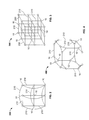
- FIG. 2 is a simplified logical diagram of an example of a system topology in accordance with the disclosure.
- FIG. 3 is similar to FIG. 2 for another illustrative system topology in accordance with the disclosure.
- FIG. 4 is similar to FIG. 2 for yet another illustrative system topology in accordance with the disclosure.
- FIG. 5 is a more detailed (but still simplified) schematic block diagram of an illustrative embodiment of a portion of the FIG. 1 circuitry in accordance with the disclosure.
- FIG. 6 is a simplified diagram of an illustrative embodiment of a data packet in accordance with the disclosure.
- FIG. 7 is similar to FIG. 5 , but shows an illustrative embodiment of more possible details in accordance with the disclosure.
- FIG. 8 is again similar to FIG. 5 , but shows an illustrative embodiment of still more possible details in accordance with the disclosure.
- FIG. 9 is a simplified schematic block diagram of an illustrative embodiment of a system (or a representative portion of a system) in accordance with the disclosure.
- FIG. 10 is a simplified schematic block diagram of an illustrative embodiment of a portion of the FIG. 1 circuitry in accordance with the disclosure.
- FIG. 11 is a simplified schematic block diagram of an another illustrative embodiment of a portion of the FIG. 1 circuitry in accordance with the disclosure.
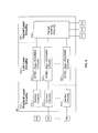
- FIG. 12 is a simplified block diagram of an illustrative embodiment of several elements in accordance with certain possible aspects of the disclosure.
- FIGS. 13a and 13b are a simplified flow chart of an illustrative embodiment of certain possible method aspects of the disclosure.
- FIGS. 14a-c are a simplified flow chart of an illustrative embodiment of certain other possible method aspects of the disclosure.
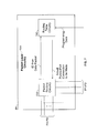
- FIGS. 15a-c are a simplified schematic block diagram of an illustrative embodiment of circuitry in accordance with certain possible aspects of the disclosure.
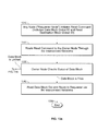
- FIGS. 16a-c are a simplified flow chart of certain, still other possible method aspects of the disclosure.
- FIGS. 1-11 herein are repeated from the Zhou et al. reference and are briefly described below. More detailed description is contained in the text of the Zhou et al. reference.
- FIG. 1 shows an illustrative embodiment of an integrated circuit ("IC") 10 that can be used as part of a distributed electronic data storage or memory system in accordance with this disclosure.
- IC integrated circuit
- an "IC” may include one or more processors with or without software that runs in and/or controls various operations of the processor(s).
- the circuitry of IC 10 includes flash memory controller 20, cache memory controller 30, interface controller 40, direct memory access ("DMA") circuitry 50, central processing unit (“CPU”) circuitry 60, bus circuitry 70, and controllable routing circuitry 80.
- IC 10 is connected to flash memory channels 120 and cache memory 130. Flash memory channels 120 are typically the relatively large, main memory for IC 10.
- Cache memory 130 is typically a smaller, temporary memory for IC 10. For example, cache memory 130 may be used for relatively short-term storage of data on its way to or from flash memory 120.
- Interface controller 40 can be used for connection of IC 10 to other circuitry (not shown) that may be thought of as external to the memory system of which elements 10, 120, and 130 are a part.
- the memory system may store data supplied by that external circuitry.
- the memory system may supply its stored data to the external circuitry.
- Connections 140 (to the external circuitry) may supply to IC 10 data write and/or data read instructions (requests or commands), as well as acting as the conduit for memory data exchange between IC 10 and the external circuitry.
- Controller 20 controls writing data to and reading data from flash memory 120. Controller 30 functions similarly for cache memory 130.
- CPUs 60 provide overall control for IC 10. DMA elements 50 support at least many aspects of memory writing and reading, with less or no involvement of CPUs 60 in such activities.
- Bus circuitry 70 provides connections between other circuit elements on IC 10. Routing circuitry 80 provides controllable connections (1) between bus circuitry 70 and similar routing circuitry 80 in one or more other instances of IC 10, and (2) between such other instances of IC 10.
- each IC is preferably constructed as shown in FIG. 1 , and each IC is connected to its own flash memory 120 and its own buffer memory 130. Accordingly, such a memory system may be referred to as a distributed memory system, and in general such a memory system may include any number of ICs 10, etc., to provide memories having any of a wide range of sizes.
- IC 10 is just one example of how this type of system component can be constructed in accordance with this disclosure.
- such an IC may omit some of the elements shown for IC 10 in FIG. 1 , and/or such an IC may have other elements that are not shown for IC 10 in FIG. 1 .
- Routing circuitry 80 may be thought of as a crossbar switch (or at least being like a crossbar switch). In general, such routing circuitry 80 can connect any of circuitry 80's ports (labeled P1-P9) to any other of circuitry 80's ports (although there may be some inter-port connections that cannot be made). Inter-IC connections 210 are used to connect the "external ports" P4-P9 of depicted IC 10 to similar ports of one or more other IC 10 instances in the distributed memory system.
- FIGS. 2-4 show some examples of distributed memory system topologies that can be used (although many other topologies are also usable).
- Each small circle 10 in each of FIGS. 2-4 represents one instance of an IC 10.
- Each line 210 in each of FIGS. 2-4 represents an inter-IC connection.
- the FIG. 2 topology may be referred to as a two-dimensional ("2D") mesh; the FIG. 3 topology may be referred to as a three-dimensional (“3D”) mesh; the FIG. 4 topology may be referred to as a triangle cube.
- FIG. 5 shows some additional details as to how routing circuitry 80 may be constructed.
- each external port P4-P9 is connected to serializer-deserializer ("SERDES") circuitry 512in physical layer circuitry 510 of routing circuitry 80.
- SERDES serializer-deserializer
- Each SERDES circuitry 512 can convert signals between
- a typical data packet may include a header, which in turn includes an IC 10 identification (“ID”) and memory (“MEM”) address for the associated actual "data payload".
- ID IC 10 identification
- MEM memory
- the data payload follows the header, and is in turn followed by cyclic redundancy check (“CRC”) or similar information for helping to make sure that the data payload has been correctly received.
- CRC cyclic redundancy check
- the IC 10 ID may also sometimes be referred to as the node ID.
- FIG. 7 shows that some translation may be needed between the information in the header of a packet and the action that packet routing circuitry 532 needs to take in order to get a packet from one IC 10 to another IC 10.
- it may be necessary to send a packet from the upper right "node” (IC 10) to the lower left “node” (IC 10). This may be due to the data in the packet being stored in the flash memory 120 connected to upper right IC 10, but being needed to satisfy a request for data received by interface 40 of the lower left IC 10.
- the packet being discussed can be routed from the "source” or “owner” (upper right) IC 10 to the "destination” (lower left) IC 10 via the upper-most arcuate inter-IC connection 210 to the upper left IC 10, and then via the left-most arcuate inter-IC connection 210 to the lower left IC 10.
- the header for the packet may include the intended destination (IC 10 ID), but the packet routing circuitry 532 in the upper right IC 10 may need to translate that information into initial information to the effect that a way to get the packet to the lower left destination IC 10 is via the routing circuitry 80 of the upper left IC 10.
- the routing table circuit 740 FIG.
- the routing circuitry 80 of the upper right source IC 10 may therefore be programmed based on the topology of the system (e.g., FIG. 2 ) to tell the associated packet routing circuitry 532 that when that circuitry 532 gets a packet that is to be routed to the lower left IC 10, circuitry 532 should in fact route that packet to the upper left IC 10. (The upper left IC will forward that packet on to the lower left destination IC.)
- FIG. 8 shows that packet routing circuitry 532 may include input and/or output buffer circuitry 850 if needed.
- Buffer circuitry 850 may be input buffer circuitry and/or output buffer circuitry for buffering data in each of the port channels of packet routing circuitry 532.
- FIG. 9 shows an example of a possible physical layout of a distributed flash memory system (or a representative portion of such a system) in accordance with the disclosure.
- Element 900 is a printed circuit board ("PCB").
- PCB printed circuit board
- Six ICs 10a-f are mounted on PCB 900.
- the flash memories 120a-f and cache memories 130a-f are connected to each of ICs 10 (e.g., via circuit traces on PCB 900).
- Inter-IC connections 210 and external connections 140 may also be provided (at least in part) as traces on PCB 900.
- Multiple instances of PCB 900 may be connected to one another via a backplane on which the PCBs are mounted.
- FIG. 10 shows an illustrative ("crossbar") construction of routing circuitry 80. Any two ports P1-P9 can be connected to one another via crossbar conductor(s) CB. The switches S between CB and each of the two ports that it is desired to interconnect are closed (by assertion of appropriate control signals C). All other switches S are open.
- FIG. 11 shows that one crossbar network implementation of routing circuitry 80 can concurrently and independently make two or more port-to-port connections. Each such port-to-port connection is made using a respective one of CBa, CBb, etc., and the associated switches Sa, Sb, etc.
- a storage manager of this disclosure provides memory data block service across distributed storage nodes (e.g., like ICs 10 and their associated flash 120 and cache 130 memory circuits) to still higher-level structure like a file system or database management system.
- a "block” may be any convenient amount of data.
- a block may be the amount of data that fits in the smallest amount of flash memory 120 that can be separately addressed for data writing or reading.
- a block will typically be a plurality of data words, but each flash memory 120 can typically hold many such blocks.
- the storage manager may map logical data blocks to physical data blocks of the flash memories 120. In accordance with certain other possible features of the disclosure, the storage manager may provide dynamic data block migration across different storage nodes 10/120/130 to improve data access efficiency.
- the distributed storage manager is preferably circuitry in and/or software running on each of the ICs 10 in the distributed storage system.
- the storage manager system elements in each IC 10 are preferably tightly coupled to the storage manager system elements in all of the other ICs 10 in the distributed system. This tight coupling can be via the routing circuitry 80 of the ICs and the inter-IC connections 210 between the ICs.
- FIG. 12 An illustrative embodiment of a distributed flash storage manager 1200 is shown in FIG. 12 .
- storage manager 1200 has a layered structure.
- Flash device driver 1230 is the lowest layer in this structure.
- the next higher layer is flash translation layer 1220.
- the upper layer is logic block manager layer 1210.
- Each of these layers may be circuitry (or may include circuitry) on each instance of IC 10 in the distributed flash storage system.
- each of these layers may be or may include corresponding firmware and/or software running in circuitry on each instance of IC 10 in the distributed system.
- circuitry as used herein are generic to circuitry alone and to circuitry with suitable firmware and/or software.
- this layer performs hardware-related functions for storage manager 1200.
- layer 1230 may provide the actual physical device identification ("ID") for the one of several flash devices 120 (connected to the IC 10 including this particular instance of storage manager 1200) that is to be accessed in a particular memory transaction (data write or data read).
- Layer 1230 may additionally identify the read/write sector in that flash device 120 that is to be accessed.
- Layer 1230 may still further provide the DMA 50 ( FIG. 1 ) data transfer (e.g., from flash to cache memory or vice versa).
- the outputs of layer 1230 are specific to particular physical locations in the immediately associated memory elements 120/130 that are to be used in the particular memory transaction being carried out.
- Layer 1230 gets at least the basics of this physical location information from the associated flash translation layer 1220.
- upper layers 1210 and 1220 preferably give to the associated layer 1230 only information for blocks that are in the memory elements 120/130 that are connected to the IC 10 that includes this instance of elements 1200.
- one of the functions of upper layers 1210 and 1220 is to effectively filter out (and not pass on to the associated layer 1230) information for any logical blocks that are not physically "owned by" the elements 120/130 connected to the IC 10 including this element 1200 instance.
- Operawned by means that the block is actually stored in the elements 120/130 that "own” that block.
- Flash translation layer 1220 typically provides mapping between each "logical" block of memory data and the physical portion (also sometimes referred to as a block) of the memory resources 120/130 that actually contains ("owns") that block of data.
- a physical block may be identified by a node (IC 10) identification (“ID”), a flash 120 channel number, a flash 120 device number, a flash 120 block number, and a flash 120 sector number.
- Each logical block may be identified by a node (IC 10) ID and a logical block number. Flash translation layer 1220 may therefore maintain a mapping table whereby each immediately above-mentioned logical block number can be converted to the appropriately corresponding flash channel number, flash device number, flash block number, and flash sector number (all forming parts of a physical portion ID).
- layer 1220 passes these physical location numbers on to the associated layer 1230 for use in accessing the identified physical portion of the associated memory 120.
- Each layer 1220 may also perform related services like block allocation (e.g., when new data is initially written into memory 120), garbage collection (e.g., when a portion of memory 120 no longer contains data that may be needed), and wear leveling (e.g., to avoid excessive over-use of some portions of memory 120, while other portions are not being accessed as frequently).
- block allocation e.g., when new data is initially written into memory 120
- garbage collection e.g., when a portion of memory 120 no longer contains data that may be needed
- wear leveling e.g., to avoid excessive over-use of some portions of memory 120, while other portions are not being accessed as frequently.
- Logic block manager 1210 provides storage block service to the entire system (i.e., all of the nodes 10/120/130 in an entire system). Each block has a unique global identification ("ID"), which includes a node (IC 10) ID and a logical block number. Any node can request to access any block anywhere in the entire system using the global ID for that block. Based on the node ID portion of the global ID, the request is routed to the correct IC 10 (the "owner" of the requested block). This routing can be performed via the routing circuitry 80 and inter-IC connections 210 needed to get the request from the requesting node to the owner node.
- ID unique global identification
- the logic block manager 1210 applies the logical block number part of the request to the flash translation layer 1220 of that IC 10. That layer 1220 then processes the logical block number information as described earlier in this specification, leading ultimately to accessing the requested block in the flash memory 120 that is connected to the owner node IC 10.
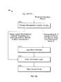
- FIGS. 13a and 13b (sometimes referred to collectively as FIG. 13 ) show an illustrative embodiment of how a read command or request may be handled in distributed flash memory systems in accordance with this disclosure.
- any node (IC 10) may initiate a read command.
- the node initiating such a read command may be referred to as the "requester node” or "the requester.”
- the read command may include the global ID of the requested data block.
- the read command is routed to the node (IC 10) that is the "owner" of the requested data block.
- This routing can take place through the interconnect networks 80/210 of the system.
- the global ID of each data block includes the node ID of that block.
- the node ID identifies the node that is the owner of the block, which enables interconnect networks 80/210 to route the read command to the proper node in the system.
- the owner node checks the status of the data block identified in the read command. Two outcomes of such a check are possible. First, it may be found that the data block is "free” (meaning, e.g., that no node is currently writing to that block). Alternatively, it may be found that the data block is "locked” (meaning, e.g., that some node is currently writing to that block). If the node is free, control passes from 1330 to 1340. We will first continue with this branch from 1330. Later we will come back to the other branch from 1330.
- the circuitry of the owner node reads the requested data out of the block identified in the read command. This will typically require processing the logical block number portion of the global ID of the requested block through the storage manager 1200 ( FIG. 12 ) of the owner node as described earlier in this specification. Also at 1340 the data block thus read out is routed to the requester via the interconnect networks 80/210 of the system. The read data may thus get back to the requester via the same route established for the read request, but in the opposite direction. This satisfies the read request, and so the read protocol can end at 1350.
- the owner node sends a data block non-available status packet back to the requester via the interconnect networks 80/210.
- the requester receives this non-available status packet.
- the requester can try again to satisfy its read request by restarting the protocol at 1310.
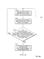
- FIGS. 14a-c show an illustrative embodiment of how a write command or request may be handled in distributed flash memory systems in accordance with the disclosure.
- any node (IC 10) can initiate a write command.
- the node initiating such a write command may be referred to as the "requester node” or "the requester.”
- the write command may include the global ID of the data block into which it is desired to write data.
- Any node (IC 10) in the system may be the "owner” of this data block, where "owner” has the same meaning as used elsewhere in this specification.
- the write command is routed to the owner node. This routing can take place through the interconnect networks 80/210 of the system.
- the global ID of each data block includes the node ID of that block. The node ID identifies the node that is the owner of the block, which enables interconnect networks 80/210 to route the write command to the proper node in the system.
- the owner node checks the status of the data block identified in the write command. If the data block is free (as explained earlier), control passes from 1430 to 1440. If the data block is locked (as also explained earlier), control passes from 1430 to 1460.
- the circuitry of the owner node sends a write acknowledge packet back to the requester via interconnect networks 80/210.
- the requester receives the write acknowledge packet.
- the requester sends the write data packet (i.e., the actual data to be written) to the owner via interconnect networks 80/210.
- the owner writes the write data packet to the data block.
- the write protocol ends.
- the owner sends a data block non-available status packet to the requester via interconnect networks 80/210.
- the requester receives the non-available status packet.
- the requester can retry the write command by starting again at 1410.
- FIGS. 15a-c show an illustrative embodiment of circuitry (or equivalent structure) in accordance with another possible aspect of this disclosure.
- This is structure for providing dynamic data block migration (e.g., within a distributed flash memory system such as is described elsewhere in this specification).
- Each IC 10 in such a system may include an instance of the FIG. 15 structure.
- This structure may be dedicated circuitry on the IC, firmware on the IC, software running on more general-purpose circuitry on the IC, or any combination of the foregoing.
- FIG. 15 shows circuitry (which "circuitry" terminology is again consistent with the generic use of that term herein to refer to circuitry alone or to circuitry with or running software).
- the FIG. 15 circuitry includes one counter 1510 for each data block (e.g., in flash memory 120) connected to the node (IC 10) that includes those counters 1510. Each counter 1510 counts the number of times that this node accesses the associated data block owned by this node.
- the FIG. 15 circuitry also includes M more counters 1512 for each of the N data blocks owned by this node.
- M is the number of other nodes (ICs 10) in the system.
- each of that data block's M counters 1512 is associated with a respective one of the M other nodes in the system.
- Each counter 1512 counts the number of times that the associated other node accesses the associated data block.
- comparator 1514 there is one comparator 1514 associated with each of the counters 1512. (It will be understood that the number of comparators 1514 can be reduced by time-sharing the reduced number of comparators. For example, a single comparator 1514 can be time-shared by all of counters 1512. To simplify the discussion, however, it will be assumed that there is a separate comparator 1514 for each counter 1512.) Each comparator 1514 compares (1) the output 1513 of a respective one of counters 1512, and (2) the output 1511 of the counter 1510 for the same data block that the output 1513 relates to. If (and only if) output 1513 is greater than output 1511, then the comparator 1514 applies an enabling signal to a respective one of comparator circuits 1518. (Output 1511 is the count currently registered by the associated counter 1510. Output 1513 is the count currently registered by the associated counter 1512.)
- comparator 1518 There is one comparator 1518 for each comparator 1514. (Again, the number of comparators 1518 can be reduced by time-sharing as described above in connection with elements 1514.)
- each comparator 1518 compares the output 1513 of a respective one of counters 1512 to a threshold value output by threshold value register 1516. For example, any desired threshold value may be programmed into register 1516. If (and only if) the output 1513 exceeds the threshold value, comparator 1518 produces an output for enabling migration request initiation circuitry 1520.
- circuitry 1520 When circuitry 1520 is enabled as mentioned earlier, circuitry 1520 knows (by knowing which comparator 1518 enabled it) which data block ("the transferred block") needs to be migrated, and to which other node (“the destination node”) that data block needs to be migrated. Circuitry 1520 therefore sends a migration request to the destination node (e.g., via interconnection networks 80/210).
- a migration request (like a read request or a write request) can have the characteristics of a data packet (e.g., as in FIG. 6 and described earlier in this specification).
- a migration request may have a header including the ID of the destination IC, which enables the interconnect resources 80/210 of the system to route the migration request to the destination IC. This is similar to what is done for data packets (e.g., as in FIG. 6 ), read requests, and write requests.
- each node includes all of the elements shown in FIG. 15 . Therefore the illustrated node depicted (in part) in FIG. 15 also includes the elements needed to enable that node to be a destination node.
- the destination node elements can accordingly also be described in connection with FIG. 15 (even though in any actual data block migration two different nodes (i.e., a "source node” originating the migration, and the destination node receiving the migration) will be involved.
- migration request from the source node is received by migration request acceptance circuitry 1530 in the destination node. This circuitry 1530 checks to see whether or not the memory (e.g., 120) connected to that node can receive the data block proposed for transfer (migration).
- Migration request ACK/NAK (acknowledge/non-acknowledge) circuitry 1532 of the destination node sends back to the source node either an ACK signal (meaning that the destination node can receive the data block transfer) or a NAK signal (meaning that the destination node cannot receive the data block transfer).
- migration request ACK/NAK processing circuitry responds to an ACK (and only an ACK) by enabling migration execution circuitry 1542 to actually send the data block to be migrated to the destination node. (A NAK terminates the attempt to migrate the data block.)
- migration report broadcast circuitry 1544 is enabled to send a broadcast message or report notifying all nodes about the migration of the transferred block. For example, the broadcast migration report allows the circuitry 1200 ( FIG. 12 ) in all nodes (ICs 10) in the system to update the records the nodes maintain as to the locations of all data blocks in the system. This is shown in more detail in FIG. 15c , which is discussed in the next paragraph.
- Upper layer system components e.g., file system, database management system, etc., components (not shown)
- FIG. 15b shows elements 1542 and 1544 operating as part of source node operations, they may alternatively operate as part of destination node operations.
- each IC 10 further includes storage management update circuitry 1550 for receiving and processing a migration report that has been broadcast as discussed in connection with element 1544 in FIG. 15b .
- circuitry 1550 causes the logic block manager 1210 in the IC 10 that includes that circuitry 1550 to change in that block manager's records (mapping information) the owner node ID of the transferred block from the source node ID to the destination node ID.
- circuitry 1550 in the source node causes the associated source node flash translation layer 1220 to delete from that translation layer's records (mapping information) the logical block number of the transferred block, while the circuitry 1550 in the destination node causes that circuitry's associated destination node flash translation layer 1220 to add to its records (mapping information) the logical block number of the transferred block.
- Flash device driver 1230 in FIG. 15c has already been fully described in connection with FIG. 12 .
- FIGS. 16a-c (sometimes referred to collectively as FIG. 16 ) show illustrative embodiments of dynamic data block migration methods that can be performed, e.g., by circuitry of the type shown in FIG. 15 in accordance with this disclosure.
- Each node (IC 10) in a distributed memory system may perform the FIG. 16 method.
- each access of each data block by the owner node of that data block is counted.
- each access of each data block by each other node is separately counted.
- each count from 1620 is compared to (1) the count (from 1610) of accesses of the same data block by the node that currently owns that data block, and (2) a threshold value. For any data block whose count (from 1620) for some non-owner node exceeds both the owner node count (from 1610) and the threshold, control passes from 1630 to 1640.
- the last-mentioned data block may be referred to as the transferred block, and the last-mentioned non-owner node may be referred to as the destination node. (If there is no "yes" outcome from 1630, control passes from 1630 back to 1610.)
- the current owner block (“the source block”) sends a request to transfer the transferred block to the destination node.
- the destination node determines whether or not it can accept the proposed transfer. If not, control passes back to 1610 and the proposed transfer does not take place. If the destination block can accept the proposed transfer, control passes to 1660.
- the source node transfers the transferred block to the destination node.
- a message or report is broadcast to all nodes (ICs 10) notifying them about the transfer of the transferred block.
- upper layer elements such as file system elements, database management system elements, etc., are notified about the migration of the transferred block.
- FIG. 16c shows in more detail operations that may be performed in ICs 10 in response to a message broadcast as discussed above in connection with element 1670 in FIG. 16b .
- the FIG. 16c operations are performed to update the records (mapping information) in elements 1210 and 1220 (e.g., FIGS. 12 and 15c ) in view of the data block migration (transfer) that has taken place.
- the record of the owner node ID of the transferred block is changed (from the source node ID to the destination node ID) in all logic block manager circuits 1210 throughout the system.
- the flash translation layer 1220 in the source node has that translation layer's records updated by deleting the logical block number of the transferred block.
- the flash translation layer 1220 in the destination node has that translation layer's records updated by adding the logical block number of the transferred block. (Again, a possible alternative is to perform operations 1674 and 1676 in connection with the actual data migration, rather than in response to a broadcast migration report.)
- references to "data,” “information,” or the like refer to physical embodiments of such data, information, or the like (e.g., as electrical signals, stored electrical charge, particular magnetic states of magnetizable media, etc.). Also throughout this disclosure (as has already been said), terms like “circuit,” “circuitry,” “integrated circuit,” “IC,” and the like can refer to combinations of hardware and software.
- systems can be constructed with any number of nodes (ICs 10) to provide distributed flash memory systems of any desired size.
- ICs nodes
- elements and/or functions that are shown herein as separate may be combined into single elements and/or functions; and elements and/or functions that are shown herein as integral or unitary may be subdivided into two or more separate sub-elements or sub-functions.
Landscapes
- Engineering & Computer Science (AREA)
- Theoretical Computer Science (AREA)
- Physics & Mathematics (AREA)
- General Engineering & Computer Science (AREA)
- General Physics & Mathematics (AREA)
- Techniques For Improving Reliability Of Storages (AREA)
- Memory System Of A Hierarchy Structure (AREA)
Abstract
Description
- This application claims the benefit of
U.S. provisional patent applications No. 61/167,450, filed April 7, 2009 61/169,032, filed April 14, 2009 - Larger data storage has been in increased demand in recent years. Data storage based on solid state flash memory offers compelling advantages in terms of read/write throughput, stability, shock and vibration resistance, etc., compared with traditional magnetic disk based storage. Some such solid state flash memory storage may need to be larger than others, and it can therefore be desirable to be able to use various numbers of identical or substantially identical modules to construct such flash memory storage systems in any of a wide range of sizes. It is also important for such flash storage and the associated memory access circuitry to be able to automatically keep track of where all data is in the memory so that the data can be efficiently and reliably accessed. The present disclosure facilities such aspects of electronic data memory construction and/or operation.
- In accordance with certain possible aspects of the disclosure, a plurality of memory circuits may each be connected to a respective one of a plurality of integrated circuits ("ICs"). Each of the ICs may be connected to at least one other of the ICs by inter-IC connections so that an IC exchanges memory circuit data with another IC via the inter-IC connections. Each of the ICs may include memory manager circuitry that comprises a logic block manager for maintaining a unique global identification ("ID") for each block of data contained in any portion of any of the memory circuits, the global ID including a node ID identifying the IC that is connected to the memory circuit containing that block and a logical block number for that block. The memory manager circuitry for each IC may further comprise a translator for maintaining a mapping between (1) the logical block number of each block contained in the memory circuit connected to the IC that includes that translator, and (2) a physical portion ID of a portion of that memory circuit that contains that block. The memory manager for each IC may still further comprise a driver for receiving the physical portion ID from the translator of the IC that includes that driver and accessing the portion of the memory connected to that IC that is identified by that physical portion ID.
- In accordance with certain other aspects of the disclosure, in memory circuits as summarized above, each of the ICs ("the source IC") may include circuitry for transferring a block ("the transferred block") accessed by the driver of the source IC to another of the ICs ("the destination IC") for storage in the memory circuitry connected to the destination IC.
- In such memory circuits the circuitry for transferring may employ the inter-IC connections.
- In accordance with certain still other possible aspects of the disclosure, in memory circuits as summarized above, each of the ICs ("the source IC") may further include circuitry for maintaining a count of how many times each of the other ICs requests a respective block contained in the memory circuit that is connected to the source IC, and circuitry for the transferring a block ("the transferred block") (for which the count for one of the other ICs ("the destination IC") exceeds a threshold value) from the memory circuit connected to the source IC to the memory circuit connected to the destination IC.
- Still other possible aspects of the disclosure relate to managing access to a plurality of memory circuits, each of which is connected to a respective one of a plurality of integrated circuits ("ICs"). One of the ICs may be connected to at least one of the other ICs by inter-IC connections so that one IC exchanges blocks of memory circuit data with another IC via the inter-IC connections, each of the ICs ("the source IC") including a memory manager. Each such memory manager may comprise circuitry for maintaining a count of how many times a given IC requests at least one block contained in the memory circuit that is connected to the source IC, and circuitry for transferring a block ("the transferred block") (for which the count for one of the other ICs ("the destination IC") exceeds a threshold value) from the memory circuit connected to the source IC to the memory circuit connected to the destination IC.
- In such memory managers the circuitry for transferring may employ the inter-IC connections.
- Further features of the disclosure, its nature and various advantages will be more apparent from the accompanying drawings and the following detailed description.
-
FIG. 1 is a simplified schematic block diagram of an illustrative embodiment of circuitry in accordance with this disclosure. -
FIG. 2 is a simplified logical diagram of an example of a system topology in accordance with the disclosure. -
FIG. 3 is similar toFIG. 2 for another illustrative system topology in accordance with the disclosure. -
FIG. 4 is similar toFIG. 2 for yet another illustrative system topology in accordance with the disclosure. -
FIG. 5 is a more detailed (but still simplified) schematic block diagram of an illustrative embodiment of a portion of theFIG. 1 circuitry in accordance with the disclosure. -
FIG. 6 is a simplified diagram of an illustrative embodiment of a data packet in accordance with the disclosure. -
FIG. 7 is similar toFIG. 5 , but shows an illustrative embodiment of more possible details in accordance with the disclosure. -
FIG. 8 is again similar toFIG. 5 , but shows an illustrative embodiment of still more possible details in accordance with the disclosure. -
FIG. 9 is a simplified schematic block diagram of an illustrative embodiment of a system (or a representative portion of a system) in accordance with the disclosure. -
FIG. 10 is a simplified schematic block diagram of an illustrative embodiment of a portion of theFIG. 1 circuitry in accordance with the disclosure. -
FIG. 11 is a simplified schematic block diagram of an another illustrative embodiment of a portion of theFIG. 1 circuitry in accordance with the disclosure. -
FIG. 12 is a simplified block diagram of an illustrative embodiment of several elements in accordance with certain possible aspects of the disclosure. -
FIGS. 13a and13b (sometimes referred to collectively asFIG. 13 ) are a simplified flow chart of an illustrative embodiment of certain possible method aspects of the disclosure. -
FIGS. 14a-c (sometimes referred to collectively asFIG. 14 ) are a simplified flow chart of an illustrative embodiment of certain other possible method aspects of the disclosure. -
FIGS. 15a-c (sometimes referred to collectively asFIG. 15 ) are a simplified schematic block diagram of an illustrative embodiment of circuitry in accordance with certain possible aspects of the disclosure. -
FIGS. 16a-c (sometimes referred to collectively asFIG. 16 ) are a simplified flow chart of certain, still other possible method aspects of the disclosure. - Illustrative embodiments of electronic data memory systems in which the present disclosure can be implemented and practiced are shown in
Zhou et al. U.S. patent application No. 12/728,757, filed March 22, 2010
FIGS. 1-11 herein are repeated from the Zhou et al. reference and are briefly described below. More detailed description is contained in the text of the Zhou et al. reference. -
FIG. 1 shows an illustrative embodiment of an integrated circuit ("IC") 10 that can be used as part of a distributed electronic data storage or memory system in accordance with this disclosure. (As used herein, terms like "circuit," "circuitry," "integrated circuit," "IC," and the like may refer to circuitry with or without software that runs on the circuitry and/or that controls various operations of the circuitry. As just one illustration of this, an "IC" (as that term is used herein) may include one or more processors with or without software that runs in and/or controls various operations of the processor(s).) The circuitry ofIC 10 includesflash memory controller 20,cache memory controller 30,interface controller 40, direct memory access ("DMA") circuitry 50, central processing unit ("CPU") circuitry 60,bus circuitry 70, andcontrollable routing circuitry 80. IC 10 is connected toflash memory channels 120 andcache memory 130.Flash memory channels 120 are typically the relatively large, main memory forIC 10.Cache memory 130 is typically a smaller, temporary memory forIC 10. For example,cache memory 130 may be used for relatively short-term storage of data on its way to or fromflash memory 120. -
Interface controller 40 can be used for connection ofIC 10 to other circuitry (not shown) that may be thought of as external to the memory system of whichelements IC 10 and the external circuitry. -
Controller 20 controls writing data to and reading data fromflash memory 120.Controller 30 functions similarly forcache memory 130. CPUs 60 provide overall control for IC 10. DMA elements 50 support at least many aspects of memory writing and reading, with less or no involvement of CPUs 60 in such activities.Bus circuitry 70 provides connections between other circuit elements on IC 10.Routing circuitry 80 provides controllable connections (1) betweenbus circuitry 70 andsimilar routing circuitry 80 in one or more other instances ofIC 10, and (2) between such other instances ofIC 10. In a memory system that includes suchmultiple ICs 10, each IC is preferably constructed as shown inFIG. 1 , and each IC is connected to itsown flash memory 120 and itsown buffer memory 130. Accordingly, such a memory system may be referred to as a distributed memory system, and in general such a memory system may include any number ofICs 10, etc., to provide memories having any of a wide range of sizes. -
IC 10 is just one example of how this type of system component can be constructed in accordance with this disclosure. For example, in other embodiments of the disclosure, such an IC may omit some of the elements shown forIC 10 inFIG. 1 , and/or such an IC may have other elements that are not shown forIC 10 inFIG. 1 . -
Routing circuitry 80 may be thought of as a crossbar switch (or at least being like a crossbar switch). In general,such routing circuitry 80 can connect any ofcircuitry 80's ports (labeled P1-P9) to any other ofcircuitry 80's ports (although there may be some inter-port connections that cannot be made).Inter-IC connections 210 are used to connect the "external ports" P4-P9 of depictedIC 10 to similar ports of one or moreother IC 10 instances in the distributed memory system. -
FIGS. 2-4 show some examples of distributed memory system topologies that can be used (although many other topologies are also usable). Eachsmall circle 10 in each ofFIGS. 2-4 represents one instance of anIC 10. Eachline 210 in each ofFIGS. 2-4 represents an inter-IC connection. TheFIG. 2 topology may be referred to as a two-dimensional ("2D") mesh; theFIG. 3 topology may be referred to as a three-dimensional ("3D") mesh; theFIG. 4 topology may be referred to as a triangle cube. -
FIG. 5 shows some additional details as to howrouting circuitry 80 may be constructed. In this construction, each external port P4-P9 is connected to serializer-deserializer ("SERDES") circuitry 512inphysical layer circuitry 510 of routingcircuitry 80. EachSERDES circuitry 512 can convert signals between - (1) serial form on
inter-IC connections 210 and - (2) parallel form for use inside
circuitry 80 and elsewhere onIC 10. (Internal ports P1-P3 may be parallel ports, which do not require SERDES circuitry.) SYNC, align, and ACK/NAK circuitry 522 (inlink layer circuitry 520 of routing circuitry 80) performs synchronization ("SYNC"), alignment ("ALIGN"), and packet acknowledgement ("ACK/NAK") functions for the signals coming from and/or going to each external port P4-P9. Packet routing circuitry 532 (inpacket layer circuitry 530 of routing circuitry 80) performs the actual routing of data packets between selectable different ones of ports P1-P9. - The organization of a typical data packet is shown in
FIG. 6 . For example, such a packet may include a header, which in turn includes anIC 10 identification ("ID") and memory ("MEM") address for the associated actual "data payload". The data payload follows the header, and is in turn followed by cyclic redundancy check ("CRC") or similar information for helping to make sure that the data payload has been correctly received. TheIC 10 ID may also sometimes be referred to as the node ID. -
FIG. 7 shows that some translation may be needed between the information in the header of a packet and the action thatpacket routing circuitry 532 needs to take in order to get a packet from oneIC 10 to anotherIC 10. For example, in a system like that shown inFIG. 2 , it may be necessary to send a packet from the upper right "node" (IC 10) to the lower left "node" (IC 10). This may be due to the data in the packet being stored in theflash memory 120 connected to upperright IC 10, but being needed to satisfy a request for data received byinterface 40 of the lowerleft IC 10. The packet being discussed can be routed from the "source" or "owner" (upper right)IC 10 to the "destination" (lower left)IC 10 via the upper-most arcuateinter-IC connection 210 to the upperleft IC 10, and then via the left-most arcuateinter-IC connection 210 to the lowerleft IC 10. The header for the packet may include the intended destination (IC 10 ID), but thepacket routing circuitry 532 in the upperright IC 10 may need to translate that information into initial information to the effect that a way to get the packet to the lowerleft destination IC 10 is via therouting circuitry 80 of the upperleft IC 10. The routing table circuit 740 (FIG. 7 ) of therouting circuitry 80 of the upperright source IC 10 may therefore be programmed based on the topology of the system (e.g.,FIG. 2 ) to tell the associatedpacket routing circuitry 532 that when thatcircuitry 532 gets a packet that is to be routed to the lowerleft IC 10,circuitry 532 should in fact route that packet to the upperleft IC 10. (The upper left IC will forward that packet on to the lower left destination IC.) -
FIG. 8 shows thatpacket routing circuitry 532 may include input and/oroutput buffer circuitry 850 if needed.Buffer circuitry 850 may be input buffer circuitry and/or output buffer circuitry for buffering data in each of the port channels ofpacket routing circuitry 532. -
FIG. 9 shows an example of a possible physical layout of a distributed flash memory system (or a representative portion of such a system) in accordance with the disclosure.Element 900 is a printed circuit board ("PCB"). SixICs 10a-f are mounted onPCB 900. Also mounted onPCB 900 are theflash memories 120a-f andcache memories 130a-f that are connected to each of ICs 10 (e.g., via circuit traces on PCB 900).Inter-IC connections 210 and external connections 140 (e.g., as inFIG. 1 ) may also be provided (at least in part) as traces onPCB 900. Multiple instances ofPCB 900 may be connected to one another via a backplane on which the PCBs are mounted. -
FIG. 10 shows an illustrative ("crossbar") construction ofrouting circuitry 80. Any two ports P1-P9 can be connected to one another via crossbar conductor(s) CB. The switches S between CB and each of the two ports that it is desired to interconnect are closed (by assertion of appropriate control signals C). All other switches S are open. -
FIG. 11 shows that one crossbar network implementation ofrouting circuitry 80 can concurrently and independently make two or more port-to-port connections. Each such port-to-port connection is made using a respective one of CBa, CBb, etc., and the associated switches Sa, Sb, etc. - The present disclosure provides circuitry and methods (or systems) for providing storage management in a distributed flash storage environment like that illustrated by
FIGS. 1-11 . A storage manager of this disclosure provides memory data block service across distributed storage nodes (e.g., likeICs 10 and their associatedflash 120 andcache 130 memory circuits) to still higher-level structure like a file system or database management system. (A "block" may be any convenient amount of data. For example, a block may be the amount of data that fits in the smallest amount offlash memory 120 that can be separately addressed for data writing or reading. A block will typically be a plurality of data words, but eachflash memory 120 can typically hold many such blocks.) - In accordance with certain possible features of the disclosure, the storage manager may map logical data blocks to physical data blocks of the
flash memories 120. In accordance with certain other possible features of the disclosure, the storage manager may provide dynamic data block migration acrossdifferent storage nodes 10/120/130 to improve data access efficiency. The distributed storage manager is preferably circuitry in and/or software running on each of theICs 10 in the distributed storage system. The storage manager system elements in eachIC 10 are preferably tightly coupled to the storage manager system elements in all of theother ICs 10 in the distributed system. This tight coupling can be via therouting circuitry 80 of the ICs and theinter-IC connections 210 between the ICs. - An illustrative embodiment of a distributed
flash storage manager 1200 is shown inFIG. 12 . As shown in this FIG.,storage manager 1200 has a layered structure.Flash device driver 1230 is the lowest layer in this structure. The next higher layer isflash translation layer 1220. The upper layer is logicblock manager layer 1210. Each of these layers may be circuitry (or may include circuitry) on each instance ofIC 10 in the distributed flash storage system. Alternatively, each of these layers may be or may include corresponding firmware and/or software running in circuitry on each instance ofIC 10 in the distributed system. (Again, as noted earlier in this specification, terms like "circuitry" as used herein are generic to circuitry alone and to circuitry with suitable firmware and/or software.) - Considering first flash
device driver layer 1230, this layer performs hardware-related functions forstorage manager 1200. For example,layer 1230 may provide the actual physical device identification ("ID") for the one of several flash devices 120 (connected to theIC 10 including this particular instance of storage manager 1200) that is to be accessed in a particular memory transaction (data write or data read).Layer 1230 may additionally identify the read/write sector in thatflash device 120 that is to be accessed.Layer 1230 may still further provide the DMA 50 (FIG. 1 ) data transfer (e.g., from flash to cache memory or vice versa). - From the foregoing, it will be seen that the outputs of
layer 1230 are specific to particular physical locations in the immediately associatedmemory elements 120/130 that are to be used in the particular memory transaction being carried out.Layer 1230 gets at least the basics of this physical location information from the associatedflash translation layer 1220. Note, however, thatupper layers layer 1230 only information for blocks that are in thememory elements 120/130 that are connected to theIC 10 that includes this instance ofelements 1200. Thus one of the functions ofupper layers elements 120/130 connected to theIC 10 including thiselement 1200 instance. ("Owned by" means that the block is actually stored in theelements 120/130 that "own" that block.) -
Flash translation layer 1220 typically provides mapping between each "logical" block of memory data and the physical portion (also sometimes referred to as a block) of thememory resources 120/130 that actually contains ("owns") that block of data. A physical block may be identified by a node (IC 10) identification ("ID"), aflash 120 channel number, aflash 120 device number, aflash 120 block number, and aflash 120 sector number. Each logical block may be identified by a node (IC 10) ID and a logical block number.Flash translation layer 1220 may therefore maintain a mapping table whereby each immediately above-mentioned logical block number can be converted to the appropriately corresponding flash channel number, flash device number, flash block number, and flash sector number (all forming parts of a physical portion ID). Again, if (and only if) these last-mentioned physical location numbers are for a block owned by thememory 120 connected to theIC 10 having the associated node ID, then layer 1220 passes these physical location numbers on to the associatedlayer 1230 for use in accessing the identified physical portion of the associatedmemory 120. - Each
layer 1220 may also perform related services like block allocation (e.g., when new data is initially written into memory 120), garbage collection (e.g., when a portion ofmemory 120 no longer contains data that may be needed), and wear leveling (e.g., to avoid excessive over-use of some portions ofmemory 120, while other portions are not being accessed as frequently). -
Logic block manager 1210 provides storage block service to the entire system (i.e., all of thenodes 10/120/130 in an entire system). Each block has a unique global identification ("ID"), which includes a node (IC 10) ID and a logical block number. Any node can request to access any block anywhere in the entire system using the global ID for that block. Based on the node ID portion of the global ID, the request is routed to the correct IC 10 (the "owner" of the requested block). This routing can be performed via therouting circuitry 80 andinter-IC connections 210 needed to get the request from the requesting node to the owner node. When the request reaches the owner node (IC 10), thelogic block manager 1210 applies the logical block number part of the request to theflash translation layer 1220 of thatIC 10. Thatlayer 1220 then processes the logical block number information as described earlier in this specification, leading ultimately to accessing the requested block in theflash memory 120 that is connected to theowner node IC 10. -
FIGS. 13a and13b (sometimes referred to collectively asFIG. 13 ) show an illustrative embodiment of how a read command or request may be handled in distributed flash memory systems in accordance with this disclosure. At 1310, any node (IC 10) may initiate a read command. The node initiating such a read command may be referred to as the "requester node" or "the requester." The read command may include the global ID of the requested data block. - At 1320 the read command is routed to the node (IC 10) that is the "owner" of the requested data block. This routing can take place through the
interconnect networks 80/210 of the system. As noted earlier, the global ID of each data block includes the node ID of that block. The node ID identifies the node that is the owner of the block, which enablesinterconnect networks 80/210 to route the read command to the proper node in the system. - At 1330 the owner node checks the status of the data block identified in the read command. Two outcomes of such a check are possible. First, it may be found that the data block is "free" (meaning, e.g., that no node is currently writing to that block). Alternatively, it may be found that the data block is "locked" (meaning, e.g., that some node is currently writing to that block). If the node is free, control passes from 1330 to 1340. We will first continue with this branch from 1330. Later we will come back to the other branch from 1330.
- At 1340 the circuitry of the owner node reads the requested data out of the block identified in the read command. This will typically require processing the logical block number portion of the global ID of the requested block through the storage manager 1200 (
FIG. 12 ) of the owner node as described earlier in this specification. Also at 1340 the data block thus read out is routed to the requester via theinterconnect networks 80/210 of the system. The read data may thus get back to the requester via the same route established for the read request, but in the opposite direction. This satisfies the read request, and so the read protocol can end at 1350. - Returning now to the other branch from 1330, if the data block is locked, control passes from 1330 to 1360. At 1360, the owner node sends a data block non-available status packet back to the requester via the
interconnect networks 80/210. At 1370 the requester receives this non-available status packet. At 1380 the requester can try again to satisfy its read request by restarting the protocol at 1310. -
FIGS. 14a-c (sometimes referred to collectively asFIG. 14 ) show an illustrative embodiment of how a write command or request may be handled in distributed flash memory systems in accordance with the disclosure. At 1410, any node (IC 10) can initiate a write command. The node initiating such a write command may be referred to as the "requester node" or "the requester." The write command may include the global ID of the data block into which it is desired to write data. Any node (IC 10) in the system may be the "owner" of this data block, where "owner" has the same meaning as used elsewhere in this specification. - At 1420 the write command is routed to the owner node. This routing can take place through the
interconnect networks 80/210 of the system. As noted earlier, the global ID of each data block includes the node ID of that block. The node ID identifies the node that is the owner of the block, which enablesinterconnect networks 80/210 to route the write command to the proper node in the system. - At 1430 the owner node checks the status of the data block identified in the write command. If the data block is free (as explained earlier), control passes from 1430 to 1440. If the data block is locked (as also explained earlier), control passes from 1430 to 1460.
- At 1440 the circuitry of the owner node sends a write acknowledge packet back to the requester via
interconnect networks 80/210. At 1452 the requester receives the write acknowledge packet. At 1454 the requester sends the write data packet (i.e., the actual data to be written) to the owner viainterconnect networks 80/210. At 1456 the owner writes the write data packet to the data block. At 1458 the write protocol ends. - Returning to the other branch from 1430, at 1460 the owner sends a data block non-available status packet to the requester via
interconnect networks 80/210. At 1470 the requester receives the non-available status packet. At 1480 the requester can retry the write command by starting again at 1410. -
FIGS. 15a-c (sometimes collectively referred to asFIG. 15 ) show an illustrative embodiment of circuitry (or equivalent structure) in accordance with another possible aspect of this disclosure. This is structure for providing dynamic data block migration (e.g., within a distributed flash memory system such as is described elsewhere in this specification). EachIC 10 in such a system may include an instance of theFIG. 15 structure. This structure may be dedicated circuitry on the IC, firmware on the IC, software running on more general-purpose circuitry on the IC, or any combination of the foregoing. To simplify the following discussion, it will be assumed thatFIG. 15 shows circuitry (which "circuitry" terminology is again consistent with the generic use of that term herein to refer to circuitry alone or to circuitry with or running software). - The
FIG. 15 circuitry includes onecounter 1510 for each data block (e.g., in flash memory 120) connected to the node (IC 10) that includes thosecounters 1510. Eachcounter 1510 counts the number of times that this node accesses the associated data block owned by this node. - The
FIG. 15 circuitry also includes Mmore counters 1512 for each of the N data blocks owned by this node. M is the number of other nodes (ICs 10) in the system. For each data block, each of that data block's M counters 1512 is associated with a respective one of the M other nodes in the system. Eachcounter 1512 counts the number of times that the associated other node accesses the associated data block. - There is one
comparator 1514 associated with each of thecounters 1512. (It will be understood that the number ofcomparators 1514 can be reduced by time-sharing the reduced number of comparators. For example, asingle comparator 1514 can be time-shared by all ofcounters 1512. To simplify the discussion, however, it will be assumed that there is aseparate comparator 1514 for eachcounter 1512.) Eachcomparator 1514 compares (1) theoutput 1513 of a respective one ofcounters 1512, and (2) theoutput 1511 of thecounter 1510 for the same data block that theoutput 1513 relates to. If (and only if)output 1513 is greater thanoutput 1511, then thecomparator 1514 applies an enabling signal to a respective one ofcomparator circuits 1518. (Output 1511 is the count currently registered by the associatedcounter 1510.Output 1513 is the count currently registered by the associatedcounter 1512.) - There is one
comparator 1518 for eachcomparator 1514. (Again, the number ofcomparators 1518 can be reduced by time-sharing as described above in connection withelements 1514.) - When enabled, each
comparator 1518 compares theoutput 1513 of a respective one ofcounters 1512 to a threshold value output bythreshold value register 1516. For example, any desired threshold value may be programmed intoregister 1516. If (and only if) theoutput 1513 exceeds the threshold value,comparator 1518 produces an output for enabling migrationrequest initiation circuitry 1520. - The significance of the foregoing is as follows. Whenever the count of accesses of a data block by a non-owner node exceeds both (1) the number of accesses of the data block by that data block's current owner node and (2) a predetermined threshold number of accesses (from register 1516), an attempt will be made to migrate (transfer) that data block from the current owner node to the above-mentioned other node in order to make that other node the new owner of the data block. This tends to give ownership of each data block to the node that is making most frequent use of (i.e., most frequently accessing) that data block. This can greatly increase the access efficiency of the distributed memory system as a whole. The data block migrations needed to produce this result are carried out by
elements FIG. 15b , as will now be described. - When
circuitry 1520 is enabled as mentioned earlier,circuitry 1520 knows (by knowing whichcomparator 1518 enabled it) which data block ("the transferred block") needs to be migrated, and to which other node ("the destination node") that data block needs to be migrated.Circuitry 1520 therefore sends a migration request to the destination node (e.g., viainterconnection networks 80/210). A migration request (like a read request or a write request) can have the characteristics of a data packet (e.g., as inFIG. 6 and described earlier in this specification). Thus, for example, a migration request may have a header including the ID of the destination IC, which enables theinterconnect resources 80/210 of the system to route the migration request to the destination IC. This is similar to what is done for data packets (e.g., as inFIG. 6 ), read requests, and write requests. - As mentioned earlier, each node (IC 10) includes all of the elements shown in
FIG. 15 . Therefore the illustrated node depicted (in part) inFIG. 15 also includes the elements needed to enable that node to be a destination node. The destination node elements can accordingly also be described in connection withFIG. 15 (even though in any actual data block migration two different nodes (i.e., a "source node" originating the migration, and the destination node receiving the migration) will be involved. Thus the migration request from the source node is received by migrationrequest acceptance circuitry 1530 in the destination node. Thiscircuitry 1530 checks to see whether or not the memory (e.g., 120) connected to that node can receive the data block proposed for transfer (migration). Migration request ACK/NAK (acknowledge/non-acknowledge)circuitry 1532 of the destination node sends back to the source node either an ACK signal (meaning that the destination node can receive the data block transfer) or a NAK signal (meaning that the destination node cannot receive the data block transfer). - In the source node, migration request ACK/NAK processing circuitry responds to an ACK (and only an ACK) by enabling
migration execution circuitry 1542 to actually send the data block to be migrated to the destination node. (A NAK terminates the attempt to migrate the data block.) When the data block migration has been successfully accomplished, migrationreport broadcast circuitry 1544 is enabled to send a broadcast message or report notifying all nodes about the migration of the transferred block. For example, the broadcast migration report allows the circuitry 1200 (FIG. 12 ) in all nodes (ICs 10) in the system to update the records the nodes maintain as to the locations of all data blocks in the system. This is shown in more detail inFIG. 15c , which is discussed in the next paragraph. Upper layer system components (e.g., file system, database management system, etc., components (not shown)) may also be notified about the migration of the block (e.g., via an external link 140 (FIG. 1 )). AlthoughFIG. 15b showselements - As shown in
FIG. 15c , eachIC 10 further includes storagemanagement update circuitry 1550 for receiving and processing a migration report that has been broadcast as discussed in connection withelement 1544 inFIG. 15b . When such a migration report is received,circuitry 1550 causes thelogic block manager 1210 in theIC 10 that includes thatcircuitry 1550 to change in that block manager's records (mapping information) the owner node ID of the transferred block from the source node ID to the destination node ID. Similarly,circuitry 1550 in the source node causes the associated source nodeflash translation layer 1220 to delete from that translation layer's records (mapping information) the logical block number of the transferred block, while thecircuitry 1550 in the destination node causes that circuitry's associated destination nodeflash translation layer 1220 to add to its records (mapping information) the logical block number of the transferred block. (As an alternative to making these changes to thetranslation layer 1220 records in response to the broadcast migration report, these changes could instead be made as part of the data migration operation itself, because these changes only affect the translation layers in the source and destination nodes involved in the migration.)Flash device driver 1230 inFIG. 15c has already been fully described in connection withFIG. 12 . -
FIGS. 16a-c (sometimes referred to collectively asFIG. 16 ) show illustrative embodiments of dynamic data block migration methods that can be performed, e.g., by circuitry of the type shown inFIG. 15 in accordance with this disclosure. Each node (IC 10) in a distributed memory system may perform theFIG. 16 method. - At 1610 each access of each data block by the owner node of that data block is counted.
- At 1620 each access of each data block by each other node is separately counted.
- At 1630 each count from 1620 is compared to (1) the count (from 1610) of accesses of the same data block by the node that currently owns that data block, and (2) a threshold value. For any data block whose count (from 1620) for some non-owner node exceeds both the owner node count (from 1610) and the threshold, control passes from 1630 to 1640. The last-mentioned data block may be referred to as the transferred block, and the last-mentioned non-owner node may be referred to as the destination node. (If there is no "yes" outcome from 1630, control passes from 1630 back to 1610.)
- At 1640 the current owner block ("the source block") sends a request to transfer the transferred block to the destination node.
- At 1650 the destination node determines whether or not it can accept the proposed transfer. If not, control passes back to 1610 and the proposed transfer does not take place. If the destination block can accept the proposed transfer, control passes to 1660.
- At 1660 the source node transfers the transferred block to the destination node. At 1670 a message or report is broadcast to all nodes (ICs 10) notifying them about the transfer of the transferred block. At 1680 upper layer elements such as file system elements, database management system elements, etc., are notified about the migration of the transferred block.
-
FIG. 16c shows in more detail operations that may be performed inICs 10 in response to a message broadcast as discussed above in connection withelement 1670 inFIG. 16b . TheFIG. 16c operations are performed to update the records (mapping information) inelements 1210 and 1220 (e.g.,FIGS. 12 and15c ) in view of the data block migration (transfer) that has taken place. At 1672 the record of the owner node ID of the transferred block is changed (from the source node ID to the destination node ID) in all logicblock manager circuits 1210 throughout the system. At 1674 theflash translation layer 1220 in the source node has that translation layer's records updated by deleting the logical block number of the transferred block. At 1676 theflash translation layer 1220 in the destination node has that translation layer's records updated by adding the logical block number of the transferred block. (Again, a possible alternative is to performoperations - Throughout this disclosure, references to "data," "information," or the like refer to physical embodiments of such data, information, or the like (e.g., as electrical signals, stored electrical charge, particular magnetic states of magnetizable media, etc.). Also throughout this disclosure (as has already been said), terms like "circuit," "circuitry," "integrated circuit," "IC," and the like can refer to combinations of hardware and software.
- It will be understood that the foregoing is only illustrative of the principles of the disclosure, and that various modifications can be made by those skilled in the art without departing from the scope and spirit of the disclosure. For example, systems can be constructed with any number of nodes (ICs 10) to provide distributed flash memory systems of any desired size. As another example of modifications within the scope of this disclosure, elements and/or functions that are shown herein as separate may be combined into single elements and/or functions; and elements and/or functions that are shown herein as integral or unitary may be subdivided into two or more separate sub-elements or sub-functions.
Claims (20)
- A plurality of memory circuits, each of which is connected to a respective one of a plurality of integrated circuits ("ICs"), each of the ICs being connected to at least one of the other ICs by inter-IC connections so that an IC exchanges memory circuit data with another IC via the inter-IC connections, each of the ICs including memory manager circuitry comprising:a logic block manager for maintaining a unique global identification ("ID") for each block of data contained in any portion of any of the memory circuits, the global ID including a node ID identifying the IC that is connected to the memory circuit containing that block and a logical block number for that block;a translator for maintaining a mapping between (1) the logical block number of each block contained in the memory circuit connected to the IC that includes that translator, and (2) a physical portion ID of a portion of that memory circuit that contains that block; anda driver for receiving the physical portion ID from the translator of the IC that includes that driver and accessing the portion of the memory connected to that IC that is identified by that physical portion ID.
- The memory circuits defined in claim 1 wherein at least one of ICs includes circuitry for receiving a request from an external source for a block identified by the global ID of that requested block, and wherein the logic block manager of that IC includes circuitry for using the global ID of the requested block to determine the node ID and the logical block number of the requested block.
- The memory circuits defined in claim 2 wherein if the circuitry for using determines that the node ID of the requested block is the node ID of the IC that includes that circuitry for using, then the logic block manager circuitry of that IC applies the logical block number of the requested block to the translator of that IC.
- The memory circuits defined in claim 2 wherein if the circuitry for using determines that the node ID of the requested block is not the node ID of the IC that includes that circuitry for using, then the logic block manager circuitry of that IC employs circuitry for causing that IC to route data for the request to at least one other of the ICs.
- The memory circuits defined in claim 4 wherein the circuitry for causing uses at least one of the inter-IC connections to route data for the request to at least one other of the ICs.
- The memory circuits defined in claim 4 wherein the circuitry for causing is responsive to node ID data in the request to select a route for the request to at least one other of the ICs.
- The memory circuits defined in claim 6 wherein the circuitry for causing is additionally responsive to data, stored in the IC that includes that circuitry for causing, indicative of topology of the ICs and the inter-IC connections.
- The memory circuits defined in claim 4 wherein, when the request reaches the other IC ("the reading IC") having the node ID of the requested block, the logic block manager of the reading IC applies the logic block number of the requested block to the translator of the reading IC.
- The memory circuits defined in claim 8 wherein the driver of the reading IC reads the requested data from the memory circuitry connected to the reading IC so that the reading IC routes that data back to the IC that received the request from the external source.
- The memory circuits defined in claim 1 wherein each of the ICs ("the source IC") includes circuitry for transferring a block ("the transferred block") accessed by the driver of the source IC to another of the ICs ("the destination IC") for storage in the memory circuitry connected to the destination IC.
- The memory circuits defined in claim 10 wherein the circuitry for transferring employs the inter-IC connections.
- The memory circuits defined in claim 10 further comprising:circuitry for updating the mapping of the translator of the source IC to delete the logical block number of the transferred block, and for updating the mapping of the translator of the destination IC to add the logical block number of the transferred block.
- The memory circuits defined in claim 10 further comprising:circuitry for changing the node ID of the transferred block in the block manager in all of the ICs from the node ID of the source IC to the node ID of the destination IC.
- The memory circuits defined in claim 1 wherein each of the ICs ("the source IC") further includes:circuitry for maintaining a count of how many times each of the other ICs requests a respective block contained in the memory circuit that is connected to the source IC; andcircuitry for transferring a block ("the transferred block"), for which the count for one of the other ICs ("the destination IC") exceeds a threshold value, from the memory circuit connected to the source IC to the memory circuit connected to the destination IC.
- The memory circuits defined in claim 14 wherein the circuitry for transferring employs the inter-IC connections.
- The memory circuits defined in claim 14 further comprising:circuitry for updating the mapping of the translator of the source IC to delete the logical block number of the transferred block, and for updating the mapping of the translaor of the destination IC to add the logical block number of the transferred block.
- The memory circuits defined in claim 14 further comprising:circuitry for changing the node ID of the transferred block in the block manager in at least one of the ICs from the node ID of the source IC to the node ID of the destination IC.
- Managing access to a plurality of memory circuits, each of which is connected to a respective one of a plurality of integrated circuits ("ICs"), one of the ICs being connected to at least one of the other ICs by inter-IC connections so that one IC exchanges blocks of memory circuit data with another IC via the inter-IC connections, each of the ICs ("the source IC") including a memory manager comprising:circuitry for maintaining a count of how many times a given IC requests at least one block contained in the memory circuit that is connected to the source IC; andcircuitry for transferring a block ("the transferred block"), for which the count for one of the other ICs ("the destination IC") exceeds a threshold value, from the memory circuit connected to the source IC to the memory circuit connected to the destination IC.
- The memory manager defined in claim 18 wherein the circuitry for transferring employs the inter-IC connections.
- The memory manager defined in claim 18 wherein an IC further comprises:circuitry for maintaining a record of where a given block is currently stored, said record including a node identification ("ID") which identifies the IC that is connected to the memory circuit in which a given block is currently stored.
Applications Claiming Priority (2)
| Application Number | Priority Date | Filing Date | Title |
|---|---|---|---|
| US16745009P | 2009-04-07 | 2009-04-07 | |
| US16903209P | 2009-04-14 | 2009-04-14 |
Publications (2)
| Publication Number | Publication Date |
|---|---|
| EP2239665A1 true EP2239665A1 (en) | 2010-10-13 |
| EP2239665B1 EP2239665B1 (en) | 2016-07-13 |
Family
ID=42325468
Family Applications (1)
| Application Number | Title | Priority Date | Filing Date |
|---|---|---|---|
| EP10159218.6A Not-in-force EP2239665B1 (en) | 2009-04-07 | 2010-04-07 | Distributed flash memory storage manager systems |
Country Status (2)
| Country | Link |
|---|---|
| US (2) | US8270194B2 (en) |
| EP (1) | EP2239665B1 (en) |
Families Citing this family (5)
| Publication number | Priority date | Publication date | Assignee | Title |
|---|---|---|---|---|
| KR101473344B1 (en) * | 2007-08-24 | 2014-12-17 | 삼성전자 주식회사 | Devices that use flash memory as storage and how they work |
| US8270194B2 (en) * | 2009-04-07 | 2012-09-18 | Marvell World Trade Ltd. | Distributed flash memory storage manager systems |
| US9135191B1 (en) * | 2012-06-15 | 2015-09-15 | Symantec Corporation | Techniques for storage network bandwidth management |
| KR101512296B1 (en) * | 2013-04-05 | 2015-04-15 | 주식회사 팬택 | File associated with application processing terminal and processing method of file associated with application |
| CN107908364B (en) * | 2017-11-13 | 2020-10-23 | 中国电子科技集团公司第三十研究所 | Embedded file system based on norflash |
Citations (3)
| Publication number | Priority date | Publication date | Assignee | Title |
|---|---|---|---|---|
| US5822785A (en) * | 1992-12-18 | 1998-10-13 | Fujitsu Limited | Data transfer using local and global address translation and authorization |
| US20070220195A1 (en) * | 2006-03-20 | 2007-09-20 | Nec Corporation | Multi-processor system, and method of distributing memory access load in multi-processor system |
| US20090240869A1 (en) * | 2008-03-20 | 2009-09-24 | Schooner Information Technology, Inc. | Sharing Data Fabric for Coherent-Distributed Caching of Multi-Node Shared-Distributed Flash Memory |
Family Cites Families (3)
| Publication number | Priority date | Publication date | Assignee | Title |
|---|---|---|---|---|
| JP2625385B2 (en) * | 1994-06-30 | 1997-07-02 | 日本電気株式会社 | Multiprocessor system |
| US5897664A (en) * | 1996-07-01 | 1999-04-27 | Sun Microsystems, Inc. | Multiprocessor system having mapping table in each node to map global physical addresses to local physical addresses of page copies |
| US8270194B2 (en) * | 2009-04-07 | 2012-09-18 | Marvell World Trade Ltd. | Distributed flash memory storage manager systems |
-
2010
- 2010-04-05 US US12/754,376 patent/US8270194B2/en active Active
- 2010-04-07 EP EP10159218.6A patent/EP2239665B1/en not_active Not-in-force
-
2012
- 2012-09-05 US US13/603,994 patent/US8422264B2/en active Active
Patent Citations (3)
| Publication number | Priority date | Publication date | Assignee | Title |
|---|---|---|---|---|
| US5822785A (en) * | 1992-12-18 | 1998-10-13 | Fujitsu Limited | Data transfer using local and global address translation and authorization |
| US20070220195A1 (en) * | 2006-03-20 | 2007-09-20 | Nec Corporation | Multi-processor system, and method of distributing memory access load in multi-processor system |
| US20090240869A1 (en) * | 2008-03-20 | 2009-09-24 | Schooner Information Technology, Inc. | Sharing Data Fabric for Coherent-Distributed Caching of Multi-Node Shared-Distributed Flash Memory |
Also Published As
| Publication number | Publication date |
|---|---|
| EP2239665B1 (en) | 2016-07-13 |
| US20100254173A1 (en) | 2010-10-07 |
| US20120327697A1 (en) | 2012-12-27 |
| US8422264B2 (en) | 2013-04-16 |
| US8270194B2 (en) | 2012-09-18 |
Similar Documents
| Publication | Publication Date | Title |
|---|---|---|
| US12132581B2 (en) | Network interface controller with eviction cache | |
| US10389839B2 (en) | Method and apparatus for generating data prefetches specifying various sizes to prefetch data from a remote computing node | |
| US6751703B2 (en) | Data storage systems and methods which utilize an on-board cache | |
| CN103080917B (en) | expandable storage device | |
| US8572206B2 (en) | Transaction processing using multiple protocol engines | |
| JP5931816B2 (en) | Storage device | |
| CN104508644B (en) | Intelligence memory buffer | |
| US20110145452A1 (en) | Methods and apparatus for distribution of raid storage management over a sas domain | |
| JP2020021495A (en) | Hybrid memory cube system interconnect directory-based cache coherence methodology | |
| WO2011151859A1 (en) | Data transfer device and method of controlling the same | |
| US20160253123A1 (en) | NVMM: An Extremely Large, Logically Unified, Sequentially Consistent Main-Memory System | |
| EP2075983A2 (en) | Storage subsystem | |
| US20240338330A1 (en) | Apparatus and method for supporting data input/output operation based on a data attribute in a shared memory device or a memory expander | |
| CN106462524A (en) | Interconnect system and method using hybrid memory cube links | |
| US8422264B2 (en) | Distributed flash memory storage manager systems | |
| CN114238156B (en) | Processing system and method of operating a processing system | |
| CN115550293B (en) | FSI main controller and port routing device and method thereof | |
| CN119166566A (en) | Storage controller and electronic system | |
| US9164914B1 (en) | Multiple port routing circuitry for flash memory storage systems | |
| CN1318991C (en) | Data transfer unit with support for multiple coherency granules | |
| JP4774099B2 (en) | Arithmetic processing apparatus, information processing apparatus, and control method for arithmetic processing apparatus | |
| JP2015041290A (en) | Storage device | |
| KR20250053716A (en) | Method and architecture for accelerating comutational storage in all-flash-array network | |
| CN110209343A (en) | Date storage method, device, server and storage medium | |
| WO2025128115A1 (en) | Address space support for point-to-point cache coherency |
Legal Events
| Date | Code | Title | Description |
|---|---|---|---|
| PUAI | Public reference made under article 153(3) epc to a published international application that has entered the european phase |
Free format text: ORIGINAL CODE: 0009012 |
|
| AK | Designated contracting states |
Kind code of ref document: A1 Designated state(s): AT BE BG CH CY CZ DE DK EE ES FI FR GB GR HR HU IE IS IT LI LT LU LV MC MK MT NL NO PL PT RO SE SI SK SM TR |
|
| AX | Request for extension of the european patent |
Extension state: AL BA ME RS |
|
| 17P | Request for examination filed |
Effective date: 20110413 |
|
| 17Q | First examination report despatched |
Effective date: 20121122 |
|
| GRAP | Despatch of communication of intention to grant a patent |
Free format text: ORIGINAL CODE: EPIDOSNIGR1 |
|
| INTG | Intention to grant announced |
Effective date: 20160215 |
|
| GRAS | Grant fee paid |
Free format text: ORIGINAL CODE: EPIDOSNIGR3 |
|
| GRAA | (expected) grant |
Free format text: ORIGINAL CODE: 0009210 |
|
| AK | Designated contracting states |
Kind code of ref document: B1 Designated state(s): AT BE BG CH CY CZ DE DK EE ES FI FR GB GR HR HU IE IS IT LI LT LU LV MC MK MT NL NO PL PT RO SE SI SK SM TR |
|
| REG | Reference to a national code |
Ref country code: GB Ref legal event code: FG4D |
|
| REG | Reference to a national code |
Ref country code: AT Ref legal event code: REF Ref document number: 812811 Country of ref document: AT Kind code of ref document: T Effective date: 20160715 Ref country code: CH Ref legal event code: EP |
|
| REG | Reference to a national code |
Ref country code: IE Ref legal event code: FG4D |
|
| REG | Reference to a national code |
Ref country code: DE Ref legal event code: R096 Ref document number: 602010034610 Country of ref document: DE |
|
| REG | Reference to a national code |
Ref country code: LT Ref legal event code: MG4D |
|
| REG | Reference to a national code |
Ref country code: NL Ref legal event code: MP Effective date: 20160713 |
|
| REG | Reference to a national code |
Ref country code: AT Ref legal event code: MK05 Ref document number: 812811 Country of ref document: AT Kind code of ref document: T Effective date: 20160713 |
|
| PG25 | Lapsed in a contracting state [announced via postgrant information from national office to epo] |
Ref country code: LT Free format text: LAPSE BECAUSE OF FAILURE TO SUBMIT A TRANSLATION OF THE DESCRIPTION OR TO PAY THE FEE WITHIN THE PRESCRIBED TIME-LIMIT Effective date: 20160713 Ref country code: HR Free format text: LAPSE BECAUSE OF FAILURE TO SUBMIT A TRANSLATION OF THE DESCRIPTION OR TO PAY THE FEE WITHIN THE PRESCRIBED TIME-LIMIT Effective date: 20160713 Ref country code: IT Free format text: LAPSE BECAUSE OF FAILURE TO SUBMIT A TRANSLATION OF THE DESCRIPTION OR TO PAY THE FEE WITHIN THE PRESCRIBED TIME-LIMIT Effective date: 20160713 Ref country code: NL Free format text: LAPSE BECAUSE OF FAILURE TO SUBMIT A TRANSLATION OF THE DESCRIPTION OR TO PAY THE FEE WITHIN THE PRESCRIBED TIME-LIMIT Effective date: 20160713 Ref country code: NO Free format text: LAPSE BECAUSE OF FAILURE TO SUBMIT A TRANSLATION OF THE DESCRIPTION OR TO PAY THE FEE WITHIN THE PRESCRIBED TIME-LIMIT Effective date: 20161013 Ref country code: FI Free format text: LAPSE BECAUSE OF FAILURE TO SUBMIT A TRANSLATION OF THE DESCRIPTION OR TO PAY THE FEE WITHIN THE PRESCRIBED TIME-LIMIT Effective date: 20160713 Ref country code: IS Free format text: LAPSE BECAUSE OF FAILURE TO SUBMIT A TRANSLATION OF THE DESCRIPTION OR TO PAY THE FEE WITHIN THE PRESCRIBED TIME-LIMIT Effective date: 20161113 |
|
| PG25 | Lapsed in a contracting state [announced via postgrant information from national office to epo] |
Ref country code: SE Free format text: LAPSE BECAUSE OF FAILURE TO SUBMIT A TRANSLATION OF THE DESCRIPTION OR TO PAY THE FEE WITHIN THE PRESCRIBED TIME-LIMIT Effective date: 20160713 Ref country code: PT Free format text: LAPSE BECAUSE OF FAILURE TO SUBMIT A TRANSLATION OF THE DESCRIPTION OR TO PAY THE FEE WITHIN THE PRESCRIBED TIME-LIMIT Effective date: 20161114 Ref country code: ES Free format text: LAPSE BECAUSE OF FAILURE TO SUBMIT A TRANSLATION OF THE DESCRIPTION OR TO PAY THE FEE WITHIN THE PRESCRIBED TIME-LIMIT Effective date: 20160713 Ref country code: LV Free format text: LAPSE BECAUSE OF FAILURE TO SUBMIT A TRANSLATION OF THE DESCRIPTION OR TO PAY THE FEE WITHIN THE PRESCRIBED TIME-LIMIT Effective date: 20160713 Ref country code: BE Free format text: LAPSE BECAUSE OF FAILURE TO SUBMIT A TRANSLATION OF THE DESCRIPTION OR TO PAY THE FEE WITHIN THE PRESCRIBED TIME-LIMIT Effective date: 20160713 Ref country code: GR Free format text: LAPSE BECAUSE OF FAILURE TO SUBMIT A TRANSLATION OF THE DESCRIPTION OR TO PAY THE FEE WITHIN THE PRESCRIBED TIME-LIMIT Effective date: 20161014 Ref country code: AT Free format text: LAPSE BECAUSE OF FAILURE TO SUBMIT A TRANSLATION OF THE DESCRIPTION OR TO PAY THE FEE WITHIN THE PRESCRIBED TIME-LIMIT Effective date: 20160713 Ref country code: PL Free format text: LAPSE BECAUSE OF FAILURE TO SUBMIT A TRANSLATION OF THE DESCRIPTION OR TO PAY THE FEE WITHIN THE PRESCRIBED TIME-LIMIT Effective date: 20160713 |
|
| REG | Reference to a national code |
Ref country code: DE Ref legal event code: R097 Ref document number: 602010034610 Country of ref document: DE |
|
| REG | Reference to a national code |
Ref country code: FR Ref legal event code: PLFP Year of fee payment: 8 |
|
| PG25 | Lapsed in a contracting state [announced via postgrant information from national office to epo] |
Ref country code: EE Free format text: LAPSE BECAUSE OF FAILURE TO SUBMIT A TRANSLATION OF THE DESCRIPTION OR TO PAY THE FEE WITHIN THE PRESCRIBED TIME-LIMIT Effective date: 20160713 Ref country code: RO Free format text: LAPSE BECAUSE OF FAILURE TO SUBMIT A TRANSLATION OF THE DESCRIPTION OR TO PAY THE FEE WITHIN THE PRESCRIBED TIME-LIMIT Effective date: 20160713 |
|
| PLBE | No opposition filed within time limit |
Free format text: ORIGINAL CODE: 0009261 |
|
| STAA | Information on the status of an ep patent application or granted ep patent |
Free format text: STATUS: NO OPPOSITION FILED WITHIN TIME LIMIT |
|
| PG25 | Lapsed in a contracting state [announced via postgrant information from national office to epo] |
Ref country code: DK Free format text: LAPSE BECAUSE OF FAILURE TO SUBMIT A TRANSLATION OF THE DESCRIPTION OR TO PAY THE FEE WITHIN THE PRESCRIBED TIME-LIMIT Effective date: 20160713 Ref country code: CZ Free format text: LAPSE BECAUSE OF FAILURE TO SUBMIT A TRANSLATION OF THE DESCRIPTION OR TO PAY THE FEE WITHIN THE PRESCRIBED TIME-LIMIT Effective date: 20160713 Ref country code: SM Free format text: LAPSE BECAUSE OF FAILURE TO SUBMIT A TRANSLATION OF THE DESCRIPTION OR TO PAY THE FEE WITHIN THE PRESCRIBED TIME-LIMIT Effective date: 20160713 Ref country code: SK Free format text: LAPSE BECAUSE OF FAILURE TO SUBMIT A TRANSLATION OF THE DESCRIPTION OR TO PAY THE FEE WITHIN THE PRESCRIBED TIME-LIMIT Effective date: 20160713 Ref country code: BG Free format text: LAPSE BECAUSE OF FAILURE TO SUBMIT A TRANSLATION OF THE DESCRIPTION OR TO PAY THE FEE WITHIN THE PRESCRIBED TIME-LIMIT Effective date: 20161013 |
|
| 26N | No opposition filed |
Effective date: 20170418 |
|
| PG25 | Lapsed in a contracting state [announced via postgrant information from national office to epo] |
Ref country code: SI Free format text: LAPSE BECAUSE OF FAILURE TO SUBMIT A TRANSLATION OF THE DESCRIPTION OR TO PAY THE FEE WITHIN THE PRESCRIBED TIME-LIMIT Effective date: 20160713 |
|
| REG | Reference to a national code |
Ref country code: CH Ref legal event code: PL |
|
| REG | Reference to a national code |
Ref country code: IE Ref legal event code: MM4A |
|
| PG25 | Lapsed in a contracting state [announced via postgrant information from national office to epo] |
Ref country code: MC Free format text: LAPSE BECAUSE OF FAILURE TO SUBMIT A TRANSLATION OF THE DESCRIPTION OR TO PAY THE FEE WITHIN THE PRESCRIBED TIME-LIMIT Effective date: 20160713 |
|
| PG25 | Lapsed in a contracting state [announced via postgrant information from national office to epo] |
Ref country code: LI Free format text: LAPSE BECAUSE OF NON-PAYMENT OF DUE FEES Effective date: 20170430 Ref country code: CH Free format text: LAPSE BECAUSE OF NON-PAYMENT OF DUE FEES Effective date: 20170430 Ref country code: LU Free format text: LAPSE BECAUSE OF NON-PAYMENT OF DUE FEES Effective date: 20170407 |
|
| REG | Reference to a national code |
Ref country code: FR Ref legal event code: PLFP Year of fee payment: 9 |
|
| PG25 | Lapsed in a contracting state [announced via postgrant information from national office to epo] |
Ref country code: IE Free format text: LAPSE BECAUSE OF NON-PAYMENT OF DUE FEES Effective date: 20170407 |
|
| PG25 | Lapsed in a contracting state [announced via postgrant information from national office to epo] |
Ref country code: MT Free format text: LAPSE BECAUSE OF NON-PAYMENT OF DUE FEES Effective date: 20170407 |
|
| PG25 | Lapsed in a contracting state [announced via postgrant information from national office to epo] |
Ref country code: HU Free format text: LAPSE BECAUSE OF FAILURE TO SUBMIT A TRANSLATION OF THE DESCRIPTION OR TO PAY THE FEE WITHIN THE PRESCRIBED TIME-LIMIT; INVALID AB INITIO Effective date: 20100407 |
|
| PGFP | Annual fee paid to national office [announced via postgrant information from national office to epo] |
Ref country code: DE Payment date: 20190621 Year of fee payment: 10 |
|
| PGFP | Annual fee paid to national office [announced via postgrant information from national office to epo] |
Ref country code: FR Payment date: 20190424 Year of fee payment: 10 |
|
| PG25 | Lapsed in a contracting state [announced via postgrant information from national office to epo] |
Ref country code: CY Free format text: LAPSE BECAUSE OF NON-PAYMENT OF DUE FEES Effective date: 20160713 |
|
| PGFP | Annual fee paid to national office [announced via postgrant information from national office to epo] |
Ref country code: GB Payment date: 20190429 Year of fee payment: 10 |
|
| PG25 | Lapsed in a contracting state [announced via postgrant information from national office to epo] |
Ref country code: MK Free format text: LAPSE BECAUSE OF FAILURE TO SUBMIT A TRANSLATION OF THE DESCRIPTION OR TO PAY THE FEE WITHIN THE PRESCRIBED TIME-LIMIT Effective date: 20160713 |
|
| PG25 | Lapsed in a contracting state [announced via postgrant information from national office to epo] |
Ref country code: TR Free format text: LAPSE BECAUSE OF FAILURE TO SUBMIT A TRANSLATION OF THE DESCRIPTION OR TO PAY THE FEE WITHIN THE PRESCRIBED TIME-LIMIT Effective date: 20160713 |
|
| REG | Reference to a national code |
Ref country code: DE Ref legal event code: R082 Ref document number: 602010034610 Country of ref document: DE Representative=s name: GRUENECKER PATENT- UND RECHTSANWAELTE PARTG MB, DE Ref country code: DE Ref legal event code: R081 Ref document number: 602010034610 Country of ref document: DE Owner name: MARVELL ASIA PTE, LTD., SG Free format text: FORMER OWNER: MARVELL WORLD TRADE LTD., ST. MICHAEL, BB |
|
| REG | Reference to a national code |
Ref country code: GB Ref legal event code: 732E Free format text: REGISTERED BETWEEN 20200709 AND 20200715 |
|
| REG | Reference to a national code |
Ref country code: DE Ref legal event code: R119 Ref document number: 602010034610 Country of ref document: DE |
|
| PG25 | Lapsed in a contracting state [announced via postgrant information from national office to epo] |
Ref country code: DE Free format text: LAPSE BECAUSE OF NON-PAYMENT OF DUE FEES Effective date: 20201103 Ref country code: FR Free format text: LAPSE BECAUSE OF NON-PAYMENT OF DUE FEES Effective date: 20200430 |
|
| GBPC | Gb: european patent ceased through non-payment of renewal fee |
Effective date: 20200407 |
|
| PG25 | Lapsed in a contracting state [announced via postgrant information from national office to epo] |
Ref country code: GB Free format text: LAPSE BECAUSE OF NON-PAYMENT OF DUE FEES Effective date: 20200407 |