EP2237005A1 - Pixel de bolometre dote d'un condensateur d'integration mim - Google Patents
Pixel de bolometre dote d'un condensateur d'integration mim Download PDFInfo
- Publication number
- EP2237005A1 EP2237005A1 EP10157692A EP10157692A EP2237005A1 EP 2237005 A1 EP2237005 A1 EP 2237005A1 EP 10157692 A EP10157692 A EP 10157692A EP 10157692 A EP10157692 A EP 10157692A EP 2237005 A1 EP2237005 A1 EP 2237005A1
- Authority
- EP
- European Patent Office
- Prior art keywords
- membrane
- support
- detectors
- matrix
- bolometer
- Prior art date
- Legal status (The legal status is an assumption and is not a legal conclusion. Google has not performed a legal analysis and makes no representation as to the accuracy of the status listed.)
- Withdrawn
Links
Images


Classifications
-
- G—PHYSICS
- G01—MEASURING; TESTING
- G01J—MEASUREMENT OF INTENSITY, VELOCITY, SPECTRAL CONTENT, POLARISATION, PHASE OR PULSE CHARACTERISTICS OF INFRARED, VISIBLE OR ULTRAVIOLET LIGHT; COLORIMETRY; RADIATION PYROMETRY
- G01J5/00—Radiation pyrometry, e.g. infrared or optical thermometry
- G01J5/10—Radiation pyrometry, e.g. infrared or optical thermometry using electric radiation detectors
- G01J5/20—Radiation pyrometry, e.g. infrared or optical thermometry using electric radiation detectors using resistors, thermistors or semiconductors sensitive to radiation, e.g. photoconductive devices
- G01J5/22—Electrical features thereof
-
- G—PHYSICS
- G01—MEASURING; TESTING
- G01J—MEASUREMENT OF INTENSITY, VELOCITY, SPECTRAL CONTENT, POLARISATION, PHASE OR PULSE CHARACTERISTICS OF INFRARED, VISIBLE OR ULTRAVIOLET LIGHT; COLORIMETRY; RADIATION PYROMETRY
- G01J5/00—Radiation pyrometry, e.g. infrared or optical thermometry
- G01J5/02—Constructional details
-
- G—PHYSICS
- G01—MEASURING; TESTING
- G01J—MEASUREMENT OF INTENSITY, VELOCITY, SPECTRAL CONTENT, POLARISATION, PHASE OR PULSE CHARACTERISTICS OF INFRARED, VISIBLE OR ULTRAVIOLET LIGHT; COLORIMETRY; RADIATION PYROMETRY
- G01J5/00—Radiation pyrometry, e.g. infrared or optical thermometry
- G01J5/02—Constructional details
- G01J5/0225—Shape of the cavity itself or of elements contained in or suspended over the cavity
- G01J5/024—Special manufacturing steps or sacrificial layers or layer structures
-
- H—ELECTRICITY
- H04—ELECTRIC COMMUNICATION TECHNIQUE
- H04N—PICTORIAL COMMUNICATION, e.g. TELEVISION
- H04N25/00—Circuitry of solid-state image sensors [SSIS]; Control thereof
- H04N25/60—Noise processing, e.g. detecting, correcting, reducing or removing noise
- H04N25/67—Noise processing, e.g. detecting, correcting, reducing or removing noise applied to fixed-pattern noise, e.g. non-uniformity of response
- H04N25/671—Noise processing, e.g. detecting, correcting, reducing or removing noise applied to fixed-pattern noise, e.g. non-uniformity of response for non-uniformity detection or correction
-
- H—ELECTRICITY
- H04—ELECTRIC COMMUNICATION TECHNIQUE
- H04N—PICTORIAL COMMUNICATION, e.g. TELEVISION
- H04N25/00—Circuitry of solid-state image sensors [SSIS]; Control thereof
- H04N25/70—SSIS architectures; Circuits associated therewith
- H04N25/76—Addressed sensors, e.g. MOS or CMOS sensors
-
- H—ELECTRICITY
- H10—SEMICONDUCTOR DEVICES; ELECTRIC SOLID-STATE DEVICES NOT OTHERWISE PROVIDED FOR
- H10D—INORGANIC ELECTRIC SEMICONDUCTOR DEVICES
- H10D1/00—Resistors, capacitors or inductors
- H10D1/60—Capacitors
- H10D1/68—Capacitors having no potential barriers
- H10D1/692—Electrodes
-
- H—ELECTRICITY
- H10—SEMICONDUCTOR DEVICES; ELECTRIC SOLID-STATE DEVICES NOT OTHERWISE PROVIDED FOR
- H10F—INORGANIC SEMICONDUCTOR DEVICES SENSITIVE TO INFRARED RADIATION, LIGHT, ELECTROMAGNETIC RADIATION OF SHORTER WAVELENGTH OR CORPUSCULAR RADIATION
- H10F39/00—Integrated devices, or assemblies of multiple devices, comprising at least one element covered by group H10F30/00, e.g. radiation detectors comprising photodiode arrays
- H10F39/10—Integrated devices
- H10F39/12—Image sensors
- H10F39/191—Photoconductor image sensors
- H10F39/193—Infrared image sensors
-
- H—ELECTRICITY
- H10—SEMICONDUCTOR DEVICES; ELECTRIC SOLID-STATE DEVICES NOT OTHERWISE PROVIDED FOR
- H10F—INORGANIC SEMICONDUCTOR DEVICES SENSITIVE TO INFRARED RADIATION, LIGHT, ELECTROMAGNETIC RADIATION OF SHORTER WAVELENGTH OR CORPUSCULAR RADIATION
- H10F39/00—Integrated devices, or assemblies of multiple devices, comprising at least one element covered by group H10F30/00, e.g. radiation detectors comprising photodiode arrays
- H10F39/80—Constructional details of image sensors
- H10F39/804—Containers or encapsulations
-
- H—ELECTRICITY
- H10—SEMICONDUCTOR DEVICES; ELECTRIC SOLID-STATE DEVICES NOT OTHERWISE PROVIDED FOR
- H10W—GENERIC PACKAGES, INTERCONNECTIONS, CONNECTORS OR OTHER CONSTRUCTIONAL DETAILS OF DEVICES COVERED BY CLASS H10
- H10W20/00—Interconnections in chips, wafers or substrates
- H10W20/40—Interconnections external to wafers or substrates, e.g. back-end-of-line [BEOL] metallisations or vias connecting to gate electrodes
- H10W20/495—Capacitive arrangements or effects of, or between wiring layers
- H10W20/496—Capacitor integral with wiring layers
Definitions
- the invention relates to the field of devices for detecting electromagnetic radiation, in particular those based on the principle of thermal detection such as bolometers.
- thermal image sensor used for example in the field of infrared imaging, and formed of a matrix of cells or pixels comprising a bolometer sensor associated with a read circuit having an improved arrangement.
- This device firstly comprises an absorbing membrane 1 with respect to incident electromagnetic radiation.
- This membrane 1 is suspended above a support 2 via conductive pads 3 of electricity.
- the membrane 1 is likely to heat up and transmit its temperature to a layer 4, which may be semiconductor and include for example one or more thermistors for transforming a radiant energy into an electrical measurement signal.
- the support 2 may be an upper layer of a microelectronic device comprising one or more integrated circuits, and in particular at least one circuit for reading the measurements made.
- the detector may further comprise arms 5a, 5b each having one end attached to the membrane 1 and another end attached to the anchoring pads 3 and through which the membrane 1 is held in suspension above the support 2 Over a major part of their length, the arms 5a, 5b are spaced apart from the membrane 1, so as to limit the thermal losses of the membrane and thereby improve the sensitivity of the detector.
- a layer 6 reflecting the electromagnetic radiation may be placed on the support 2, opposite the membrane 1.
- the distance between this layer 6 and the membrane 1 is dictated by the height of the anchoring studs 3. This distance may be equal to quarter of the wavelength detected to create a quarter-wave cavity to increase the absorption of the membrane.
- a thermal image sensor is generally formed of a matrix of X ⁇ Y pixels or elementary cells each equipped with a detector as described in connection with FIG. figure 1 .
- an imager comprising a matrix of pixels for capturing the infrared flux, with a bolometer per pixel in order to produce an infrared image of a scene, that is to say a surface covered during the recording of an image and whose size results from the conditions of observation and properties of the sensor used.
- a bolometer functions as a resistive sensor whose resistance varies with the temperature and therefore with the radiation flux coming from the scene.
- a circuit diagram of a bolometer sensor cell and its associated reading circuit is given on the figure 2 .
- a current of predetermined fixed value for example a value close to the average value of the current of the sensor, is subtracted from the current from a detector 10.
- This fixed value current is derived from a fixed current source, which can be formed for example by means of a reference bolometer that is insensitive or rendered insensitive to the radiation observed.
- the reference bolometers can be provided for example at the foot of the column or at the head of a pixel array.
- the current resulting from the difference between the current coming from the sensitive bolometer and the current coming from the reference bolometer is converted into voltage by means of an integrator 30, which can be formed of a comparator 40 and an integration capacitor 50 of capacitance Cint located between an inverting input and the output of the comparator 40.
- Sampling means 80 may be provided at the output of the integrator 30.
- the integration capabilities and the comparator 40 are generally located at the foot of the column.
- the device comprises a matrix 100 of sensitive bolometer sensors, a first set 101, and a second set 102 of reference sensors rendered insensitive to the observed radiation, arranged along the matrix, as well as an addressing circuit 110 of the lines of the matrix 100, and an addressing circuit 120 of the columns of the matrix.
- the integration capabilities of the read circuits are generally arranged outside the matrix of sensitive sensors, at the foot of the column, for example between the set 102 of reference sensors, and the column addressing circuit 120.
- Some sensors dedicated to uncooled IR imagers are not very resistive and have a very weak response to the scene. It is therefore necessary to bias them strongly to have a satisfactory signal-to-noise ratio.
- thermal imaging microelectronic device comprising: a plurality of metallic interconnection levels of electronic components formed on a support, as well as a matrix of thermal detectors formed on the support, each detector comprising a membrane for absorbing radiant energy and to provide one or more electrical signals according to the absorbed radiant energy, and means for reading electrical signals from the membrane.
- the device Due to the arrangement of the integration capacitor facing the membrane, the device has a small footprint.
- the capacitor MIM may have its lower armature made in another of said interconnecting metal levels.
- the upper armature can be connected to one or more via or conductive elements vertical interconnection circuit making it possible to establish a connection with a read circuit.
- One of the armatures can be shared by detectors of the same row of detectors of the matrix.
- this frame can be used to circulate current information from a detector.
- the upper armature can be shared by the detectors of the same row of detectors of the matrix.
- FIG. 4 An example of a microelectronic device according to the invention, equipped with a bolometer sensor, is given on the figure 4 .
- This device comprises a substrate 201, for example a semiconductor or semiconductor on insulator substrate such as an SOI substrate (SOI for "silicon on insulator”), on which a plurality of electronic components, and metallic levels of superimposed interconnections are formed.
- a substrate 201 for example a semiconductor or semiconductor on insulator substrate such as an SOI substrate (SOI for "silicon on insulator”), on which a plurality of electronic components, and metallic levels of superimposed interconnections are formed.
- SOI substrate SOI for "silicon on insulator”
- the device may comprise k (with k a non-zero integer) superimposed interconnection metal levels, each level comprising one or more horizontal conductive lines, parallel to the substrate 201 and one or more vertical interconnection elements, commonly called “vias” allowing to connect conductive lines of different levels with each other.
- the sensitive part of the bolometer sensor may have an arrangement as described above in connection with the figure 1 and be provided with a membrane 210 placed above a stack of layers resting on the support 201.
- the membrane 210 is suspended above the support 200 which is formed of a stack of layers resting on the substrate 201, and wherein the plurality of interconnection levels has been achieved in particular.
- Conductive pads 230 serve both to maintain the membrane above the substrate and to convey electrical signals from the membrane and which are representative of a detected thermal energy.
- a reflective layer 260 of electromagnetic radiation can be provided on the stack, opposite the membrane 210.
- the distance between this layer 260 and the membrane 210 is dictated by the height of the conductive pads 230, and can be provided according to the wavelength of the detected radiation.
- the capacitor C I is a MIM capacitor for (MIM for "Metal Insulating Metal") whose upper armature 244 is formed in a given interconnection metal level, for example in the last interconnection metal level M6, it is i.e., the furthest level of the substrate 201.
- the capacitor C I is provided with an upper armature 246 formed in a metal interconnection level M5bis, that is to say a metal layer which is located between the metal level M5 and the last metal level M6 the level the farthest from the substrate 201, the interconnection metal level M5bis being connected to the last level M6.
- a metal interconnection level M5bis that is to say a metal layer which is located between the metal level M5 and the last metal level M6 the level the farthest from the substrate 201, the interconnection metal level M5bis being connected to the last level M6.
- the lower armature 242 may be formed in another interconnection metal level, for example in the penultimate metal level M5 interconnection.
- the upper armature 244 and the lower armature 242 may be in the form of metal zones made respectively in insulating layers 245 and 241.
- the upper armatures 244 and lower 242 may be formed for example based on copper or aluminum and separated from each other by an insulating layer 243, which may for example be based on SiO 2 .
- the upper armature 244 of the integration capacitor C I may be connected to a comparator (not shown) for example to the inverting input of the comparator, while the lower armature 244 is connected to the output of the comparator.
- Such a device comprises a plurality of bolometer sensors arranged in a matrix and means or associated reading circuits also arranged in a matrix facing the matrix of the bolometer sensors.
- the integration capacitor C I may be formed of several capacitors connected in parallel, for example 3 capacitors connected in parallel.
- the capacitors connected in parallel may each be provided with an armature upper formed in the last metal level M6, which can be connected to at least one other upper armature of another capacitor formed in the last metal level M6, and each of a lower armature which can be formed in the penultimate level M5 metal, and which can be connected to at least one other lower armature of another capacitor formed in the penultimate metal level M5.
- the upper armature 244 of the integration capacitor can belong to a metal track that can be shared by several cells and possibly by all the cells of the same column of the matrix.
- the lower armature 242 of the integration capacitor C I may also belong to another metal track which may be shared by several cells and possibly by all the cells of the same column of the matrix.
- this armature can also be used to carry the signal coming from a bolometer sensor. and act as a column bus. By routing the signal by the armature farthest from the substrate 201 and the components formed on the latter, the coupling phenomena are limited.
- a reference bolometer 200 is provided, for example, at the bottom of the column, whereas the current resulting from the difference between the current coming from a sensitive bolometer and the current coming from the reference bolometer is converted into voltage by means of an integrator formed of a comparator 400 and integration capacitors CI1, CIm placed in parallel and whose reinforcements serve as column bus.
Landscapes
- Physics & Mathematics (AREA)
- General Physics & Mathematics (AREA)
- Spectroscopy & Molecular Physics (AREA)
- Engineering & Computer Science (AREA)
- Multimedia (AREA)
- Signal Processing (AREA)
- Manufacturing & Machinery (AREA)
- Photometry And Measurement Of Optical Pulse Characteristics (AREA)
- Radiation Pyrometers (AREA)
Abstract
Dispositif microélectronique imageur thermique comprenant :
- un support (200),
- une pluralité de niveaux (M1,..., M5, M6) métalliques d'interconnexions de composants électroniques formés sur le support,
- une matrice de détecteurs thermiques formée sur le support, chaque détecteur comportant une membrane (210) permettant d'absorber une énergie rayonnante et de fournir un ou plusieurs signaux électriques en fonction de l'énergie rayonnante absorbée, et des moyens de lecture des signaux électriques issus de la membrane, les moyens de lecture étant intégrés au support,
au moins plusieurs des dits détecteurs ayant des moyens de lecture dotés d'un intégrateur comprenant au moins un condensateur d'intégration MIM formé en regard de la membrane, le condensateur MIM ayant au moins une armature (244) supérieure réalisée dans un niveau métallique donné d'interconnexion de ladite pluralité de niveaux (M1,..., M5, M6) métalliques d'interconnexions.
Description
- L'invention concerne le domaine des dispositifs de détection de rayonnements électromagnétiques, en particulier ceux basés sur le principe de la détection thermique tels que les bolomètres.
- Elle prévoit un capteur d'image thermique, utilisé par exemple dans le domaine de l'imagerie infrarouge, et formé d'une matrice de cellules ou pixels comportant un capteur à bolomètre associé à un circuit de lecture ayant un agencement amélioré.
- Elle apporte des améliorations en termes de densité d'intégration et de qualité du signal en sortie du circuit de lecture.
- Un exemple d'agencement de capteur à bolomètre est donné sur la
figure 1 . - Ce dispositif comprend tout d'abord une membrane 1 absorbante vis-à-vis de rayonnements électromagnétiques incidents. Cette membrane 1 est suspendue au-dessus d'un support 2 par l'intermédiaire de plots conducteurs 3 de l'électricité.
- Sous l'effet d'un rayonnement électromagnétique, la membrane 1 est susceptible de s'échauffer et de transmettre sa température à une couche 4, qui peut être semi-conductrice et comprendre par exemple un ou plusieurs thermistors permettant de transformer une énergie rayonnante en un signal électrique de mesure.
- Le support 2 peut être une couche supérieure d'un dispositif microélectronique comprenant un ou plusieurs circuits intégrés, et en particulier au moins un circuit de lecture des mesures effectuées.
- Le détecteur peut comprendre en outre des bras 5a, 5b dotés chacun d'une extrémité rattachée à la membrane 1 et d'une autre extrémité rattachée aux plots d'ancrage 3 et par laquelle la membrane 1 est maintenue en suspension au dessus du support 2. Sur une majeure partie de leur longueur, les bras 5a, 5b sont, espacés de la membrane 1, de manière à limiter les pertes thermiques de la membrane et d'améliorer ainsi la sensibilité du détecteur.
- Une couche 6 réfléchissant les rayonnements électromagnétiques peut être placée sur le support 2, en regard de la membrane 1. La distance entre cette couche 6 et la membrane 1 est dictée par la hauteur des plots d'ancrage 3. Cette distance peut être égale au quart de la longueur d'onde détectée afin de créer une cavité quart d'onde permettant d'augmenter l'absorption de la membrane.
- Un capteur d'image thermique est généralement formé d'une matrice de X x Y pixels ou cellules élémentaires dotées chacune d'un détecteur tel que décrit en liaison avec la
figure 1 . - Ainsi, en imagerie infrarouge, on utilise un imageur comprenant une matrice de pixels pour capter le flux infrarouge, avec un bolomètre par pixel afin de réaliser une image infrarouge d'une scène, c'est-à-dire d'une surface couverte lors de l'enregistrement d'une image et dont le gabarit résulte des conditions d'observation et des propriétés du capteur utilisé.
- Un bolomètre fonctionne comme un capteur résistif dont la résistance varie avec la température et donc avec le flux de rayonnement provenant de la scène. Pour lire la valeur de la résistance du bolomètre qui correspond à un flux infrarouge, on peut par exemple imposer une tension et mesurer un courant.
- Un schéma électrique d'une cellule de capteur à bolomètre et de son circuit de lecture associé, est donné sur la
figure 2 . - Dans ce dispositif, on soustrait au courant issu d'un détecteur 10, un courant de valeur fixe prédéterminée, par exemple de valeur proche de la valeur moyenne du courant du capteur.
- Ce courant de valeur fixe est issu d'une source de courant fixe, qui peut être formée par exemple à l'aide d'un bolomètre de référence 20 insensible ou rendu insensible au rayonnement observé. Les bolomètres de référence peuvent être prévus par exemple en pied de colonne ou en tête de ligne d'une matrice de pixels.
- On cherche ainsi à obtenir un courant à intégrer aussi petit que possible et qui correspond aux variations de la résistance du bolomètre sensible sous l'effet du flux de rayonnement électromagnétique de la scène.
- Le courant issu de la différence entre le courant provenant du bolomètre sensible et du courant provenant du bolomètre de référence est converti en tension grâce à un intégrateur 30, qui peut être formé d'un comparateur 40 et d'un condensateur d'intégration 50 de capacité Cint situé entre une entrée inverseuse et la sortie du comparateur 40.
- Des moyens d'échantillonnage 80 peuvent être prévus en sortie de l'intégrateur 30.
- L'intégration d'un bolomètre de référence au sein d'un pixel sensible pose des problèmes d'encombrement, de consommation et de précision de détection.
- Dans les capteurs matriciels d'images à bolomètres, les capacités d'intégration ainsi que le comparateur 40 sont généralement situées en pied de colonne.
- Sur la
figure 3 , un exemple d'agencement d'un dispositif imageur thermique suivant l'art antérieur, est donné. - Le dispositif comprend une matrice 100 de capteurs à bolomètre sensibles, un premier ensemble 101, et un deuxième ensemble 102 de capteurs de référence rendus insensibles au rayonnement observé, agencées le long de la matrice, ainsi qu'un circuit d'adressage 110 des lignes de la matrice 100, et un circuit d'adressage 120 des colonnes de la matrice. Les capacités d'intégration des circuits de lecture, sont généralement disposées à l'extérieur de la matrice de capteurs sensibles, en pied de colonne, par exemple entre l'ensemble 102 de capteurs de référence, et le circuit d'adressage colonne 120.
- Certains capteurs dédiés aux imageur IR non refroidis sont peu résistifs et ont une réponse à la scène très faible. Il est donc nécessaire de les polariser fortement pour avoir un rapport signal sur bruit satisfaisant.
- Avec certaines technologies et lorsque l'on doit intégrer des courants importants, on arrive à une situation où la surface requise pour intégrer les capacités en pied de colonne pourrait devenir supérieure à la zone sensible de la matrice.
- Le document
US 5 021 663 divulgue un dispositif microélectronique imageur thermique comprenant : une pluralité de niveaux métalliques d'interconnexions de composants électroniques formés sur un support, ainsi qu'une matrice de détecteurs thermiques formée sur le support, chaque détecteur comportant une membrane permettant d'absorber une énergie rayonnante et de fournir un ou plusieurs signaux électriques en fonction de l'énergie rayonnante absorbée, et des moyens de lecture des signaux électriques issus de la membrane. - Il se pose le problème de trouver un nouveau dispositif de détection, qui présente des améliorations notamment en termes d'encombrement
- L'invention concerne tout d'abord un dispositif microélectronique imageur à détection thermique comprenant :
- un support,
- une pluralité de niveaux métalliques d'interconnexions de composants électroniques formés sur le support,
- une matrice de détecteurs thermiques formée sur le support, chaque détecteur comportant une membrane permettant d'absorber une énergie rayonnante et de fournir un ou plusieurs signaux électriques en fonction de l'énergie rayonnante absorbée, et des moyens de lecture des signaux électriques issus de la membrane, les moyens de lecture étant intégrés au support,
- Du fait de la disposition du condensateur d'intégration en regard de la membrane, le dispositif a un encombrement réduit.
- Par rapport à un dispositif dans lequel les condensateurs d'intégration sont situés en pied de colonne, un gain de place important peut être obtenu.
- Le condensateur MIM peut avoir son armature inférieure réalisée dans un autre des dits niveaux métalliques d'interconnexion.
- L'armature supérieure peut être connectée à un ou plusieurs via ou éléments conducteurs d'interconnexion verticaux permettant d'établir une connexion avec un circuit de lecture.
- Une des armatures peut être partagée par des détecteurs d'une même rangée de détecteurs de la matrice.
- Lorsqu'au moins une des armatures du condensateur d'intégration parcourt toute une colonne de la matrice, on peut utiliser cette armature pour faire circuler l'information en courant provenant d'un détecteur.
- L'armature supérieure peut être partagée par les détecteurs d'une même rangée de détecteurs de la matrice.
- Afin d'éviter tout couplage qui pourrait dégrader le signal, on peut ainsi faire transiter le signal sur l'armature la plus éloignée du substrat sur lequel les différents niveaux métalliques d'interconnexion ont été réalisés.
- La présente invention sera mieux comprise à la lecture de la description d'exemples de réalisation donnés, à titre purement indicatif et nullement limitatif, en faisant référence aux dessins annexés sur lesquels :
- la
figure 1 illustre un exemple d'un détecteur thermique à bolomètre suivant l'art antérieur, - la
figure 2 , illustre un exemple d'agencement, suivant l'art antérieur, d'un capteur à bolomètre et de son circuit de lecture associé, - la
figure 3 , illustre un agencement selon l'art antérieur, d'un dispositif microélectronique comprenant une matrice de capteurs à bolomètres, et en particulier des capacités d'intégration des circuits de lectures associés suivant l'art antérieur, - la
figure 4 , illustre un exemple de dispositif microélectronique comprenant une matrice de capteurs à bolomètres suivant l'invention, dans lequel chaque capteur à bolomètre comprend un condensateur d'intégration MIM formé en regard d'un détecteur à bolomètre, - la
figure 5 , illustre un autre exemple de dispositif microélectronique comprenant une matrice de capteurs à bolomètres suivant l'invention, dans lequel chaque capteur à bolomètre comprend un condensateur d'intégration MIM formé en regard d'un détecteur à bolomètre, - la
figure 6 , illustre un exemple de dispositif microélectronique comprenant une matrice de cellules dotés de capteurs à bolomètres, dans lequel chaque cellule comprend un condensateur d'intégration MIM formé en regard d'un détecteur à bolomètre. - Des parties identiques, similaires ou équivalentes des différentes figures portent les mêmes références numériques de façon à faciliter le passage d'une figure à l'autre.
- Les différentes parties représentées sur les figures ne le sont pas nécessairement selon une échelle uniforme, pour rendre les figures plus lisibles.
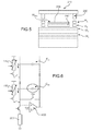
- Un exemple de dispositif microélectronique suivant l'invention, doté d'un capteur à bolomètre est donné sur la
figure 4 . - Ce dispositif comprend un substrat 201, par exemple un substrat semi-conducteur ou semi-conducteur sur isolant tel qu'un substrat SOI (SOI pour « silicon on insulator »), sur lequel une pluralité de composants électroniques, et de niveaux métalliques d'interconnexions superposés sont formés.
- Le dispositif peut comporter k (avec k un entier non nul) niveaux métalliques d'interconnexions superposés, chaque niveau comprenant une ou plusieurs lignes conductrices horizontales, parallèles au substrat 201 et un ou plusieurs éléments d'interconnexion verticaux, communément appelés « vias » permettant de relier des lignes conductrices de niveaux différents entre elles.
- Sur l'exemple de la
figure 4 , le dispositif comporte k = 6 niveaux métalliques d'interconnexions M1, M2, M3, M4, M5, M6 (les composants et les 3 premiers niveaux métalliques d'interconnexion M1, ..., M4, étant représentés de manière schématique par un bloc en traits discontinus au-dessus du substrat 201). - La partie sensible du capteur à bolomètre peut avoir un agencement tel que décrit précédemment en liaison avec la
figure 1 et être dotée d'une membrane 210 placée au dessus d'un empilement de couches reposant sur le support 201. La membrane 210 est suspendue au-dessus du support 200 qui est formé d'un empilement de couches reposant sur le substrat 201, et dans lequel la pluralité de niveaux d'interconnexions a notamment été réalisée. - Des plots conducteurs 230, servent à la fois à maintenir la membrane au dessus du substrat et à véhiculer des signaux électriques issus de la membrane et qui sont représentatifs d'une énergie thermique détectée.
- Une couche réfléchissante 260 de rayonnements électromagnétiques peut être prévue sur l'empilement, en regard de la membrane 210. La distance entre cette couche 260 et la membrane 210 est dictée par la hauteur des plots conducteurs 230, et peut être prévue en fonction de la longueur d'onde du rayonnement détecté.
- Le condensateur CI est un condensateur MIM pour (MIM pour « Métal Isolant Métal ») dont l'armature supérieure 244 est formée dans un niveau métallique d'interconnexion donné, par exemple dans le dernier niveau métallique M6 d'interconnexion, c'est-à-dire le niveau le plus éloigné du substrat 201.
- Selon une variante (
figure 5 ), le condensateur CI est doté d'une armature supérieure 246 formée dans un niveau métallique d'interconnexion M5bis, c'est-à-dire une couche métallique qui est située entre le niveau métallique M5 et le dernier niveau métallique M6 le niveau le plus éloigné du substrat 201, le niveau métallique d'interconnexion M5bis étant relié au dernier niveau M6. - L'armature inférieure 242 peut être formée dans un autre niveau métallique d'interconnexion, par exemple dans l'avant dernier niveau métallique M5 d'interconnexion.
- L'armature supérieure 244 et l'armature inférieure 242 peuvent être sous forme de zones métallique réalisées respectivement dans des couches isolantes 245 et 241.
- Les armatures supérieure 244 et inférieure 242 peuvent être formées par exemple à base de Cuivre ou d'aluminium et séparées entre elles par une couche isolante 243, qui peut être par exemple à base de SiO2.
- L'armature supérieure 244 du condensateur d'intégration CI peut être connectée à un comparateur (non représenté) par exemple à l'entrée inverseuse du comparateur, tandis que l'armature inférieure 244 est connectée à la sortie du comparateur.
- Sur les
figures 4 et5 , seule une cellule ou un pixel d'un dispositif microélectronique détecteur thermique, est représenté. Un tel dispositif comprend une pluralité de capteurs à bolomètre agencés selon une matrice et des moyens ou des circuits de lecture associés également arrangés selon une matrice en regard de la matrice des capteurs à bolomètre. - Selon une possibilité de mise en oeuvre (non représentée), le condensateur d'intégration CI peut être formé de plusieurs condensateurs montés en parallèle, par exemple de 3 capacités montés en parallèle.
- Dans ce cas, les condensateurs mis en parallèle peuvent être dotés chacun d'une armature supérieure formée dans le dernier niveau métallique M6, qui peut être connectée à au moins une autre armature supérieure d'un autre condensateur formé dans le dernier niveau métallique M6, et chacun d'une armature inférieure qui peut être formée dans l'avant dernier niveau métallique M5, et qui peut être connectée à au moins une autre armature inférieure d'un autre condensateur formé dans l'avant dernier niveau métallique M5.
- Selon une possibilité de mise en oeuvre, l'armature supérieure 244, du condensateur d'intégration peut appartenir à une piste métallique qui peut être partagée par plusieurs cellules et éventuellement par toutes les cellules d'une même colonne de la matrice.
- L'armature inférieure 242 du condensateur d'intégration CI peut également appartenir à une autre piste métallique qui peut être partagée par plusieurs cellules et éventuellement par toutes les cellules d'une même colonne de la matrice.
- Dans le cas où l'armature métallique supérieure 244 du condensateur d'intégration appartient à une piste métallique partagée par les cellules d'une même colonne de la matrice, cette armature peut en outre servir à acheminer le signal issu d'un capteur à bolomètre et faire office de bus de colonne. En acheminant le signal par l'armature la plus éloignée du substrat 201 et des composants formés sur ce dernier, on limite les phénomènes de couplage.
- Un tel agencement est donné par exemple sur la
figure 6 , sur laquelle des détecteurs à bolomètre 1101, ..., 110m appartenant à des cellules d'une même colonne d'un dispositif matriciel, sont représentés. - Un bolomètre de référence 200 est prévu par exemple en pied de colonne, tandis que le courant issu de la différence entre le courant provenant d'un bolomètre sensible et du courant provenant du bolomètre de référence est converti en tension grâce à un intégrateur, formé d'un comparateur 400 et de condensateurs d'intégration CI1, ...CIm mis en parallèles et dont les armatures font office de bus de colonne.
Claims (5)
- Dispositif microélectronique imageur thermique comprenant :- un support (200),- une pluralité de niveaux (M1, ..., M5, M6) métalliques d'interconnexions de composants électroniques formés sur le support,- une matrice de détecteurs thermiques formée sur le support, chaque détecteur comportant une membrane (210) permettant d'absorber une énergie rayonnante et de fournir un ou plusieurs signaux électriques en fonction de l'énergie rayonnante absorbée, et des moyens de lecture des signaux électriques issus de la membrane, les moyens de lecture étant intégrés au support,au moins plusieurs des dits détecteurs ayant des moyens de lecture dotés d'un intégrateur comprenant au moins un condensateur d'intégration (CI) formé en regard de la membrane, le condensateur ayant au moins une armature (244) supérieure réalisée dans un niveau métallique donné d'interconnexion de ladite pluralité de niveaux (M1, ..., M5, M6) métalliques d'interconnexions.
- Dispositif microélectronique selon la revendication 1, le condensateur MIM ayant au moins une armature (242) inférieure réalisée dans un autre des dits niveaux métalliques d'interconnexion.
- Dispositif microélectronique selon la revendication 1 ou 2, l'armature supérieure (242) étant connectée à un circuit de lecture par l'intermédiaire d'un ou plusieurs éléments d'interconnexions verticaux.
- Dispositif microélectronique selon l'une des revendications 1 à 3, une des armatures étant partagée par des détecteurs d'une même rangée de détecteurs de la matrice.
- Dispositif microélectronique selon la revendication 4, l'armature supérieure étant partagée par les détecteurs d'une même rangée de détecteurs de la matrice.
Applications Claiming Priority (1)
| Application Number | Priority Date | Filing Date | Title |
|---|---|---|---|
| FR0952033A FR2943783B1 (fr) | 2009-03-31 | 2009-03-31 | Pixel de bolometre dote d'un condensateur d'integration mim |
Publications (1)
| Publication Number | Publication Date |
|---|---|
| EP2237005A1 true EP2237005A1 (fr) | 2010-10-06 |
Family
ID=41323367
Family Applications (1)
| Application Number | Title | Priority Date | Filing Date |
|---|---|---|---|
| EP10157692A Withdrawn EP2237005A1 (fr) | 2009-03-31 | 2010-03-25 | Pixel de bolometre dote d'un condensateur d'integration mim |
Country Status (4)
| Country | Link |
|---|---|
| US (1) | US8426815B2 (fr) |
| EP (1) | EP2237005A1 (fr) |
| JP (1) | JP5667777B2 (fr) |
| FR (1) | FR2943783B1 (fr) |
Families Citing this family (11)
| Publication number | Priority date | Publication date | Assignee | Title |
|---|---|---|---|---|
| CN102564601A (zh) * | 2010-12-22 | 2012-07-11 | 精工爱普生株式会社 | 热式光检测装置、电子设备、热式光检测器及其制造方法 |
| US9679779B2 (en) | 2011-03-30 | 2017-06-13 | The Aerospace Corporation | Systems and methods for depositing materials on either side of a freestanding film using selective thermally-assisted chemical vapor deposition (STA-CVD), and structures formed using same |
| US9583354B2 (en) | 2011-03-30 | 2017-02-28 | The Aerospace Corporation | Systems and methods for depositing materials on either side of a freestanding film using laser-assisted chemical vapor deposition (LA-CVD), and structures formed using same |
| US10680021B2 (en) * | 2017-05-12 | 2020-06-09 | General Electric Company | Active pixel sensor computed tomography (CT) detector and method of readout |
| US10199424B1 (en) * | 2017-07-19 | 2019-02-05 | Meridian Innovation Pte Ltd | Thermoelectric-based infrared detector having a cavity and a MEMS structure defined by BEOL metals lines |
| US10923525B2 (en) | 2017-07-12 | 2021-02-16 | Meridian Innovation Pte Ltd | CMOS cap for MEMS devices |
| US10403674B2 (en) | 2017-07-12 | 2019-09-03 | Meridian Innovation Pte Ltd | Scalable thermoelectric-based infrared detector |
| US12168603B2 (en) | 2019-04-01 | 2024-12-17 | Meridian Innovation Pte Ltd | Monolithic post complementary metal-oxide-semiconductor integration of thermoelectric-based infrared detector |
| US11845653B2 (en) | 2019-04-01 | 2023-12-19 | Meridian Innovation Pte Ltd | Heterogenous integration of complementary metal-oxide-semiconductor and MEMS sensors |
| US12553776B2 (en) | 2020-05-28 | 2026-02-17 | Meridian Innovation Pte Ltd | Device having a metamaterial-based focusing annulus lens above a MEMS component and method of manufacturing thereof |
| CN116295862A (zh) * | 2022-09-07 | 2023-06-23 | 武汉高芯科技有限公司 | 一种非制冷红外探测器及其制作方法 |
Citations (3)
| Publication number | Priority date | Publication date | Assignee | Title |
|---|---|---|---|---|
| US5021663A (en) | 1988-08-12 | 1991-06-04 | Texas Instruments Incorporated | Infrared detector |
| US20040212001A1 (en) * | 2003-04-25 | 2004-10-28 | Sukehiro Yamamoto | Multilayer analog interconnecting line layout for a mixed-signal integrated circuit |
| US20050218520A1 (en) * | 2004-03-30 | 2005-10-06 | Nec Electronics Corporation | Semiconductor device and manufacturing method for the same |
Family Cites Families (7)
| Publication number | Priority date | Publication date | Assignee | Title |
|---|---|---|---|---|
| JP2734226B2 (ja) * | 1991-05-08 | 1998-03-30 | 日本電気株式会社 | 赤外線センサ |
| JPH05183135A (ja) * | 1991-10-14 | 1993-07-23 | Sony Corp | Ccd撮像装置 |
| JP3385762B2 (ja) * | 1994-12-12 | 2003-03-10 | 日産自動車株式会社 | 赤外線検知素子 |
| JP2002148342A (ja) * | 2000-11-07 | 2002-05-22 | Canon Inc | 放射線撮像装置 |
| US7554085B2 (en) * | 2003-10-09 | 2009-06-30 | Ocas Corp. | Bolometric infrared sensor having two-layer structure and method for manufacturing the same |
| JP2005188970A (ja) * | 2003-12-24 | 2005-07-14 | Matsushita Electric Ind Co Ltd | 熱型赤外線固体撮像装置および赤外線カメラ |
| FR2867273B1 (fr) * | 2004-03-04 | 2006-09-08 | Commissariat Energie Atomique | Procede de realisation d'un dispositif pour la detection thermique d'un rayonnement comportant un microbolometre actif et un microbolometre passif |
-
2009
- 2009-03-31 FR FR0952033A patent/FR2943783B1/fr not_active Expired - Fee Related
-
2010
- 2010-03-09 US US12/720,340 patent/US8426815B2/en not_active Expired - Fee Related
- 2010-03-25 EP EP10157692A patent/EP2237005A1/fr not_active Withdrawn
- 2010-03-30 JP JP2010078627A patent/JP5667777B2/ja not_active Expired - Fee Related
Patent Citations (4)
| Publication number | Priority date | Publication date | Assignee | Title |
|---|---|---|---|---|
| US5021663A (en) | 1988-08-12 | 1991-06-04 | Texas Instruments Incorporated | Infrared detector |
| US5021663B1 (en) | 1988-08-12 | 1997-07-01 | Texas Instruments Inc | Infrared detector |
| US20040212001A1 (en) * | 2003-04-25 | 2004-10-28 | Sukehiro Yamamoto | Multilayer analog interconnecting line layout for a mixed-signal integrated circuit |
| US20050218520A1 (en) * | 2004-03-30 | 2005-10-06 | Nec Electronics Corporation | Semiconductor device and manufacturing method for the same |
Also Published As
| Publication number | Publication date |
|---|---|
| US20100243892A1 (en) | 2010-09-30 |
| US8426815B2 (en) | 2013-04-23 |
| FR2943783A1 (fr) | 2010-10-01 |
| FR2943783B1 (fr) | 2011-06-10 |
| JP2010243490A (ja) | 2010-10-28 |
| JP5667777B2 (ja) | 2015-02-12 |
Similar Documents
| Publication | Publication Date | Title |
|---|---|---|
| FR2943783A1 (fr) | Pixel de bolometre dote d'un condensateur d'integration mim | |
| US7786440B2 (en) | Nanowire multispectral imaging array | |
| Tissot et al. | LETI/LIR's amorphous silicon uncooled microbolometer development | |
| US7943905B2 (en) | Infrared solid-state image sensor | |
| US7385199B2 (en) | Microbolometer IR focal plane array (FPA) with in-situ mirco vacuum sensor and method of fabrication | |
| FR2925159A1 (fr) | Dispositif pour la detection d'un rayonnement infrarouge comportant un bolometre resistif d'imagerie, systeme comprenant une matrice de tels bolometres, et procede de lecture d'un bolometre d'imagerie integre dans un tel system | |
| FR2983953A1 (fr) | Detecteur bolometrique d'un rayonnement electromagnetique dans le domaine du terahertz et dispositif de detection matriciel comportant de tels detecteurs | |
| FR2934044A1 (fr) | Detecteur bolometrique d'ondes electromagnetiques. | |
| WO2010112730A1 (fr) | Imagerie téra-hertz à convertisseur thermique perfectionné | |
| KR20190114028A (ko) | 편광 선택적, 주파수 선택적, 및 넓은 동적 범위의 검출기, 이미징 어레이, 판독 집적회로, 및 센서 시스템 | |
| JP2008268155A (ja) | 熱型赤外線固体撮像素子 | |
| WO2014091093A1 (fr) | Imageur monolithique multispectral visible et infrarouge | |
| FR2975529A1 (fr) | Circuit de detection a faible flux et faible bruit | |
| EP1174927B1 (fr) | Dispositif d'auto-compensation pour un système d'imagerie avec une architecture soustractive | |
| US9625312B2 (en) | Light sensor with correlated double sampling | |
| Hubbs et al. | Measurement of the radiometric and polarization characteristics of a microgrid polarizer infrared focal plane array | |
| CA3145264A1 (fr) | Capteur infrarouge a capture instantanee | |
| US7485860B2 (en) | Thermoelectric bridge IR detector | |
| FR2943415A1 (fr) | Procede de reglage d'un circuit de detection de rayonnements | |
| EP2517039B1 (fr) | Dispositif de detection de tache laser a ecartometre matriciel | |
| Jung et al. | Design and characteristics of a-Si-based micro-bolometers with shared-anchor structure in vacuum packaged systems | |
| FR3100886A1 (fr) | Capteur infrarouge et procede de commande associe | |
| WO2010035624A1 (fr) | Élément d'imagerie à semi-conducteurs | |
| FR2862160A1 (fr) | Dispositif de detection de rayonnements infrarouges a detecteurs bolometriques | |
| FR3141765A1 (fr) | Detecteur infrarouge multispectral |
Legal Events
| Date | Code | Title | Description |
|---|---|---|---|
| PUAI | Public reference made under article 153(3) epc to a published international application that has entered the european phase |
Free format text: ORIGINAL CODE: 0009012 |
|
| AK | Designated contracting states |
Kind code of ref document: A1 Designated state(s): AT BE BG CH CY CZ DE DK EE ES FI FR GB GR HR HU IE IS IT LI LT LU LV MC MK MT NL NO PL PT RO SE SI SK SM TR |
|
| 17P | Request for examination filed |
Effective date: 20110309 |
|
| STAA | Information on the status of an ep patent application or granted ep patent |
Free format text: STATUS: EXAMINATION IS IN PROGRESS |
|
| 17Q | First examination report despatched |
Effective date: 20161219 |
|
| STAA | Information on the status of an ep patent application or granted ep patent |
Free format text: STATUS: THE APPLICATION IS DEEMED TO BE WITHDRAWN |
|
| 18D | Application deemed to be withdrawn |
Effective date: 20200616 |