EP2229682B1 - A multi-energy imaging system and method using optic devices - Google Patents
A multi-energy imaging system and method using optic devices Download PDFInfo
- Publication number
- EP2229682B1 EP2229682B1 EP08859503.8A EP08859503A EP2229682B1 EP 2229682 B1 EP2229682 B1 EP 2229682B1 EP 08859503 A EP08859503 A EP 08859503A EP 2229682 B1 EP2229682 B1 EP 2229682B1
- Authority
- EP
- European Patent Office
- Prior art keywords
- optic
- ray
- energy
- multilayer
- layers
- Prior art date
- Legal status (The legal status is an assumption and is not a legal conclusion. Google has not performed a legal analysis and makes no representation as to the accuracy of the status listed.)
- Not-in-force
Links
Images


Classifications
-
- G—PHYSICS
- G21—NUCLEAR PHYSICS; NUCLEAR ENGINEERING
- G21K—TECHNIQUES FOR HANDLING PARTICLES OR IONISING RADIATION NOT OTHERWISE PROVIDED FOR; IRRADIATION DEVICES; GAMMA RAY OR X-RAY MICROSCOPES
- G21K1/00—Arrangements for handling particles or ionising radiation, e.g. focusing or moderating
- G21K1/06—Arrangements for handling particles or ionising radiation, e.g. focusing or moderating using diffraction, refraction or reflection, e.g. monochromators
- G21K1/062—Devices having a multilayer structure
-
- B—PERFORMING OPERATIONS; TRANSPORTING
- B82—NANOTECHNOLOGY
- B82Y—SPECIFIC USES OR APPLICATIONS OF NANOSTRUCTURES; MEASUREMENT OR ANALYSIS OF NANOSTRUCTURES; MANUFACTURE OR TREATMENT OF NANOSTRUCTURES
- B82Y10/00—Nanotechnology for information processing, storage or transmission, e.g. quantum computing or single electron logic
-
- G—PHYSICS
- G21—NUCLEAR PHYSICS; NUCLEAR ENGINEERING
- G21K—TECHNIQUES FOR HANDLING PARTICLES OR IONISING RADIATION NOT OTHERWISE PROVIDED FOR; IRRADIATION DEVICES; GAMMA RAY OR X-RAY MICROSCOPES
- G21K1/00—Arrangements for handling particles or ionising radiation, e.g. focusing or moderating
- G21K1/10—Scattering devices; Absorbing devices; Ionising radiation filters
-
- H—ELECTRICITY
- H01—ELECTRIC ELEMENTS
- H01J—ELECTRIC DISCHARGE TUBES OR DISCHARGE LAMPS
- H01J35/00—X-ray tubes
- H01J35/02—Details
- H01J35/16—Vessels; Containers; Shields associated therewith
-
- G—PHYSICS
- G21—NUCLEAR PHYSICS; NUCLEAR ENGINEERING
- G21K—TECHNIQUES FOR HANDLING PARTICLES OR IONISING RADIATION NOT OTHERWISE PROVIDED FOR; IRRADIATION DEVICES; GAMMA RAY OR X-RAY MICROSCOPES
- G21K2201/00—Arrangements for handling radiation or particles
- G21K2201/06—Arrangements for handling radiation or particles using diffractive, refractive or reflecting elements
- G21K2201/061—Arrangements for handling radiation or particles using diffractive, refractive or reflecting elements characterised by a multilayer structure
-
- G—PHYSICS
- G21—NUCLEAR PHYSICS; NUCLEAR ENGINEERING
- G21K—TECHNIQUES FOR HANDLING PARTICLES OR IONISING RADIATION NOT OTHERWISE PROVIDED FOR; IRRADIATION DEVICES; GAMMA RAY OR X-RAY MICROSCOPES
- G21K2201/00—Arrangements for handling radiation or particles
- G21K2201/06—Arrangements for handling radiation or particles using diffractive, refractive or reflecting elements
- G21K2201/064—Arrangements for handling radiation or particles using diffractive, refractive or reflecting elements having a curved surface
-
- G—PHYSICS
- G21—NUCLEAR PHYSICS; NUCLEAR ENGINEERING
- G21K—TECHNIQUES FOR HANDLING PARTICLES OR IONISING RADIATION NOT OTHERWISE PROVIDED FOR; IRRADIATION DEVICES; GAMMA RAY OR X-RAY MICROSCOPES
- G21K2201/00—Arrangements for handling radiation or particles
- G21K2201/06—Arrangements for handling radiation or particles using diffractive, refractive or reflecting elements
- G21K2201/067—Construction details
-
- H—ELECTRICITY
- H01—ELECTRIC ELEMENTS
- H01J—ELECTRIC DISCHARGE TUBES OR DISCHARGE LAMPS
- H01J2235/00—X-ray tubes
- H01J2235/18—Windows, e.g. for X-ray transmission
- H01J2235/183—Multi-layer structures
Definitions
- the invention relates generally to optics, and more particularly to multilayer optic devices and methods for making the same.
- EDXRD energy dispersive X-ray diffraction
- Such EDXRD systems may suffer from high false positives due to weak diffracted X-ray signals.
- the weakness of the X-ray signals may stem from a variety of origins.
- the polychromatic X-ray spectrum used in EDXRD is produced by the Bremsstrahlung part of the source spectrum, which is inherently low in intensity.
- X-ray source collimation may eliminate more than 99.99 percent of the source X-rays incident on the baggage volume under analysis.
- the materials being searched for may not diffract strongly as they are amorphous.
- the diffracting volume may be small. The last two limitations arise from the type of threat materials being searched for in baggage, making all but the second limitation unavoidable. Although discussed in the context of explosives detection, the limitations described above are equally applicable to medical situations.
- hollow glass polycapillary optics may be found in, for example, U.S. Patent No. 5,192,869 .
- the glass is the low index of refraction material, and air filling the hollow portions is the high index of refraction material.
- These types of optics typically do not provide much gain at energy levels above 80 keV, since the difference in the indices of refraction between air and glass becomes increasingly small as energy levels approach and surpass 80 keV.
- such optics use a concept of total internal reflection to reflect X-rays entering the hollow glass capillaries at appropriate angles back into the hollow capillaries, thereby channeling a solid angle of the source X-rays into collimated or focused beams at the output of the optic.
- the term "collimate” refers to altering the divergence of beams of electromagnetic (EM) radiation from the intrinsically divergent EM beams. Only about five percent of an EM source's solid angle typically is captured by the input of such known optics.
- the shaping of an X-ray spectrum to optimize it for particular applications is a common procedure.
- the change in the spectral shape for example, reducing either the relative proportion of low-energy X-rays or the relative proportion of high-energy X-rays, can in some cases provide for optimum imaging of a sample.
- One common artifact in radiographic and tomographic imaging arises from the fact that the lower energy X-rays in a typical Bremsstrahlung (polychromatic) spectrum are attenuated preferentially as the beam penetrates material. This effect, which leads to an increase in the mean energy of the beam as it penetrates the sample, introduces a biasing in the relationship between the strength of the transmitted beam and the amount of material penetrated.
- This biasing manifests as artifacts in any images reconstructed from the attenuation data, such as those attributed to beam hardening in computed tomography.
- Utilizing an X-ray beam that has a reduced spread of energies can mitigate some of these artifacts.
- beam intensity with respect to the intensity in that same range of the original spectrum, has been held constant or augmented by the use of the optic
- the use of a limited range of energies can provide a desired degree of attenuation for a particular application and can produce an optimum image in terms of spatial resolution and contrast sensitivity.
- the shaping of a spectrum from a polychromatic energy distribution to a more monochromatic distribution can enable such improvements in X-ray image sets.
- Spectral imaging also includes a single energy distribution as well as multi-energy distributions.
- Multi-energy X-ray imaging sometimes referred to as dual-energy imaging or energy discrimination imaging, has been shown to furnish information on specific material compositions in scanned objects for security, industrial, and medical applications.
- Such energy discrimination imaging can be achieved in several ways, including the use of two or more different X-ray spectra, which is often the most feasible approach.
- a challenge lies in the sequential nature of such an examination, where image data are generated, for example, first with one spectrum and then with another spectrum.
- an object of interest is scanned twice.
- a first complete projection data set is produced in the first scan for one energy and then a second complete projection data set is produced in the second scan for the second energy.
- sample composition is dynamic, and/or sample positioning may preclude repetitive scanning, the logistics of physically scanning an object twice may be unacceptable.
- WO01/08162 discloses an X-ray collimator comprising a multilayer reflector shell that consists of a gapless stack of conformal layers of different indices of refraction.
- US4684565 discloses that rough surfaces attenuate the reflection of higher order harmonics of X-rays.
- the invention refers to an optic assembly according to the subject-matter of claim 1.
- the invention also relates to a method for forming a low-energy spectrum image according to the subject-matter of claim 2.
- FIG. 1 is a schematic view illustrating the phenomenon of total internal reflection.
- FIG. 2 is a top schematic view of an optic device constructed in accordance with an embodiment of the invention.
- FIG. 3 is a cross-sectional view of the optic device of FIG. 2 taken along line III-III.
- FIG. 4 is an end view of the optic device of FIG. 2 .
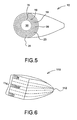
- FIG. 5 is a perspective view of the optic device of FIG. 2 .
- FIG. 6 is a perspective view of an optic device constructed in accordance with an embodiment of the invention.
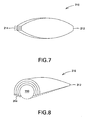
- FIG. 7 is a perspective view of an optic device constructed in accordance with an embodiment of the invention.
- FIG. 8 is a perspective view of an optic device constructed in accordance with an embodiment of the invention.
- FIG. 9 is a perspective view of an optic device constructed in accordance with an embodiment of the invention.
- FIG. 10 is a perspective view of an optic device constructed in accordance with an embodiment of the invention.
- FIG. 11 is a perspective view of an optic device constructed in accordance with an embodiment of the invention.
- FIG. 12 is a perspective view of an optic device constructed in accordance with an embodiment of the invention.
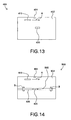
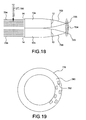
- FIG. 13 is a schematic view of a deposition assembly constructed in accordance with an embodiment of the invention.
- FIG. 14 is a schematic view of a deposition assembly constructed in accordance with an embodiment of the invention.
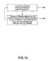
- FIG. 15 illustrates process steps for fabricating an optic device in accordance with an embodiment of the invention.
- FIG. 16 is a block diagram of a conventional computed tomography system.
- FIG. 17 is a cross-sectional view of an X-ray tube head using an optic in accordance with an embodiment of the invention.
- FIG. 18 is a schematic view of a pair of optic devices for use with a target in a dual energy scanning system in accordance with an embodiment of the invention.
- FIG. 19 is a schematic view of a filter wheel for use with the optic devices of FIG. 18 .
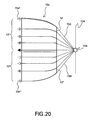
- FIG. 20 is a schematic view of a spliced optic device for use with a target in a dual energy scanning system in accordance with an embodiment of the invention.
- Embodiments of the invention described herein primarily utilize the phenomenon of total internal reflection.
- total internal reflection when an angle of incidence is less than a critical angle ⁇ c , total internal reflection occurs.
- the critical angle ⁇ c for total internal reflection depends on, among other factors, the selection of materials, the difference in the relative indices of refraction between the materials, the material photon absorption properties, and the energy of the incident photons.
- the critical angle ⁇ c can be increased several times over an air-glass critical angle, allowing many more photons to satisfy the condition for total internal reflection. This will allow a greater photon transmission through a multilayer optic than is possible with, for example, polycapillary optics.
- multilayer optic 10 including an input face 12 and an output face 14.
- multilayer is meant a structure that has a plurality of layers with each layer having a single composition.
- the multilayer optic 10 includes multiple layers of material, each having a different index of refraction. For example, there are layers 16, 20, and 24 surrounding a core 50. Layer 15, formed of a lower index of refraction material, is positioned radially exterior to and contiguous with the core 50.
- the core 50 may be formed of a higher index of refraction material such as beryllium, lithium hydride, magnesium, or any other suitable elements or compounds having similarly higher refractive indices and high X-ray transmission properties.
- the core 50 may be less than a micrometer to greater than one centimeter in diameter.
- Layer 20 is positioned radially exterior to layer 16 and radially interior to layer 24.
- the layers making up the multilayer optic 10 may be formed of materials that have varying indices of refraction.
- layers 15, 19, 23, and 27 may be formed of materials that have a lower index of refraction and a high X-ray absorption.
- appropriate materials may be chosen from osmium, platinum, gold, or any other suitable elements or compounds having similarly lower refractive indices and high X-ray absorption properties.
- the core 50 and layers 16, 20, and 24 may be formed of materials having a higher index of refraction and a high X-ray transmission.
- appropriate materials may be chosen from beryllium, lithium hydride, magnesium, or any other suitable elements or compounds having similarly higher refractive indices and high X-ray transmission properties.
- the diameter of the core 50 is computed by considering the location of the X-ray radiation source focal point relative to the input face of the optic and the required critical angle for total internal reflection between the higher index of refraction of the core 50 and the lower index of refraction of the layer 15.
- the multilayer optic 10 can utilize the principle of total internal reflection of electromagnetic radiation. Specifically, diverging electromagnetic radiation beams 38, 40, and 42 stemming from an electromagnetic radiation source 34 enter the input face 12 and are redirected by the principle of total internal reflection into quasi-parallel beams of photons 44 exiting the output face 14.
- Multilayer optics in accordance with embodiments of the invention can collect a large solid angle of an X-ray source 34 and redirect photons containing polychromatic energies into quasi-parallel photon beams.
- Quasi-parallel means that diverging beams of photons, such as X-rays, have been collected and focused into beams of electromagnetic radiation or X rays to exit the output face 14 at or below the critical angle ⁇ c . This divergence causes the intrinsic source X-ray beam to be larger than the output face 14 of the optic 10 and larger than the parallel beam of X rays produced by the optic.
- multilayer optics in accordance with embodiments of the invention may be configured to produce slightly focused, highly focused, slightly diverging, or highly diverging beams.
- lightly focused is meant that the beam size at the point of interest (i.e., where the diameter of the beam is of concern) is approximately the same as the beam at the output face 14 of the optic 10.
- highly focused is meant that the beam size at the point of interest is smaller than the beam at the output face 14 of the optic 10.
- lightly diverging is meant that the beam size is larger than a quasi-parallel beam but smaller than the intrinsic source beam.
- highly diverging is meant that the beam is the same size or larger than the intrinsic source beam.
- intrinsic source beam is meant to represent an X-ray beam emitted from the source housing with no optic in the beam.
- the composition of materials making up the multilayer optic 10, the macroscopic geometry of the multilayer optic 10, the thickness of the multilayer optic 10, and the number of individual layers determine the angular acceptance range of the multilayer optic 10.
- the angular acceptance range may be from about 0 steradians up to about 2 ⁇ steradians of a solid angle of a photon source.
- only a few layers have been illustrated with reference to multilayer optic 10. However, it should be appreciated that any number of layers, including into the hundreds, thousands, or millions of layers, can be fabricated to utilize total internal reflection to form the various types of photon beams listed previously.
- the core 50 and the layers 16, 20, 24 may have photon, or X-ray, redirection regions.
- layer 16 has a photon redirection region 17 stemming from a center of curvature
- layer 20 has a photon redirection region 21 stemming from a second center of curvature
- layer 24 has a photon redirection region 25 stemming from yet another center of curvature.
- the photon redirection regions 17, 21, 25 are chosen to allow for the diverging electromagnetic radiation beams 38, 40, and 42 to be made parallel or near parallel to beam 36, or conversely to allow for parallel or converging electromagnetic radiation beams to be made diverging.
- the minimum photon redirection region is determined by the minimum thickness that would still enable a smooth surface, which is at least two atomic layers, or about ten angstroms.
- the photon redirection regions 17, 21, 25 each contain redirecting segments.
- the redirecting segments are chosen such that they each have a constant curvature.
- the curvature of each redirecting segment may be the same as or different from the curvatures of other redirecting segments. If each of the redirecting segments for a particular photon redirection region is straight, then the radius of curvature is infinite.
- the photons or electromagnetic radiation 38, 40, 42 entering the input face 12 can be redirected into quasi-parallel pencil beams 44, thereby increasing the photon flux density at the output face 14 over the photon flux density in the direct source beam (X-ray beam without the optic) at the same distance from the source 34.
- the output face 14 may be formed closer to the input face 12, i.e., positioned prior to the region where the photons are redirected into parallel rays, allowing the input electromagnetic radiation beams 38, 40, 42 to remain somewhat diverging as they exit the output face 14. It should further be appreciated that core 50 and any number of the layers may have no arc of curvature, instead having a cylindrical cross-sectional profile.
- this optic 10 An important feature of this optic 10 is that the X-ray transmitting layers, for example, layers 16, 20, 24, can be made thin enough - on the order of a few nanometers - that the solid angle of source photons collected by these layers are small enough to accept almost all the X-rays entering the layers, i.e. the X-ray trajectories satisfy the critical angle condition for total internal reflection.
- This is unlike known optics, where the X-ray transmitting regions are on the order of microns thick and a significant number are absorbed at the reflecting interface because the photon trajectories do not satisfy the critical angle condition for total internal reflection.
- the X-ray absorption layers are orders of magnitude thinner than in known optics making the X-ray transmission of known optics orders of magnitude smaller than the optics described in this application.
- the overall optic length (from input face 12 to output face 14) is short enough that photon losses are minimal.
- the multilayer optic 10 can be utilized in applications that operate at energy levels above 60 keV, such as, for example, X-ray diffraction, medical and industrial CT imaging, medical and industrial X-ray, and cargo inspection, to name a few. Some of these applications may operate at energy levels as high as 450 keV.
- a multilayer optic 110 including a plurality of layers 113a - 113n, one on top of the other, extending between an input face 112 and an output face 114 having a polygonal profile.
- the middle layer of the multilayer optic 110 is layer 113mid. Except for layer 113mid, all of the layers include a photon redirection region positioned between the input face 112 and the output face 114. It should be appreciated, however, that layer 113mid may include a photon redirection region, or that other layers in addition to 113mid may lack a photon redirection region.
- the design shown allows diverging electromagnetic radiation to be input into the input face 112, redirected by the optic multilayers, and output from the output face 114 into a reduced cone beam, such as, for example, a reduced cone fan beam.
- a reduced cone beam such as, for example, a reduced cone fan beam.
- the fan beams may be parallel or near parallel or may be somewhat divergent but still focused relative to the input electromagnetic radiation.
- the conformal nature of the individual layers allows for the multilayer optic 110 to be utilized in a vacuum environment.
- a multilayer optic 210 that includes an input face 212 and an output face 214.
- the multilayer optic 210 includes individual layers sandwiching a mid-layer. The design shown allows for a focused fan beam output. As with the previously described embodiments, the conformal nature of the individual layers allows the multilayer optic 210 to be used in a vacuum environment.
- FIG. 8 illustrates a multilayer optic 310 having an input face 312 and an output face 314.
- the layers have been positioned over a cone 150, which serves as a blank or mold for the individual layers.
- the output beam exiting the output face 314 is shaped into a curved output, which can be coupled to a singly curved diffracting crystal (not shown) to enable the creation of a cone beam of highly monochromatic radiation.
- Monochromatic radiation is used in several different applications, including, for example, X-ray diffraction. Highly monochromatic radiation is radiation within a very narrow energy range approximately equal to that produced by diffracting from a single crystal.
- the curved diffracting crystal can be formed of any suitable material, such as, for example, mica, silicon, germanium, or platinum and curved so that the crystal conforms to the surface of, for example, a cone or cylinder.
- suitable material such as, for example, mica, silicon, germanium, or platinum
- the suitability of any material for use as the diffracting crystal is dependent upon the diffraction intensity and the lattice spacing of the material. It should be appreciated that the multilayer optic 310 should be positioned between the source of the electromagnetic radiation and the diffracting crystal to obtain the maximum photon flux density in the diffracted beam.
- Quasi-monochromatic radiation is radiation within a limited wavelength range that is greater than the highly monochromatic range but less than the full Bremsstrahlung spectrum from an X-ray source.
- FIGS. 9-12 illustrate various other potential embodiments of multilayer optics.
- FIGS. 9 and 10 illustrate multilayer optics that have output faces in a photon redirection region, thereby allowing such optics to emit highly diverging beams.
- FIGS. 11 and 12 illustrate multilayer optics whose output faces are dimensionally smaller than their respective input faces, allowing such optics to emit highly focused beams.
- a multilayer optic deposition assembly 400 including a deposition chamber 402 and a movable shutter apparatus 410.
- the deposition chamber 402 may be utilized in suitable deposition techniques, including, for example, vapor deposition, or thermal spray deposition.
- suitable vapor deposition techniques include sputtering, ion implantation, ion plating, laser deposition, evaporation, and jet vapor deposition.
- Evaporation techniques may include thermal, electron-beam, or any other suitable technique resulting in appreciable deposition of material.
- Suitable thermal spray deposition includes combustion, electric arc, and plasma spray.
- the deposition chamber 402 includes an inputting apparatus 404 for allowing ingress of deposition materials into the deposition chamber 402. It should be appreciated that the inputting apparatus 404 may include numerous inlet nozzles, each being associated with a specific deposition material.
- a blank 420 is positioned within the deposition chamber 402. The blank 420 may be a core 50 or a cone 150, described previously with regard to the embodiments illustrated in FIGS. 4 and 8 , or it may be a substrate serving as a support mechanism for deposited layers. It should be appreciated that the blank 420 can assume virtually any suitable geometric configuration consistent with the desired beam profile. Examples of the almost infinite number of suitable geometric configurations include a circular wafer, a rectangular prism, a cone, a cylinder, and an egg-shape, to name a few.
- the shutter apparatus 410 enables the formation of a multilayer optic wherein the individual layers have a photon redirection region. Specifically, as a deposition material is input into the deposition chamber 402 through the inputting apparatus 404, the shutter apparatus 410 moves in a direction A relative to the blank 420. If the speed of the shutter apparatus 410 decreases as it moves in the direction A, an increasing amount of deposition material will contact the blank 420 in the direction A, thereby enabling the formation of a multilayer optic with individual layers having different thicknesses and having photon redirection regions. Control of the movement and velocity of the shutter apparatus 410 may be accomplished electronically with a digital controlling mechanism, such as a microcontroller, microprocessor, or computer. Alternatively, control of the movement may be accomplished manually, or mechanically, such as, pneumatically, hydraulically, or otherwise.
- the individual layers can be deposited upon the blank 420, and a multilayer optic having conformal individual layers, like the multilayer optic 110 shown in FIG. 6 , can be formed.
- a multilayer optic like the multilayer optic 110
- the first layer to be laid down may be the layer adjacent to mid-layer 113mid.
- the subsequent layers leading to and including layer 113a can be deposited.
- the partially formed multilayer optic can be turned over and the layers leading to and including layer 113n can be deposited.
- a multilayer optic like the multilayer optic 210 shown in FIG. 7 can be formed. It should be appreciated that the deposition rate of the deposition material in the deposition chamber 402 may be altered as well.
- a multilayer optic deposition assembly 500 that includes a deposition chamber 502 and the movable shutter 410.
- the deposition chamber 502 includes the apparatus 404 that is the source of a vapor stream and a pair of rotatable spindles 505.
- the spindles 505 are capable of rotating in a direction B. Further, the spindles 505 each include a pointed end that comes into contact with and holds the blank 420. By rotating the spindles 505 in the same direction B the blank 420 can be rotated while deposition material is introduced into the deposition chamber 502 through the inputting apparatus 404.
- Movement of the shutter apparatus 410 in the direction A and rotation of the blank 420 in the direction B will enable the formation of a multilayer optic such as the multilayer optic 10 shown in FIG. 5 .
- the spindles 505 can remain in a non-rotating state during a first set of deposition steps to form the layers adjacent to layers 113mid to 113a in FIG. 6 . Then, the spindles 505 can be rotated to turn the partially formed multilayer optic one hundred and eighty degrees around to allow for a second set of deposition steps to form the layers leading to and including 113n to form the multilayer optic 110.
- the inputting apparatus 404 may be kept stationary, with its vapor beams focused to different heights along the blank 420.
- the resulting different deposition rates will create the depth and laterally graded inputs and outputs on the optic and will enable the formation of a multilayer optic such as the multilayer optic 10 shown in FIG. 5 .
- FIG. 15 illustrates process steps for forming a multilayer optic.
- a material having a pre-determined index of refraction with a pre-determined photon transmission coefficient is deposited.
- the material is deposited on a blank or substrate, which may be a core, a cone, or a polygonal support mechanism. It should be appreciated that the blank or substrate may be incorporated within the multilayer optic, such as the core 50, or may serve merely as a mold, like cone 150.
- another material having a prescribed index of refraction with a photon transmission coefficient is deposited onto the previous material in such a way as to be conformal and have minimal void spaces.
- each individual layer may be formed at thicknesses in the range of one nanometer to thousands of nanometers.
- the Steps 600 and 605 can be sequentially repeated to prepare, for example, multiple pairs of layers, with each pair having one layer having a first index of refraction with a first photon transmission coefficient and a second layer having a second index of refraction with a second photon transmission coefficient.
- the deposition of the first and second materials may be accomplished by any number of suitable processes, such as, for example, vapor deposition, thermal spray deposition, or electroplating.
- suitable vapor deposition techniques include sputtering, ion implantation, ion plating, laser deposition (using a laser beam to vaporize a material or materials to be deposited), evaporation, or jet vapor deposition (using sound waves to vaporize a material or materials to be deposited).
- evaporation techniques may be thermal, electron-beam or any other suitable technique that will result in appreciable deposition of material.
- suitable thermal spray deposition techniques include combustion, electric arc, and plasma spray.
- the partially formed multilayer optic may be rotated, oscillated, or moved. It may be turned, and it may be subjected to a deposition process whereby the deposition material is deposited at different rates along the axis of the multilayer optic.
- multilayer optics can be formed with various configurations and profiles that will allow for a greater amount of electromagnetic radiation to be collected from a source at the input of the optic, parallel or near parallel beams of electromagnetic radiation to be output from the multilayer optic, or beams of electromagnetic radiation output from the multilayer optic to be shaped into pencil beams, cone beams, fan beams, or curved in an arc, as an example.
- Multilayer optics in accordance with embodiments of the invention may be used in various industrial applications.
- a multilayer optic formed to emit a quasi-parallel beam having a circular cross-section may find utility in X-ray diffraction and backscatter applications, such as non-destructive examination.
- a multilayer optic formed to emit a slightly focused beam with a circular cross-section may find utility in X-ray diffraction, X-ray fluorescence, medical diagnostic or interventional treatments, and non-destructive examination applications.
- Multilayer optics formed to emit a highly focused beam having a circular cross-section may find utility in X-ray fluorescence; medical diagnostic or interventional treatments of, for example, small tumors; and, non-destructive examination applications.
- Multilayer optics formed to emit a slightly diverging beam having a circular cross-section may find utility in computed tomography and X-ray diagnostic system applications.
- Multilayer optics formed to emit a highly diverging beam having a circular cross-section may find utility in non-destructive examination applications requiring an increased field-of-view, and in medical diagnostic or interventional imaging and treatments requiring an increased field-of-view, such as the imaging and treatment of large tumors.
- multilayer optics formed to emit a variety of beam shapes is in medical interventional treatments, such as treatment of tumors, where the optic shape is determined by the tumor shape.
- Such multilayer optics would allow X rays to be focused onto the tumor without irradiating nearby healthy tissue, providing targeted treatment with a minimum of damage to surrounding healthy tissue.
- Multilayer optics formed to emit a fan beam in one plane that is quasi-parallel, slightly focusing, highly focusing, slightly diverging, or highly diverging in a direction transverse to the plane may find utility in computed tomography, X-ray diagnostic system, and non-destructive examination applications.
- the fan beam may have a divergence the same as or greater than that of the source.
- multilayer optics formed to emit a quasi-parallel fan beam in one plane that is quasi-parallel, slightly focused, highly focused, slightly diverging, or highly diverging within the plane of the fan would produce a beam having a rectangular cross-section that may find utility in computed tomography, as well as non-destructive and medical examination applications.
- Multilayer optics formed to emit a fan beam in one plane that is slightly or highly diverging in the direction transverse to the fan beam plane may find utility in medical interventional applications, such as close-up imaging to increase field-of-view.
- the divergence in the direction transverse to the fan beam plane is equal to or greater than the source divergence.
- Multilayer optics formed to emit a fan beam in one plane that is quasi-parallel, slightly focusing, highly focusing, slightly diverging, or highly diverging perpendicular to the plane of the fan may find utility in computed tomography, X-ray diagnostic system, and non-destructive examination applications.
- the fan beam may have a divergence the same as or greater than that of the source.
- a multilayer optic coupled to a diffracting crystal may produce a quasi-parallel monochromatic fan beam that may find utility, provided the intensity is great enough, in medical imaging and interventional treatments.
- Such monochromatic imaging would reduce a patient's dose of X-rays while increasing the resolution, for example, by reducing cone beam artifacts, and reducing streaking/shading such as those incurred with beam hardening effects.
- FIG. 16 illustrates a conventional acquisition system 700 for use in an object detection system, such as, for example, a computed tomography (CT) scanner.
- the acquisition system 700 comprises a scanner 702 formed of a support structure and internally containing one or more stationary or rotationally distributed sources of X-ray radiation (not shown in FIG. 16 ) and one or more stationary or rotational digital detectors (not shown in FIG. 16 ), as described in greater detail below.
- the scanner 702 is configured to receive a table 704 or other support for an object to be scanned, such as, for example, baggage or luggage or patients.
- the table 704 can be moved through an aperture in the scanner to appropriately position the subject in an imaging volume or plane that is scanned during imaging sequences.
- the system further includes a radiation source controller 706, a table controller 708 and a data acquisition controller 710, which may all function under the direction of a system controller 712.
- the radiation source controller 706 regulates timing for discharges of X-ray radiation which is directed from points around the scanner 702 toward a detector element on an opposite side thereof, as discussed below.
- the radiation source controller 706 may trigger one or more emitters in a distributed X-ray source at each instant in time for creating multiple projections or frames of measured data.
- the X-ray radiation source controller 706 may trigger emission of radiation in sequences to collect adjacent or non-adjacent frames of measured data around the scanner.
- data acquisition controller 710 coupled to detector elements as described below, receives signals from the detector elements and processes the signals for storage and later image reconstruction.
- source controller 706 may also direct rotation of a gantry on which the distributed source or sources are mounted. Operation of the gantry also may be controlled by the system controller 712 or a separate controller altogether.
- Table controller 708, then, serves to appropriately position the table and subject in a plane in which the radiation is emitted, or, in the present context, or generally within a volume to be imaged. The table may be displaced between imaging sequences or during certain imaging sequences, depending upon the imaging protocol employed.
- data acquisition controller 710 may also direct rotation of a gantry on which the detector or detectors are mounted.
- System controller 712 generally regulates the operation of the radiation source controller 706, the table controller 708 and the data acquisition controller 710.
- the system controller 712 may thus cause radiation source controller 706 to trigger emission of X-ray radiation, as well as to coordinate such emissions during imaging sequences defined by the system controller.
- the system controller may also regulate movement of the table in coordination with such emission to collect measurement data corresponding to volumes of particular interest, or in various modes of imaging, such as helical modes.
- system controller 712 coordinates rotation of a gantry on which the source(s), detector(s), or both are mounted.
- the system controller 712 also receives data acquired by data acquisition controller 710 and coordinates storage and processing of the data.
- controllers may be defined by hardware circuitry, firmware or software. Moreover, the controllers may be separate pieces of hardware, as shown in FIG. 16 , or integrated into one piece of hardware.
- the particular protocols for imaging sequences will generally be defined by code executed by the system controllers.
- initial processing, conditioning, filtering, and other operations required on the measurement data acquired by the scanner may be performed in one or more of the components depicted in FIG. 16 .
- detector elements will produce analog signals representative of depletion of a charge in photodiodes positioned at locations corresponding to pixels of the data acquisition detector. Such analog signals are converted to digital signals by electronics within the scanner, and are transmitted to data acquisition controller 710. Partial processing may occur at this point, and the signals are ultimately transmitted to the system controller for further filtering and processing.
- System controller 712 is also coupled to an operator interface 714 and to one or more memory devices 716.
- the operator interface may be integral with the system controller, and will generally include an operator workstation for initiating imaging sequences, controlling such sequences, and manipulating measurement data acquired during imaging sequences.
- the memory devices 716 may be local to the imaging system, or may be partially or completely remote from the system. Thus, imaging devices 716 may include local, magnetic or optical memory, or local or remote repositories for measured data for reconstruction. Moreover, the memory devices may be configured to receive raw, partially processed or fully processed measurement data for reconstruction.
- a monitor (not shown) may also be connected to operator interface 714 to allow viewing of scan data, reconstruction data, or otherwise processed data.
- System controller 712 or operator interface 714, or any remote systems and workstations may include software for image processing and reconstruction.
- processing of CT measurement data may be performed by a number of mathematical algorithms and techniques.
- conventional filtered back-projection techniques may be used to process and reconstruct the data acquired by the imaging system.
- Other techniques, and techniques used in conjunction with filtered back-projection may also be employed.
- a remote interface 718 may be included in the system for transmitting data from the imaging system to such remote processing stations or memory devices.
- FIG. 17 illustrates a portion of an acquisition subsystem 800 for use in an object detection system, such as, for example, a computed tomography (CT) scanner such as the scanner 702 of FIG. 16 .
- CT computed tomography
- FIG. 17 illustrates an X-ray tube head 840.
- a multilayer optic 10 is incorporated within the system 800.
- the alternating lower and higher index of refraction materials with concurrent high and low X-ray absorption properties, respectively, in contiguous layers, of a multilayer optic 10 utilize the principle of total internal reflection of electromagnetic radiation.
- diverging X-ray beams emanating from the target 724 enter the input face 12 and are redirected into beams of photons 734 exiting the output face 14.
- the multilayer optic 10 can be formed to output any desired beam.
- the multilayer optic 10 can be positioned exterior or interior to the window 748.
- the multilayer optic 10 is shown in both locations in FIG. 17 for ease of illustration.
- the multilayer optic 10 may be formed in such a way as to produce a desired shaped beam of X-rays at energies of 20 keV and above depending on the application, such as the beams of photons 734 shown in FIG. 17 .
- the multilayer optic 10 for producing a limited cone beam of X-rays can be formed as described above with reference to FIGS. 2-5 , with the exception being that the output face 14 is formed closer to an input face 12, i.e., positioned prior to the region where the photons are redirected into parallel rays.
- the input face 12 may be flat or it may be curved to accept as much of the source cone of X-rays from the target 724. This allows the input X-ray beams to be shaped into a desired shaped beam 734.
- a third-generation CT imaging system where the X-ray tube and detector rotate about the imaging volume has been described herein; however, the optic is equally applicable to alternate configurations of third-generation technology, for example, with industrial CT configurations where the X-ray source and detector are held fixed and a stage rotates the object during data acquisition.
- FIG. 18 there is shown a pair of optic devices 10 a , 10 b .
- Each of these optic devices 10 a , 10 b is similar to the optic device 10 described with specific reference to FIGS. 2-5 .
- the difference between the optic devices 10 a , 10 b is that one is formed to pass higher X-ray energies, while the other is formed to pass lower X-ray energies.
- Shaping or filtering the source spectrum with the optic devices 10 a , 10 b offers the promise of rapidly producing spectral shapes with sharp higher-energy cutoffs on a sub-view basis, which improves material separation sensitivity and can eliminate most registration issues.
- the capabilities for producing spectra with desired spectral shapes and for producing them on a fast time scale makes such optic devices particularly useful for multi-energy imaging.
- K-edge filters may be utilized to provide a sharp low-energy cut-off for each optic 10 a , 10 b .
- One set-up includes vapor depositing the K-edge filter directly onto either end of the optic 10 a , 10 b .
- the K-edge filter may be formed as a separate foil aligned with the output or input of the optic 10 a , 10 b . Then each optic 10 a , 10 b would have its own different K-edge filter either integral to the optic or separate from it.
- the optic devices 10 a , 10 b which as illustrated may be in a stacked arrangement, are in optical communication with the target 724 of the X-ray tube head 840 of the acquisition subsystem 800 ( FIG. 17 ). Specifically, X-rays 733 formed by striking electron beams at focal spots 725 on the target 724 are propagated from the focal spots 725 toward the input faces 12 of the optic devices 10 a , 10 b . Alternatively, the focal spots 725 may each be within separate individual target spots as opposed to the single continuous target spot 724 or on separate non-contiguous targets. The X-rays 733 are then focused by the optical devices 10 a , 10 b , as described above, and exit the output faces as redirected X-rays 734. This geometry can be replicated to produce an array of pairs of such spots, where a distributed array of x-ray source spots is to be utilized.
- One such arrangement uses an optic device with a separate K-edge filter to produce two signals whose energy distributions are different from each other. This is done by taking an image with one optic device and then retaking the image with both the optic device and a K-edge filter to eliminate low energy photons. Subtracting the two, appropriately normalized, signals results in a signal with predominantly low energies, while the signal produced by the combined optic device and K-edge filter produces a signal with relatively higher energy photons.
- two optic devices could be used in conjunction with at least one K-edge filter.
- the two optic devices are made of materials that result in x-ray redirection and transmission of two photon energy ranges that may or may not overlap. Taking an image with these two optic devices, repeating with the optic devices and a K-edge filter that blocks the energies from the optic device that transmits the lower energies, and subtracting the two, appropriately normalized, images will result in an image derived from only the low energies passed by the optic that transmitted the lower energies.
- the lower energy spectrum image could be obtained by subtracting this higher energy spectrum image, appropriately normalized, from the image formed with photons from the combined two optic devices and K-edge filter.
- a second K-edge filter could be included that blocks the lowest energy photons from that optic.
- Another option that can provide even greater energy separation between the signals is to couple the optic devices to separate targets at different accelerating potentials and taking sequential images with x rays emitted by each accelerating potential/optic combination.
- a filter wheel 775 may be used for sequential filtering of the signals.
- the filter wheel 775 could be made to include portions 780 that are opaque to all photons and windows 782 that are transparent to all the X rays.
- the windows 782 are only illustrated partially around the filter wheel 775 for ease of illustration purposes only.
- the windows 782 could be covered by appropriate filtering material, such as that needed to block the low-energy X rays from the higher-energy spectrum when two optic devices are used for imaging.
- a portion 780 can be positioned between the optic device 10 a and the detector, thereby blocking all the X rays transmitted by the optic 10 a from reaching the detector.
- a window 782 can be positioned between the other optic device 10 b and the detector, allowing all the X rays transmitted by optic 10 b to reach the detector.
- the filter wheel 775 is rotated to allow a window 782 to be positioned between the optic device 10 a and the detector 750, and a portion 780 is positioned between the optic device 10 b and the detector 750, allowing X rays from only optic device 10 a to be received by the detector.
- the optic devices 10 a , 10 b are fabricated such that each filters out certain X-ray energy levels. Specifically, each optic device 10 a , 10 b is fabricated from appropriate optic materials that selectively redirect X-rays of a certain energy level in the optic by predominantly total internal reflection. The refractive indices of the materials used to fabricate the optic devices determine the high-energy cutoff, establishing the emitted spectrum high-energy endpoint.
- the optic devices include alternating high and low refractive index materials deposited in layers, with individual layers being in the nanometer thickness range.
- Each layer at the input face 12 of an optic device 10 may be curved to a different degree to capture a large source angle, such as, forty-five degrees or more, and redirect the X-rays into a tightly collimated fan-shaped beam.
- combining some sort of low energy x-ray filtering, such as K-edge filters, with the higher-energy filtration of the optic devices 10 a , 10 b different spectral shapes can be produced effectively.
- the low energy filtering can take the form of stand-alone foils that can be placed in the conventional post-optic emission position, or between the source focal spot and the optic devices.
- these low-energy filters can be vapor-deposited or chemically plated onto either the input or output ends of each optic.
- Another possibility is to incorporate the filter internally to the optic devices as a dopant in the high refractive index materials.
- a method for filtering the lower energies from an optic's transmission in accordance with the present invention is to manufacture the optic with selectively rough interfaces. The surface roughness will cause the highest energies to be scattered, while not affecting the reflection of the lower energies.
- a method for internally filtering includes choosing different materials in the optic device that determine the critical angle for total internal reflection, wherein the critical angle determines the highest X-ray energies transmitted by the optic device. The energy spectra produced by these optics-filter alternatives can be shaped considerably different from the source's inherent Bremsstrahlung emission, with much sharper high and low-energy cutoffs.
- FIG. 20 Another topology for creating two different energy distribution images is shown in FIG. 20 involving splicing together two halves 10', 10" of two different optics to form a single optic device 10 c .
- the creation of a single optic device 10 c of this type potentially reduces the distance between the centroids of the two target spots 725 and so allows a smaller intrinsic beam spot size to be used, more efficiently utilizing the target emission, reducing target loading, and improving image registration. Switching from one beam to the other could be achieved with a filter wheel such as filter wheel 775.
- the difference between the optic devices 10', 10" is that one transmits higher X-ray energies 734', while the other transmits lower X-ray energies 734".
- Shaping or filtering the source spectrum with the optic devices 10', 10" and appropriately incorporated lower energy filtration of each optic spectrum offers the promise of rapidly producing spectral shapes with sharp high and low energy cutoffs on a sub-view basis, which improves material separation sensitivity and can eliminate most registration issues.
- the capabilities for producing spectra with desired spectral shapes and on a fast time scale makes such optic devices particularly useful for multi-energy imaging.
- the optic device 10 c is in optical communication with the target 724 of the X-ray tube head 840.
- X rays 733 formed by striking electron beams at focal spot 725 on the target 724 are propagated from the focal spot 725 toward the input faces 12', 12", respectively, of the two halves 10', 10" of the optic device 10 c .
- the X rays 733 are then focused by the two halves 10', 10", as described above with regard to the two optic devices 10 a , 10 b ( FIG. 18 ), and exit the output faces as redirected higher and lower energy X-rays 734', 734".
- a single optic device can be made with multiple different sets of high and low refractive index materials, allowing one optic to produce multiple energy distributions simultaneously.
- the portion of the optic device used to produce the lower energy beam could have its corresponding low energy filter (e.g., a K-edge filter) incorporated internally as a dopant. Then the filter wheel would simply contain alternating regions of open windows and the K-edge filters for the optic layer that transmit the higher energy X rays.
- dual energy images can be created with spatially coincident spots having essentially identical spot shapes (averaged over the nanometer layer structure of the optic).
- the K-edge filters may be incorporated as dopants.
- dopants As an example of how such doping can be accomplished, suppose the Kedge of nickel is used to block the lower energy photons and the high refractive index layers are made of all one material, LiH. Then the LiH layer could be doped with Ni by co-depositing the lithium hydride and nickel simultaneously, with the minimum amount of nickel over the length of the optic needed to block the desired lower energies. The required nickel concentration can be calculated from the overall optic length, the X-ray transmitting layer thickness, and the desired degree of lower energy blocking. For an optic on the order of millimeters long, the number of nickel atoms likely would be three or more orders of magnitude lower than the number of lithium hydride molecules.
- each optic device can be sequentially exposed, thereby controlling which spectrum is emitted at a given time.
- a rapidly actuated shutter such as the filter wheel 775
- Such an arrangement can provide alternating spectral shapes on a sub-millisecond timescale, which will mitigate registration differences between the projection sets for the two energies.
- two optic devices may be used, one being focused onto one X-ray focal spot and shapes the X-ray spectrum in a desired manner, such as producing a lower energy spectrum.
- the second optic is focused onto a second X-ray focal spot and shapes the X-ray spectrum to produce a higher energy spectrum.
- Each optic device redirects its output to probe the same volume of space.
- the range of X-ray energies incident on the optic devices can be rapidly changed by appropriate gridding of either X-ray focal spot, or by redirecting a single beam to multiple X-ray focal spot locations. For example, to probe the scanned object with a low-energy spectrum, the opposite X-ray focal spot is gridded.
- the optic devices can be made to filter the spectra as desired.
- the X-ray focal spot locations may utilize different accelerating potentials and a similar optic device to affect the spectral differences.
- both accelerating potential and optic device characteristics can be altered to shape the spectral characteristics of the X-ray beam.
- beam filters can be used with the optic to further shape the spectra as desired. Any of the approaches presented herein may involve replication to provide multi-energy capability for a distributed array of x-ray spots.
- Such a multi energy system can be used in applications other than computed tomography.
- such a system can be used in X-ray diffraction, as well as standard X-ray projection imaging.
- the optics can maintain required energy intensity, allowing the scanning speed to remain high.
Description
- The invention relates generally to optics, and more particularly to multilayer optic devices and methods for making the same.
- Numerous applications exist that require a focused beam of electromagnetic radiation. For example, energy dispersive X-ray diffraction (EDXRD) may be used to inspect checked airline baggage for the detection of explosive threats or other contraband. Such EDXRD systems may suffer from high false positives due to weak diffracted X-ray signals. The weakness of the X-ray signals may stem from a variety of origins. First, the polychromatic X-ray spectrum used in EDXRD is produced by the Bremsstrahlung part of the source spectrum, which is inherently low in intensity. Second, X-ray source collimation may eliminate more than 99.99 percent of the source X-rays incident on the baggage volume under analysis. Third, some of the materials being searched for, e.g., explosives, may not diffract strongly as they are amorphous. Fourth, the diffracting volume may be small. The last two limitations arise from the type of threat materials being searched for in baggage, making all but the second limitation unavoidable. Although discussed in the context of explosives detection, the limitations described above are equally applicable to medical situations.
- At lower X-ray energies, such as 80 keV and below, increasing the polychromatic X-ray flux density at the material being inspected has been addressed by coupling hollow glass polycapillary optics to low powered, sealed tube (stationary anode) X-ray sources. An example of hollow glass polycapillary optics may be found in, for example,
U.S. Patent No. 5,192,869 . The glass is the low index of refraction material, and air filling the hollow portions is the high index of refraction material. These types of optics typically do not provide much gain at energy levels above 80 keV, since the difference in the indices of refraction between air and glass becomes increasingly small as energy levels approach and surpass 80 keV. - Further, such optics use a concept of total internal reflection to reflect X-rays entering the hollow glass capillaries at appropriate angles back into the hollow capillaries, thereby channeling a solid angle of the source X-rays into collimated or focused beams at the output of the optic. As used herein, the term "collimate" refers to altering the divergence of beams of electromagnetic (EM) radiation from the intrinsically divergent EM beams. Only about five percent of an EM source's solid angle typically is captured by the input of such known optics.
- In addition, the use of air in known optics as one of the materials prevents such optics from being placed within a vacuum. Thus, known optics are limited in their potential uses.
- The shaping of an X-ray spectrum to optimize it for particular applications is a common procedure. The change in the spectral shape, for example, reducing either the relative proportion of low-energy X-rays or the relative proportion of high-energy X-rays, can in some cases provide for optimum imaging of a sample. One common artifact in radiographic and tomographic imaging arises from the fact that the lower energy X-rays in a typical Bremsstrahlung (polychromatic) spectrum are attenuated preferentially as the beam penetrates material. This effect, which leads to an increase in the mean energy of the beam as it penetrates the sample, introduces a biasing in the relationship between the strength of the transmitted beam and the amount of material penetrated. This biasing manifests as artifacts in any images reconstructed from the attenuation data, such as those attributed to beam hardening in computed tomography. Utilizing an X-ray beam that has a reduced spread of energies can mitigate some of these artifacts. Particularly where beam intensity, with respect to the intensity in that same range of the original spectrum, has been held constant or augmented by the use of the optic, the use of a limited range of energies can provide a desired degree of attenuation for a particular application and can produce an optimum image in terms of spatial resolution and contrast sensitivity. The shaping of a spectrum from a polychromatic energy distribution to a more monochromatic distribution can enable such improvements in X-ray image sets.
- Spectral imaging also includes a single energy distribution as well as multi-energy distributions. Multi-energy X-ray imaging, sometimes referred to as dual-energy imaging or energy discrimination imaging, has been shown to furnish information on specific material compositions in scanned objects for security, industrial, and medical applications. Such energy discrimination imaging can be achieved in several ways, including the use of two or more different X-ray spectra, which is often the most feasible approach. A challenge lies in the sequential nature of such an examination, where image data are generated, for example, first with one spectrum and then with another spectrum. In one technique, an object of interest is scanned twice. A first complete projection data set is produced in the first scan for one energy and then a second complete projection data set is produced in the second scan for the second energy. For many applications where high throughput is critical, sample composition is dynamic, and/or sample positioning may preclude repetitive scanning, the logistics of physically scanning an object twice may be unacceptable.
- Conventional multi-energy X-ray imaging applications have used source filtration and/or high voltage modulation for rapidly altering the spectral characteristics on a time scale comparable to the view-by-view sampling time in a typical CT scan. Such filtration consists of rapidly and sequentially inserting filters of appropriate composition to preferentially attenuate relatively low X-ray energies. Such methodologies are limited in the degree to which attenuation can produce cleanly separated energy intervals, severely restricting the sensitivity of this approach for analyzing different materials. High voltage modulation to produce different spectral characteristics also has been implemented in some cases with limited success. There is a challenge in both approaches to mitigate registration differences in the image reconstruction projections that result from sample movement between data sets acquired at different energies, as well as a slight misalignment of the X-ray paths that traverse the object, as is incurred with modulating the X-ray beam on a sub-view basis.
-
WO01/08162 -
US4684565 discloses that rough surfaces attenuate the reflection of higher order harmonics of X-rays. - The invention refers to an optic assembly according to the subject-matter of claim 1.
- The invention also relates to a method for forming a low-energy spectrum image according to the subject-matter of claim 2.
- These and other advantages and features will be more readily understood from the following detailed description of preferred embodiments of the invention that is provided in connection with the accompanying drawings.
-
FIG. 1 is a schematic view illustrating the phenomenon of total internal reflection. -
FIG. 2 is a top schematic view of an optic device constructed in accordance with an embodiment of the invention. -
FIG. 3 is a cross-sectional view of the optic device ofFIG. 2 taken along line III-III. -
FIG. 4 is an end view of the optic device ofFIG. 2 . -
FIG. 5 is a perspective view of the optic device ofFIG. 2 . -
FIG. 6 is a perspective view of an optic device constructed in accordance with an embodiment of the invention. -
FIG. 7 is a perspective view of an optic device constructed in accordance with an embodiment of the invention. -
FIG. 8 is a perspective view of an optic device constructed in accordance with an embodiment of the invention. -
FIG. 9 is a perspective view of an optic device constructed in accordance with an embodiment of the invention. -
FIG. 10 is a perspective view of an optic device constructed in accordance with an embodiment of the invention. -
FIG. 11 is a perspective view of an optic device constructed in accordance with an embodiment of the invention. -
FIG. 12 is a perspective view of an optic device constructed in accordance with an embodiment of the invention. -
FIG. 13 is a schematic view of a deposition assembly constructed in accordance with an embodiment of the invention. -
FIG. 14 is a schematic view of a deposition assembly constructed in accordance with an embodiment of the invention. -
FIG. 15 illustrates process steps for fabricating an optic device in accordance with an embodiment of the invention. -
FIG. 16 is a block diagram of a conventional computed tomography system. -
FIG. 17 is a cross-sectional view of an X-ray tube head using an optic in accordance with an embodiment of the invention. -
FIG. 18 is a schematic view of a pair of optic devices for use with a target in a dual energy scanning system in accordance with an embodiment of the invention. -
FIG. 19 is a schematic view of a filter wheel for use with the optic devices ofFIG. 18 . -
FIG. 20 is a schematic view of a spliced optic device for use with a target in a dual energy scanning system in accordance with an embodiment of the invention. - Embodiments of the invention described herein primarily utilize the phenomenon of total internal reflection. Referring to
FIG. 1 , when an angle of incidence is less than a critical angle θc, total internal reflection occurs. The critical angle θc for total internal reflection depends on, among other factors, the selection of materials, the difference in the relative indices of refraction between the materials, the material photon absorption properties, and the energy of the incident photons. By appropriate material selection in the multilayer optic described herein, the critical angle θc can be increased several times over an air-glass critical angle, allowing many more photons to satisfy the condition for total internal reflection. This will allow a greater photon transmission through a multilayer optic than is possible with, for example, polycapillary optics. - Referring now to
FIGS. 2-5 , there is shown amultilayer optic 10 including aninput face 12 and anoutput face 14. By "multilayer" is meant a structure that has a plurality of layers with each layer having a single composition. As shown more particularly inFIGS. 3 and 4 , themultilayer optic 10 includes multiple layers of material, each having a different index of refraction. For example, there arelayers core 50.Layer 15, formed of a lower index of refraction material, is positioned radially exterior to and contiguous with thecore 50. The core 50 may be formed of a higher index of refraction material such as beryllium, lithium hydride, magnesium, or any other suitable elements or compounds having similarly higher refractive indices and high X-ray transmission properties. The core 50 may be less than a micrometer to greater than one centimeter in diameter.Layer 20 is positioned radially exterior to layer 16 and radially interior to layer 24. - The layers making up the
multilayer optic 10 may be formed of materials that have varying indices of refraction. For example, layers 15, 19, 23, and 27 may be formed of materials that have a lower index of refraction and a high X-ray absorption. For example, appropriate materials may be chosen from osmium, platinum, gold, or any other suitable elements or compounds having similarly lower refractive indices and high X-ray absorption properties. Further, thecore 50 and layers 16, 20, and 24 may be formed of materials having a higher index of refraction and a high X-ray transmission. For example, appropriate materials may be chosen from beryllium, lithium hydride, magnesium, or any other suitable elements or compounds having similarly higher refractive indices and high X-ray transmission properties. The diameter of thecore 50 is computed by considering the location of the X-ray radiation source focal point relative to the input face of the optic and the required critical angle for total internal reflection between the higher index of refraction of thecore 50 and the lower index of refraction of thelayer 15. - By using alternating lower and higher index of refraction materials with concurrent high and low X-ray absorption properties, respectively, in contiguous layers, the
multilayer optic 10 can utilize the principle of total internal reflection of electromagnetic radiation. Specifically, diverging electromagnetic radiation beams 38, 40, and 42 stemming from anelectromagnetic radiation source 34 enter theinput face 12 and are redirected by the principle of total internal reflection into quasi-parallel beams ofphotons 44 exiting theoutput face 14. - Multilayer optics in accordance with embodiments of the invention, such as
optic 10, can collect a large solid angle of anX-ray source 34 and redirect photons containing polychromatic energies into quasi-parallel photon beams. "Quasi-parallel" means that diverging beams of photons, such as X-rays, have been collected and focused into beams of electromagnetic radiation or X rays to exit theoutput face 14 at or below the critical angle θc. This divergence causes the intrinsic source X-ray beam to be larger than theoutput face 14 of the optic 10 and larger than the parallel beam of X rays produced by the optic. Alternatively, multilayer optics in accordance with embodiments of the invention may be configured to produce slightly focused, highly focused, slightly diverging, or highly diverging beams. By "slightly focused" is meant that the beam size at the point of interest (i.e., where the diameter of the beam is of concern) is approximately the same as the beam at theoutput face 14 of the optic 10. By "highly focused" is meant that the beam size at the point of interest is smaller than the beam at theoutput face 14 of the optic 10. By "slightly diverging" is meant that the beam size is larger than a quasi-parallel beam but smaller than the intrinsic source beam. By "highly diverging" is meant that the beam is the same size or larger than the intrinsic source beam. The phrase "intrinsic source beam" is meant to represent an X-ray beam emitted from the source housing with no optic in the beam. - The composition of materials making up the
multilayer optic 10, the macroscopic geometry of themultilayer optic 10, the thickness of themultilayer optic 10, and the number of individual layers determine the angular acceptance range of themultilayer optic 10. The angular acceptance range may be from about 0 steradians up to about 2π steradians of a solid angle of a photon source. For ease of illustration, only a few layers have been illustrated with reference tomultilayer optic 10. However, it should be appreciated that any number of layers, including into the hundreds, thousands, or millions of layers, can be fabricated to utilize total internal reflection to form the various types of photon beams listed previously. - Another feature of the
multilayer optic 10 is that thecore 50 and thelayers layer 16 has aphoton redirection region 17 stemming from a center of curvature;layer 20 has aphoton redirection region 21 stemming from a second center of curvature; and,layer 24 has aphoton redirection region 25 stemming from yet another center of curvature. Thephoton redirection regions beam 36, or conversely to allow for parallel or converging electromagnetic radiation beams to be made diverging. The minimum photon redirection region is determined by the minimum thickness that would still enable a smooth surface, which is at least two atomic layers, or about ten angstroms. Thephoton redirection regions - By curving the
multilayers electromagnetic radiation input face 12 can be redirected into quasi-parallel pencil beams 44, thereby increasing the photon flux density at theoutput face 14 over the photon flux density in the direct source beam (X-ray beam without the optic) at the same distance from thesource 34. Depending upon the number of layers in the multilayer optic, there may be a photon density gain for 100 keV photons of as much as 5000 times in the output intensity of electromagnetic radiation from the multilayer optic over the output of conventional pinhole collimators. It should be appreciated that, alternatively, theoutput face 14 may be formed closer to theinput face 12, i.e., positioned prior to the region where the photons are redirected into parallel rays, allowing the input electromagnetic radiation beams 38, 40, 42 to remain somewhat diverging as they exit theoutput face 14. It should further be appreciated thatcore 50 and any number of the layers may have no arc of curvature, instead having a cylindrical cross-sectional profile. - An important feature of this optic 10 is that the X-ray transmitting layers, for example, layers 16, 20, 24, can be made thin enough - on the order of a few nanometers - that the solid angle of source photons collected by these layers are small enough to accept almost all the X-rays entering the layers, i.e. the X-ray trajectories satisfy the critical angle condition for total internal reflection. This is unlike known optics, where the X-ray transmitting regions are on the order of microns thick and a significant number are absorbed at the reflecting interface because the photon trajectories do not satisfy the critical angle condition for total internal reflection. In addition, the X-ray absorption layers are orders of magnitude thinner than in known optics making the X-ray transmission of known optics orders of magnitude smaller than the optics described in this application. Furthermore, the overall optic length (from input face 12 to output face 14) is short enough that photon losses are minimal.
- Another feature of the
multilayer optic 10 is that through fabrication techniques that will be described in detail below, the individual layers can be formed conformally on one another. The conformation of the layers enables themultilayer optic 10 to be utilized in a vacuum environment. Prior art optics utilize air as the higher refractive index material. Such optics cannot be used in vacuum environments. Further, themultilayer optic 10 can be utilized in applications that operate at energy levels above 60 keV, such as, for example, X-ray diffraction, medical and industrial CT imaging, medical and industrial X-ray, and cargo inspection, to name a few. Some of these applications may operate at energy levels as high as 450 keV. - Referring now to
FIG. 6 , there is shown amultilayer optic 110 including a plurality oflayers 113a - 113n, one on top of the other, extending between aninput face 112 and anoutput face 114 having a polygonal profile. As illustrated, the middle layer of themultilayer optic 110 is layer 113mid. Except for layer 113mid, all of the layers include a photon redirection region positioned between theinput face 112 and theoutput face 114. It should be appreciated, however, that layer 113mid may include a photon redirection region, or that other layers in addition to 113mid may lack a photon redirection region. The design shown allows diverging electromagnetic radiation to be input into theinput face 112, redirected by the optic multilayers, and output from theoutput face 114 into a reduced cone beam, such as, for example, a reduced cone fan beam. Depending upon where theoutput face 114 is located relative to the photon redirection regions, the fan beams may be parallel or near parallel or may be somewhat divergent but still focused relative to the input electromagnetic radiation. Additionally, the conformal nature of the individual layers allows for themultilayer optic 110 to be utilized in a vacuum environment. - Referring to
FIG. 7 , there is shown amultilayer optic 210 that includes aninput face 212 and anoutput face 214. As with the embodiment shown inFIG. 6 , themultilayer optic 210 includes individual layers sandwiching a mid-layer. The design shown allows for a focused fan beam output. As with the previously described embodiments, the conformal nature of the individual layers allows themultilayer optic 210 to be used in a vacuum environment. -
FIG. 8 illustrates amultilayer optic 310 having aninput face 312 and anoutput face 314. The layers have been positioned over acone 150, which serves as a blank or mold for the individual layers. Through this design, the output beam exiting theoutput face 314 is shaped into a curved output, which can be coupled to a singly curved diffracting crystal (not shown) to enable the creation of a cone beam of highly monochromatic radiation. Monochromatic radiation is used in several different applications, including, for example, X-ray diffraction. Highly monochromatic radiation is radiation within a very narrow energy range approximately equal to that produced by diffracting from a single crystal. The curved diffracting crystal can be formed of any suitable material, such as, for example, mica, silicon, germanium, or platinum and curved so that the crystal conforms to the surface of, for example, a cone or cylinder. The suitability of any material for use as the diffracting crystal is dependent upon the diffraction intensity and the lattice spacing of the material. It should be appreciated that themultilayer optic 310 should be positioned between the source of the electromagnetic radiation and the diffracting crystal to obtain the maximum photon flux density in the diffracted beam. - Placing a filter at the input or the output faces of the optics in
FIGS. 5-7 will make the optics' output radiation quasi-monochromatic. Quasi-monochromatic radiation is radiation within a limited wavelength range that is greater than the highly monochromatic range but less than the full Bremsstrahlung spectrum from an X-ray source. -
FIGS. 9-12 illustrate various other potential embodiments of multilayer optics.FIGS. 9 and 10 illustrate multilayer optics that have output faces in a photon redirection region, thereby allowing such optics to emit highly diverging beams.FIGS. 11 and 12 illustrate multilayer optics whose output faces are dimensionally smaller than their respective input faces, allowing such optics to emit highly focused beams. - Referring now to
FIG. 13 , next will be described an apparatus for use in forming a multilayer optic. Specifically, a multilayeroptic deposition assembly 400 is shown including adeposition chamber 402 and amovable shutter apparatus 410. Thedeposition chamber 402 may be utilized in suitable deposition techniques, including, for example, vapor deposition, or thermal spray deposition. Suitable vapor deposition techniques include sputtering, ion implantation, ion plating, laser deposition, evaporation, and jet vapor deposition. Evaporation techniques may include thermal, electron-beam, or any other suitable technique resulting in appreciable deposition of material. Suitable thermal spray deposition includes combustion, electric arc, and plasma spray. Thedeposition chamber 402 includes aninputting apparatus 404 for allowing ingress of deposition materials into thedeposition chamber 402. It should be appreciated that theinputting apparatus 404 may include numerous inlet nozzles, each being associated with a specific deposition material. A blank 420 is positioned within thedeposition chamber 402. The blank 420 may be a core 50 or acone 150, described previously with regard to the embodiments illustrated inFIGS. 4 and8 , or it may be a substrate serving as a support mechanism for deposited layers. It should be appreciated that the blank 420 can assume virtually any suitable geometric configuration consistent with the desired beam profile. Examples of the almost infinite number of suitable geometric configurations include a circular wafer, a rectangular prism, a cone, a cylinder, and an egg-shape, to name a few. - The
shutter apparatus 410 enables the formation of a multilayer optic wherein the individual layers have a photon redirection region. Specifically, as a deposition material is input into thedeposition chamber 402 through the inputtingapparatus 404, theshutter apparatus 410 moves in a direction A relative to the blank 420. If the speed of theshutter apparatus 410 decreases as it moves in the direction A, an increasing amount of deposition material will contact the blank 420 in the direction A, thereby enabling the formation of a multilayer optic with individual layers having different thicknesses and having photon redirection regions. Control of the movement and velocity of theshutter apparatus 410 may be accomplished electronically with a digital controlling mechanism, such as a microcontroller, microprocessor, or computer. Alternatively, control of the movement may be accomplished manually, or mechanically, such as, pneumatically, hydraulically, or otherwise. - By moving the
shutter apparatus 410 along direction A as each deposition material is input through the inputtingapparatus 404 into thedeposition chamber 402, the individual layers can be deposited upon the blank 420, and a multilayer optic having conformal individual layers, like themultilayer optic 110 shown inFIG. 6 , can be formed. In forming a multilayer optic like themultilayer optic 110, the first layer to be laid down may be the layer adjacent to mid-layer 113mid. Then, the subsequent layers leading to and includinglayer 113a can be deposited. Then, the partially formed multilayer optic can be turned over and the layers leading to and includinglayer 113n can be deposited. Further, assuming a constant rate of deposition material being injected into thedeposition chamber 402, if theshutter apparatus 410 is programmed to begin with a first velocity, transition into a second different velocity, and then transition back to the first velocity, a multilayer optic like themultilayer optic 210 shown inFIG. 7 can be formed. It should be appreciated that the deposition rate of the deposition material in thedeposition chamber 402 may be altered as well. - Instead of utilizing a
shuttle apparatus 410, it is possible to move at varying speeds theinputting apparatus 404 relative to the blank 420. Further, it is possible to move at varying speeds the blank 420 within thedeposition chamber 402 relative to theinputting apparatus 404. - Referring to
FIG. 14 , there is shown a multilayeroptic deposition assembly 500 that includes adeposition chamber 502 and themovable shutter 410. Thedeposition chamber 502 includes theapparatus 404 that is the source of a vapor stream and a pair ofrotatable spindles 505. Thespindles 505 are capable of rotating in a direction B. Further, thespindles 505 each include a pointed end that comes into contact with and holds the blank 420. By rotating thespindles 505 in the same direction B the blank 420 can be rotated while deposition material is introduced into thedeposition chamber 502 through the inputtingapparatus 404. Movement of theshutter apparatus 410 in the direction A and rotation of the blank 420 in the direction B will enable the formation of a multilayer optic such as themultilayer optic 10 shown inFIG. 5 . Alternatively, thespindles 505 can remain in a non-rotating state during a first set of deposition steps to form the layers adjacent to layers 113mid to 113a inFIG. 6 . Then, thespindles 505 can be rotated to turn the partially formed multilayer optic one hundred and eighty degrees around to allow for a second set of deposition steps to form the layers leading to and including 113n to form themultilayer optic 110. - Instead of utilizing a
shutter apparatus 410, it is possible to move theinputting apparatus 404 at varying speeds relative to the blank 420 while the blank 420 is being rotated by thespindles 505. Further, it is possible to move thespindles 505 and the blank 420 within thedeposition chamber 402 at varying speeds relative to theinputting apparatus 404. - Alternatively, while spinning the blank 420, the inputting
apparatus 404 may be kept stationary, with its vapor beams focused to different heights along the blank 420. The resulting different deposition rates will create the depth and laterally graded inputs and outputs on the optic and will enable the formation of a multilayer optic such as themultilayer optic 10 shown inFIG. 5 . -
FIG. 15 illustrates process steps for forming a multilayer optic. AtStep 600, a material having a pre-determined index of refraction with a pre-determined photon transmission coefficient is deposited. The material is deposited on a blank or substrate, which may be a core, a cone, or a polygonal support mechanism. It should be appreciated that the blank or substrate may be incorporated within the multilayer optic, such as thecore 50, or may serve merely as a mold, likecone 150. Then, atStep 605, another material having a prescribed index of refraction with a photon transmission coefficient is deposited onto the previous material in such a way as to be conformal and have minimal void spaces. It should be appreciated that each individual layer may be formed at thicknesses in the range of one nanometer to thousands of nanometers. AfterStep 605, theSteps - It should be appreciated that during the deposition process, the partially formed multilayer optic may be rotated, oscillated, or moved. It may be turned, and it may be subjected to a deposition process whereby the deposition material is deposited at different rates along the axis of the multilayer optic. In this way, multilayer optics can be formed with various configurations and profiles that will allow for a greater amount of electromagnetic radiation to be collected from a source at the input of the optic, parallel or near parallel beams of electromagnetic radiation to be output from the multilayer optic, or beams of electromagnetic radiation output from the multilayer optic to be shaped into pencil beams, cone beams, fan beams, or curved in an arc, as an example.
- Multilayer optics in accordance with embodiments of the invention may be used in various industrial applications. For example, a multilayer optic formed to emit a quasi-parallel beam having a circular cross-section may find utility in X-ray diffraction and backscatter applications, such as non-destructive examination. A multilayer optic formed to emit a slightly focused beam with a circular cross-section may find utility in X-ray diffraction, X-ray fluorescence, medical diagnostic or interventional treatments, and non-destructive examination applications. Multilayer optics formed to emit a highly focused beam having a circular cross-section may find utility in X-ray fluorescence; medical diagnostic or interventional treatments of, for example, small tumors; and, non-destructive examination applications. Multilayer optics formed to emit a slightly diverging beam having a circular cross-section may find utility in computed tomography and X-ray diagnostic system applications. Multilayer optics formed to emit a highly diverging beam having a circular cross-section may find utility in non-destructive examination applications requiring an increased field-of-view, and in medical diagnostic or interventional imaging and treatments requiring an increased field-of-view, such as the imaging and treatment of large tumors.
- One example of the utility of multilayer optics formed to emit a variety of beam shapes is in medical interventional treatments, such as treatment of tumors, where the optic shape is determined by the tumor shape. Such multilayer optics would allow X rays to be focused onto the tumor without irradiating nearby healthy tissue, providing targeted treatment with a minimum of damage to surrounding healthy tissue.
- Multilayer optics formed to emit a fan beam in one plane that is quasi-parallel, slightly focusing, highly focusing, slightly diverging, or highly diverging in a direction transverse to the plane may find utility in computed tomography, X-ray diagnostic system, and non-destructive examination applications. The fan beam may have a divergence the same as or greater than that of the source. Alternatively, multilayer optics formed to emit a quasi-parallel fan beam in one plane that is quasi-parallel, slightly focused, highly focused, slightly diverging, or highly diverging within the plane of the fan would produce a beam having a rectangular cross-section that may find utility in computed tomography, as well as non-destructive and medical examination applications.
- Multilayer optics formed to emit a fan beam in one plane that is slightly or highly diverging in the direction transverse to the fan beam plane may find utility in medical interventional applications, such as close-up imaging to increase field-of-view. The divergence in the direction transverse to the fan beam plane is equal to or greater than the source divergence. Multilayer optics formed to emit a fan beam in one plane that is quasi-parallel, slightly focusing, highly focusing, slightly diverging, or highly diverging perpendicular to the plane of the fan may find utility in computed tomography, X-ray diagnostic system, and non-destructive examination applications. The fan beam may have a divergence the same as or greater than that of the source.
- A multilayer optic coupled to a diffracting crystal may produce a quasi-parallel monochromatic fan beam that may find utility, provided the intensity is great enough, in medical imaging and interventional treatments. Such monochromatic imaging would reduce a patient's dose of X-rays while increasing the resolution, for example, by reducing cone beam artifacts, and reducing streaking/shading such as those incurred with beam hardening effects.
-
FIG. 16 illustrates aconventional acquisition system 700 for use in an object detection system, such as, for example, a computed tomography (CT) scanner. Theacquisition system 700 comprises ascanner 702 formed of a support structure and internally containing one or more stationary or rotationally distributed sources of X-ray radiation (not shown inFIG. 16 ) and one or more stationary or rotational digital detectors (not shown inFIG. 16 ), as described in greater detail below. Thescanner 702 is configured to receive a table 704 or other support for an object to be scanned, such as, for example, baggage or luggage or patients. The table 704 can be moved through an aperture in the scanner to appropriately position the subject in an imaging volume or plane that is scanned during imaging sequences. - The system further includes a
radiation source controller 706, atable controller 708 and adata acquisition controller 710, which may all function under the direction of asystem controller 712. Theradiation source controller 706 regulates timing for discharges of X-ray radiation which is directed from points around thescanner 702 toward a detector element on an opposite side thereof, as discussed below. Theradiation source controller 706 may trigger one or more emitters in a distributed X-ray source at each instant in time for creating multiple projections or frames of measured data. In certain arrangements, for example, the X-rayradiation source controller 706 may trigger emission of radiation in sequences to collect adjacent or non-adjacent frames of measured data around the scanner. Many such frames may be collected in an examination sequence, anddata acquisition controller 710, coupled to detector elements as described below, receives signals from the detector elements and processes the signals for storage and later image reconstruction. In configurations described below in which one or more sources are rotational,source controller 706 may also direct rotation of a gantry on which the distributed source or sources are mounted. Operation of the gantry also may be controlled by thesystem controller 712 or a separate controller altogether.Table controller 708, then, serves to appropriately position the table and subject in a plane in which the radiation is emitted, or, in the present context, or generally within a volume to be imaged. The table may be displaced between imaging sequences or during certain imaging sequences, depending upon the imaging protocol employed. Moreover, in configurations described below in which one or more detectors or detector segments are rotational,data acquisition controller 710 may also direct rotation of a gantry on which the detector or detectors are mounted. -
System controller 712 generally regulates the operation of theradiation source controller 706, thetable controller 708 and thedata acquisition controller 710. Thesystem controller 712 may thus causeradiation source controller 706 to trigger emission of X-ray radiation, as well as to coordinate such emissions during imaging sequences defined by the system controller. The system controller may also regulate movement of the table in coordination with such emission to collect measurement data corresponding to volumes of particular interest, or in various modes of imaging, such as helical modes. Moreover,system controller 712 coordinates rotation of a gantry on which the source(s), detector(s), or both are mounted. Thesystem controller 712 also receives data acquired bydata acquisition controller 710 and coordinates storage and processing of the data. - It should be borne in mind that the controllers, and indeed various circuitry described herein, may be defined by hardware circuitry, firmware or software. Moreover, the controllers may be separate pieces of hardware, as shown in
FIG. 16 , or integrated into one piece of hardware. The particular protocols for imaging sequences, for example, will generally be defined by code executed by the system controllers. Moreover, initial processing, conditioning, filtering, and other operations required on the measurement data acquired by the scanner may be performed in one or more of the components depicted inFIG. 16 . For example, as described below, detector elements will produce analog signals representative of depletion of a charge in photodiodes positioned at locations corresponding to pixels of the data acquisition detector. Such analog signals are converted to digital signals by electronics within the scanner, and are transmitted todata acquisition controller 710. Partial processing may occur at this point, and the signals are ultimately transmitted to the system controller for further filtering and processing. -
System controller 712 is also coupled to anoperator interface 714 and to one ormore memory devices 716. The operator interface may be integral with the system controller, and will generally include an operator workstation for initiating imaging sequences, controlling such sequences, and manipulating measurement data acquired during imaging sequences. Thememory devices 716 may be local to the imaging system, or may be partially or completely remote from the system. Thus,imaging devices 716 may include local, magnetic or optical memory, or local or remote repositories for measured data for reconstruction. Moreover, the memory devices may be configured to receive raw, partially processed or fully processed measurement data for reconstruction. A monitor (not shown) may also be connected tooperator interface 714 to allow viewing of scan data, reconstruction data, or otherwise processed data. -
System controller 712 oroperator interface 714, or any remote systems and workstations, may include software for image processing and reconstruction. As will be appreciated by those skilled in the art, such processing of CT measurement data may be performed by a number of mathematical algorithms and techniques. For example, conventional filtered back-projection techniques may be used to process and reconstruct the data acquired by the imaging system. Other techniques, and techniques used in conjunction with filtered back-projection may also be employed. Aremote interface 718 may be included in the system for transmitting data from the imaging system to such remote processing stations or memory devices. -
FIG. 17 illustrates a portion of anacquisition subsystem 800 for use in an object detection system, such as, for example, a computed tomography (CT) scanner such as thescanner 702 ofFIG. 16 . Specifically,FIG. 17 illustrates anX-ray tube head 840. Amultilayer optic 10 is incorporated within thesystem 800. The alternating lower and higher index of refraction materials with concurrent high and low X-ray absorption properties, respectively, in contiguous layers, of amultilayer optic 10 utilize the principle of total internal reflection of electromagnetic radiation. Thus, diverging X-ray beams emanating from thetarget 724 enter theinput face 12 and are redirected into beams ofphotons 734 exiting theoutput face 14. Themultilayer optic 10 can be formed to output any desired beam. Themultilayer optic 10 can be positioned exterior or interior to thewindow 748. Themultilayer optic 10 is shown in both locations inFIG. 17 for ease of illustration. - The
multilayer optic 10 may be formed in such a way as to produce a desired shaped beam of X-rays at energies of 20 keV and above depending on the application, such as the beams ofphotons 734 shown inFIG. 17 . Themultilayer optic 10 for producing a limited cone beam of X-rays can be formed as described above with reference toFIGS. 2-5 , with the exception being that theoutput face 14 is formed closer to aninput face 12, i.e., positioned prior to the region where the photons are redirected into parallel rays. The input face 12 may be flat or it may be curved to accept as much of the source cone of X-rays from thetarget 724. This allows the input X-ray beams to be shaped into a desired shapedbeam 734. - A third-generation CT imaging system where the X-ray tube and detector rotate about the imaging volume has been described herein; however, the optic is equally applicable to alternate configurations of third-generation technology, for example, with industrial CT configurations where the X-ray source and detector are held fixed and a stage rotates the object during data acquisition.
- Referring specifically to
FIG. 18 , there is shown a pair ofoptic devices optic devices optic device 10 described with specific reference toFIGS. 2-5 . The difference between theoptic devices optic devices - K-edge filters may be utilized to provide a sharp low-energy cut-off for each optic 10a, 10b. One set-up includes vapor depositing the K-edge filter directly onto either end of the optic 10a, 10b. Alternatively, the K-edge filter may be formed as a separate foil aligned with the output or input of the optic 10a, 10b. Then each optic 10a, 10b would have its own different K-edge filter either integral to the optic or separate from it.
- The
optic devices target 724 of theX-ray tube head 840 of the acquisition subsystem 800 (FIG. 17 ). Specifically,X-rays 733 formed by striking electron beams atfocal spots 725 on thetarget 724 are propagated from thefocal spots 725 toward the input faces 12 of theoptic devices focal spots 725 may each be within separate individual target spots as opposed to the singlecontinuous target spot 724 or on separate non-contiguous targets. TheX-rays 733 are then focused by theoptical devices X-rays 734. This geometry can be replicated to produce an array of pairs of such spots, where a distributed array of x-ray source spots is to be utilized. - To assist in separating high- and low-energy signals, a number of options are possible. One such arrangement uses an optic device with a separate K-edge filter to produce two signals whose energy distributions are different from each other. This is done by taking an image with one optic device and then retaking the image with both the optic device and a K-edge filter to eliminate low energy photons. Subtracting the two, appropriately normalized, signals results in a signal with predominantly low energies, while the signal produced by the combined optic device and K-edge filter produces a signal with relatively higher energy photons.
- Alternatively, two optic devices could be used in conjunction with at least one K-edge filter. The two optic devices are made of materials that result in x-ray redirection and transmission of two photon energy ranges that may or may not overlap. Taking an image with these two optic devices, repeating with the optic devices and a K-edge filter that blocks the energies from the optic device that transmits the lower energies, and subtracting the two, appropriately normalized, images will result in an image derived from only the low energies passed by the optic that transmitted the lower energies. The lower energy spectrum image could be obtained by subtracting this higher energy spectrum image, appropriately normalized, from the image formed with photons from the combined two optic devices and K-edge filter. To create a sharper low energy cut-off in the lower energy image, a second K-edge filter could be included that blocks the lowest energy photons from that optic.
- Another option that can provide even greater energy separation between the signals is to couple the optic devices to separate targets at different accelerating potentials and taking sequential images with x rays emitted by each accelerating potential/optic combination.
- To obtain the image sets produced by the different energy distributions quickly and with the best possible statistical definition, a filter wheel 775 (
FIG. 19 ) may be used for sequential filtering of the signals. For example, to generate a dual-energy photon distribution, thefilter wheel 775 could be made to includeportions 780 that are opaque to all photons andwindows 782 that are transparent to all the X rays. Thewindows 782 are only illustrated partially around thefilter wheel 775 for ease of illustration purposes only. Alternatively, thewindows 782 could be covered by appropriate filtering material, such as that needed to block the low-energy X rays from the higher-energy spectrum when two optic devices are used for imaging. By rotating thefilter wheel 775, aportion 780 can be positioned between theoptic device 10a and the detector, thereby blocking all the X rays transmitted by the optic 10a from reaching the detector. Simultaneously, awindow 782 can be positioned between the otheroptic device 10b and the detector, allowing all the X rays transmitted byoptic 10b to reach the detector. Then, thefilter wheel 775 is rotated to allow awindow 782 to be positioned between theoptic device 10a and the detector 750, and aportion 780 is positioned between theoptic device 10b and the detector 750, allowing X rays from onlyoptic device 10a to be received by the detector. - The
optic devices optic device - As described previously, the optic devices include alternating high and low refractive index materials deposited in layers, with individual layers being in the nanometer thickness range. Each layer at the
input face 12 of anoptic device 10 may be curved to a different degree to capture a large source angle, such as, forty-five degrees or more, and redirect the X-rays into a tightly collimated fan-shaped beam. As described previously, combining some sort of low energy x-ray filtering, such as K-edge filters, with the higher-energy filtration of theoptic devices - Another topology for creating two different energy distribution images is shown in
FIG. 20 involving splicing together twohalves 10', 10" of two different optics to form asingle optic device 10c. The creation of asingle optic device 10c of this type potentially reduces the distance between the centroids of the twotarget spots 725 and so allows a smaller intrinsic beam spot size to be used, more efficiently utilizing the target emission, reducing target loading, and improving image registration. Switching from one beam to the other could be achieved with a filter wheel such asfilter wheel 775. - The difference between the
optic devices 10', 10" is that one transmits higher X-ray energies 734', while the other transmitslower X-ray energies 734". Shaping or filtering the source spectrum with theoptic devices 10', 10" and appropriately incorporated lower energy filtration of each optic spectrum offers the promise of rapidly producing spectral shapes with sharp high and low energy cutoffs on a sub-view basis, which improves material separation sensitivity and can eliminate most registration issues. The capabilities for producing spectra with desired spectral shapes and on a fast time scale makes such optic devices particularly useful for multi-energy imaging. In the acquisition subsystem 800 (FIG. 17 ), theoptic device 10c is in optical communication with thetarget 724 of theX-ray tube head 840. Specifically, X rays 733 formed by striking electron beams atfocal spot 725 on thetarget 724 are propagated from thefocal spot 725 toward the input faces 12', 12", respectively, of the twohalves 10', 10" of theoptic device 10c. The X rays 733 are then focused by the twohalves 10', 10", as described above with regard to the twooptic devices 10a, 10b (FIG. 18 ), and exit the output faces as redirected higher andlower energy X-rays 734', 734". - Yet another topology involves even closer spatial integration of the lower and higher energy optic regions. A single optic device can be made with multiple different sets of high and low refractive index materials, allowing one optic to produce multiple energy distributions simultaneously. Additionally, in an optic that produces a dual-energy beam, for example, the portion of the optic device used to produce the lower energy beam could have its corresponding low energy filter (e.g., a K-edge filter) incorporated internally as a dopant. Then the filter wheel would simply contain alternating regions of open windows and the K-edge filters for the optic layer that transmit the higher energy X rays. As described previously, taking sequential images with first the K-edge filter on the filter wheel in line with the optic, then with the open window on the filter wheel in line with the optic, and then subtracting the appropriately normalized images, dual energy images can be created with spatially coincident spots having essentially identical spot shapes (averaged over the nanometer layer structure of the optic).
- As noted previously, the K-edge filters may be incorporated as dopants. As an example of how such doping can be accomplished, suppose the Kedge of nickel is used to block the lower energy photons and the high refractive index layers are made of all one material, LiH. Then the LiH layer could be doped with Ni by co-depositing the lithium hydride and nickel simultaneously, with the minimum amount of nickel over the length of the optic needed to block the desired lower energies. The required nickel concentration can be calculated from the overall optic length, the X-ray transmitting layer thickness, and the desired degree of lower energy blocking. For an optic on the order of millimeters long, the number of nickel atoms likely would be three or more orders of magnitude lower than the number of lithium hydride molecules.
- The dual-energy system described with reference to
FIGS. 18-20 will experience fewer registration issues in the image reconstruction projections. By arranging a pair ofoptic devices filter wheel 775, each optic device can be sequentially exposed, thereby controlling which spectrum is emitted at a given time. Such an arrangement can provide alternating spectral shapes on a sub-millisecond timescale, which will mitigate registration differences between the projection sets for the two energies. - In another topology, two optic devices may be used, one being focused onto one X-ray focal spot and shapes the X-ray spectrum in a desired manner, such as producing a lower energy spectrum. The second optic is focused onto a second X-ray focal spot and shapes the X-ray spectrum to produce a higher energy spectrum. Each optic device redirects its output to probe the same volume of space. The range of X-ray energies incident on the optic devices can be rapidly changed by appropriate gridding of either X-ray focal spot, or by redirecting a single beam to multiple X-ray focal spot locations. For example, to probe the scanned object with a low-energy spectrum, the opposite X-ray focal spot is gridded. If the two X-ray focal spot locations utilize the same accelerating potential, the optic devices can be made to filter the spectra as desired. Alternatively, the X-ray focal spot locations may utilize different accelerating potentials and a similar optic device to affect the spectral differences. In yet another embodiment, both accelerating potential and optic device characteristics can be altered to shape the spectral characteristics of the X-ray beam. Furthermore, beam filters can be used with the optic to further shape the spectra as desired. Any of the approaches presented herein may involve replication to provide multi-energy capability for a distributed array of x-ray spots.
- Such a multi energy system can be used in applications other than computed tomography. For example, such a system can be used in X-ray diffraction, as well as standard X-ray projection imaging. By using quasi-monochromatic X-rays, the optics can maintain required energy intensity, allowing the scanning speed to remain high.
- While the invention has been described in detail in connection with only a limited number of embodiments, it should be readily understood that the invention is not limited to such disclosed embodiments. Rather, the invention can be modified to incorporate any number of variations, alterations, or substitutions not heretofore described, but which are commensurate with the scope of the invention. For example, while the embodiments of the invention described with specific reference to
FIGS. 17-20 refer to anoptic device
Claims (2)
- An optic assembly (10), comprising:an optic device adapted for transmitting a desired range of X-ray energies through total internal reflection, comprising at least three conformal solid phase layers (16, 20, 24), wherein interfaces between said solid phase layers are gapless, wherein said at least three conformal solid phase layers include at least one X-ray redirection region, and wherein said at least three conformal solid phase layers (16,20,24) comprise respective layers of material each having a different index of refaction; anda filtering mechanism for filtering out certain energies from a beam transmitted by said optic device, wherein said filtering mechanism is a filtering apparatus integral to said optic device and comprises at least one roughened interface surface.
- A method for forming a low-energy spectrum image by subtracting a high-energy spectrum image from a high- and a low-energy spectrum image, comprising:transmitting high and low X-ray energies through the optic device (10) of claim 1 using total internal reflection; andfiltering out certain energies from a beam transmitted by the optic device utilizing the filtering mechanism.
Applications Claiming Priority (2)
| Application Number | Priority Date | Filing Date | Title |
|---|---|---|---|
| US11/952,498 US7742566B2 (en) | 2007-12-07 | 2007-12-07 | Multi-energy imaging system and method using optic devices |
| PCT/US2008/085312 WO2009076111A2 (en) | 2007-12-07 | 2008-12-03 | A multi-energy imaging system and method using optic devices |
Publications (2)
| Publication Number | Publication Date |
|---|---|
| EP2229682A2 EP2229682A2 (en) | 2010-09-22 |
| EP2229682B1 true EP2229682B1 (en) | 2013-08-14 |
Family
ID=40512437
Family Applications (1)
| Application Number | Title | Priority Date | Filing Date |
|---|---|---|---|
| EP08859503.8A Not-in-force EP2229682B1 (en) | 2007-12-07 | 2008-12-03 | A multi-energy imaging system and method using optic devices |
Country Status (4)
| Country | Link |
|---|---|
| US (1) | US7742566B2 (en) |
| EP (1) | EP2229682B1 (en) |
| JP (1) | JP5476315B2 (en) |
| WO (1) | WO2009076111A2 (en) |
Families Citing this family (30)
| Publication number | Priority date | Publication date | Assignee | Title |
|---|---|---|---|---|
| US20100185319A1 (en) * | 2004-01-12 | 2010-07-22 | Titech Gmbh | Device and Method for Separating Bulk Material |
| US8488743B2 (en) * | 2008-04-11 | 2013-07-16 | Rigaku Innovative Technologies, Inc. | Nanotube based device for guiding X-ray photons and neutrons |
| US9333577B2 (en) | 2008-08-29 | 2016-05-10 | General Electric Company | Electro discharge machining apparatus and method |
| BRPI0919997A2 (en) * | 2008-10-30 | 2015-12-15 | Inspired Surgical Technologies Inc | x-ray beam processor system |
| US8369674B2 (en) | 2009-05-20 | 2013-02-05 | General Electric Company | Optimizing total internal reflection multilayer optics through material selection |
| US8208602B2 (en) * | 2010-02-22 | 2012-06-26 | General Electric Company | High flux photon beams using optic devices |
| US8483354B1 (en) * | 2010-02-26 | 2013-07-09 | Orbital Therapy Llc | Reducing imaging artifacts |
| KR101430121B1 (en) * | 2010-04-06 | 2014-08-14 | 삼성전자주식회사 | Apparatus of Processing Images in Multi-Energy X-ray System and Method for Processing the Images |
| US8311184B2 (en) | 2010-08-30 | 2012-11-13 | General Electric Company | Fan-shaped X-ray beam imaging systems employing graded multilayer optic devices |
| FR2967887B1 (en) * | 2010-11-26 | 2018-01-19 | General Electric Company | COMPACT MAMMOGRAPH, AND ASSOCIATED MAMMOGRAPHING METHOD |
| US8744048B2 (en) | 2010-12-28 | 2014-06-03 | General Electric Company | Integrated X-ray source having a multilayer total internal reflection optic device |
| CN102157216B (en) * | 2011-02-17 | 2012-11-21 | 浙江工业大学 | Manufacturing method of combined SU-8-material inlaid two-dimensional focusing X-ray refraction lens |
| CN102157217B (en) * | 2011-03-16 | 2013-01-16 | 浙江工业大学 | Parabolic two-dimensional focusing X-ray compound refractive lens |
| US8761346B2 (en) * | 2011-07-29 | 2014-06-24 | General Electric Company | Multilayer total internal reflection optic devices and methods of making and using the same |
| US8693631B2 (en) * | 2011-08-29 | 2014-04-08 | General Electric Company | Craser device, imaging system and method |
| US20130142312A1 (en) * | 2011-12-02 | 2013-06-06 | Canon Kabushiki Kaisha | X-ray waveguide and x-ray waveguide system |
| US20130182827A1 (en) * | 2011-12-02 | 2013-07-18 | Canon Kabushiki Kaisha | X-ray waveguide and x-ray waveguide system |
| JP6016386B2 (en) | 2012-03-09 | 2016-10-26 | キヤノン株式会社 | X-ray optical device |
| JP6108671B2 (en) | 2012-03-13 | 2017-04-05 | キヤノン株式会社 | Radiography equipment |
| JP6016391B2 (en) | 2012-03-14 | 2016-10-26 | キヤノン株式会社 | X-ray optical apparatus and adjustment method thereof |
| CN103886928B (en) * | 2014-04-15 | 2017-01-11 | 西安石油大学 | Transmission-type Fibonacci thin film lens for soft X-ray wave band and designing and manufacturing method of lens |
| US10508998B2 (en) * | 2014-05-08 | 2019-12-17 | Lawrence Livermore National Security, Llc | Methods for 2-color radiography with laser-compton X-ray sources |
| JP6397690B2 (en) * | 2014-08-11 | 2018-09-26 | 株式会社日立ハイテクノロジーズ | X-ray transmission inspection apparatus and foreign object detection method |
| CN107847200B (en) * | 2015-07-14 | 2022-04-01 | 皇家飞利浦有限公司 | Imaging apparatus and system with enhanced X-ray radiation |
| CN107847201B (en) * | 2015-07-14 | 2021-04-30 | 皇家飞利浦有限公司 | Imaging with modulated X-ray radiation |
| US10677744B1 (en) * | 2016-06-03 | 2020-06-09 | U.S. Department Of Energy | Multi-cone x-ray imaging Bragg crystal spectrometer |
| CN108983334A (en) * | 2018-09-05 | 2018-12-11 | 中国科学院上海应用物理研究所 | A kind of photon shutter device |
| US11287585B2 (en) | 2020-03-11 | 2022-03-29 | Nubis Communications, Inc. | Optical fiber-to-chip interconnection |
| US11071506B1 (en) * | 2020-04-28 | 2021-07-27 | Wisconsin Alumni Research Foundation | X-ray imaging device providing enhanced spatial resolution by energy encoding |
| WO2022192724A1 (en) * | 2021-03-11 | 2022-09-15 | Nubis Communications, Inc. | Optical fiber-to-chip interconnection |
Family Cites Families (31)
| Publication number | Priority date | Publication date | Assignee | Title |
|---|---|---|---|---|
| JPS6189547A (en) * | 1984-10-08 | 1986-05-07 | Rigaku Denki Kogyo Kk | X-ray spectroscopic element |
| US4684565A (en) | 1984-11-20 | 1987-08-04 | Exxon Research And Engineering Company | X-ray mirrors made from multi-layered material |
| JPH02210299A (en) * | 1989-02-10 | 1990-08-21 | Olympus Optical Co Ltd | Optical system for x ray and multi-layered film reflecting mirror used for the same |
| JP2883122B2 (en) * | 1989-10-20 | 1999-04-19 | オリンパス光学工業株式会社 | X-ray microscope |
| FR2665261A1 (en) * | 1990-07-24 | 1992-01-31 | Philips Electronique Lab | X - RAY DIFFRACTOMETRY DEVICE AND USE THEREOF. |
| US5497008A (en) * | 1990-10-31 | 1996-03-05 | X-Ray Optical Systems, Inc. | Use of a Kumakhov lens in analytic instruments |
| US5175755A (en) * | 1990-10-31 | 1992-12-29 | X-Ray Optical System, Inc. | Use of a kumakhov lens for x-ray lithography |
| US5192869A (en) * | 1990-10-31 | 1993-03-09 | X-Ray Optical Systems, Inc. | Device for controlling beams of particles, X-ray and gamma quanta |
| US5216699A (en) * | 1991-09-17 | 1993-06-01 | Olympus Optical Co., Ltd. | X-ray microscope |
| US6271534B1 (en) * | 1994-07-08 | 2001-08-07 | Muradin Abubekirovich Kumakhov | Device for producing the image of an object using a flux of neutral or charged particles, and an integrated lens for converting such flux of neutral or charged particles |
| US5570408A (en) * | 1995-02-28 | 1996-10-29 | X-Ray Optical Systems, Inc. | High intensity, small diameter x-ray beam, capillary optic system |
| US5604353A (en) | 1995-06-12 | 1997-02-18 | X-Ray Optical Systems, Inc. | Multiple-channel, total-reflection optic with controllable divergence |
| US5745547A (en) * | 1995-08-04 | 1998-04-28 | X-Ray Optical Systems, Inc. | Multiple channel optic |
| CN1069136C (en) * | 1996-02-17 | 2001-08-01 | 北京师范大学 | Integral X-ray lens and manufacturing method thereof and equipment using the same |
| JPH11352297A (en) * | 1998-06-11 | 1999-12-24 | Rigaku Denki Kk | X-ray spectral element |
| GB9815968D0 (en) * | 1998-07-23 | 1998-09-23 | Bede Scient Instr Ltd | X-ray focusing apparatus |
| US6389100B1 (en) * | 1999-04-09 | 2002-05-14 | Osmic, Inc. | X-ray lens system |
| US6278764B1 (en) | 1999-07-22 | 2001-08-21 | The Regents Of The Unviersity Of California | High efficiency replicated x-ray optics and fabrication method |
| RU2164361C1 (en) * | 1999-10-18 | 2001-03-20 | Кумахов Мурадин Абубекирович | Lens for controlling radiation in the form of neutral or charged particles; method for manufacturing these lenses; analytical apparatus, beam therapy apparatus, contact and projection lithography devices using these lenses |
| US6317483B1 (en) * | 1999-11-29 | 2001-11-13 | X-Ray Optical Systems, Inc. | Doubly curved optical device with graded atomic planes |
| RU2187160C1 (en) * | 2000-12-29 | 2002-08-10 | Кумахов Мурадин Абубекирович | X-ray lithographer |
| WO2002103710A2 (en) | 2001-06-19 | 2002-12-27 | X-Ray Optical Systems, Inc. | Wavelength dispersive xrf system using focusing optic for excitation and a focusing monochromator for collection |
| JP2003149392A (en) * | 2001-11-09 | 2003-05-21 | Tohken Co Ltd | X-ray intensifying reflecting plate and x-ray inspection device |
| WO2003048745A2 (en) * | 2001-12-04 | 2003-06-12 | X-Ray Optical Systems, Inc. | X-ray fluorescence analyser for analysing fluid streams using a semiconductor-type detector and focusing means |
| US6782073B2 (en) * | 2002-05-01 | 2004-08-24 | Siemens Medical Solutions Usa, Inc. | Planning system for convergent radiation treatment |
| US7120222B2 (en) * | 2003-06-05 | 2006-10-10 | General Electric Company | CT imaging system with multiple peak x-ray source |
| US7440546B2 (en) * | 2006-12-06 | 2008-10-21 | Uchicago Argonne, Llc | Method of making and structure of multilayer laue lens for focusing hard x-rays |
| US7412131B2 (en) | 2007-01-02 | 2008-08-12 | General Electric Company | Multilayer optic device and system and method for making same |
| US7366374B1 (en) | 2007-05-22 | 2008-04-29 | General Electric Company | Multilayer optic device and an imaging system and method using same |
| US20090041198A1 (en) | 2007-08-07 | 2009-02-12 | General Electric Company | Highly collimated and temporally variable x-ray beams |
| US7508911B1 (en) | 2007-09-19 | 2009-03-24 | General Electric Company | X-ray imaging system and methods of using and forming an array of optic devices therein |
-
2007
- 2007-12-07 US US11/952,498 patent/US7742566B2/en not_active Expired - Fee Related
-
2008
- 2008-12-03 JP JP2010537025A patent/JP5476315B2/en not_active Expired - Fee Related
- 2008-12-03 EP EP08859503.8A patent/EP2229682B1/en not_active Not-in-force
- 2008-12-03 WO PCT/US2008/085312 patent/WO2009076111A2/en active Application Filing
Also Published As
| Publication number | Publication date |
|---|---|
| US7742566B2 (en) | 2010-06-22 |
| EP2229682A2 (en) | 2010-09-22 |
| WO2009076111A3 (en) | 2009-08-20 |
| WO2009076111A2 (en) | 2009-06-18 |
| JP2011506929A (en) | 2011-03-03 |
| US20090147922A1 (en) | 2009-06-11 |
| JP5476315B2 (en) | 2014-04-23 |
Similar Documents
| Publication | Publication Date | Title |
|---|---|---|
| EP2229682B1 (en) | A multi-energy imaging system and method using optic devices | |
| US7508911B1 (en) | X-ray imaging system and methods of using and forming an array of optic devices therein | |
| US8311184B2 (en) | Fan-shaped X-ray beam imaging systems employing graded multilayer optic devices | |
| US7412131B2 (en) | Multilayer optic device and system and method for making same | |
| US8208602B2 (en) | High flux photon beams using optic devices | |
| US7366374B1 (en) | Multilayer optic device and an imaging system and method using same | |
| US10416099B2 (en) | Method of performing X-ray spectroscopy and X-ray absorption spectrometer system | |
| Harada et al. | Ultrahigh resolution soft x-ray emission spectrometer at BL07LSU in SPring-8 | |
| EP0724150B9 (en) | Device for obtaining an image of an object using a stream of neutral or charged particles and a lens for converting the said stream of neutral or charged particles | |
| KR102003202B1 (en) | Laboratory x-ray micro-tomography system with crystallographic grain orientation mapping capabilities | |
| AU2015225939B2 (en) | X-ray collimator | |
| CN110530907A (en) | X-ray absorption measuring system | |
| US20100296171A1 (en) | Optimizing total internal reflection multilayer optics through material selection | |
| CN114729907B (en) | System and method for computed tomography | |
| US7660391B2 (en) | Compact e-beam source for generating X-rays | |
| Sanchez del Rio et al. | A novel imaging x-ray microscope based on a spherical crystal | |
| WO2014092073A1 (en) | Method and device for measuring scattering intensity distribution | |
| US20130028387A1 (en) | Multilayer total internal reflection optic devices and methods of making and using the same | |
| Arkadiev et al. | Experimental investigation of capillaries and focusing systems in soft x-ray range | |
| Ames | Development of a beamline system for characterization of X-ray and neutron optics |
Legal Events
| Date | Code | Title | Description |
|---|---|---|---|
| PUAI | Public reference made under article 153(3) epc to a published international application that has entered the european phase |
Free format text: ORIGINAL CODE: 0009012 |
|
| 17P | Request for examination filed |
Effective date: 20100707 |
|
| AK | Designated contracting states |
Kind code of ref document: A2 Designated state(s): AT BE BG CH CY CZ DE DK EE ES FI FR GB GR HR HU IE IS IT LI LT LU LV MC MT NL NO PL PT RO SE SI SK TR |
|
| AX | Request for extension of the european patent |
Extension state: AL BA MK RS |
|
| 17Q | First examination report despatched |
Effective date: 20110111 |
|
| DAX | Request for extension of the european patent (deleted) | ||
| GRAP | Despatch of communication of intention to grant a patent |
Free format text: ORIGINAL CODE: EPIDOSNIGR1 |
|
| INTG | Intention to grant announced |
Effective date: 20130325 |
|
| GRAS | Grant fee paid |
Free format text: ORIGINAL CODE: EPIDOSNIGR3 |
|
| GRAA | (expected) grant |
Free format text: ORIGINAL CODE: 0009210 |
|
| AK | Designated contracting states |
Kind code of ref document: B1 Designated state(s): AT BE BG CH CY CZ DE DK EE ES FI FR GB GR HR HU IE IS IT LI LT LU LV MC MT NL NO PL PT RO SE SI SK TR |
|
| REG | Reference to a national code |
Ref country code: GB Ref legal event code: FG4D |
|
| REG | Reference to a national code |
Ref country code: AT Ref legal event code: REF Ref document number: 627250 Country of ref document: AT Kind code of ref document: T Effective date: 20130815 Ref country code: CH Ref legal event code: EP |
|
| REG | Reference to a national code |
Ref country code: IE Ref legal event code: FG4D |
|
| REG | Reference to a national code |
Ref country code: DE Ref legal event code: R096 Ref document number: 602008026866 Country of ref document: DE Effective date: 20131010 |
|
| REG | Reference to a national code |
Ref country code: NL Ref legal event code: VDEP Effective date: 20130814 Ref country code: AT Ref legal event code: MK05 Ref document number: 627250 Country of ref document: AT Kind code of ref document: T Effective date: 20130814 |
|
| REG | Reference to a national code |
Ref country code: LT Ref legal event code: MG4D |
|
| PG25 | Lapsed in a contracting state [announced via postgrant information from national office to epo] |
Ref country code: NO Free format text: LAPSE BECAUSE OF FAILURE TO SUBMIT A TRANSLATION OF THE DESCRIPTION OR TO PAY THE FEE WITHIN THE PRESCRIBED TIME-LIMIT Effective date: 20131114 Ref country code: IS Free format text: LAPSE BECAUSE OF FAILURE TO SUBMIT A TRANSLATION OF THE DESCRIPTION OR TO PAY THE FEE WITHIN THE PRESCRIBED TIME-LIMIT Effective date: 20131214 Ref country code: CY Free format text: LAPSE BECAUSE OF FAILURE TO SUBMIT A TRANSLATION OF THE DESCRIPTION OR TO PAY THE FEE WITHIN THE PRESCRIBED TIME-LIMIT Effective date: 20130904 Ref country code: PT Free format text: LAPSE BECAUSE OF FAILURE TO SUBMIT A TRANSLATION OF THE DESCRIPTION OR TO PAY THE FEE WITHIN THE PRESCRIBED TIME-LIMIT Effective date: 20131216 Ref country code: LT Free format text: LAPSE BECAUSE OF FAILURE TO SUBMIT A TRANSLATION OF THE DESCRIPTION OR TO PAY THE FEE WITHIN THE PRESCRIBED TIME-LIMIT Effective date: 20130814 Ref country code: AT Free format text: LAPSE BECAUSE OF FAILURE TO SUBMIT A TRANSLATION OF THE DESCRIPTION OR TO PAY THE FEE WITHIN THE PRESCRIBED TIME-LIMIT Effective date: 20130814 Ref country code: HR Free format text: LAPSE BECAUSE OF FAILURE TO SUBMIT A TRANSLATION OF THE DESCRIPTION OR TO PAY THE FEE WITHIN THE PRESCRIBED TIME-LIMIT Effective date: 20130814 Ref country code: SE Free format text: LAPSE BECAUSE OF FAILURE TO SUBMIT A TRANSLATION OF THE DESCRIPTION OR TO PAY THE FEE WITHIN THE PRESCRIBED TIME-LIMIT Effective date: 20130814 |
|
| PG25 | Lapsed in a contracting state [announced via postgrant information from national office to epo] |
Ref country code: BE Free format text: LAPSE BECAUSE OF FAILURE TO SUBMIT A TRANSLATION OF THE DESCRIPTION OR TO PAY THE FEE WITHIN THE PRESCRIBED TIME-LIMIT Effective date: 20130814 Ref country code: PL Free format text: LAPSE BECAUSE OF FAILURE TO SUBMIT A TRANSLATION OF THE DESCRIPTION OR TO PAY THE FEE WITHIN THE PRESCRIBED TIME-LIMIT Effective date: 20130814 Ref country code: FI Free format text: LAPSE BECAUSE OF FAILURE TO SUBMIT A TRANSLATION OF THE DESCRIPTION OR TO PAY THE FEE WITHIN THE PRESCRIBED TIME-LIMIT Effective date: 20130814 Ref country code: LV Free format text: LAPSE BECAUSE OF FAILURE TO SUBMIT A TRANSLATION OF THE DESCRIPTION OR TO PAY THE FEE WITHIN THE PRESCRIBED TIME-LIMIT Effective date: 20130814 Ref country code: GR Free format text: LAPSE BECAUSE OF FAILURE TO SUBMIT A TRANSLATION OF THE DESCRIPTION OR TO PAY THE FEE WITHIN THE PRESCRIBED TIME-LIMIT Effective date: 20131115 Ref country code: SI Free format text: LAPSE BECAUSE OF FAILURE TO SUBMIT A TRANSLATION OF THE DESCRIPTION OR TO PAY THE FEE WITHIN THE PRESCRIBED TIME-LIMIT Effective date: 20130814 |
|
| PG25 | Lapsed in a contracting state [announced via postgrant information from national office to epo] |
Ref country code: CY Free format text: LAPSE BECAUSE OF FAILURE TO SUBMIT A TRANSLATION OF THE DESCRIPTION OR TO PAY THE FEE WITHIN THE PRESCRIBED TIME-LIMIT Effective date: 20130814 |
|
| PG25 | Lapsed in a contracting state [announced via postgrant information from national office to epo] |
Ref country code: EE Free format text: LAPSE BECAUSE OF FAILURE TO SUBMIT A TRANSLATION OF THE DESCRIPTION OR TO PAY THE FEE WITHIN THE PRESCRIBED TIME-LIMIT Effective date: 20130814 Ref country code: NL Free format text: LAPSE BECAUSE OF FAILURE TO SUBMIT A TRANSLATION OF THE DESCRIPTION OR TO PAY THE FEE WITHIN THE PRESCRIBED TIME-LIMIT Effective date: 20130814 Ref country code: CZ Free format text: LAPSE BECAUSE OF FAILURE TO SUBMIT A TRANSLATION OF THE DESCRIPTION OR TO PAY THE FEE WITHIN THE PRESCRIBED TIME-LIMIT Effective date: 20130814 Ref country code: SK Free format text: LAPSE BECAUSE OF FAILURE TO SUBMIT A TRANSLATION OF THE DESCRIPTION OR TO PAY THE FEE WITHIN THE PRESCRIBED TIME-LIMIT Effective date: 20130814 Ref country code: RO Free format text: LAPSE BECAUSE OF FAILURE TO SUBMIT A TRANSLATION OF THE DESCRIPTION OR TO PAY THE FEE WITHIN THE PRESCRIBED TIME-LIMIT Effective date: 20130814 Ref country code: DK Free format text: LAPSE BECAUSE OF FAILURE TO SUBMIT A TRANSLATION OF THE DESCRIPTION OR TO PAY THE FEE WITHIN THE PRESCRIBED TIME-LIMIT Effective date: 20130814 |
|
| PG25 | Lapsed in a contracting state [announced via postgrant information from national office to epo] |
Ref country code: IT Free format text: LAPSE BECAUSE OF FAILURE TO SUBMIT A TRANSLATION OF THE DESCRIPTION OR TO PAY THE FEE WITHIN THE PRESCRIBED TIME-LIMIT Effective date: 20130814 Ref country code: ES Free format text: LAPSE BECAUSE OF FAILURE TO SUBMIT A TRANSLATION OF THE DESCRIPTION OR TO PAY THE FEE WITHIN THE PRESCRIBED TIME-LIMIT Effective date: 20130814 |
|
| PLBE | No opposition filed within time limit |
Free format text: ORIGINAL CODE: 0009261 |
|
| STAA | Information on the status of an ep patent application or granted ep patent |
Free format text: STATUS: NO OPPOSITION FILED WITHIN TIME LIMIT |
|
| 26N | No opposition filed |
Effective date: 20140515 |
|
| REG | Reference to a national code |
Ref country code: CH Ref legal event code: PL |
|
| GBPC | Gb: european patent ceased through non-payment of renewal fee |
Effective date: 20131203 |
|
| REG | Reference to a national code |
Ref country code: DE Ref legal event code: R097 Ref document number: 602008026866 Country of ref document: DE Effective date: 20140515 |
|
| PG25 | Lapsed in a contracting state [announced via postgrant information from national office to epo] |
Ref country code: LU Free format text: LAPSE BECAUSE OF FAILURE TO SUBMIT A TRANSLATION OF THE DESCRIPTION OR TO PAY THE FEE WITHIN THE PRESCRIBED TIME-LIMIT Effective date: 20131203 Ref country code: MC Free format text: LAPSE BECAUSE OF FAILURE TO SUBMIT A TRANSLATION OF THE DESCRIPTION OR TO PAY THE FEE WITHIN THE PRESCRIBED TIME-LIMIT Effective date: 20130814 |
|
| REG | Reference to a national code |
Ref country code: IE Ref legal event code: MM4A |
|
| PG25 | Lapsed in a contracting state [announced via postgrant information from national office to epo] |
Ref country code: CH Free format text: LAPSE BECAUSE OF NON-PAYMENT OF DUE FEES Effective date: 20131231 Ref country code: IE Free format text: LAPSE BECAUSE OF NON-PAYMENT OF DUE FEES Effective date: 20131203 Ref country code: LI Free format text: LAPSE BECAUSE OF NON-PAYMENT OF DUE FEES Effective date: 20131231 |
|
| PG25 | Lapsed in a contracting state [announced via postgrant information from national office to epo] |
Ref country code: GB Free format text: LAPSE BECAUSE OF NON-PAYMENT OF DUE FEES Effective date: 20131203 |
|
| PG25 | Lapsed in a contracting state [announced via postgrant information from national office to epo] |
Ref country code: TR Free format text: LAPSE BECAUSE OF FAILURE TO SUBMIT A TRANSLATION OF THE DESCRIPTION OR TO PAY THE FEE WITHIN THE PRESCRIBED TIME-LIMIT Effective date: 20130814 |
|
| PG25 | Lapsed in a contracting state [announced via postgrant information from national office to epo] |
Ref country code: HU Free format text: LAPSE BECAUSE OF FAILURE TO SUBMIT A TRANSLATION OF THE DESCRIPTION OR TO PAY THE FEE WITHIN THE PRESCRIBED TIME-LIMIT; INVALID AB INITIO Effective date: 20081203 Ref country code: BG Free format text: LAPSE BECAUSE OF FAILURE TO SUBMIT A TRANSLATION OF THE DESCRIPTION OR TO PAY THE FEE WITHIN THE PRESCRIBED TIME-LIMIT Effective date: 20130814 |
|
| PG25 | Lapsed in a contracting state [announced via postgrant information from national office to epo] |
Ref country code: MT Free format text: LAPSE BECAUSE OF FAILURE TO SUBMIT A TRANSLATION OF THE DESCRIPTION OR TO PAY THE FEE WITHIN THE PRESCRIBED TIME-LIMIT Effective date: 20130814 |
|
| REG | Reference to a national code |
Ref country code: FR Ref legal event code: PLFP Year of fee payment: 8 |
|
| REG | Reference to a national code |
Ref country code: FR Ref legal event code: PLFP Year of fee payment: 9 |
|
| REG | Reference to a national code |
Ref country code: FR Ref legal event code: PLFP Year of fee payment: 10 |
|
| PGFP | Annual fee paid to national office [announced via postgrant information from national office to epo] |
Ref country code: DE Payment date: 20191119 Year of fee payment: 12 |
|
| PGFP | Annual fee paid to national office [announced via postgrant information from national office to epo] |
Ref country code: FR Payment date: 20191120 Year of fee payment: 12 |
|
| REG | Reference to a national code |
Ref country code: DE Ref legal event code: R119 Ref document number: 602008026866 Country of ref document: DE |
|
| PG25 | Lapsed in a contracting state [announced via postgrant information from national office to epo] |
Ref country code: FR Free format text: LAPSE BECAUSE OF NON-PAYMENT OF DUE FEES Effective date: 20201231 |
|
| PG25 | Lapsed in a contracting state [announced via postgrant information from national office to epo] |
Ref country code: DE Free format text: LAPSE BECAUSE OF NON-PAYMENT OF DUE FEES Effective date: 20210701 |