EP2229212B1 - Retina implant with rectified AC powered photodiode - Google Patents
Retina implant with rectified AC powered photodiode Download PDFInfo
- Publication number
- EP2229212B1 EP2229212B1 EP09702331.1A EP09702331A EP2229212B1 EP 2229212 B1 EP2229212 B1 EP 2229212B1 EP 09702331 A EP09702331 A EP 09702331A EP 2229212 B1 EP2229212 B1 EP 2229212B1
- Authority
- EP
- European Patent Office
- Prior art keywords
- microelectronics
- signal
- voltage
- functional unit
- implant device
- Prior art date
- Legal status (The legal status is an assumption and is not a legal conclusion. Google has not performed a legal analysis and makes no representation as to the accuracy of the status listed.)
- Revoked
Links
Images


Classifications
-
- A—HUMAN NECESSITIES
- A61—MEDICAL OR VETERINARY SCIENCE; HYGIENE
- A61N—ELECTROTHERAPY; MAGNETOTHERAPY; RADIATION THERAPY; ULTRASOUND THERAPY
- A61N1/00—Electrotherapy; Circuits therefor
- A61N1/18—Applying electric currents by contact electrodes
- A61N1/32—Applying electric currents by contact electrodes alternating or intermittent currents
- A61N1/36—Applying electric currents by contact electrodes alternating or intermittent currents for stimulation
- A61N1/3605—Implantable neurostimulators for stimulating central or peripheral nerve system
-
- A—HUMAN NECESSITIES
- A61—MEDICAL OR VETERINARY SCIENCE; HYGIENE
- A61N—ELECTROTHERAPY; MAGNETOTHERAPY; RADIATION THERAPY; ULTRASOUND THERAPY
- A61N1/00—Electrotherapy; Circuits therefor
- A61N1/02—Details
- A61N1/025—Digital circuitry features of electrotherapy devices, e.g. memory, clocks, processors
-
- A—HUMAN NECESSITIES
- A61—MEDICAL OR VETERINARY SCIENCE; HYGIENE
- A61N—ELECTROTHERAPY; MAGNETOTHERAPY; RADIATION THERAPY; ULTRASOUND THERAPY
- A61N1/00—Electrotherapy; Circuits therefor
- A61N1/18—Applying electric currents by contact electrodes
- A61N1/32—Applying electric currents by contact electrodes alternating or intermittent currents
- A61N1/36—Applying electric currents by contact electrodes alternating or intermittent currents for stimulation
- A61N1/36046—Applying electric currents by contact electrodes alternating or intermittent currents for stimulation of the eye
-
- A—HUMAN NECESSITIES
- A61—MEDICAL OR VETERINARY SCIENCE; HYGIENE
- A61N—ELECTROTHERAPY; MAGNETOTHERAPY; RADIATION THERAPY; ULTRASOUND THERAPY
- A61N1/00—Electrotherapy; Circuits therefor
- A61N1/02—Details
- A61N1/04—Electrodes
- A61N1/05—Electrodes for implantation or insertion into the body, e.g. heart electrode
- A61N1/0526—Head electrodes
- A61N1/0543—Retinal electrodes
Definitions
- the present invention relates to a medical implant device, and more particularly to a microelectronics element, such as a microchip, to be incorporated in the medical implant device.
- the medical implant device comprises a retinal implant and the microelectronics element may be in the form of an optical receiver element for the retinal implant.
- the present invention is not limited to this particular application, but may be employed in various medical implant applications where microelectronic components are used, including, for example, pacemakers, cochlea implants and hearing aids, neural implants, as well as other implant devices.
- microelectronic components When microelectronic components are employed in medical implant devices, an important consideration is to protect the microelectronic components from the adverse affects of the aqueous environment usually encountered within the human or animal body.
- the moisture or fluids of the human or animal body to which such medical implant devices are almost invariably exposed are typically electrolytic conductors and create a potentially corrosive environment for the microelectronic components, especially when those components are supplied with a direct current (DC) voltage via a battery power source or a converted alternating current (AC) power supply.
- DC direct current
- AC converted alternating current
- the efficacy of the medical implant device can be compromised leading to reduced performance or even to a complete failure of the device.
- an optical receiver element is used in an environment where it is exposed to aqueous solutions or other liquids, proper functioning of the receiver element may be impaired by electrochemical corrosion.
- a typical solution to this problem is to enclose or encase the microelectronics and other sensitive components in such a way that they are impervious to moisture.
- the sensitive components or even the entire medical implant device may be hermetically sealed from the aqueous environment of the body, for example, by an enclosure or a coating layer, such as a polymer coating.
- Silicone polymers are particularly favorable in this context because of their high bio-compatibility.
- Such a coating layer not only complicates the manufacturing process, but also has the problem that the microelectronic components still need to maintain an electrical contact with external components. This often requires that a physical connection be provided through the protective enclosure or coating layer and, thus, a breach in the protective enclosure or layer is created.
- a polymer coating layer can provide effective protection from a corrosive environment, it can also involve a conflict between the requirements of impermeability to moisture on the one hand; and flexibility of the implant device on the other, particularly in the field of retinal implants.
- EP 0 247 649 A (COMMW OF AUSTRALIA [AU]) (1987-12-02) discloses a cochlear implant where corrosion through DC current is considered and US 2007/142877 A1 (MCLEAN GEORGE Y [US]) (2007-06-21 ) considers a retinal implant with rectifying means for converting the AC current into DC current.
- the present invention provides a microelectronics element for a medical implant device as defined in claim 1. Furthermore, the invention provides a medical implant device, such as a retinal implant; as defined in claim 12. Preferred features of the invention are recited in the dependent claims.
- the present invention provides a microelectronics element, such as a microchip, for a medical implant device to be implanted in the human or animal body, the microelectronics element comprising: a functional unit including application specific microelectronics for performing a function in the medical implant device, and rectifier means adapted for converting an alternating current (AC) supply voltage into a direct current (DC) voltage.
- the DC voltage provided by the rectifier means, or an operating voltage which is derived from the DC voltage is configured to_be supplied to the functional unit.
- the functional unit and the rectifier means are integrated on a common semiconductor substrate such that the microelectronics element does not need an external DC voltage supply.
- the microelectronics element of the invention is configured to avoid, or to be isolated from, application of a DC signal; for example, there is no DC signal at an outer region of the microelectronics element (i.e. microchip) that forms an interface with an aqueous environment in the human or animal body.
- the present invention provides corrosion suppression means adapted to isolate a microelectronics element or a microchip from the adverse affects of an externally applied or acting DC voltage.
- the configuration of the microelectronics element or microchip of the invention renders it designed for exposure to an AC supply voltage only, and desirably excludes the flow of direct current outside of, out from, and/or at a body-interface of the element or microchip of the invention. This, in turn, renders the microelectronics element or microchip inherently resistant to the corrosive effects of the aqueous environment within the body.
- the external application of an AC supply voltage to the microelectronics element or microchip of the invention does not give rise to the same corrosive effects experienced with DC voltage supply due to the constantly (and frequently) alternating polarity of the voltage supply.
- a polymer coating layer may still be desirably employed with such an element, lower thicknesses of the coating layer providing greater flexibility are more viable.
- the microelectronics element further comprises a capacitor integrated on the common substrate and connected to a terminal of said functional unit, such that the capacitor is adapted for decoupling an alternating component of a signal output from the functional unit.
- the decoupling capacitor may be arranged to ensure that a signal output from the microelectronics element or microchip (e.g. at an output pin) only has an alternating component.
- This capacitor arrangement can therefore again serve to exclude the direct action of an external DC signal on an outside of the microelectronics element or microchip (i.e. at an interface with an aqueous environment of the body); that is, it may serve to avoid direct exposure of the microelectronics element or microchip of the invention to an external DC signal.
- the microelectronics element further comprises an amplifier adapted to amplify a signal which is output from the functional unit, or a signal which is derived therefrom.
- the application specific microelectronics of the functional unit may comprise a processor, such as a data processor.
- the functional unit consists of, or comprises, a photosensor which is adapted for detecting incident light, such that the microelectronics element can be embodied as an optical receiver element.
- the photosensor may, for example, be adapted for converting a modulated light signal into a corresponding detection signal.
- the photosensor may be adapted to receive and detect a light signal, and more preferably, an infrared light signal.
- the photosensor may, for example, be in the form of a photodiode.
- the invention provides an optical receiver element comprising: a photosensor adapted for detecting incident light, and a rectifier adapted for converting an AC supply voltage into a DC voltage.
- the DC voltage from the rectifier, or an operating voltage derived from the DC voltage, is supplied to the photosensor, and the rectifier and the photosensor are integrated on one common semiconductor substrate.
- the optical receiver element is adapted to be operated with AC voltage instead of DC voltage.
- Photodiodes used previously have typically required a DC voltage supply, which has often led to the galvanic corrosion of metal elements that are exposed to an aqueous environment.
- the DC voltage supply is replaced by an AC voltage supply.
- the problems related to galvanic corrosion are much less severe, because the polarity of the supply lines changes at high frequency.
- This invention thus supports the use of optical data transmission in environments where galvanic corrosion is likely to occur.
- Optical data transmission via modulated light offers a multitude of advantages.
- Optical data transmission is characterized by its resistance to interference.
- the design of the transmitter and the receiver element is comparatively simple. Furthermore, the amount of energy consumed by the optical receiver element is quite low, and the area needed for accommodating an optical receiver element is relatively small.
- the invention provides a microelectronics element, such as a microchip, for a medical implant device to be implanted in the human or animal body, the microelectronics element comprising: a functional unit including application specific microelectronics for performing a function in the medical implant device, rectifier means adapted for converting an AC supply voltage into a DC voltage, and corrosion suppression means for inhibiting electrolytic corrosion of the microelectronics element in an aqueous environment.
- the DC voltage provided by the rectifier means, or an operating voltage which is derived from the DC voltage is configured to be supplied to the functional unit.
- the corrosion suppression means comprises a circuit configuration in which the functional unit and the rectifier means are integrated on a common semiconductor substrate such that the microelectronics element avoids the presence of an external DC signal being (directly) applied to and/or acting (directly) on the microelectronics element.
- the isolation of the element or microchip from a DC signal by the corrosion suppression means results in the desired inhibition of any corrosive effects. That is, the microelectronics element or microchip of the invention is not exposed to direct current in the corrosive aqueous environment.
- a medical implant according to an embodiment of the present invention comprises a microelectronics element, preferably in the form of an optical receiver element, as described above.
- the medical implant is desirably a retinal implant, with the optical receiver element being adapted for receiving and detecting a modulated light signal.
- the microelectronics element of the invention is especially well-suited for use in a medical implant device that is exposed to all kinds of body fluids.
- long-term stability is highly important, because replacement of an implant device typically requires surgery.
- electrochemical corrosion is significantly reduced or even completely eliminated, and hence, the lifetime of the medical implant device is prolonged.
- an AC supply voltage for microelectronics elements e.g. optical receiver elements
- the long-term stability of the medical implant device is improved.
- a microelectronics element in the form of a microchip 1 illustrating an example of the invention is shown.
- the microchip 1 is designed to be implanted in the human or animal body in a medical implant device and comprises application specific microelectronics in a functional unit 2 for performing a function in the medical implant device, and rectifier means 3 adapted for converting an AC supply voltage into a DC voltage.
- the rectifier means 3 comprises at least one diode and may include one or more filter capacitor or buffer capacitor for generating a smoothed DC voltage.
- the rectifier means 3 may take a variety of different forms (e.g. a diode bridge-type rectifier, a voltage-adjusting rectifier, etc.) and may comprise an active rectifier circuit or a passive rectifier circuit.
- Both the functional unit 2 and the rectifier means 3 are integrated on a common semiconductor substrate 4 (formed, for example, from silicon, germanium or any other suitable material), with the arrangement of the rectifier means 3 and the associated circuitry configured to form corrosion suppression means with which the microelectronics element, i.e. the microchip 1, avoids any externally applied or acting DC signal or DC supply voltage.
- the microchip 1 is adapted to be driven by an AC voltage supply U AC which is applied to voltage supply pins 5 and 6.
- the frequency of the AC voltage preferably lies in the range of about 100 kHz to 100 MHz.
- the rectifier means 3 is adapted to convert the AC voltage supply U AC applied to the voltage supply pins 5 and 6 into a DC voltage U DC and this DC voltage then forms a supply voltage for the application specific microelectronics of the functional unit 2, i.e. at one or more input terminal of the functional unit 2.
- the microchip 1 further comprises a capacitor 8, which is connected to an output terminal 9 of the functional unit 2.
- the capacitor 8 is adapted for decoupling an output signal 10 from the functional unit 2, such that an output signal 10 at an output pin 11 of the microchip 1 comprises the alternating component of the signal generated by or output from the functional unit 2.
- a tuning arrangement comprising a capacitor 12 and an inductor 13 may optionally be provided in the AC voltage supply circuitry between the supply pins 5, 6. Although not so shown, it will be appreciated that the tuning capacitor 12 and/or inductor 13 could also be integrated on the common semiconductor substrate 4.
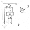
- a microelectronics element embodied as an optical receiver element 1 according to the present invention is shown.
- This embodiment basically corresponds to the example in Fig. 1 , with the optical receiver element 1 comprising a functional unit 2, this time in the form of a photosensor comprising a photodiode.
- the optical receiver element 1 further comprises a rectifier 3, and both the photodiode 2 and the rectifier 3 are integrated on a common semiconductor substrate 4.
- the rectifier can have a variety of different forms (e.g. a diode bridge-type rectifier, a voltage-adjusting rectifier, etc.) and may comprise an active rectifier circuit or a passive rectifier circuit.
- silicon, germanium or any other suitable material may be again used.
- the proper choice of the semiconductor material will usually depend upon the desired range of the wavelengths of the light to be detected by the photodiode 2. For wavelengths of up to 1.1 micrometer, for example, silicon is usually a more suitable material, whereas for wavelengths of up to 1.8 micrometer germanium may be used.
- the optical receiver element 1 is driven by an AC voltage U AC .
- the frequency of the AC voltage lies between 100 kHz to 100 MHz.
- the AC voltage U AC is applied to the voltage supply pins 5 and 6.
- the rectifier 3 is adapted for converting the AC voltage into a DC voltage U DC .
- the rectifier 3 is composed of one or more diodes and may comprise one or more filter capacitors or buffer capacitors for generating a smoothed DC voltage U DC . This DC voltage then forms a supply voltage for the photodiode 2.
- the photodiode 2 is used in the so-called "photoconductive mode" under reverse bias.
- Photodiodes which are operated in the photoconductive mode are more sensitive to light than the ones based upon the photovoltaic effect and also tend to have lower capacitance, which improves the speed of their time response.
- a further effect of the reverse bias is widening of the depletion layer and strengthening of the photocurrent.
- the optical receiver element 1 in this embodiment of the invention also comprises a capacitor 8 connected to a terminal 9 of the photodiode 2, with the capacitor 8 adapted for uncoupling or decoupling an output signal 10 from the photodiode circuit.
- the output signal 10 solely comprises the alternating component of the received signal.
- the modulation of the modulated light 7 may, for example, be chosen such that the output signal 10 does not comprise any constant component, or only a negligible constant component.
- the output signal 10 is supplied to an output pin 11 of the optical receiver element 1.
- the optical receiver element 1 comprises a photosensitive area 15 that is made of a material that is transparent for the light to be detected.
- the voltage supply pins 5, 6 and the output pin 11 are located at a reverse side of the packaged element 1 opposite to the photosensitive area 15.
- the optical receiver element 1 shown in Fig. 2 and Fig. 3 is especially well-suited for realizing optical data transmission in a surrounding where electrochemical corrosion is likely to occur.
- the optical receiver element 1 is designed to be operated with AC voltage instead of DC voltage.
- Photodiodes that have been used to date have required a DC voltage supply, and this has often led to galvanic corrosion of the metal elements exposed to the aqueous environment in the body.
- the DC voltage supply is replaced by an AC voltage supply, so that damage resulting from galvanic corrosion may be significantly reduced or completely avoided. This allows use of optical data transmission in aqueous environments where galvanic corrosion was previously a problem.
- optical data transmission via modulated light offers numerous advantages. Firstly, optical data transmission is characterized by its resistance to interference. Further, the design of the transmitter and receiver elements is comparatively simple, and the amount of energy consumed by an optical receiver element is quite low. The area required to accommodate an optical receiver element is also relatively small.
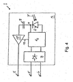
- the optical receiver element 1 comprises a functional unit 2, again in the form of a photosensor comprising a photodiode, in combination with a rectifier 3, a capacitor 8, an ambient light control circuit 16, and an amplifier 17. All of these components are integrated on one common semiconductor substrate 4. Compared to the embodiment shown in Fig. 2 of the drawings, therefore, the ambient light control circuit 16 and the amplifier 17 have been added.
- an AC supply voltage U AC is applied to the two voltage supply pins 5, 6.
- the rectifier 3 is adapted for converting the AC supply voltage U AC to a DC voltage U DC , with U DC then forming, or being used as, a supply voltage for the ambient light control circuit 16 and the amplifier 17.
- the ambient light control circuit 16 determines the intensity of the ambient light. Dependent upon the intensity of the ambient light, the ambient light control circuit 16 supplies an operating voltage to the photodiode 2, whereby the operating point of the photodiode 2 is set to a respective optimum.
- modulated light 7 strikes the photodiode 2
- a modulated photocurrent is generated.
- the alternating component of the photocurrent is uncoupled or decoupled by the capacitor 8 and supplied to the amplifier 17.
- the ambient light control circuit 16 may comprise an automatic gain control.
- the automatic gain control is adapted for controlling the gain of the amplifier 17 in dependence upon the amplitude of the modulated detection signal, and for providing a gain control signal 18 to the amplifier 17.
- the amplifier's input signal is amplified according to the gain control signal 18, and the amplifier's output signal is provided to the output pin 11 of the optical receiver element 1.
- amplification of the modulated detection signal is activated as soon as the ambient light intensity exceeds a predefined threshold.
- the amplifier 16 has a logarithmic characteristic.
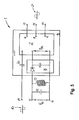
- a microelectronics element in the form of a microchip 1 illustrating another example of the invention is shown.
- the microchip 1 is again designed to be implanted in the human or animal body in a medical implant device and again comprises application specific microelectronics in a functional unit 2 for performing a function in the medical implant device, and rectifier means 3 adapted for converting an AC supply voltage into a DC voltage.
- the rectifier means 3 comprises at least one diode and may include one or more filter capacitor or buffer capacitor for generating a smoothed DC voltage.
- the rectifier means 3 may again take a variety of different forms (e.g.
- both the functional unit 2 and the rectifier means 3 are again integrated on a common semiconductor substrate 4, with the arrangement of the rectifier means 3 and the associated circuitry configured to form a corrosion suppression means with which the microelectronics element, i.e. the microchip 1, avoids or is isolated from an externally applied or acting DC signal or DC supply voltage.
- the microchip 1 in Fig. 5 is adapted to be driven by an AC voltage supply U AC which is applied to voltage supply pins 5 and 6.
- the rectifier means 3 is adapted to convert the AC voltage supply U AC applied to the voltage supply pins 5 and 6 into a DC voltage U DC and this DC voltage is then used to supply voltage to the application specific microelectronics of the functional unit 2.
- the microchip 1 in the present example comprises an input pin 19 for receiving a signal 10 to be processed.
- This signal 10 may, for example, be the output signal of an optical receiver element 1 according to one the embodiments of Figs. 1 to 4 .
- the capacitor 20 shown in the input line extending from the input terminal 19 is optional and may be included to filter or tune the signal 10.
- the functional unit 2 of the microchip 1 may comprise a processor adapted for processing the output signal 10 from an optical receiver element.
- the microchip 1 of Fig. 5 may be adapted for processing the signal 10 in the processor unit 2 and then transmitting stimulation signals 21 to the plurality of electrodes of a retina-stimulating electrode array in the retinal implant via a plurality of output pins 11 of the microchip 1.
- a retinal implant device for implantation in a patient's eye is shown.
- Light passing through the cornea 29 and the eye lens 30 strikes the retina 31, which covers a large part of the eyeball's interior, primarily at the inner surface of the rear or posterior wall of the eye.
- the eyeball's outer surface is formed by the sclera 32.
- a choroid membrane 33 is located between the retina 31 and the sclera 32.
- the iris 34 determines the size of the pupil and, thus, the amount of light that may enter into the interior of the eye.
- the eye lens 30 is fixed by the ciliary muscle 35 or is explanted.
- the implant device comprises an intraocular part 36 and an extra-ocular part 37.
- the intraocular part 36 is located in the interior of the eye, whereas the extraocular part 37 is fixed to the outer surface of the sclera 32.
- the intraocular part 36 and the extraocular part 37 are electrically connected by a wire connection 38 that passes through the sclera 32 at a position directly behind the ciliary muscle 35.
- a retinal implant device is a visual prosthesis designed to provide some degree of visual perception to patients suffering from retinal degenerative diseases such as retinitis pigmentosa or macula degeneration.
- the apparatus includes an eye glasses 42 to be worn by the patient, the eye glasses 42 having a small video camera 40 integrated in or on the glasses frame 39.
- a video signal acquired by the video camera 40 is processed, and the image data are transmitted to the retinal implant device 43 via a modulated infrared light beam 41.
- the infrared beam 41 may, for example, be generated by an infrared transmitter LED (not shown) located on or in the vicinity of the glasses 42.
- the modulated infrared beam 41 passes through the patient's eye, including through the lens 30 of the eye, if still present, or otherwise through the space normally occupied by the lens 30, and strikes an optical receiver element 1 of the invention incorporated in the implant device 43.
- a microelectronics element in the form of an optical receiver element 1 of the kind described with reference to drawing Figs. 3 to 5 may be employed, driven by an AC supply voltage.
- an AC supply voltage For a retinal implant, long-term stability is an important issue. Therefore, it is important to avoid galvanic corrosion of the wire connections and voltage supply lines.
- galvanic corrosion By supplying an AC supply voltage to the optical receiver element 1, galvanic corrosion can be either eliminated or at least significantly reduced.
- the image data received by the optical receiver element 1 is forwarded via the wire connection 38 to a retina stimulation chip 44.
- the retina stimulation chip 44 is operative to convert the image data into a sequence of stimulation pulses.
- the retinal stimulation chip 44 is implemented as a digital signal processing chip and may also constitute an embodiment of the present invention. That is, the retinal stimulation chip 44 may comprise a microchip incorporating the concept described above with reference to drawing Fig. 5 , in which the functional unit comprises a processor circuit.
- the stimulation pulses are supplied to an array of micro-contacts located on the intraocular part 36, namely on the retinal implant 43 implanted directly on the retina 31.
- the micro-contacts are adapted for stimulating the ganglia cells of the retina 31.
- the electrical power required for operating the retinal implant in particular the electrical power consumed by the optical receiver element 1 and/or the retina stimulation chip 44, can be provided by a high frequency transmitter coil 46 that is inductively coupled with a high frequency receiver coil 47 located on the extra-ocular part 37 of the retina implant.
- the AC voltage provided by such a high frequency receiver coil 47 may thus used for powering either or both of the optical receiver element 1 and the retina stimulation chip 44.
Landscapes
- Health & Medical Sciences (AREA)
- Life Sciences & Earth Sciences (AREA)
- Engineering & Computer Science (AREA)
- Biomedical Technology (AREA)
- Nuclear Medicine, Radiotherapy & Molecular Imaging (AREA)
- Radiology & Medical Imaging (AREA)
- Animal Behavior & Ethology (AREA)
- General Health & Medical Sciences (AREA)
- Public Health (AREA)
- Veterinary Medicine (AREA)
- Neurology (AREA)
- Neurosurgery (AREA)
- Ophthalmology & Optometry (AREA)
- Prostheses (AREA)
Description
- The present invention relates to a medical implant device, and more particularly to a microelectronics element, such as a microchip, to be incorporated in the medical implant device.
- In a particularly preferred application of the present invention, the medical implant device comprises a retinal implant and the microelectronics element may be in the form of an optical receiver element for the retinal implant. It will be appreciated, however, that the present invention is not limited to this particular application, but may be employed in various medical implant applications where microelectronic components are used, including, for example, pacemakers, cochlea implants and hearing aids, neural implants, as well as other implant devices.
- When microelectronic components are employed in medical implant devices, an important consideration is to protect the microelectronic components from the adverse affects of the aqueous environment usually encountered within the human or animal body. In particular, the moisture or fluids of the human or animal body to which such medical implant devices are almost invariably exposed are typically electrolytic conductors and create a potentially corrosive environment for the microelectronic components, especially when those components are supplied with a direct current (DC) voltage via a battery power source or a converted alternating current (AC) power supply. When the microelectronic components are exposed to corrosive influences, the efficacy of the medical implant device can be compromised leading to reduced performance or even to a complete failure of the device. For example, when an optical receiver element is used in an environment where it is exposed to aqueous solutions or other liquids, proper functioning of the receiver element may be impaired by electrochemical corrosion.
- A typical solution to this problem is to enclose or encase the microelectronics and other sensitive components in such a way that they are impervious to moisture. For example, the sensitive components or even the entire medical implant device may be hermetically sealed from the aqueous environment of the body, for example, by an enclosure or a coating layer, such as a polymer coating. Silicone polymers are particularly favorable in this context because of their high bio-compatibility. Such a coating layer, however, not only complicates the manufacturing process, but also has the problem that the microelectronic components still need to maintain an electrical contact with external components. This often requires that a physical connection be provided through the protective enclosure or coating layer and, thus, a breach in the protective enclosure or layer is created. Additionally, while sealing some components or the entire implant device with, for example, a polymer coating layer can provide effective protection from a corrosive environment, it can also involve a conflict between the requirements of impermeability to moisture on the one hand; and flexibility of the implant device on the other, particularly in the field of retinal implants.
-
EP 0 247 649 A (COMMW OF AUSTRALIA [AU]) (1987-12-02) discloses a cochlear implant where corrosion through DC current is considered andUS 2007/142877 A1 (MCLEAN GEORGE Y [US]) (2007-06-21 ) considers a retinal implant with rectifying means for converting the AC current into DC current. - It is therefore an object of the present invention to provide a medical implant device in which the sensitive microelectronic components of the device are adequately protected from the aqueous environment of the human or animal body, without all of the drawbacks or limitations noted above.
- The present invention provides a microelectronics element for a medical implant device as defined in
claim 1. Furthermore, the invention provides a medical implant device, such as a retinal implant; as defined in claim 12. Preferred features of the invention are recited in the dependent claims. - In one broad aspect, therefore, the present invention provides a microelectronics element, such as a microchip, for a medical implant device to be implanted in the human or animal body, the microelectronics element comprising: a functional unit including application specific microelectronics for performing a function in the medical implant device, and rectifier means adapted for converting an alternating current (AC) supply voltage into a direct current (DC) voltage. The DC voltage provided by the rectifier means, or an operating voltage which is derived from the DC voltage, is configured to_be supplied to the functional unit. The functional unit and the rectifier means are integrated on a common semiconductor substrate such that the microelectronics element does not need an external DC voltage supply. In other words, the microelectronics element of the invention is configured to avoid, or to be isolated from, application of a DC signal; for example, there is no DC signal at an outer region of the microelectronics element (i.e. microchip) that forms an interface with an aqueous environment in the human or animal body.
- Thus, the present invention provides corrosion suppression means adapted to isolate a microelectronics element or a microchip from the adverse affects of an externally applied or acting DC voltage. In particular, the configuration of the microelectronics element or microchip of the invention renders it designed for exposure to an AC supply voltage only, and desirably excludes the flow of direct current outside of, out from, and/or at a body-interface of the element or microchip of the invention. This, in turn, renders the microelectronics element or microchip inherently resistant to the corrosive effects of the aqueous environment within the body. In particular, the external application of an AC supply voltage to the microelectronics element or microchip of the invention does not give rise to the same corrosive effects experienced with DC voltage supply due to the constantly (and frequently) alternating polarity of the voltage supply. The integration of the rectifier means with the application specific microelectronics of the functional unit on one common semiconductor substrate, e.g. in a microchip, in such a manner that the rectifier means isolates the microelectronics element from an externally applied or acting DC voltage thus forms a corrosion suppression means in the microelectronics element. While a polymer coating layer may still be desirably employed with such an element, lower thicknesses of the coating layer providing greater flexibility are more viable.
- In a preferred form of the invention, the microelectronics element further comprises a capacitor integrated on the common substrate and connected to a terminal of said functional unit, such that the capacitor is adapted for decoupling an alternating component of a signal output from the functional unit. In particular, the decoupling capacitor may be arranged to ensure that a signal output from the microelectronics element or microchip (e.g. at an output pin) only has an alternating component. This capacitor arrangement can therefore again serve to exclude the direct action of an external DC signal on an outside of the microelectronics element or microchip (i.e. at an interface with an aqueous environment of the body); that is, it may serve to avoid direct exposure of the microelectronics element or microchip of the invention to an external DC signal.
- In a preferred form of the invention, the microelectronics element further comprises an amplifier adapted to amplify a signal which is output from the functional unit, or a signal which is derived therefrom.
- In one particular form of the invention, the application specific microelectronics of the functional unit may comprise a processor, such as a data processor.
- In a more preferred form of the invention, however, the functional unit consists of, or comprises, a photosensor which is adapted for detecting incident light, such that the microelectronics element can be embodied as an optical receiver element. The photosensor may, for example, be adapted for converting a modulated light signal into a corresponding detection signal. In this connection, the photosensor may be adapted to receive and detect a light signal, and more preferably, an infrared light signal. The photosensor may, for example, be in the form of a photodiode.
- In a particularly preferred embodiment, therefore, the invention provides an optical receiver element comprising: a photosensor adapted for detecting incident light, and a rectifier adapted for converting an AC supply voltage into a DC voltage. The DC voltage from the rectifier, or an operating voltage derived from the DC voltage, is supplied to the photosensor, and the rectifier and the photosensor are integrated on one common semiconductor substrate.
- By integrating the rectifier and the photodiode on one common substrate, the optical receiver element is adapted to be operated with AC voltage instead of DC voltage. Photodiodes used previously have typically required a DC voltage supply, which has often led to the galvanic corrosion of metal elements that are exposed to an aqueous environment. In the optical receiver element according to embodiments of the present invention, the DC voltage supply is replaced by an AC voltage supply. Thus, the DC voltage generated by the rectifier does not come into direct contact with the medium external to the optical receiver element. With regard to the AC supply voltage, the problems related to galvanic corrosion are much less severe, because the polarity of the supply lines changes at high frequency. By employing an AC voltage as a supply voltage, therefore, damage due to galvanic corrosion may be significantly reduced or even completely avoided. This invention thus supports the use of optical data transmission in environments where galvanic corrosion is likely to occur.
- Optical data transmission via modulated light, preferably in the infrared spectrum, offers a multitude of advantages. Optical data transmission is characterized by its resistance to interference. The design of the transmitter and the receiver element is comparatively simple. Furthermore, the amount of energy consumed by the optical receiver element is quite low, and the area needed for accommodating an optical receiver element is relatively small.
- In another broad aspect, the invention provides a microelectronics element, such as a microchip, for a medical implant device to be implanted in the human or animal body, the microelectronics element comprising: a functional unit including application specific microelectronics for performing a function in the medical implant device, rectifier means adapted for converting an AC supply voltage into a DC voltage, and corrosion suppression means for inhibiting electrolytic corrosion of the microelectronics element in an aqueous environment. The DC voltage provided by the rectifier means, or an operating voltage which is derived from the DC voltage, is configured to be supplied to the functional unit. The corrosion suppression means comprises a circuit configuration in which the functional unit and the rectifier means are integrated on a common semiconductor substrate such that the microelectronics element avoids the presence of an external DC signal being (directly) applied to and/or acting (directly) on the microelectronics element.
- In this way, even where a physical electrical connection extends through a thin coating layer in the microelectronics element or microchip of the invention, the isolation of the element or microchip from a DC signal by the corrosion suppression means results in the desired inhibition of any corrosive effects. That is, the microelectronics element or microchip of the invention is not exposed to direct current in the corrosive aqueous environment.
- A medical implant according to an embodiment of the present invention comprises a microelectronics element, preferably in the form of an optical receiver element, as described above. The medical implant is desirably a retinal implant, with the optical receiver element being adapted for receiving and detecting a modulated light signal.
- The microelectronics element of the invention is especially well-suited for use in a medical implant device that is exposed to all kinds of body fluids. For a medical implant, long-term stability is highly important, because replacement of an implant device typically requires surgery. By using a microelectronics element according to an embodiment of the present invention, electrochemical corrosion is significantly reduced or even completely eliminated, and hence, the lifetime of the medical implant device is prolonged. By using an AC supply voltage for microelectronics elements (e.g. optical receiver elements) that have to date generally been supplied by a DC voltage, the long-term stability of the medical implant device is improved.
- The above and further features and advantages of the present invention will become more apparent from the following detailed description of preferred embodiments of the invention with reference to the accompanying drawings, in which like reference numerals identify like parts, and in which:
- Fig. 1
- shows a microelectronics element illustrating an example of the concept of the present invention;
- Fig. 2
- shows an optical receiver element according to an embodiment of the present invention;
- Fig. 3
- shows the packaging of an optical receiver element according to an embodiment of the present invention;
- Fig. 4
- shows an optical receiver element according to another embodiment of the present invention;
- Fig. 5
- shows a microelectronics element illustrating another example of the concept of the present invention; and
- Fig. 6
- shows a retinal implant device comprising an optical receiver element according to an embodiment of the present invention.
- Referring firstly to
Fig. 1 of the drawings, a microelectronics element in the form of amicrochip 1 illustrating an example of the invention is shown. Themicrochip 1 is designed to be implanted in the human or animal body in a medical implant device and comprises application specific microelectronics in afunctional unit 2 for performing a function in the medical implant device, and rectifier means 3 adapted for converting an AC supply voltage into a DC voltage. In this example, the rectifier means 3 comprises at least one diode and may include one or more filter capacitor or buffer capacitor for generating a smoothed DC voltage. It will be appreciated, however, that the rectifier means 3 may take a variety of different forms (e.g. a diode bridge-type rectifier, a voltage-adjusting rectifier, etc.) and may comprise an active rectifier circuit or a passive rectifier circuit. - Both the
functional unit 2 and the rectifier means 3 are integrated on a common semiconductor substrate 4 (formed, for example, from silicon, germanium or any other suitable material), with the arrangement of the rectifier means 3 and the associated circuitry configured to form corrosion suppression means with which the microelectronics element, i.e. themicrochip 1, avoids any externally applied or acting DC signal or DC supply voltage. In other words, themicrochip 1 is adapted to be driven by an AC voltage supply UAC which is applied tovoltage supply pins 5 and 6. The frequency of the AC voltage preferably lies in the range of about 100 kHz to 100 MHz. The rectifier means 3 is adapted to convert the AC voltage supply UAC applied to thevoltage supply pins 5 and 6 into a DC voltage UDC and this DC voltage then forms a supply voltage for the application specific microelectronics of thefunctional unit 2, i.e. at one or more input terminal of thefunctional unit 2. Themicrochip 1 further comprises acapacitor 8, which is connected to anoutput terminal 9 of thefunctional unit 2. Thecapacitor 8 is adapted for decoupling anoutput signal 10 from thefunctional unit 2, such that anoutput signal 10 at anoutput pin 11 of themicrochip 1 comprises the alternating component of the signal generated by or output from thefunctional unit 2. A tuning arrangement comprising a capacitor 12 and aninductor 13 may optionally be provided in the AC voltage supply circuitry between the supply pins 5, 6. Although not so shown, it will be appreciated that the tuning capacitor 12 and/orinductor 13 could also be integrated on thecommon semiconductor substrate 4. - With reference now to
Fig. 2 of the drawings, a microelectronics element embodied as anoptical receiver element 1 according to the present invention is shown. This embodiment basically corresponds to the example inFig. 1 , with theoptical receiver element 1 comprising afunctional unit 2, this time in the form of a photosensor comprising a photodiode. Theoptical receiver element 1 further comprises a rectifier 3, and both thephotodiode 2 and the rectifier 3 are integrated on acommon semiconductor substrate 4. As before, the rectifier can have a variety of different forms (e.g. a diode bridge-type rectifier, a voltage-adjusting rectifier, etc.) and may comprise an active rectifier circuit or a passive rectifier circuit. Also, as the semiconductor material, silicon, germanium or any other suitable material may be again used. In this case, however, the proper choice of the semiconductor material will usually depend upon the desired range of the wavelengths of the light to be detected by thephotodiode 2. For wavelengths of up to 1.1 micrometer, for example, silicon is usually a more suitable material, whereas for wavelengths of up to 1.8 micrometer germanium may be used. - The
optical receiver element 1 is driven by an AC voltage UAC. Preferably, the frequency of the AC voltage lies between 100 kHz to 100 MHz. The AC voltage UAC is applied to thevoltage supply pins 5 and 6. The rectifier 3 is adapted for converting the AC voltage into a DC voltage UDC. The rectifier 3 is composed of one or more diodes and may comprise one or more filter capacitors or buffer capacitors for generating a smoothed DC voltage UDC. This DC voltage then forms a supply voltage for thephotodiode 2. Thephotodiode 2 is used in the so-called "photoconductive mode" under reverse bias. Photodiodes which are operated in the photoconductive mode are more sensitive to light than the ones based upon the photovoltaic effect and also tend to have lower capacitance, which improves the speed of their time response. A further effect of the reverse bias is widening of the depletion layer and strengthening of the photocurrent. - When a beam of modulated light 7 is incident on the
photodiode 2, a photocurrent is generated that alternates in accordance with the modulation of the modulated light 7. Theoptical receiver element 1 in this embodiment of the invention also comprises acapacitor 8 connected to aterminal 9 of thephotodiode 2, with thecapacitor 8 adapted for uncoupling or decoupling anoutput signal 10 from the photodiode circuit. Theoutput signal 10 solely comprises the alternating component of the received signal. The modulation of the modulated light 7 may, for example, be chosen such that theoutput signal 10 does not comprise any constant component, or only a negligible constant component. Theoutput signal 10 is supplied to anoutput pin 11 of theoptical receiver element 1. -
Fig. 3 of the drawings schematically illustrates the external design of theoptical receiver element 1. In this regard, theoptical receiver element 1 comprises aphotosensitive area 15 that is made of a material that is transparent for the light to be detected. Preferably, thevoltage supply pins 5, 6 and theoutput pin 11 are located at a reverse side of the packagedelement 1 opposite to thephotosensitive area 15. - The
optical receiver element 1 shown inFig. 2 and Fig. 3 is especially well-suited for realizing optical data transmission in a surrounding where electrochemical corrosion is likely to occur. By integrating thephotodiode 2 and the rectifier 3 on onecommon substrate 4, theoptical receiver element 1 is designed to be operated with AC voltage instead of DC voltage. Photodiodes that have been used to date have required a DC voltage supply, and this has often led to galvanic corrosion of the metal elements exposed to the aqueous environment in the body. In theoptical receiver element 1 according to the present invention, however, the DC voltage supply is replaced by an AC voltage supply, so that damage resulting from galvanic corrosion may be significantly reduced or completely avoided. This allows use of optical data transmission in aqueous environments where galvanic corrosion was previously a problem. - As noted above, optical data transmission via modulated light, preferably in the infrared spectrum, offers numerous advantages. Firstly, optical data transmission is characterized by its resistance to interference. Further, the design of the transmitter and receiver elements is comparatively simple, and the amount of energy consumed by an optical receiver element is quite low. The area required to accommodate an optical receiver element is also relatively small.
- In
Fig. 4 of the drawings another embodiment of anoptical receiver element 1 according to the present invention is depicted. In this example, theoptical receiver element 1 comprises afunctional unit 2, again in the form of a photosensor comprising a photodiode, in combination with a rectifier 3, acapacitor 8, an ambientlight control circuit 16, and anamplifier 17. All of these components are integrated on onecommon semiconductor substrate 4. Compared to the embodiment shown inFig. 2 of the drawings, therefore, the ambientlight control circuit 16 and theamplifier 17 have been added. - Again, an AC supply voltage UAC is applied to the two
voltage supply pins 5, 6. The rectifier 3 is adapted for converting the AC supply voltage UAC to a DC voltage UDC, with UDC then forming, or being used as, a supply voltage for the ambientlight control circuit 16 and theamplifier 17. The ambientlight control circuit 16 determines the intensity of the ambient light. Dependent upon the intensity of the ambient light, the ambientlight control circuit 16 supplies an operating voltage to thephotodiode 2, whereby the operating point of thephotodiode 2 is set to a respective optimum. When modulated light 7 strikes thephotodiode 2, a modulated photocurrent is generated. The alternating component of the photocurrent is uncoupled or decoupled by thecapacitor 8 and supplied to theamplifier 17. - The ambient
light control circuit 16 may comprise an automatic gain control. The automatic gain control is adapted for controlling the gain of theamplifier 17 in dependence upon the amplitude of the modulated detection signal, and for providing again control signal 18 to theamplifier 17. The amplifier's input signal is amplified according to thegain control signal 18, and the amplifier's output signal is provided to theoutput pin 11 of theoptical receiver element 1. According to a preferred embodiment of the invention, amplification of the modulated detection signal is activated as soon as the ambient light intensity exceeds a predefined threshold. According to a further preferred embodiment, theamplifier 16 has a logarithmic characteristic. - With reference now to
Fig. 5 of the drawings, a microelectronics element in the form of amicrochip 1 illustrating another example of the invention is shown. Themicrochip 1 is again designed to be implanted in the human or animal body in a medical implant device and again comprises application specific microelectronics in afunctional unit 2 for performing a function in the medical implant device, and rectifier means 3 adapted for converting an AC supply voltage into a DC voltage. As before, the rectifier means 3 comprises at least one diode and may include one or more filter capacitor or buffer capacitor for generating a smoothed DC voltage. In other words, the rectifier means 3 may again take a variety of different forms (e.g. a diode bridge-type rectifier, a voltage-adjusting rectifier, etc.) and may comprise an active rectifier circuit or a passive rectifier circuit. Importantly, both thefunctional unit 2 and the rectifier means 3 are again integrated on acommon semiconductor substrate 4, with the arrangement of the rectifier means 3 and the associated circuitry configured to form a corrosion suppression means with which the microelectronics element, i.e. themicrochip 1, avoids or is isolated from an externally applied or acting DC signal or DC supply voltage. - Thus, the
microchip 1 inFig. 5 is adapted to be driven by an AC voltage supply UAC which is applied tovoltage supply pins 5 and 6. The rectifier means 3 is adapted to convert the AC voltage supply UAC applied to thevoltage supply pins 5 and 6 into a DC voltage UDC and this DC voltage is then used to supply voltage to the application specific microelectronics of thefunctional unit 2. In contrast to the embodiments ofFigs. 1 to 4 , however, in which an input interface of the microchip 1 (not illustrated in those cases) was, for example, adapted for optical data transfer, themicrochip 1 in the present example comprises aninput pin 19 for receiving asignal 10 to be processed. Thissignal 10 may, for example, be the output signal of anoptical receiver element 1 according to one the embodiments ofFigs. 1 to 4 . Thecapacitor 20 shown in the input line extending from theinput terminal 19 is optional and may be included to filter or tune thesignal 10. - In this case, therefore, the
functional unit 2 of themicrochip 1 may comprise a processor adapted for processing theoutput signal 10 from an optical receiver element. Thus, when employed in a retinal implant device, as will be described in more detail below, themicrochip 1 ofFig. 5 may be adapted for processing thesignal 10 in theprocessor unit 2 and then transmitting stimulation signals 21 to the plurality of electrodes of a retina-stimulating electrode array in the retinal implant via a plurality of output pins 11 of themicrochip 1. - With reference now to
Fig. 6 of the drawings, a retinal implant device for implantation in a patient's eye is shown. Light passing through thecornea 29 and the eye lens 30 (which may or may not be present in the patient to be treated) strikes theretina 31, which covers a large part of the eyeball's interior, primarily at the inner surface of the rear or posterior wall of the eye. The eyeball's outer surface is formed by thesclera 32. Achoroid membrane 33 is located between theretina 31 and thesclera 32. Theiris 34 determines the size of the pupil and, thus, the amount of light that may enter into the interior of the eye. The eye lens 30 is fixed by theciliary muscle 35 or is explanted. The implant device comprises anintraocular part 36 and an extra-ocular part 37. Theintraocular part 36 is located in the interior of the eye, whereas the extraocular part 37 is fixed to the outer surface of thesclera 32. Theintraocular part 36 and the extraocular part 37 are electrically connected by awire connection 38 that passes through the sclera 32 at a position directly behind theciliary muscle 35. - A retinal implant device is a visual prosthesis designed to provide some degree of visual perception to patients suffering from retinal degenerative diseases such as retinitis pigmentosa or macula degeneration. To this end, the apparatus includes an
eye glasses 42 to be worn by the patient, theeye glasses 42 having asmall video camera 40 integrated in or on theglasses frame 39. A video signal acquired by thevideo camera 40 is processed, and the image data are transmitted to theretinal implant device 43 via a modulatedinfrared light beam 41. Theinfrared beam 41 may, for example, be generated by an infrared transmitter LED (not shown) located on or in the vicinity of theglasses 42. The modulatedinfrared beam 41 passes through the patient's eye, including through the lens 30 of the eye, if still present, or otherwise through the space normally occupied by the lens 30, and strikes anoptical receiver element 1 of the invention incorporated in theimplant device 43. - According to embodiments of the present invention, a microelectronics element in the form of an
optical receiver element 1 of the kind described with reference to drawingFigs. 3 to 5 may be employed, driven by an AC supply voltage. For a retinal implant, long-term stability is an important issue. Therefore, it is important to avoid galvanic corrosion of the wire connections and voltage supply lines. By supplying an AC supply voltage to theoptical receiver element 1, galvanic corrosion can be either eliminated or at least significantly reduced. - The image data received by the
optical receiver element 1 is forwarded via thewire connection 38 to aretina stimulation chip 44. Theretina stimulation chip 44 is operative to convert the image data into a sequence of stimulation pulses. Preferably, theretinal stimulation chip 44 is implemented as a digital signal processing chip and may also constitute an embodiment of the present invention. That is, theretinal stimulation chip 44 may comprise a microchip incorporating the concept described above with reference to drawingFig. 5 , in which the functional unit comprises a processor circuit. Via thewire connection 38, the stimulation pulses are supplied to an array of micro-contacts located on theintraocular part 36, namely on theretinal implant 43 implanted directly on theretina 31. The micro-contacts are adapted for stimulating the ganglia cells of theretina 31. - The electrical power required for operating the retinal implant, in particular the electrical power consumed by the
optical receiver element 1 and/or theretina stimulation chip 44, can be provided by a highfrequency transmitter coil 46 that is inductively coupled with a high frequency receiver coil 47 located on the extra-ocular part 37 of the retina implant. The AC voltage provided by such a high frequency receiver coil 47 may thus used for powering either or both of theoptical receiver element 1 and theretina stimulation chip 44.
Claims (15)
- A microelectronics element (1) for a medical implant device to be implanted in the human or animal body, the microelectronics element (1) comprising:a functional unit (2) including application specific microelectronics for performing a function in the medical implant device, the functional unit (2) comprising a photosensor for detecting incident light;rectifier means (3) adapted for converting an AC supply voltage into a DC voltage, wherein the DC voltage provided by the rectifier means (3), or an operating voltage derived from the DC voltage, is adapted to be supplied to the functional unit (2);wherein the functional unit (2) and the rectifier means (3) are integrated on a common semiconductor substrate (4) such that the micro-electronics element (1) is isolated from direct application and/or action of an external DC signal to suppress corrosion in an aqueous environment.
- A microelectronics element (1) according to claim 1, wherein the micro-electronics element (1) is adapted to function as an optical receiver element.
- A microelectronics element (1) according to claim 1 or claim 2, further comprising a capacitor (8) integrated on the common substrate (4) and connected to a terminal of said functional unit (2), wherein the capacitor (8) is adapted for decoupling an alternating component of a signal from the functional unit (2).
- A microelectronics element (1) according to any one of the preceding claims, wherein the photosensor is adapted for converting a modulated light signal into a corresponding detection signal.
- A microelectronics element (1) according to any one of the preceding claims, wherein the photosensor is adapted for receiving and detecting an infrared light signal.
- A microelectronics element (1) according to any one of the preceding claims, wherein the photosensor is a photodiode.
- A microelectronics element (1) according to any one of the preceding claims, further comprising an ambient light control circuit (16) integrated on the common substrate (4) and adapted for determining an ambient light intensity.
- A microelectronics element (1) according to claim 7, wherein the ambient light control circuit (16) is adapted for controlling operation of the photosensor in dependence on the determined ambient light intensity.
- A microelectronics element (1) according to any one of the preceding claims, further comprising an amplifier (17) integrated on the common substrate (4) and adapted for amplifying a signal output from the functional unit (2), such as a detection signal detected by the photosensor, or a signal derived therefrom.
- A microelectronics element (1) according to claim 9, wherein the ambient light control circuit (16) comprises an automatic gain control adapted for controlling the amplifier's gain in dependence on the amplitude of the detection signal or the signal derived therefrom.
- A microelectronics element (1) according to claim 10, wherein the ambient light control circuit (16) is adapted for activating amplification of the detection signal, or of the signal derived therefrom, when the ambient light intensity exceeds a predefined threshold.
- A medical implant device to be implanted in the human or animal body, comprising a microelectronics element (1) according to any one of claims 1 to 11.
- A medical implant device according to claim 12, wherein the implant device comprises a retinal implant (43) and the microelectronics element (1) is an optical receiver element (1).
- A medical implant device according to claim 13, wherein the optical receiver element (1) is adapted for receiving a modulated light signal carrying image information and for converting the modulated light signal into a corresponding detection signal; and/or wherein the optical receiver element (1) is adapted for receiving and detecting a modulated infrared signal.
- An implant device according to claim 13 or claim 14, further comprising:an array of micro-contacts to be located on the retina, the micro-contacts being adapted for electrically contacting ganglia of the retina tissue; and/ora retina stimulation chip adapted for converting image information into corresponding stimulation impulses for the array of micro-contacts; and/ora high frequency receiver coil adapted for receiving a high frequency signal and for supplying an AC supply voltage to the microelectronics element (1) and to the retina stimulation chip.
Priority Applications (2)
| Application Number | Priority Date | Filing Date | Title |
|---|---|---|---|
| PL09702331T PL2229212T3 (en) | 2008-01-14 | 2009-01-14 | Retina implant with rectified AC powered photodiode |
| EP09702331.1A EP2229212B1 (en) | 2008-01-14 | 2009-01-14 | Retina implant with rectified AC powered photodiode |
Applications Claiming Priority (3)
| Application Number | Priority Date | Filing Date | Title |
|---|---|---|---|
| EP2008000231 | 2008-01-14 | ||
| PCT/EP2009/000176 WO2009090047A1 (en) | 2008-01-14 | 2009-01-14 | Retinal implant with rectified ac powered photodiode |
| EP09702331.1A EP2229212B1 (en) | 2008-01-14 | 2009-01-14 | Retina implant with rectified AC powered photodiode |
Publications (2)
| Publication Number | Publication Date |
|---|---|
| EP2229212A1 EP2229212A1 (en) | 2010-09-22 |
| EP2229212B1 true EP2229212B1 (en) | 2015-04-29 |
Family
ID=42563065
Family Applications (1)
| Application Number | Title | Priority Date | Filing Date |
|---|---|---|---|
| EP09702331.1A Revoked EP2229212B1 (en) | 2008-01-14 | 2009-01-14 | Retina implant with rectified AC powered photodiode |
Country Status (2)
| Country | Link |
|---|---|
| EP (1) | EP2229212B1 (en) |
| PL (1) | PL2229212T3 (en) |
Citations (11)
| Publication number | Priority date | Publication date | Assignee | Title |
|---|---|---|---|---|
| EP0247649A1 (en) | 1983-04-11 | 1987-12-02 | The Commonwealth Of Australia | Cochlear implant prosthesis current switching and power supply |
| US6324429B1 (en) | 1998-05-08 | 2001-11-27 | Massachusetts Eye And Ear Infirmary | Chronically implantable retinal prosthesis |
| US20030158588A1 (en) | 2002-01-17 | 2003-08-21 | Rizzo Joseph F. | Minimally invasive retinal prosthesis |
| WO2005000395A1 (en) | 2003-06-23 | 2005-01-06 | Eberhard-Karls-Universität Tübingen Universitätsklinikum | Active retina implant comprising a plurality of picture elements |
| WO2006116625A2 (en) | 2005-04-28 | 2006-11-02 | California Institute Of Technology | Batch-fabricated flexible intraocular retinal prosthesis systems and methods for manufacturing the same |
| US7146221B2 (en) | 2001-11-16 | 2006-12-05 | The Regents Of The University Of California | Flexible electrode array for artifical vision |
| US7191010B2 (en) | 2001-02-28 | 2007-03-13 | Nidek Co., Ltd. | Built-in-eye eyesight stimulating apparatus |
| US20070142877A1 (en) | 2005-12-20 | 2007-06-21 | Mclean George Y | Charge-integrating retinal prosthesis and method |
| US7242597B2 (en) | 2004-08-04 | 2007-07-10 | Nidek Co., Ltd. | Rectifier circuit and vision regeneration assisting apparatus having the same |
| EP1618922B1 (en) | 2004-07-23 | 2007-09-05 | Nidek Co., Ltd. | Visual restoration aiding device |
| WO2008037362A2 (en) | 2006-09-26 | 2008-04-03 | Retina Implant Ag | Implantable device |
-
2009
- 2009-01-14 PL PL09702331T patent/PL2229212T3/en unknown
- 2009-01-14 EP EP09702331.1A patent/EP2229212B1/en not_active Revoked
Patent Citations (11)
| Publication number | Priority date | Publication date | Assignee | Title |
|---|---|---|---|---|
| EP0247649A1 (en) | 1983-04-11 | 1987-12-02 | The Commonwealth Of Australia | Cochlear implant prosthesis current switching and power supply |
| US6324429B1 (en) | 1998-05-08 | 2001-11-27 | Massachusetts Eye And Ear Infirmary | Chronically implantable retinal prosthesis |
| US7191010B2 (en) | 2001-02-28 | 2007-03-13 | Nidek Co., Ltd. | Built-in-eye eyesight stimulating apparatus |
| US7146221B2 (en) | 2001-11-16 | 2006-12-05 | The Regents Of The University Of California | Flexible electrode array for artifical vision |
| US20030158588A1 (en) | 2002-01-17 | 2003-08-21 | Rizzo Joseph F. | Minimally invasive retinal prosthesis |
| WO2005000395A1 (en) | 2003-06-23 | 2005-01-06 | Eberhard-Karls-Universität Tübingen Universitätsklinikum | Active retina implant comprising a plurality of picture elements |
| EP1618922B1 (en) | 2004-07-23 | 2007-09-05 | Nidek Co., Ltd. | Visual restoration aiding device |
| US7242597B2 (en) | 2004-08-04 | 2007-07-10 | Nidek Co., Ltd. | Rectifier circuit and vision regeneration assisting apparatus having the same |
| WO2006116625A2 (en) | 2005-04-28 | 2006-11-02 | California Institute Of Technology | Batch-fabricated flexible intraocular retinal prosthesis systems and methods for manufacturing the same |
| US20070142877A1 (en) | 2005-12-20 | 2007-06-21 | Mclean George Y | Charge-integrating retinal prosthesis and method |
| WO2008037362A2 (en) | 2006-09-26 | 2008-04-03 | Retina Implant Ag | Implantable device |
Non-Patent Citations (4)
| Title |
|---|
| A. ROTHERMEL ET AL.: "A 1600-pixel Subretinal Chip with DC-free Termi- nals and ±2V Supply Optimized for Long-Term Lifetime and High Stimulation Efficiency", TAGUNGSBAND ISSCC, 4 February 2008 (2008-02-04), XP031390903 |
| A. STETT ET AL., KÜNSTLICHE NETZHÄUTE, March 2006 (2006-03-01), XP055275798 |
| ABSTRACT ZU D7, December 2007 (2007-12-01) |
| GHOVANLOO ET AL.: "Fully Integrated Wideband High-Current Rec- tifiers for Inductively Powered Devices", IEEE JOURNAL OF SOLID- STATE CIRCUITS, vol. 39, no. 1 1, November 2004 (2004-11-01) |
Also Published As
| Publication number | Publication date |
|---|---|
| PL2229212T3 (en) | 2015-09-30 |
| EP2229212A1 (en) | 2010-09-22 |
Similar Documents
| Publication | Publication Date | Title |
|---|---|---|
| US9002463B2 (en) | Retinal implant with rectified AC powered photodiode | |
| JP5078996B2 (en) | Embedded system with input and output without DC current | |
| US4628933A (en) | Method and apparatus for visual prosthesis | |
| US8150526B2 (en) | Retinal prosthesis | |
| AU2006330586B2 (en) | Charge-integrating retinal prosthesis and method | |
| US9289325B2 (en) | Extraocular epiretinal implant | |
| AU2010350080B2 (en) | Retinal implant and visual prosthesis incorporating such an implant | |
| US20080147144A1 (en) | Cochlear implant | |
| US20100274319A1 (en) | Current leakage detection for a medical implant | |
| US20180169420A1 (en) | Hermetic housing and electronics package for an implant device | |
| EP2229212A1 (en) | Retinal implant with rectified ac powered photodiode | |
| Lemaire et al. | Feasibility assessment of an optically powered digital retinal prosthesis architecture for retinal ganglion cell stimulation | |
| US20200016403A1 (en) | Implant device with optical interface | |
| AU2001268821B2 (en) | Cochlear implant |
Legal Events
| Date | Code | Title | Description |
|---|---|---|---|
| PUAI | Public reference made under article 153(3) epc to a published international application that has entered the european phase |
Free format text: ORIGINAL CODE: 0009012 |
|
| 17P | Request for examination filed |
Effective date: 20100618 |
|
| AK | Designated contracting states |
Kind code of ref document: A1 Designated state(s): AT BE BG CH CY CZ DE DK EE ES FI FR GB GR HR HU IE IS IT LI LT LU LV MC MK MT NL NO PL PT RO SE SI SK TR |
|
| AX | Request for extension of the european patent |
Extension state: AL BA RS |
|
| DAX | Request for extension of the european patent (deleted) | ||
| RAP1 | Party data changed (applicant data changed or rights of an application transferred) |
Owner name: PIXIUM VISION SA |
|
| GRAP | Despatch of communication of intention to grant a patent |
Free format text: ORIGINAL CODE: EPIDOSNIGR1 |
|
| RIC1 | Information provided on ipc code assigned before grant |
Ipc: H01L 27/144 20060101ALI20141204BHEP Ipc: A61N 1/36 20060101AFI20141204BHEP |
|
| INTG | Intention to grant announced |
Effective date: 20141218 |
|
| GRAS | Grant fee paid |
Free format text: ORIGINAL CODE: EPIDOSNIGR3 |
|
| GRAA | (expected) grant |
Free format text: ORIGINAL CODE: 0009210 |
|
| AK | Designated contracting states |
Kind code of ref document: B1 Designated state(s): AT BE BG CH CY CZ DE DK EE ES FI FR GB GR HR HU IE IS IT LI LT LU LV MC MK MT NL NO PL PT RO SE SI SK TR |
|
| REG | Reference to a national code |
Ref country code: GB Ref legal event code: FG4D |
|
| REG | Reference to a national code |
Ref country code: CH Ref legal event code: EP |
|
| REG | Reference to a national code |
Ref country code: AT Ref legal event code: REF Ref document number: 724103 Country of ref document: AT Kind code of ref document: T Effective date: 20150515 |
|
| REG | Reference to a national code |
Ref country code: IE Ref legal event code: FG4D |
|
| REG | Reference to a national code |
Ref country code: CH Ref legal event code: NV Representative=s name: RIEDERER HASLER AND PARTNER PATENTANWAELTE AG, LI |
|
| REG | Reference to a national code |
Ref country code: DK Ref legal event code: T3 Effective date: 20150602 |
|
| REG | Reference to a national code |
Ref country code: DE Ref legal event code: R096 Ref document number: 602009030944 Country of ref document: DE Effective date: 20150611 |
|
| REG | Reference to a national code |
Ref country code: SE Ref legal event code: TRGR |
|
| REG | Reference to a national code |
Ref country code: NL Ref legal event code: T3 |
|
| REG | Reference to a national code |
Ref country code: PT Ref legal event code: SC4A Free format text: AVAILABILITY OF NATIONAL TRANSLATION Effective date: 20150527 |
|
| REG | Reference to a national code |
Ref country code: ES Ref legal event code: FG2A Ref document number: 2541932 Country of ref document: ES Kind code of ref document: T3 Effective date: 20150728 |
|
| REG | Reference to a national code |
Ref country code: NO Ref legal event code: T2 Effective date: 20150429 |
|
| REG | Reference to a national code |
Ref country code: LT Ref legal event code: MG4D |
|
| REG | Reference to a national code |
Ref country code: PL Ref legal event code: T3 |
|
| PG25 | Lapsed in a contracting state [announced via postgrant information from national office to epo] |
Ref country code: HR Free format text: LAPSE BECAUSE OF FAILURE TO SUBMIT A TRANSLATION OF THE DESCRIPTION OR TO PAY THE FEE WITHIN THE PRESCRIBED TIME-LIMIT Effective date: 20150429 Ref country code: LT Free format text: LAPSE BECAUSE OF FAILURE TO SUBMIT A TRANSLATION OF THE DESCRIPTION OR TO PAY THE FEE WITHIN THE PRESCRIBED TIME-LIMIT Effective date: 20150429 Ref country code: FI Free format text: LAPSE BECAUSE OF FAILURE TO SUBMIT A TRANSLATION OF THE DESCRIPTION OR TO PAY THE FEE WITHIN THE PRESCRIBED TIME-LIMIT Effective date: 20150429 |
|
| REG | Reference to a national code |
Ref country code: GR Ref legal event code: EP Ref document number: 20150401333 Country of ref document: GR Effective date: 20150901 |
|
| PG25 | Lapsed in a contracting state [announced via postgrant information from national office to epo] |
Ref country code: LV Free format text: LAPSE BECAUSE OF FAILURE TO SUBMIT A TRANSLATION OF THE DESCRIPTION OR TO PAY THE FEE WITHIN THE PRESCRIBED TIME-LIMIT Effective date: 20150429 Ref country code: IS Free format text: LAPSE BECAUSE OF FAILURE TO SUBMIT A TRANSLATION OF THE DESCRIPTION OR TO PAY THE FEE WITHIN THE PRESCRIBED TIME-LIMIT Effective date: 20150829 |
|
| REG | Reference to a national code |
Ref country code: FR Ref legal event code: PLFP Year of fee payment: 8 |
|
| REG | Reference to a national code |
Ref country code: DE Ref legal event code: R026 Ref document number: 602009030944 Country of ref document: DE |
|
| PG25 | Lapsed in a contracting state [announced via postgrant information from national office to epo] |
Ref country code: EE Free format text: LAPSE BECAUSE OF FAILURE TO SUBMIT A TRANSLATION OF THE DESCRIPTION OR TO PAY THE FEE WITHIN THE PRESCRIBED TIME-LIMIT Effective date: 20150429 |
|
| PLBI | Opposition filed |
Free format text: ORIGINAL CODE: 0009260 |
|
| PG25 | Lapsed in a contracting state [announced via postgrant information from national office to epo] |
Ref country code: CZ Free format text: LAPSE BECAUSE OF FAILURE TO SUBMIT A TRANSLATION OF THE DESCRIPTION OR TO PAY THE FEE WITHIN THE PRESCRIBED TIME-LIMIT Effective date: 20150429 Ref country code: RO Free format text: LAPSE BECAUSE OF NON-PAYMENT OF DUE FEES Effective date: 20150429 Ref country code: SK Free format text: LAPSE BECAUSE OF FAILURE TO SUBMIT A TRANSLATION OF THE DESCRIPTION OR TO PAY THE FEE WITHIN THE PRESCRIBED TIME-LIMIT Effective date: 20150429 |
|
| 26 | Opposition filed |
Opponent name: RETINA IMPLANT AG Effective date: 20160126 |
|
| PLAX | Notice of opposition and request to file observation + time limit sent |
Free format text: ORIGINAL CODE: EPIDOSNOBS2 |
|
| PG25 | Lapsed in a contracting state [announced via postgrant information from national office to epo] |
Ref country code: SI Free format text: LAPSE BECAUSE OF FAILURE TO SUBMIT A TRANSLATION OF THE DESCRIPTION OR TO PAY THE FEE WITHIN THE PRESCRIBED TIME-LIMIT Effective date: 20150429 |
|
| PLBB | Reply of patent proprietor to notice(s) of opposition received |
Free format text: ORIGINAL CODE: EPIDOSNOBS3 |
|
| REG | Reference to a national code |
Ref country code: FR Ref legal event code: PLFP Year of fee payment: 9 |
|
| PGFP | Annual fee paid to national office [announced via postgrant information from national office to epo] |
Ref country code: SE Payment date: 20170125 Year of fee payment: 9 Ref country code: NO Payment date: 20170123 Year of fee payment: 9 Ref country code: MC Payment date: 20170123 Year of fee payment: 9 Ref country code: GR Payment date: 20170124 Year of fee payment: 9 |
|
| REG | Reference to a national code |
Ref country code: AT Ref legal event code: UEP Ref document number: 724103 Country of ref document: AT Kind code of ref document: T Effective date: 20150429 |
|
| PGFP | Annual fee paid to national office [announced via postgrant information from national office to epo] |
Ref country code: PT Payment date: 20170104 Year of fee payment: 9 Ref country code: PL Payment date: 20170103 Year of fee payment: 9 Ref country code: IE Payment date: 20170123 Year of fee payment: 9 Ref country code: DK Payment date: 20170125 Year of fee payment: 9 Ref country code: BE Payment date: 20170124 Year of fee payment: 9 Ref country code: LU Payment date: 20170124 Year of fee payment: 9 |
|
| REG | Reference to a national code |
Ref country code: FR Ref legal event code: GC Effective date: 20170427 |
|
| PGFP | Annual fee paid to national office [announced via postgrant information from national office to epo] |
Ref country code: TR Payment date: 20170110 Year of fee payment: 9 |
|
| PG25 | Lapsed in a contracting state [announced via postgrant information from national office to epo] |
Ref country code: MT Free format text: LAPSE BECAUSE OF FAILURE TO SUBMIT A TRANSLATION OF THE DESCRIPTION OR TO PAY THE FEE WITHIN THE PRESCRIBED TIME-LIMIT Effective date: 20150429 |
|
| REG | Reference to a national code |
Ref country code: FR Ref legal event code: PLFP Year of fee payment: 10 |
|
| PG25 | Lapsed in a contracting state [announced via postgrant information from national office to epo] |
Ref country code: HU Free format text: LAPSE BECAUSE OF FAILURE TO SUBMIT A TRANSLATION OF THE DESCRIPTION OR TO PAY THE FEE WITHIN THE PRESCRIBED TIME-LIMIT; INVALID AB INITIO Effective date: 20090114 Ref country code: CY Free format text: LAPSE BECAUSE OF FAILURE TO SUBMIT A TRANSLATION OF THE DESCRIPTION OR TO PAY THE FEE WITHIN THE PRESCRIBED TIME-LIMIT Effective date: 20150429 |
|
| PG25 | Lapsed in a contracting state [announced via postgrant information from national office to epo] |
Ref country code: MK Free format text: LAPSE BECAUSE OF FAILURE TO SUBMIT A TRANSLATION OF THE DESCRIPTION OR TO PAY THE FEE WITHIN THE PRESCRIBED TIME-LIMIT Effective date: 20150429 Ref country code: MT Free format text: LAPSE BECAUSE OF FAILURE TO SUBMIT A TRANSLATION OF THE DESCRIPTION OR TO PAY THE FEE WITHIN THE PRESCRIBED TIME-LIMIT Effective date: 20160131 |
|
| PLAB | Opposition data, opponent's data or that of the opponent's representative modified |
Free format text: ORIGINAL CODE: 0009299OPPO |
|
| PG25 | Lapsed in a contracting state [announced via postgrant information from national office to epo] |
Ref country code: BG Free format text: LAPSE BECAUSE OF FAILURE TO SUBMIT A TRANSLATION OF THE DESCRIPTION OR TO PAY THE FEE WITHIN THE PRESCRIBED TIME-LIMIT Effective date: 20150429 |
|
| R26 | Opposition filed (corrected) |
Opponent name: RETINA IMPLANT AG Effective date: 20160126 |
|
| REG | Reference to a national code |
Ref country code: DK Ref legal event code: EBP Effective date: 20180131 |
|
| REG | Reference to a national code |
Ref country code: NO Ref legal event code: MMEP |
|
| REG | Reference to a national code |
Ref country code: SE Ref legal event code: EUG |
|
| APBM | Appeal reference recorded |
Free format text: ORIGINAL CODE: EPIDOSNREFNO |
|
| APBP | Date of receipt of notice of appeal recorded |
Free format text: ORIGINAL CODE: EPIDOSNNOA2O |
|
| APAH | Appeal reference modified |
Free format text: ORIGINAL CODE: EPIDOSCREFNO |
|
| PG25 | Lapsed in a contracting state [announced via postgrant information from national office to epo] |
Ref country code: SE Free format text: LAPSE BECAUSE OF NON-PAYMENT OF DUE FEES Effective date: 20180115 Ref country code: LU Free format text: LAPSE BECAUSE OF NON-PAYMENT OF DUE FEES Effective date: 20180114 Ref country code: PT Free format text: LAPSE BECAUSE OF NON-PAYMENT OF DUE FEES Effective date: 20180716 Ref country code: NO Free format text: LAPSE BECAUSE OF NON-PAYMENT OF DUE FEES Effective date: 20180131 |
|
| REG | Reference to a national code |
Ref country code: IE Ref legal event code: MM4A |
|
| REG | Reference to a national code |
Ref country code: BE Ref legal event code: FP Effective date: 20150715 Ref country code: BE Ref legal event code: MM Effective date: 20180131 |
|
| PG25 | Lapsed in a contracting state [announced via postgrant information from national office to epo] |
Ref country code: GR Free format text: LAPSE BECAUSE OF NON-PAYMENT OF DUE FEES Effective date: 20180802 Ref country code: BE Free format text: LAPSE BECAUSE OF NON-PAYMENT OF DUE FEES Effective date: 20180131 |
|
| PG25 | Lapsed in a contracting state [announced via postgrant information from national office to epo] |
Ref country code: DK Free format text: LAPSE BECAUSE OF NON-PAYMENT OF DUE FEES Effective date: 20180131 Ref country code: IE Free format text: LAPSE BECAUSE OF NON-PAYMENT OF DUE FEES Effective date: 20180114 |
|
| PGFP | Annual fee paid to national office [announced via postgrant information from national office to epo] |
Ref country code: DE Payment date: 20181212 Year of fee payment: 11 Ref country code: GB Payment date: 20190124 Year of fee payment: 11 Ref country code: IT Payment date: 20190121 Year of fee payment: 11 Ref country code: ES Payment date: 20190215 Year of fee payment: 11 Ref country code: FR Payment date: 20190122 Year of fee payment: 11 Ref country code: CH Payment date: 20190124 Year of fee payment: 11 Ref country code: NL Payment date: 20190122 Year of fee payment: 11 |
|
| PGFP | Annual fee paid to national office [announced via postgrant information from national office to epo] |
Ref country code: AT Payment date: 20190118 Year of fee payment: 11 |
|
| PG25 | Lapsed in a contracting state [announced via postgrant information from national office to epo] |
Ref country code: MC Free format text: LAPSE BECAUSE OF NON-PAYMENT OF DUE FEES Effective date: 20180131 |
|
| APBU | Appeal procedure closed |
Free format text: ORIGINAL CODE: EPIDOSNNOA9O |
|
| PLBP | Opposition withdrawn |
Free format text: ORIGINAL CODE: 0009264 |
|
| PG25 | Lapsed in a contracting state [announced via postgrant information from national office to epo] |
Ref country code: PL Free format text: LAPSE BECAUSE OF NON-PAYMENT OF DUE FEES Effective date: 20180114 |
|
| RDAF | Communication despatched that patent is revoked |
Free format text: ORIGINAL CODE: EPIDOSNREV1 |
|
| STAA | Information on the status of an ep patent application or granted ep patent |
Free format text: STATUS: THE PATENT HAS BEEN GRANTED |
|
| REG | Reference to a national code |
Ref country code: DE Ref legal event code: R119 Ref document number: 602009030944 Country of ref document: DE |
|
| REG | Reference to a national code |
Ref country code: DE Ref legal event code: R064 Ref document number: 602009030944 Country of ref document: DE Ref country code: DE Ref legal event code: R103 Ref document number: 602009030944 Country of ref document: DE |
|
| REG | Reference to a national code |
Ref country code: CH Ref legal event code: PL |
|
| REG | Reference to a national code |
Ref country code: NL Ref legal event code: MM Effective date: 20200201 |
|
| REG | Reference to a national code |
Ref country code: AT Ref legal event code: MM01 Ref document number: 724103 Country of ref document: AT Kind code of ref document: T Effective date: 20200114 |
|
| GBPC | Gb: european patent ceased through non-payment of renewal fee |
Effective date: 20200114 |
|
| PG25 | Lapsed in a contracting state [announced via postgrant information from national office to epo] |
Ref country code: GB Free format text: LAPSE BECAUSE OF NON-PAYMENT OF DUE FEES Effective date: 20200114 Ref country code: FR Free format text: LAPSE BECAUSE OF NON-PAYMENT OF DUE FEES Effective date: 20200131 Ref country code: DE Free format text: LAPSE BECAUSE OF NON-PAYMENT OF DUE FEES Effective date: 20200801 Ref country code: NL Free format text: LAPSE BECAUSE OF NON-PAYMENT OF DUE FEES Effective date: 20200201 |
|
| RDAG | Patent revoked |
Free format text: ORIGINAL CODE: 0009271 |
|
| STAA | Information on the status of an ep patent application or granted ep patent |
Free format text: STATUS: PATENT REVOKED |
|
| PG25 | Lapsed in a contracting state [announced via postgrant information from national office to epo] |
Ref country code: CH Free format text: LAPSE BECAUSE OF NON-PAYMENT OF DUE FEES Effective date: 20200131 Ref country code: LI Free format text: LAPSE BECAUSE OF NON-PAYMENT OF DUE FEES Effective date: 20200131 Ref country code: AT Free format text: LAPSE BECAUSE OF NON-PAYMENT OF DUE FEES Effective date: 20200114 |
|
| REG | Reference to a national code |
Ref country code: FI Ref legal event code: MGE |
|
| 27W | Patent revoked |
Effective date: 20200806 |
|
| REG | Reference to a national code |
Ref country code: AT Ref legal event code: MA03 Ref document number: 724103 Country of ref document: AT Kind code of ref document: T Effective date: 20200806 |
|
| PG25 | Lapsed in a contracting state [announced via postgrant information from national office to epo] |
Ref country code: TR Free format text: LAPSE BECAUSE OF NON-PAYMENT OF DUE FEES Effective date: 20180114 |
|
| PG25 | Lapsed in a contracting state [announced via postgrant information from national office to epo] |
Ref country code: ES Free format text: LAPSE BECAUSE OF NON-PAYMENT OF DUE FEES Effective date: 20200115 |
|
| PG25 | Lapsed in a contracting state [announced via postgrant information from national office to epo] |
Ref country code: ES Free format text: LAPSE BECAUSE OF NON-PAYMENT OF DUE FEES Effective date: 20200115 |
|
| PG25 | Lapsed in a contracting state [announced via postgrant information from national office to epo] |
Ref country code: IT Free format text: LAPSE BECAUSE OF NON-PAYMENT OF DUE FEES Effective date: 20200114 |