EP2225407B1 - Formation of a lithium comprising structure on a substrate by ald - Google Patents
Formation of a lithium comprising structure on a substrate by ald Download PDFInfo
- Publication number
- EP2225407B1 EP2225407B1 EP08866667.2A EP08866667A EP2225407B1 EP 2225407 B1 EP2225407 B1 EP 2225407B1 EP 08866667 A EP08866667 A EP 08866667A EP 2225407 B1 EP2225407 B1 EP 2225407B1
- Authority
- EP
- European Patent Office
- Prior art keywords
- reaction chamber
- precursor
- lithium
- substrate
- purging
- Prior art date
- Legal status (The legal status is an assumption and is not a legal conclusion. Google has not performed a legal analysis and makes no representation as to the accuracy of the status listed.)
- Active
Links
Images

Classifications
-
- H—ELECTRICITY
- H01—ELECTRIC ELEMENTS
- H01M—PROCESSES OR MEANS, e.g. BATTERIES, FOR THE DIRECT CONVERSION OF CHEMICAL ENERGY INTO ELECTRICAL ENERGY
- H01M10/00—Secondary cells; Manufacture thereof
- H01M10/05—Accumulators with non-aqueous electrolyte
- H01M10/056—Accumulators with non-aqueous electrolyte characterised by the materials used as electrolytes, e.g. mixed inorganic/organic electrolytes
- H01M10/0561—Accumulators with non-aqueous electrolyte characterised by the materials used as electrolytes, e.g. mixed inorganic/organic electrolytes the electrolyte being constituted of inorganic materials only
- H01M10/0562—Solid materials
-
- C—CHEMISTRY; METALLURGY
- C23—COATING METALLIC MATERIAL; COATING MATERIAL WITH METALLIC MATERIAL; CHEMICAL SURFACE TREATMENT; DIFFUSION TREATMENT OF METALLIC MATERIAL; COATING BY VACUUM EVAPORATION, BY SPUTTERING, BY ION IMPLANTATION OR BY CHEMICAL VAPOUR DEPOSITION, IN GENERAL; INHIBITING CORROSION OF METALLIC MATERIAL OR INCRUSTATION IN GENERAL
- C23C—COATING METALLIC MATERIAL; COATING MATERIAL WITH METALLIC MATERIAL; SURFACE TREATMENT OF METALLIC MATERIAL BY DIFFUSION INTO THE SURFACE, BY CHEMICAL CONVERSION OR SUBSTITUTION; COATING BY VACUUM EVAPORATION, BY SPUTTERING, BY ION IMPLANTATION OR BY CHEMICAL VAPOUR DEPOSITION, IN GENERAL
- C23C16/00—Chemical coating by decomposition of gaseous compounds, without leaving reaction products of surface material in the coating, i.e. chemical vapour deposition [CVD] processes
- C23C16/22—Chemical coating by decomposition of gaseous compounds, without leaving reaction products of surface material in the coating, i.e. chemical vapour deposition [CVD] processes characterised by the deposition of inorganic material, other than metallic material
- C23C16/30—Deposition of compounds, mixtures or solid solutions, e.g. borides, carbides, nitrides
- C23C16/40—Oxides
-
- C—CHEMISTRY; METALLURGY
- C23—COATING METALLIC MATERIAL; COATING MATERIAL WITH METALLIC MATERIAL; CHEMICAL SURFACE TREATMENT; DIFFUSION TREATMENT OF METALLIC MATERIAL; COATING BY VACUUM EVAPORATION, BY SPUTTERING, BY ION IMPLANTATION OR BY CHEMICAL VAPOUR DEPOSITION, IN GENERAL; INHIBITING CORROSION OF METALLIC MATERIAL OR INCRUSTATION IN GENERAL
- C23C—COATING METALLIC MATERIAL; COATING MATERIAL WITH METALLIC MATERIAL; SURFACE TREATMENT OF METALLIC MATERIAL BY DIFFUSION INTO THE SURFACE, BY CHEMICAL CONVERSION OR SUBSTITUTION; COATING BY VACUUM EVAPORATION, BY SPUTTERING, BY ION IMPLANTATION OR BY CHEMICAL VAPOUR DEPOSITION, IN GENERAL
- C23C16/00—Chemical coating by decomposition of gaseous compounds, without leaving reaction products of surface material in the coating, i.e. chemical vapour deposition [CVD] processes
- C23C16/22—Chemical coating by decomposition of gaseous compounds, without leaving reaction products of surface material in the coating, i.e. chemical vapour deposition [CVD] processes characterised by the deposition of inorganic material, other than metallic material
- C23C16/30—Deposition of compounds, mixtures or solid solutions, e.g. borides, carbides, nitrides
- C23C16/40—Oxides
- C23C16/409—Oxides of the type ABO3 with A representing alkali, alkaline earth metal or lead and B representing a refractory metal, nickel, scandium or a lanthanide
-
- C—CHEMISTRY; METALLURGY
- C23—COATING METALLIC MATERIAL; COATING MATERIAL WITH METALLIC MATERIAL; CHEMICAL SURFACE TREATMENT; DIFFUSION TREATMENT OF METALLIC MATERIAL; COATING BY VACUUM EVAPORATION, BY SPUTTERING, BY ION IMPLANTATION OR BY CHEMICAL VAPOUR DEPOSITION, IN GENERAL; INHIBITING CORROSION OF METALLIC MATERIAL OR INCRUSTATION IN GENERAL
- C23C—COATING METALLIC MATERIAL; COATING MATERIAL WITH METALLIC MATERIAL; SURFACE TREATMENT OF METALLIC MATERIAL BY DIFFUSION INTO THE SURFACE, BY CHEMICAL CONVERSION OR SUBSTITUTION; COATING BY VACUUM EVAPORATION, BY SPUTTERING, BY ION IMPLANTATION OR BY CHEMICAL VAPOUR DEPOSITION, IN GENERAL
- C23C16/00—Chemical coating by decomposition of gaseous compounds, without leaving reaction products of surface material in the coating, i.e. chemical vapour deposition [CVD] processes
- C23C16/44—Chemical coating by decomposition of gaseous compounds, without leaving reaction products of surface material in the coating, i.e. chemical vapour deposition [CVD] processes characterised by the method of coating
- C23C16/455—Chemical coating by decomposition of gaseous compounds, without leaving reaction products of surface material in the coating, i.e. chemical vapour deposition [CVD] processes characterised by the method of coating characterised by the method used for introducing gases into reaction chamber or for modifying gas flows in reaction chamber
- C23C16/45523—Pulsed gas flow or change of composition over time
- C23C16/45525—Atomic layer deposition [ALD]
- C23C16/45527—Atomic layer deposition [ALD] characterized by the ALD cycle, e.g. different flows or temperatures during half-reactions, unusual pulsing sequence, use of precursor mixtures or auxiliary reactants or activations
- C23C16/45531—Atomic layer deposition [ALD] characterized by the ALD cycle, e.g. different flows or temperatures during half-reactions, unusual pulsing sequence, use of precursor mixtures or auxiliary reactants or activations specially adapted for making ternary or higher compositions
-
- C—CHEMISTRY; METALLURGY
- C23—COATING METALLIC MATERIAL; COATING MATERIAL WITH METALLIC MATERIAL; CHEMICAL SURFACE TREATMENT; DIFFUSION TREATMENT OF METALLIC MATERIAL; COATING BY VACUUM EVAPORATION, BY SPUTTERING, BY ION IMPLANTATION OR BY CHEMICAL VAPOUR DEPOSITION, IN GENERAL; INHIBITING CORROSION OF METALLIC MATERIAL OR INCRUSTATION IN GENERAL
- C23C—COATING METALLIC MATERIAL; COATING MATERIAL WITH METALLIC MATERIAL; SURFACE TREATMENT OF METALLIC MATERIAL BY DIFFUSION INTO THE SURFACE, BY CHEMICAL CONVERSION OR SUBSTITUTION; COATING BY VACUUM EVAPORATION, BY SPUTTERING, BY ION IMPLANTATION OR BY CHEMICAL VAPOUR DEPOSITION, IN GENERAL
- C23C16/00—Chemical coating by decomposition of gaseous compounds, without leaving reaction products of surface material in the coating, i.e. chemical vapour deposition [CVD] processes
- C23C16/44—Chemical coating by decomposition of gaseous compounds, without leaving reaction products of surface material in the coating, i.e. chemical vapour deposition [CVD] processes characterised by the method of coating
- C23C16/455—Chemical coating by decomposition of gaseous compounds, without leaving reaction products of surface material in the coating, i.e. chemical vapour deposition [CVD] processes characterised by the method of coating characterised by the method used for introducing gases into reaction chamber or for modifying gas flows in reaction chamber
- C23C16/45523—Pulsed gas flow or change of composition over time
- C23C16/45525—Atomic layer deposition [ALD]
- C23C16/45553—Atomic layer deposition [ALD] characterized by the use of precursors specially adapted for ALD
-
- H—ELECTRICITY
- H01—ELECTRIC ELEMENTS
- H01M—PROCESSES OR MEANS, e.g. BATTERIES, FOR THE DIRECT CONVERSION OF CHEMICAL ENERGY INTO ELECTRICAL ENERGY
- H01M6/00—Primary cells; Manufacture thereof
- H01M6/14—Cells with non-aqueous electrolyte
- H01M6/18—Cells with non-aqueous electrolyte with solid electrolyte
- H01M6/185—Cells with non-aqueous electrolyte with solid electrolyte with oxides, hydroxides or oxysalts as solid electrolytes
-
- H—ELECTRICITY
- H01—ELECTRIC ELEMENTS
- H01M—PROCESSES OR MEANS, e.g. BATTERIES, FOR THE DIRECT CONVERSION OF CHEMICAL ENERGY INTO ELECTRICAL ENERGY
- H01M6/00—Primary cells; Manufacture thereof
- H01M6/14—Cells with non-aqueous electrolyte
- H01M6/18—Cells with non-aqueous electrolyte with solid electrolyte
- H01M6/188—Processes of manufacture
-
- H—ELECTRICITY
- H01—ELECTRIC ELEMENTS
- H01M—PROCESSES OR MEANS, e.g. BATTERIES, FOR THE DIRECT CONVERSION OF CHEMICAL ENERGY INTO ELECTRICAL ENERGY
- H01M2300/00—Electrolytes
- H01M2300/0017—Non-aqueous electrolytes
- H01M2300/0065—Solid electrolytes
- H01M2300/0068—Solid electrolytes inorganic
-
- H—ELECTRICITY
- H01—ELECTRIC ELEMENTS
- H01M—PROCESSES OR MEANS, e.g. BATTERIES, FOR THE DIRECT CONVERSION OF CHEMICAL ENERGY INTO ELECTRICAL ENERGY
- H01M6/00—Primary cells; Manufacture thereof
- H01M6/40—Printed batteries, e.g. thin film batteries
-
- Y—GENERAL TAGGING OF NEW TECHNOLOGICAL DEVELOPMENTS; GENERAL TAGGING OF CROSS-SECTIONAL TECHNOLOGIES SPANNING OVER SEVERAL SECTIONS OF THE IPC; TECHNICAL SUBJECTS COVERED BY FORMER USPC CROSS-REFERENCE ART COLLECTIONS [XRACs] AND DIGESTS
- Y02—TECHNOLOGIES OR APPLICATIONS FOR MITIGATION OR ADAPTATION AGAINST CLIMATE CHANGE
- Y02E—REDUCTION OF GREENHOUSE GAS [GHG] EMISSIONS, RELATED TO ENERGY GENERATION, TRANSMISSION OR DISTRIBUTION
- Y02E60/00—Enabling technologies; Technologies with a potential or indirect contribution to GHG emissions mitigation
- Y02E60/10—Energy storage using batteries
-
- Y—GENERAL TAGGING OF NEW TECHNOLOGICAL DEVELOPMENTS; GENERAL TAGGING OF CROSS-SECTIONAL TECHNOLOGIES SPANNING OVER SEVERAL SECTIONS OF THE IPC; TECHNICAL SUBJECTS COVERED BY FORMER USPC CROSS-REFERENCE ART COLLECTIONS [XRACs] AND DIGESTS
- Y02—TECHNOLOGIES OR APPLICATIONS FOR MITIGATION OR ADAPTATION AGAINST CLIMATE CHANGE
- Y02P—CLIMATE CHANGE MITIGATION TECHNOLOGIES IN THE PRODUCTION OR PROCESSING OF GOODS
- Y02P70/00—Climate change mitigation technologies in the production process for final industrial or consumer products
- Y02P70/50—Manufacturing or production processes characterised by the final manufactured product
-
- Y—GENERAL TAGGING OF NEW TECHNOLOGICAL DEVELOPMENTS; GENERAL TAGGING OF CROSS-SECTIONAL TECHNOLOGIES SPANNING OVER SEVERAL SECTIONS OF THE IPC; TECHNICAL SUBJECTS COVERED BY FORMER USPC CROSS-REFERENCE ART COLLECTIONS [XRACs] AND DIGESTS
- Y10—TECHNICAL SUBJECTS COVERED BY FORMER USPC
- Y10T—TECHNICAL SUBJECTS COVERED BY FORMER US CLASSIFICATION
- Y10T29/00—Metal working
- Y10T29/49—Method of mechanical manufacture
- Y10T29/49002—Electrical device making
- Y10T29/49108—Electric battery cell making
- Y10T29/49115—Electric battery cell making including coating or impregnating
Definitions
- the present invention relates to a method for formation of a lithium comprising surface layer on a substrate.
- ALD atomic layer deposition, also known as atomic layer chemical vapour deposition, ALCVD, or atomic layer epitaxy ALE
- ALCVD atomic layer chemical vapour deposition
- atomic layer epitaxy ALE atomic layer epitaxy ALE
- ALD also known as atomic layer chemical vapour deposition, ALCVD, or atomic layer epitaxy, ALE
- ALCVD atomic layer chemical vapour deposition
- ALE atomic layer epitaxy
- the film is formed by sequential pulsing of two or more reactants, using purging with inert gas between the precursor pulses to avoid gas-phase reactions. Operated under ideal conditions this process ensures saturation of all surfaces with precursor for each applied precursor pulse.
- the growth of the film will therefore depend on the saturation density of the involved precursor during a pulse. Unlike most other deposition and crystal growth techniques the growth is in the ideal case not dependent on the distribution of the precursors or rate of formation of growth steps on the crystallites forming the film. The growth thus follows a somewhat different type of dynamics and ensures even growth on all exposed surfaces for each pulse.
- WO00/25378 to Menachem et al. describes a method for forming a battery in which CVD techniques are used to form an electrolyte barrier in a Li-solid state battery.
- CVD differs widely from ALD in that CVD and MOCVD are not self limiting reactions as is ALD, and they are thus more difficult to control.
- the reaction temperature must be very closely monitored, and in that there might occur undesirable side reactions whilst performing the deposition.
- ALD proposes a simple self-limiting reaction wherein a monolayer of the desired compound may be deposited on a substrate, and wherein each layer formation reaction is self controlled.
- US20070026309 to Notten et al. describes a method for forming a solid battery wherein the anode and cathode are separated by an electrolyte.
- the electrolyte layer being a lithium comprising electrolyte wherein said lithium comprising electrolyte is deposited by either Physical Vapor Deposition (PVD), Chemical Vapor Deposition (CVD), and/or Atomic Vapor Deposition (AVD).
- PVD Physical Vapor Deposition
- CVD Chemical Vapor Deposition
- ALD Atomic Vapor Deposition
- US2004/0043149 disclose the deposition of metal silicates or phosphates using CVD and ALD.
- each step of the process is independently repeated a desired number of times.
- steps b) through d) are repeated with independently chosen lithium precursors in step b).
- the present invention provides a method wherein further to the described steps, a lanthanum and titanium comprising precursor is pulsed through the reaction chamber such that the reaction resulting sequence comprises:
- each step of the process is independently repeated a desired number of times.
- the groups of steps b) to g), h) to m) and/or n) to s) can each independently be repeated a desired number of times before continuing with the rest of the steps.
- the present invention provides a method which may result in an electrolyte comprising no or a limited number of pin holes. When applied in batteries this method will provide a lower efficiency loss over time.
- the methods of the invention may provide improved sensor materials for sensors for measuring the concentration of alkali ions in liquids.
- the methods of the invention may provide improved LiNbO 3 thin films. Due to its unique electro-optical, photoelastic, piezoelectric and non-linear properties Lithium Niobate is widely used in a variety of integrated and active acousto-optical devices.
- the methods of the invention may also provide improved Lithium Tantalate which exhibits unique electro-optical, pyroelectric and piezoelectric properties combined with good mechanical and chemical stability and, wide transparency range and high optical damage threshold.
- the present invention discloses a method for the production of lithium-comprising thin film layers by Atomic layer deposition (hereafter ALD) wherein a substrate is to be provided by a thin preferably defect free layer of a lithium comprising compound.
- the method comprises pulsing of a lithium precursor into a reaction chamber wherein is arranged a substrate which is to be furnished with a lithium comprising layer.
- an inert purge gas is pulsed through the reaction chamber after each pulse of lithium comprising precursor, or after each sequence of lithium precursor pulses, or even concurrently with the precursor.
- several purge pulses may be performed between each lithium precursor pulse.
- purging the chamber may be performed simply by evacuating the chamber.
- the main and surprising effect of the invention is that it has proven possible to deposit a lithium layer on a substrate using ALD in spite of the fact that lithium and other alkali metals are provided with a single ligand in gaseous phase for reaction. It has heretofore been thought that alkali metals would not be suitable for ALD methods as the ligand on the Li-precursor would undergo reactions with the active sites on the surface and form part of a volatile specie and not take part in a self hindering mechanism. In this way the surface would be terminated by Li-atoms who are significantly smaller than their anionic counterparts and easily be adsorbed into the film and not be able to produce a suitable terminating layer to prevent further reactions on the anionic counterparts of the film surface. This has now empirically been proven to be wrong, which is surprising and contravenes a prejudice of the art.
- the present invention provides a new method for applying a thin film comprising an alkali metal on a surface by use of the ALD technique.
- an oxygen precursor in the cycle to incorporate oxygen moieties on the surface after each deposition.
- Any suitable oxygen precursor such as for instance water, O 3 or any other oxygen comprising gaseous compound may serve the purpose as will be evident to a person skilled in the art.
- This oxygen containing precursor is often referred to as the oxidizer in the literature, even though there may be no clear redox reaction taking part in the main formation of the film.
- the oxygen precursor may be pulsed into the reaction chamber in a manner resembling that of the pulsing of the precursor material.
- FIG. 1 An illustration of the rate of deposition of Li per deposition cycle according to an embodiment of the invention upon a substrate with interceding oxidisation by O 3 is given in fig. 1 .
- the deposition is temperature dependent, with deposition at higher temperatures being less effective than at lower temperatures.
- it is preferable to first pulse the metal phase through the reaction chamber for deposition upon the substrate it may in some instances be preferable to pulse said oxygen comprising precursor prior to pulsing the metal comprising precursor through the chamber.
- the precise manner of pulsing may vary, as ALD methods, and variants thereupon, as such are known.
- the method and obtained thin film are characterised by comprising Li in the form of lithium oxide, as a single oxide or together with one or more other metals or metal oxides forming a metal(s)- Li- oxide thin film or together with carbon forming lithium carbonate.
- the thin film may have a layered structure.
- Fig. 1 illustrates use of Li(thd) (lithium 2,2,6,6-tetramethylheptane-3,5-dionate) as a lithium precursor. Li(thd) is stable to about 400 °C which thus for this precursor defines the highest possible deposition temperature. Using other precursors, higher or lower deposition temperatures may be envisaged, depending on the physico-chemical properties of the precursor and the substrate. Other possible precursors are lithium alkoxides i.e.
- Li(t-BuO) (lithium tert-butoxide), alkyls i.e. BuLi (n-butyl lithium), cyclic lithium compounds i.e. LiCp (lithium cyclopentadienyl), lithium dicyclohexylamide, and bimetallic or multimetallic compounds such as ( M ,Li) R compounds, where M may be another metal from the periodic table, where R may be one or more organic fragments and where both M and Li may be incorporated into the film.
- the stoichiometry of the M and Li may vary depending on the selection or organic compounds, this last group of precursors may include compounds such as (Ti, Li)-, (La, Li)- and (Ti, La, Li)-organic compounds.
- Each pulse sequence may be varied according to need, however the pulse duration of each precursor should be such that the there is sufficient time for the entire substrate surface to have reacted with the precursor.
- Typical precursor pulse durations may range from about 0.1 to about 20 seconds, preferably from about 0.1 to about 2 second, often about 0.8 seconds.
- the purge pulse durations should also be tailored to ensure that the purge has been effective.
- Typical purge pulse durations may range from about 0.8 to about 3 seconds or longer even up to 6-12 seconds, but often the purge pulse will have a duration of 1-2 seconds.
- Purge pulse durations may vary significantly depending upon which precursor has been used, and whether the purging pulse occurs after a possible oxidising pulse as described above. The pulse and purge times depends mostly on the fluid dynamics of the deposition system and the chosen temperature of the precursor, i.e. its vapour pressure.
- a purge of the reaction chamber may be carried out in several different ways. The main importance of the purge is to avoid that there are undesirable gas phase reactions between different types of precursors.
- a purge may consist of an additional pulse of an inert gas capable of removing excess and unreacted precursors from the previous pulse.
- a purge may alternatively be carried out by evacuating the chamber by reducing the pressure and in this way remove excess and unreacted precursor from the previous pulse.
- the purge may be effectuated by using the flushing effect of a carrier gas directing the precursor to the substrate and carrying away any by-products.
- the carrier gas may be used in a pulsevise or continuous manner. Some reactions may occur with a minimum of physisorption of excess precursor to the substrate so that a purging period may be virtually absent.
- the same considerations with respect to the purging pulse durations are relevant to the duration of the oxidising pulse (oxygen containing precursor), which may range from about 0.1 to about 2 seconds, preferably from about 0.5 to about 1 second, often about 1.2 seconds depending on the oxidiser. As is evident, shorter or longer pulses of each specific compound may prove necessary depending on the surface reaction kinetics as will be evident to a person skilled in the art.
- An example of a possible pulsing sequence may thus be:
- Table 1 Layer composition in atomic percent for an example of an embodiment of the invention Deposition temperature Li O C H Na F 185°C 33 49 17 0.22 0.33 0.25 225°C 33 48 18 0.2 0.21 0.29
- the pulsing sequence is repeated as many times as is necessary in order to form the desired layer thickness.
- the layer thickness may be measured by any appropriate method or estimated based on empirical data.
- a main purpose of the invention as such is to produce an electrolyte layer suitable for use in lithium battery applications.
- a lanthanum comprising precursor is pulsed through the reaction chamber for reaction and subsequent deposition upon the substrate.
- Lithium as such has long been of major interest in the development of thin film batteries, in particular with respect to its use as an anode, due to its very high energy density of about 3,800 mAh/g and to its very high conductivity.
- the reactive nature of Li has necessitated the use of large amounts of excess lithium due to that Li typically reacts with the electrolyte resulting in reaction losses.
- Previous efforts have been concentrated upon the use of LiPON (lithium phopherous oxynitride) electrolytes, however Li-La- M- O systems, where M is a metal, may present much higher lithium conductivities and would as such prove more effective than the previously studied LiPON electrolytes.
- an object of the invention is to provide an electrolyte comprising a desired proportion of Li and La compounds using ALD methodology.
- This will result in a method according to the invention whereby the Li precursor and La precursor will be furnished to the reaction chamber in a predetermined sequence such that the desired composition of the layer is achieved.
- the specific composition may depend on which use is intended for the electrolyte as will be evident to a person skilled in the art.
- the pulse lengths may vary and depend upon the reaction kinetics on the surface.
- the La precursor pulse duration may typically vary between 0.5 to about two seconds, preferably about 0.8-1.5 seconds.
- An example of a deposition cycle may thus be:
- La precursor Any suitable La precursor may serve as is evident to a person skilled in the art, in one embodiment of the invention the La precursor is a metal-organic La-compound. In this example use is made of a La(thd) 3 precursor.
- Figure 2 shows an illustration of the variation of the growth rate of the resulting deposited layer with respect to the percentage of Li(thd)/O 3 cycles.
- Figure 3 correspondingly illustrates relative amount of Li deposited upon the substrate with respect to the percentage of Li(thd)/O 3 cycles.
- Table 2 Layer composition for an example of an embodiment of the invention % Li pulses La Li Li/La ratio O C H Na F 16.7 20 3 11.1 61 14 1.4 ⁇ 0.1 0.4 50 15 9 36.7 58 17 1.5 0.1 0.25 75 7 22 75.9 54 16 0.6 0.8 0.4 90.9 2 30 94 50 17.5 0.3 0.5 0.33
- Ti in one embodiment, includes further incorporating Ti into the structure thereby obtaining a Li-La-Ti-O layered compound.
- Ti can be included by a process similar to the La process described above but applying for instance TiCl 4 as a precursor and H 2 O as oxygen comprising precursor.
- Applicable Ti precursors include for instance halogenides of Ti, Ti-Li- and Ti- organometallic or metalorganic compounds.
- An example of a deposition cycle may thus be:
- the H 2 O and TiCl 4 precursors were kept at room temperature in containers outside of the reactor during the depositions.
- the La(thd) 3 and Li(t-OBu) was sublimed at 185 °C and 160 °C, respectively, and dosed into the reaction chamber using inert gas valves. All films were deposited on single crystalline substrates of Si(111) and soda lime glass substrates at a reactor temperature of 225 °C.
- Nitrogen was produced in house using a Schmidlin Nitrox 3001 generator (99.999% as to N2+Ar) and used as purging and carrier gas.
- the pressure of the reactor during growth was maintained at ca. 2 mbar by employing an inert gas flow of 300 cm 3 min -1 .
- Ozone was produced by feeding 99.999% O 2 (AGA) into an OT-020 ozone generator from OzoneTechnology, providing an ozone concentration of 15 vol% according to specifications.
- An ozone flow of ca. 500 cm 3 min -1 was used during the ozone pulses.
- LLT Lithium-lanthanum-titanium-oxides
- the pulsing order of the sub-cycles was shown to have an effect on the film growth, and a self-limiting mechanism was found when pulsing the Li-compound after the La-compound and not after the Ti-compound.
- ALD type of growth of lanthanum oxide and titanium oxide using La(thd) 3 + ozone and TiCl 4 + H 2 O has been described in [ M. Nieminen, T. Sajavaara, E. Rauhala, M. Putkonen, and L. Niinistö, J. Mater. Chem., 11 (2001) 2340-2345 .] and [ J. Aarik et al., J. Cryst. Growth 148: 268 (1995 ), or J. Aarik, A.
- composition of the films was analyzed by TOF-ERDA (Time-of-Flight Energy Recoil Detection Analysis) and stabilized at ca. Li 0.34 La 0.30 TiO 2.9 for films deposited with more than 8 s of Li(t-OBu) pulse.
- the films contained some chlorine (3.0-3.7 at.%) carbon (1.9-3.0 at.%) and hydrogen (0.7-2.5 at.%) as impurities. Analysis performed by Leila Costelle, Department of Physics, University of Helsinki, Finland.
- the present invention has thus proposed a method for the formation of thin Li- comprising layers on a substrate using an ALD-method.
Landscapes
- Chemical & Material Sciences (AREA)
- Engineering & Computer Science (AREA)
- General Chemical & Material Sciences (AREA)
- Chemical Kinetics & Catalysis (AREA)
- Organic Chemistry (AREA)
- Metallurgy (AREA)
- Mechanical Engineering (AREA)
- Manufacturing & Machinery (AREA)
- Materials Engineering (AREA)
- Inorganic Chemistry (AREA)
- Electrochemistry (AREA)
- Physics & Mathematics (AREA)
- General Physics & Mathematics (AREA)
- Condensed Matter Physics & Semiconductors (AREA)
- Chemical Vapour Deposition (AREA)
- Secondary Cells (AREA)
Description
- The present invention relates to a method for formation of a lithium comprising surface layer on a substrate.
- There has in later years been a large emphasis on improving methods for the formation of thin material layers on substrates of various kinds in order to produce amongst others electrolytes. It has long been a goal to produce as thin as possible, as well as defect free layers of Lithium comprising materials on a substrate in a controlled fashion. This has been of particular interest for application in battery technology. However the earlier described methods are cumbersome and expensive, and there is a great need for cheaper and better production methods. ALD (atomic layer deposition, also known as atomic layer chemical vapour deposition, ALCVD, or atomic layer epitaxy ALE) presents all the necessary properties for the formation of thin film layers upon a substrate, however it has been thought that it would not prove possible to use ALD techniques for compounds only having a single ligand such as lithium. It has been thought that single ligand compounds could not possibly be deposited using an ALD method, as the single ligand of lithium would react with the surface such that there would be no self-limiting, growth mechanism to prevent further growth according to the ALD principle. This has empirically been proven to be false as is shown in the present application that describes a method for the formation of thin film lithium-comprising layers on a substrate.
- ALD also known as atomic layer chemical vapour deposition, ALCVD, or atomic layer epitaxy, ALE, is a thin-film-deposition technique that relies on alternating self terminating gas-to-surface reactions. The film is formed by sequential pulsing of two or more reactants, using purging with inert gas between the precursor pulses to avoid gas-phase reactions. Operated under ideal conditions this process ensures saturation of all surfaces with precursor for each applied precursor pulse. The growth of the film will therefore depend on the saturation density of the involved precursor during a pulse. Unlike most other deposition and crystal growth techniques the growth is in the ideal case not dependent on the distribution of the precursors or rate of formation of growth steps on the crystallites forming the film. The growth thus follows a somewhat different type of dynamics and ensures even growth on all exposed surfaces for each pulse.
- There are a large number of patent applications describing various aspects of thin film Li-deposition; however the majority pertain to different deposition methods such as pulsed laser deposition, sputtering, and the like. These methods present different issues to which solutions must be found, for instance laser deposition and sputtering may be harmful to the substrate due to the high energy impact of the deposited method upon the substrate. Furthermore these methods are difficult to control in an adequate manner and in such applications wherein layer thickness control is of vital importance the methods may prove difficult to apply. There is additionally the difficulty of providing a defect free or pinhole free layer which is desired in many industrial applications. Such applications may be as an electronic barrier between other materials or layers so that there is no electric leakage across the barrier or in some applications no physical contact between layers whom one desires to separate. By sputtering or by laser deposition techniques it is very difficult to ensure that the entire surface is covered and a defective film may result. An area wherein it is especially important to provide defect free layers is in battery technology wherein lithium-comprising layers are to be separated by electrolytes allowing for the passage of lithium ions, but wherein no physical or electric contact should be made between the layers to avoid an irreversible reduction in the battery efficiency. The layers should preferably be as thin as possible to provide the least resistance to the passage of the ions, and thus layer control is of the utmost importance.
- P. Fragnaul et al. in J. Power Sources 54,362 1995 proposes a CVD method for the deposition of thin films of the active cathode materials LiCoO2 and LiMn2O4 by chemical techniques. Low pressure chemical vapour deposition is described as being successful at readily preparing LiCoO2 at temperatures ranging from 450 to 650 °C; however, in order to prepare the spinel phase LiMn2O4 temperatures greater than 600 °C were required. No mention is made of the use of ALD or ALE technology.
-
WO00/25378 to Menachem et al. -
US20070026309 to Notten et al. describes a method for forming a solid battery wherein the anode and cathode are separated by an electrolyte. There is a description of the electrolyte layer being a lithium comprising electrolyte wherein said lithium comprising electrolyte is deposited by either Physical Vapor Deposition (PVD), Chemical Vapor Deposition (CVD), and/or Atomic Vapor Deposition (AVD). However there is no mention of how this is to be performed, and the sequential listing of alternative methods for the production of said electrolyte is merely a listing of known gas phase deposition methods. No mention has been found of the authors citing an ALD methodology as described in the present invention elsewhere in the art. On the contrary the authors themselves have inWO2006092747 solely proposed the use of MOCVD in the production of the Li layers, this being a clear indication that the inventors have in fact not used ALD methodology to produce the Li layers. If the authors had proposed the use of ALD in the production of Li comprising layers, they would as persons skilled in the art have recognised the beneficial aspects of the method as such, and would have proposed using ALD instead of MOCVD.EP06710932 WO2006056963 to the same authors are variations on the same theme of the above invention. -
US6,818,517 describe the use of ALD technique to for metal oxide layer and list a considerable number of metals. There is no example which discloses how deposition of Li or La can be accomplished. -
US2004/0043149 disclose the deposition of metal silicates or phosphates using CVD and ALD. - The hereinafter described invention seeks to overcome at least some of the shortcomings of the background art and comprises a method for formation of a Li- comprising layer on a substrate by atomic layer deposition comprising the following steps:
- a) providing a substrate in a reaction chamber wherein said reaction chamber is arranged for gas-to-surface reactions,
- b) pulsing a lithium precursor through said reaction chamber,
- c) reacting said lithium precursor with at least one surface of said substrate,
- d) purging of said reaction chamber
- dl) by sending a purge gas through said reaction chamber for the purging of the reaction chamber or
- d2) by evacuating said chamber, and
- e) repeating steps b) to d) a desired number of times in order for the formation of a thin film layer of a lithium comprising material upon said at least one surface of said substrate,
- Further advantageous embodiments of the invention are described in the hereinafter enclosed dependant claims.
- In one embodiment of the method according to the present invention each step of the process is independently repeated a desired number of times.
- In another embodiment of the method according to the present invention the steps b) through d) are repeated with independently chosen lithium precursors in step b).
- In one aspect, the present invention provides a method wherein further to the described steps, a lanthanum and titanium comprising precursor is pulsed through the reaction chamber such that the reaction resulting sequence comprises:
- a) providing a substrate in a reaction chamber wherein said reaction chamber is arranged for gas-to-surface reactions,
- b) pulsing a lanthanum precursor through said reaction chamber,
- c) reacting said lanthanum precursor with said at least one surface of said substrate,
- d) purging of said reaction chamber
- d1) by sending a purge gas through said reaction chamber for the purging of the reaction chamber or
- d2) by evacuating said chamber,
- e) pulsing an oxygen precursor through said reaction chamber,
- f) reacting said oxygen precursor with said at least one surface of said substrate,
- g) purging of said reaction chamber
- g1) by sending a purge gas through said reaction chamber for the purging of the reaction chamber or
- g2) by evacuating said chamber,
- h) pulsing a lithium precursor through said reaction chamber,
- i) reacting said lithium precursor with a surface layer of the substrate,
- j) purging of said reaction chamber
- j1) by sending a purge gas through said reaction chamber for the purging of the reaction chamber or
- j2) by evacuating said chamber,
- k) pulsing an oxygen precursor through said reaction chamber,
- l) reacting said oxygen precursor with said at least one surface of said substrate,
- m) purging of said reaction chamber
- m1) by sending a purge gas through said reaction chamber for the purging of the reaction chamber or
- m2) by evacuating said chamber,
- n) pulsing a titanium precursor through said reaction chamber,
- o) reacting said titanium precursor with said at least one surface of said substrate,
- p) purging of said reaction chamber
- p1) by sending a purge gas through said reaction chamber for the purging of the reaction chamber,
- p2) or by evacuating said chamber,
- q) pulsing an oxygen precursor through said reaction chamber,
- r) reacting said oxygen precursor with said at least one surface of said substrate,
- s) purging of said reaction chamber
- s1) by sending a purge gas through said reaction chamber for the purging of the reaction chamber,
- s2) or by evacuating said chamber,
- t) repeating steps b) to s) a desired number of times in order for the formation of a thin film layer of a lithium, lanthanum and titanium comprising material upon said at least one surface of said substrate.
- In one embodiment of the method according to the present invention each step of the process is independently repeated a desired number of times. In yet another embodiment the groups of steps b) to g), h) to m) and/or n) to s) can each independently be repeated a desired number of times before continuing with the rest of the steps.
- In another aspect the present invention provides a method which may result in an electrolyte comprising no or a limited number of pin holes. When applied in batteries this method will provide a lower efficiency loss over time.
- The methods of the invention may provide improved sensor materials for sensors for measuring the concentration of alkali ions in liquids.
- The methods of the invention may provide improved LiNbO3 thin films. Due to its unique electro-optical, photoelastic, piezoelectric and non-linear properties Lithium Niobate is widely used in a variety of integrated and active acousto-optical devices.
- The methods of the invention may also provide improved Lithium Tantalate which exhibits unique electro-optical, pyroelectric and piezoelectric properties combined with good mechanical and chemical stability and, wide transparency range and high optical damage threshold. This makes LiTaO3 well-suited for numerous applications including electro-optical modulators, pyroelectric detectors, optical waveguide and SAW substrates, piezoelectric transducers etc.
- The figures are solely intended for illustration purposes and should not be construed in any manner limiting the invention:
-
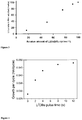
Figure 1 is a representation of the Li2CO3 deposition rate as a function of deposition temperature for an embodiment of the invention. -
Figure 2 is a representation of growth rate as a function of pulsing ratio of precursor cycles, compared to the deposition rates of binary processes according to an embodiment of the invention. There is an alternating deposition of Li and La compounds. -
Figure 3 is a representation of the compositional change of Li-La containing films as a function of pulsing ratio of each of the Li and La precursors according to an embodiment of the invention. -
Figure 4 Average growth per cycle of the LLT films as a function of the Li(t-OBu) pulse time. - The present invention will hereinafter be described with reference to the enclosed figures, tables and examples.
- The present invention discloses a method for the production of lithium-comprising thin film layers by Atomic layer deposition (hereafter ALD) wherein a substrate is to be provided by a thin preferably defect free layer of a lithium comprising compound. The method comprises pulsing of a lithium precursor into a reaction chamber wherein is arranged a substrate which is to be furnished with a lithium comprising layer. If required, an inert purge gas is pulsed through the reaction chamber after each pulse of lithium comprising precursor, or after each sequence of lithium precursor pulses, or even concurrently with the precursor. Alternatively several purge pulses may be performed between each lithium precursor pulse. In some instances purging the
chamber may be performed simply by evacuating the chamber. With each lithium precursor pulse cycle, a layer of lithium-containing material will be deposited upon the substrate such that in a layer by layer fashion the lithium-containing material will be deposited upon the substrate surface according to the ALD principle. - The main and surprising effect of the invention is that it has proven possible to deposit a lithium layer on a substrate using ALD in spite of the fact that lithium and other alkali metals are provided with a single ligand in gaseous phase for reaction. It has heretofore been thought that alkali metals would not be suitable for ALD methods as the ligand on the Li-precursor would undergo reactions with the active sites on the surface and form part of a volatile specie and not take part in a self hindering mechanism. In this way the surface would be terminated by Li-atoms who are significantly smaller than their anionic counterparts and easily be adsorbed into the film and not be able to produce a suitable terminating layer to prevent further reactions on the anionic counterparts of the film surface. This has now empirically been proven to be wrong, which is surprising and contravenes a prejudice of the art.
- Accordingly the present invention provides a new method for applying a thin film comprising an alkali metal on a surface by use of the ALD technique.
- In order for activation of the surface between each deposition cycle it may in an embodiment of the invention be necessary to include introducing an oxygen precursor in the cycle to incorporate oxygen moieties on the surface after each deposition. Any suitable oxygen precursor such as for instance water, O3 or any other oxygen comprising gaseous compound may serve the purpose as will be evident to a person skilled in the art. This oxygen containing precursor is often referred to as the oxidizer in the literature, even though there may be no clear redox reaction taking part in the main formation of the film. The oxygen precursor may be pulsed into the reaction chamber in a manner resembling that of the pulsing of the precursor material. An illustration of the rate of deposition of Li per deposition cycle according to an embodiment of the invention upon a substrate with interceding oxidisation by O3 is given in
fig. 1 . The deposition is temperature dependent, with deposition at higher temperatures being less effective than at lower temperatures. Although it is preferable to first pulse the metal phase through the reaction chamber for deposition upon the substrate, it may in some instances be preferable to pulse said oxygen comprising precursor prior to pulsing the metal comprising precursor through the chamber. The precise manner of pulsing may vary, as ALD methods, and variants thereupon, as such are known. - In one embodiment of the present invention the method and obtained thin film are characterised by comprising Li in the form of lithium oxide, as a single oxide or together with one or more other metals or metal oxides forming a metal(s)- Li- oxide thin film or together with carbon forming lithium carbonate. Where the thin film may have a layered structure.
- The deposition temperature should be adjusted such that the deposition occurs at the best possible rate, however, as is evident, the temperature must not be too high such that the substrate is damaged, or the precursor decomposes noticeable.
Fig. 1 illustrates use of Li(thd) (lithium - A separate consideration concerns the specific pulsing scheme to be used for pertaining to the duration of each pulse and to the pulse sequence. Each pulse sequence may be varied according to need, however the pulse duration of each precursor should be such that the there is sufficient time for the entire substrate surface to have reacted with the precursor. Typical precursor pulse durations may range from about 0.1 to about 20 seconds, preferably from about 0.1 to about 2 second, often about 0.8 seconds. In a similar manner, the purge pulse durations should also be tailored to ensure that the purge has been effective. Typical purge pulse durations may range from about 0.8 to about 3 seconds or longer even up to 6-12 seconds, but often the purge pulse will have a duration of 1-2 seconds. Purge pulse durations may vary significantly depending upon which precursor has been used, and whether the purging pulse occurs after a possible oxidising pulse as described above. The pulse and purge times depends mostly on the fluid dynamics of the deposition system and the chosen temperature of the precursor, i.e. its vapour pressure. A purge of the reaction chamber may be carried out in several different ways. The main importance of the purge is to avoid that there are undesirable gas phase reactions between different types of precursors. A purge may consist of an additional pulse of an inert gas capable of removing excess and unreacted precursors from the previous pulse. A purge may alternatively be carried out by evacuating the chamber by reducing the pressure and in this way remove excess and unreacted precursor from the previous pulse. Alternatively the purge may be effectuated by using the flushing effect of a carrier gas directing the precursor to the substrate and carrying away any by-products. The carrier gas may be used in a pulsevise or continuous manner. Some reactions may occur with a minimum of physisorption of excess precursor to the substrate so that a purging period may be virtually absent. The same considerations with respect to the purging pulse durations are relevant to the duration of the oxidising pulse (oxygen containing precursor), which may range from about 0.1 to about 2 seconds, preferably from about 0.5 to about 1 second, often about 1.2 seconds depending on the oxidiser. As is evident, shorter or longer pulses of each specific compound may prove necessary depending on the surface reaction kinetics as will be evident to a person skilled in the art.
- An example of a possible pulsing sequence may thus be:
- 0.8s/1.2s/1.5s/2.0s Metal-precursor/purge/oxygen-precursor/purge.
- Using these pulses in an embodiment of the invention one achieves a layer composition as described in table 1 as measured by a TOF-ERDA (time of flight elastic recoil detection analysis) method.
Table 1: Layer composition in atomic percent for an example of an embodiment of the invention Deposition temperature Li O C H Na F 185°C 33 49 17 0.22 0.33 0.25 225°C 33 48 18 0.2 0.21 0.29 - Using Li(thd) as the metal precursor and O3 as the oxidiser this results in the deposition rate as shown in
fig. 1 . The pulsing sequence is repeated as many times as is necessary in order to form the desired layer thickness. The layer thickness may be measured by any appropriate method or estimated based on empirical data. - A main purpose of the invention as such is to produce an electrolyte layer suitable for use in lithium battery applications. As such it has been considered advantageous to provide an electrolyte layer comprising further to said lithium layer a lanthanum comprising layer. Thus in an embodiment of the invention, further to the pulses of lithium comprising precursor a lanthanum comprising precursor is pulsed through the reaction chamber for reaction and subsequent deposition upon the substrate.
- Lithium as such has long been of major interest in the development of thin film batteries, in particular with respect to its use as an anode, due to its very high energy density of about 3,800 mAh/g and to its very high conductivity. However the reactive nature of Li has necessitated the use of large amounts of excess lithium due to that Li typically reacts with the electrolyte resulting in reaction losses. Previous efforts have been concentrated upon the use of LiPON (lithium phopherous oxynitride) electrolytes, however Li-La-M-O systems, where M is a metal, may present much higher lithium conductivities and would as such prove more effective than the previously studied LiPON electrolytes.
- Accordingly an object of the invention is to provide an electrolyte comprising a desired proportion of Li and La compounds using ALD methodology. This will result in a method according to the invention whereby the Li precursor and La precursor will be furnished to the reaction chamber in a predetermined sequence such that the desired composition of the layer is achieved. The specific composition may depend on which use is intended for the electrolyte as will be evident to a person skilled in the art. As for the other compounds to be deposited upon the substrate, the pulse lengths may vary and depend upon the reaction kinetics on the surface. The La precursor pulse duration may typically vary between 0.5 to about two seconds, preferably about 0.8-1.5 seconds. An example of a deposition cycle may thus be:
- 0.8-1.5s/1.2s/1.5s/2.0s Li(thd)/purge/oxygen precursor/purge
- 0.8-1.5s/1,2s/1.5s/2.0s La(thd)3/purge/oxygen precursor/purge
- Any suitable La precursor may serve as is evident to a person skilled in the art, in one embodiment of the invention the La precursor is a metal-organic La-compound. In this example use is made of a La(thd)3 precursor.
-
Figure 2 shows an illustration of the variation of the growth rate of the resulting deposited layer with respect to the percentage of Li(thd)/O3 cycles.Figure 3
correspondingly illustrates relative amount of Li deposited upon the substrate with respect to the percentage of Li(thd)/O3 cycles. - Using a TOF-ERDA measurement, it has empirically been found that the composition of the layer of each compound varies according to table 2 in this embodiment of the invention.
Table 2: Layer composition for an example of an embodiment of the invention % Li pulses La Li Li/La ratio O C H Na F 16.7 20 3 11.1 61 14 1.4 <0.1 0.4 50 15 9 36.7 58 17 1.5 0.1 0.25 75 7 22 75.9 54 16 0.6 0.8 0.4 90.9 2 30 94 50 17.5 0.3 0.5 0.33 - In one embodiment of the present invention includes further incorporating Ti into the structure thereby obtaining a Li-La-Ti-O layered compound. Ti can be included by a process similar to the La process described above but applying for instance TiCl4 as a precursor and H2O as oxygen comprising precursor. Applicable Ti precursors include for instance halogenides of Ti, Ti-Li- and Ti- organometallic or metalorganic compounds. An example of a deposition cycle may thus be:
- 8s/2s/2s/2.0s Li(t-OBu)/purge/oxygen precursor/purge
- 2s/2s/6s/3.0s La(thd)3/purge/oxygen precursor/purge
- 0.5s/1s/2s/2.0s TiCl4/purge/oxygen precursor (H2O)/purge
- This is illustrated in the following example.
- Thin films have been deposited using a F-120 Sat (ASM Mirochemistry) reactor by using La(thd)3 (thd = 2,2,6,6-tetramethyl-3,5-heptanedione, made in house according to the procedure described in [G. S. Hammond, D. C. Nonhebel, and C.-H. S. Wu, Inorg. Chem., 2 (1963) 73-76]), TiCl4 (>99.0%, Fluka), and Li(t-OBu) (t-OBu = Lithium tert-butoxide) as metal precursors and H2O (distilled) or ozone as oxygen precursors. The H2O and TiCl4 precursors were kept at room temperature in containers outside of the reactor during the depositions. The La(thd)3 and Li(t-OBu) was sublimed at 185 °C and 160 °C, respectively, and dosed into the reaction chamber using inert gas valves. All films were deposited on single crystalline substrates of Si(111) and soda lime glass substrates at a reactor temperature of 225 °C.
- Nitrogen was produced in house using a Schmidlin Nitrox 3001 generator (99.999% as to N2+Ar) and used as purging and carrier gas. The pressure of the reactor during growth was maintained at ca. 2 mbar by employing an inert gas flow of 300 cm3 min-1. Ozone was produced by feeding 99.999% O2 (AGA) into an OT-020 ozone generator from OzoneTechnology, providing an ozone concentration of 15 vol% according to specifications. An ozone flow of ca. 500 cm3min-1 was used during the ozone pulses.
- Thin films in the La-Li-Ti-O system were depositied using an intimate mixture of the cycles used for depositing the different binary oxides. These will be referred to as sub-cycles. The pulse and purge parameters for deposition of the different elements are given in the table 3 below:
Table 3: Puls and purge parameters for an example of an embodiment of the invention Element Pulse / s Purge / s H2O/O3 pulse / s Purge / s Ti 0.5 1 2 (H2O) 2 La 2 2 6 (O3) 3 Li 8 2 2 (H2O) 2 - The sub-cycles were combined in different ratios and order to control the stoichiometry of the deposit the Lithium-lanthanum-titanium-oxides (LLT).
- The pulsing order of the sub-cycles was shown to have an effect on the film growth, and a self-limiting mechanism was found when pulsing the Li-compound after the La-compound and not after the Ti-compound. ALD type of growth of lanthanum oxide and titanium oxide using La(thd)3 + ozone and TiCl4 + H2O has been described in [M. Nieminen, T. Sajavaara, E. Rauhala, M. Putkonen, and L. Niinistö, J. Mater. Chem., 11 (2001) 2340-2345.] and [J. Aarik et al., J. Cryst. Growth 148: 268 (1995), or J. Aarik, A. Aidla, V. Sammelselg, H. Siimon, T. Uustare, J. Cryst. Crowth 169 (1996) 496], respectively. The effect of Li(t-OBu) pulse time on the average growth per cycle of the films grown using a pulsing scheme of sub-cycles as: 400x(1xTi + 3xLa + 1xLi) is shown in
Figure 4. Figure 4 depictures the average growth per cycle of the LLT films as a function of the Li(t-OBu) pulse time. The growth rate stabilized at ca. 0.048 nm/cycle for films deposited using at least 8 s pulse of Li(t-OBu). - The composition of the films was analyzed by TOF-ERDA (Time-of-Flight Energy Recoil Detection Analysis) and stabilized at ca. Li0.34La0.30TiO2.9 for films deposited with more than 8 s of Li(t-OBu) pulse. In addition to these elements the films contained some chlorine (3.0-3.7 at.%) carbon (1.9-3.0 at.%) and hydrogen (0.7-2.5 at.%) as impurities. Analysis performed by Leila Costelle, Department of Physics, University of Helsinki, Finland.
- Equivalent to this process other metal organic, organo metallic, or halogenides may be included in the Li comprising film.
- It is thus to a large degree possible to design the electrolyte according to the needs of the task. Amongst possible uses for this electrolyte are as a thin-film barrier between Li layers in a thin-film battery, and it is one of the objects of the present invention to provide such an electrolyte. Although battery technology is one of the possible uses of the present method, it should be clear that other possible uses of the ALD method for depositing Li-layers on a substrate are foreseen. Although exemplified above for use in a battery this will not be the only application for the present invention.
- The present invention has thus proposed a method for the formation of thin Li- comprising layers on a substrate using an ALD-method.
Claims (11)
- A method for formation of a Li-comprising layer on a substrate by atomic layer deposition comprising the following steps:a) providing a substrate in a reaction chamber wherein said reaction chamber is arranged for gas-to-surface reactions,b) pulsing a lithium precursor through said reaction chamber,c) reacting said lithium precursor with at least one surface of said substrate,d) purging of said reaction chamberd1) by sending a purge gas through said reaction chamber for the purging of the reaction chamber ord2) by evacuating said chamber, ande) repeating steps b) to d) a desired number of times in order for the formation of a thin film layer of a lithium comprising material upon said at least one surface of said substrate,wherein the lithium precursor is selected from among lithium 2,2,6,6-tetramethylheptane-3,5-dionate, lithium alkoxides, lithium alkyls, cyclic lithium compounds, lithium dicyclohexamide, and bimetallic or multimetallic compounds.
- A method according to claim 1 wherein steps b) through d) are repeated with independently chosen lithium precursors in step b).
- A method according to claim 1, wherein an oxidising gas is pulsed through said reaction chamber such that the resulting deposition sequence comprisesa) providing a substrate in a reaction chamber wherein said reaction chamber is arranged for gas-to-surface reactions,b) pulsing a lithium precursor through said reaction chamber,c) reacting said lithium precursor with at least one surface of the substrate,d) purging of said reaction chamber,e) pulsing an oxygen precursor through said reaction chamber,f) reacting said oxygen precursor with said at least one surface of said substrate,g) purging of said reaction chamber,h) repeating steps b) to g) a desired number of times in order for the formation of a thin film layer of a lithium comprising material upon said at least one surface of said substrate,where the purging of said chamber may be performed by sending a purge gas through said reaction chamber for the purging of the reaction chamber or by evacuating said chamber.
- A method according to claim 3 wherein further to the described steps, a lanthanum comprising precursor is pulsed through the reaction chamber such that the reaction resulting sequence comprises:a) providing a substrate in a reaction chamber wherein said reaction chamber is arranged for gas-to-surface reactions,b) pulsing a lanthanum precursor through said reaction chamber,c) reacting said lanthanum precursor with said at least one surface of said substrate,d) purging of said reaction chamber,e) pulsing an oxygen precursor through said reaction chamber,f) reacting said oxygen precursor with said at least one surface of said substrate,g) purging of said reaction chamber,h) pulsing a lithium precursor through said reaction chamber,i) reacting said lithium precursor with a surface layer of the substrate,j) purging of said reaction chamber,k) pulsing an oxygen precursor through said reaction chamber,l) reacting said oxygen precursor with said at least one surface of said substrate,m) purging of said reaction chamber,n) repeating steps b) to m) a desired number of times in order for the formation of a thin film layer of a lithium and lanthanum comprising material upon said at least one surface of said substrate,where the purging of said chamber may be performed by sending a purge gas through said reaction chamber for the purging of the reaction chamber or by evacuating said chamber.
- A method according to claim 4 wherein further to the described steps, a titanium comprising precursor is pulsed through the reaction chamber such that the reaction resulting sequence comprises:a) providing a substrate in a reaction chamber wherein said reaction chamber is arranged for gas-to-surface reactions,b) pulsing a lanthanum precursor through said reaction chamber,c) reacting said lanthanum precursor with said at least one surface of said substrate,d) purging of said reaction chamber,e) pulsing an oxygen precursor through said reaction chamber,f) reacting said oxygen precursor with said at least one surface of said substrate,g) purging of said reaction chamber,h) pulsing a lithium precursor through said reaction chamber,i) reacting said lithium precursor with a surface layer of the substrate,j) purging of said reaction chamber,k) pulsing an oxygen precursor through said reaction chamber,l) reacting said oxygen precursor with said at least one surface of said substrate,m) purging of said reaction chamber,n) pulsing a titanium precursor through said reaction chamber,o) reacting said titanium precursor with said at least one surface of said substrate,p) purging of said reaction chamber,q) pulsing an oxygen precursor through said reaction chamber,r) reacting said oxygen precursor with said at least one surface of said substrate,s) purging of said reaction chamber,t) repeating steps b) to s) a desired number of times in order for the formation of a thin film layer of a lithium, lanthanum and titanium comprising material upon said at least one surface of said substrate,where the purging of said chamber may be performed by sending a purge gas through said reaction chamber for the purging of the reaction chamber or by evacuating said chamber.
- A method according to any one of the previous claims, wherein each step of the process is independently repeated a desired number of times.
- A method according to claim 6, where the groups of steps b)-g), f)-m) and n)-s) respectively are independently repeated one or more times before continuing the sequence.
- A method according to any one of the preceding claims, where the thin film layer is an oxide or a carbonate layer or a mixture thereof.
- A method according to claim 5, 6, 7 or 8 for the production of a La-Li-Ti-O layered thin film.
- A method according to any of the above claims for the production of a lithium-comprising thin film battery.
- A method according to any of the above claims for the production of a lithium-comprising electrolyte thin film for use in a battery.
Priority Applications (1)
| Application Number | Priority Date | Filing Date | Title |
|---|---|---|---|
| PL08866667T PL2225407T3 (en) | 2007-12-28 | 2008-12-23 | Formation of a lithium comprising structure on a substrate by ald |
Applications Claiming Priority (2)
| Application Number | Priority Date | Filing Date | Title |
|---|---|---|---|
| NO20076696 | 2007-12-28 | ||
| PCT/NO2008/000468 WO2009084966A1 (en) | 2007-12-28 | 2008-12-23 | Formation of a lithium comprising structure on a substrate by ald |
Publications (3)
| Publication Number | Publication Date |
|---|---|
| EP2225407A1 EP2225407A1 (en) | 2010-09-08 |
| EP2225407A4 EP2225407A4 (en) | 2012-11-21 |
| EP2225407B1 true EP2225407B1 (en) | 2017-05-31 |
Family
ID=40824531
Family Applications (1)
| Application Number | Title | Priority Date | Filing Date |
|---|---|---|---|
| EP08866667.2A Active EP2225407B1 (en) | 2007-12-28 | 2008-12-23 | Formation of a lithium comprising structure on a substrate by ald |
Country Status (7)
| Country | Link |
|---|---|
| US (4) | US8894723B2 (en) |
| EP (1) | EP2225407B1 (en) |
| JP (1) | JP5442635B2 (en) |
| DK (1) | DK2225407T3 (en) |
| ES (1) | ES2638614T3 (en) |
| PL (1) | PL2225407T3 (en) |
| WO (1) | WO2009084966A1 (en) |
Families Citing this family (34)
| Publication number | Priority date | Publication date | Assignee | Title |
|---|---|---|---|---|
| US8894723B2 (en) * | 2007-12-28 | 2014-11-25 | Universitetet I Oslo | Formation of a lithium comprising structure on a substrate by ALD |
| WO2011002920A2 (en) * | 2009-07-01 | 2011-01-06 | L'air Liquide, Societe Anonyme Pour L'etude Et L'exploitation Des Procedes Georges Claude | LITHIUM PRECURSORS FOR LixMyOz MATERIALS FOR BATTERIES |
| WO2011158948A1 (en) * | 2010-06-18 | 2011-12-22 | Semiconductor Energy Laboratory Co., Ltd. | Method of manufacturing power storage device |
| JP5963456B2 (en) * | 2011-02-18 | 2016-08-03 | 株式会社日立国際電気 | Semiconductor device manufacturing method, substrate processing apparatus, and substrate processing method |
| US9315894B2 (en) | 2011-03-30 | 2016-04-19 | Asm Ip Holding B.V. | Atomic layer deposition of metal phosphates and lithium silicates |
| WO2013011297A1 (en) | 2011-07-15 | 2013-01-24 | Universitetet I Oslo | Method |
| US9382615B2 (en) | 2012-10-12 | 2016-07-05 | Asm Ip Holding B.V. | Vapor deposition of LiF thin films |
| US9755235B2 (en) | 2014-07-17 | 2017-09-05 | Ada Technologies, Inc. | Extreme long life, high energy density batteries and method of making and using the same |
| WO2016209460A2 (en) | 2015-05-21 | 2016-12-29 | Ada Technologies, Inc. | High energy density hybrid pseudocapacitors and method of making and using the same |
| US11996564B2 (en) | 2015-06-01 | 2024-05-28 | Forge Nano Inc. | Nano-engineered coatings for anode active materials, cathode active materials, and solid-state electrolytes and methods of making batteries containing nano-engineered coatings |
| US12027661B2 (en) | 2015-06-01 | 2024-07-02 | Forge Nano Inc. | Nano-engineered coatings for anode active materials, cathode active materials, and solid-state electrolytes and methods of making batteries containing nano-engineered coatings |
| US12401042B2 (en) | 2015-06-01 | 2025-08-26 | Forge Nano Inc. | Nano-engineered coatings for anode active materials, cathode active materials, and solid-state electrolytes and methods of making batteries containing nano-engineered coatings |
| US9809490B2 (en) | 2015-07-02 | 2017-11-07 | Panasonic Intellectual Property Management Co., Ltd. | Method for producing oxynitride film by atomic layer deposition process |
| US10692659B2 (en) | 2015-07-31 | 2020-06-23 | Ada Technologies, Inc. | High energy and power electrochemical device and method of making and using same |
| JP6540569B2 (en) | 2016-03-23 | 2019-07-10 | トヨタ自動車株式会社 | Lithium ion battery and method of manufacturing the same |
| JP6782461B2 (en) * | 2016-03-31 | 2020-11-11 | パナソニックIpマネジメント株式会社 | Negative electrode active material for non-aqueous electrolyte secondary batteries |
| CN107579275B (en) | 2016-07-04 | 2022-02-11 | 松下知识产权经营株式会社 | Solid electrolyte containing oxynitride and secondary battery using the same |
| CN109565032B (en) | 2016-09-23 | 2022-01-11 | 松下知识产权经营株式会社 | Negative electrode for nonaqueous electrolyte secondary battery, and method for producing negative electrode for nonaqueous electrolyte secondary battery |
| WO2018163519A1 (en) | 2017-03-06 | 2018-09-13 | パナソニックIpマネジメント株式会社 | Positive electrode active material and battery |
| US11024846B2 (en) | 2017-03-23 | 2021-06-01 | Ada Technologies, Inc. | High energy/power density, long cycle life, safe lithium-ion battery capable of long-term deep discharge/storage near zero volt and method of making and using the same |
| US20180301743A1 (en) * | 2017-04-18 | 2018-10-18 | Tubz, Llc | Method and apparatus for manufacturing energy storage devices |
| CN110199418B (en) | 2017-04-24 | 2024-03-08 | 松下知识产权经营株式会社 | Cathode active material and battery |
| CN110214389B (en) | 2017-05-29 | 2023-06-20 | 松下知识产权经营株式会社 | Positive electrode active material and battery |
| US11894546B2 (en) | 2017-05-31 | 2024-02-06 | The Board Of Trustees Of The Leland Stanford Junior University | Atomic layer deposition of stable lithium ion conductive interfacial layer for stable cathode cycling |
| JP7228771B2 (en) | 2017-07-27 | 2023-02-27 | パナソニックIpマネジメント株式会社 | Positive electrode active material and battery |
| JP7241287B2 (en) | 2017-07-27 | 2023-03-17 | パナソニックIpマネジメント株式会社 | Positive electrode active material and battery |
| KR101989858B1 (en) * | 2017-12-07 | 2019-06-17 | 한국해양대학교 산학협력단 | Lithium-carbon composite having cavities formed therein and method for manufacturing the same |
| JP7228773B2 (en) | 2018-01-17 | 2023-02-27 | パナソニックIpマネジメント株式会社 | Positive electrode active material and battery |
| GB201910404D0 (en) * | 2019-07-19 | 2019-09-04 | Univ Oslo | Method |
| TWI862702B (en) * | 2019-10-08 | 2024-11-21 | 法商液態空氣喬治斯克勞帝方法研究開發股份有限公司 | Lithium precursors for deposition of lithium-containing layers, islets or clusters and methods of using the same |
| EP4101017A4 (en) * | 2020-02-06 | 2023-08-02 | Bar Ilan University | <sup2/>? <sub2/>?x?method for production of lisi <ns1:sub>y</ns1:sub>?o <ns2:sub>z</ns2:sub>?coatings using a single source for li and si and resultant coated products |
| FR3114915B1 (en) * | 2020-10-01 | 2022-10-21 | Univ Lille | Process for manufacturing a lithiated material in thin layers |
| US12374678B2 (en) * | 2020-12-03 | 2025-07-29 | Elevated Materials Us Llc | Lithium metal surface modification using carbonate passivation |
| EP4040523B1 (en) * | 2021-02-03 | 2025-03-26 | Imec VZW | Coated cathode |
Family Cites Families (17)
| Publication number | Priority date | Publication date | Assignee | Title |
|---|---|---|---|---|
| US6197450B1 (en) | 1998-10-22 | 2001-03-06 | Ramot University Authority For Applied Research & Industrial Development Ltd. | Micro electrochemical energy storage cells |
| WO2002027063A2 (en) * | 2000-09-28 | 2002-04-04 | President And Fellows Of Harward College | Vapor deposition of oxides, silicates and phosphates |
| JP2002289353A (en) * | 2001-03-26 | 2002-10-04 | Pioneer Electronic Corp | Organic semiconductor diode |
| KR100431740B1 (en) * | 2001-09-14 | 2004-05-17 | 주식회사 하이닉스반도체 | Semiconductor with High-k dielectric layer and Method for fabricating the same |
| EP2182088B1 (en) * | 2002-11-15 | 2013-07-17 | President and Fellows of Harvard College | Atomic layer deposition using metal amidinates |
| US6818517B1 (en) * | 2003-08-29 | 2004-11-16 | Asm International N.V. | Methods of depositing two or more layers on a substrate in situ |
| EP1665425B1 (en) * | 2003-09-15 | 2007-06-06 | Koninklijke Philips Electronics N.V. | Electrochemical energy source, electronic device and method of manufacturing said energy source |
| WO2005061410A1 (en) * | 2003-12-23 | 2005-07-07 | Aalborg Universitet | Method and apparatus for production of a compound having submicron particle size and a compound produced by the method |
| KR20040037053A (en) * | 2004-04-16 | 2004-05-04 | 주식회사 이스퀘어텍 | Electrolyte for Lithium Rechargeable Battery to Control Swelling |
| WO2006056963A2 (en) | 2004-11-26 | 2006-06-01 | Koninklijke Philips Electronics N.V. | Energy system, electronic module, electronic device, and method for manufacturing of said energy system |
| CN101065830A (en) * | 2004-11-26 | 2007-10-31 | 皇家飞利浦电子股份有限公司 | Method and electronic device for surface area modification |
| NO20045674D0 (en) * | 2004-12-28 | 2004-12-28 | Uni I Oslo | Thin films prepared with gas phase deposition technique |
| EP1859503A1 (en) * | 2005-03-03 | 2007-11-28 | Koninklijke Philips Electronics N.V. | Method of manufacturing an electrochemical energy source, electrochemical energy source thus obtained and electronic device |
| US20090286674A1 (en) | 2006-06-19 | 2009-11-19 | Universitetet I Oslo | Activation of surfaces through gas phase reactions |
| KR20090125256A (en) * | 2007-03-26 | 2009-12-04 | 사임베트 코퍼레이션 | Substrate for lithium thin film battery |
| US8894723B2 (en) * | 2007-12-28 | 2014-11-25 | Universitetet I Oslo | Formation of a lithium comprising structure on a substrate by ALD |
| TWI365562B (en) * | 2008-10-03 | 2012-06-01 | Ind Tech Res Inst | Positive electrode and method for manufacturing the same and lithium battery utilizing the same |
-
2008
- 2008-12-23 US US12/810,897 patent/US8894723B2/en not_active Ceased
- 2008-12-23 DK DK08866667.2T patent/DK2225407T3/en active
- 2008-12-23 EP EP08866667.2A patent/EP2225407B1/en active Active
- 2008-12-23 US US16/258,197 patent/USRE48853E1/en active Active
- 2008-12-23 US US15/806,846 patent/USRE47325E1/en active Active
- 2008-12-23 US US15/360,153 patent/USRE46610E1/en active Active
- 2008-12-23 WO PCT/NO2008/000468 patent/WO2009084966A1/en not_active Ceased
- 2008-12-23 PL PL08866667T patent/PL2225407T3/en unknown
- 2008-12-23 JP JP2010540607A patent/JP5442635B2/en active Active
- 2008-12-23 ES ES08866667.2T patent/ES2638614T3/en active Active
Also Published As
| Publication number | Publication date |
|---|---|
| USRE46610E1 (en) | 2017-11-14 |
| DK2225407T3 (en) | 2017-09-18 |
| EP2225407A4 (en) | 2012-11-21 |
| USRE48853E1 (en) | 2021-12-14 |
| US8894723B2 (en) | 2014-11-25 |
| EP2225407A1 (en) | 2010-09-08 |
| WO2009084966A1 (en) | 2009-07-09 |
| US20110099798A1 (en) | 2011-05-05 |
| USRE47325E1 (en) | 2019-03-26 |
| JP5442635B2 (en) | 2014-03-12 |
| ES2638614T3 (en) | 2017-10-23 |
| PL2225407T3 (en) | 2017-12-29 |
| JP2011508826A (en) | 2011-03-17 |
Similar Documents
| Publication | Publication Date | Title |
|---|---|---|
| US8894723B2 (en) | Formation of a lithium comprising structure on a substrate by ALD | |
| US9765431B2 (en) | Atomic layer deposition of metal phosphates and lithium silicates | |
| Elam et al. | Growth of ZnO/Al2O3 alloy films using atomic layer deposition techniques | |
| Hämäläinen et al. | Lithium phosphate thin films grown by atomic layer deposition | |
| Putkonen et al. | Surface-controlled deposition of Sc2O3 thin films by atomic layer epitaxy using β-diketonate and organometallic precursors | |
| Pilvi et al. | Novel ALD process for depositing CaF2 thin films | |
| US10311992B2 (en) | Transparent conducting films including complex oxides | |
| Miikkulainen et al. | Atomic layer deposition of Li x Ti y O z thin films | |
| US9909211B2 (en) | Vapor deposition of LiF thin films | |
| Seppälä et al. | Heteroleptic cyclopentadienyl-amidinate precursors for atomic layer deposition (ALD) of Y, Pr, Gd, and Dy oxide thin films | |
| Hämäläinen et al. | Atomic layer deposition of iridium oxide thin films from Ir (acac) 3 and ozone | |
| EP1433874A2 (en) | Method for metal oxide thin film deposition via MOCVD | |
| Madadi et al. | Atomic and molecular layer deposition of alkaLi metal based thin films | |
| Mäntymäki et al. | Metal fluorides as lithium-ion battery materials: an atomic layer deposition perspective | |
| Zhao et al. | Thermal and plasma-enhanced atomic layer deposition of yttrium oxide films and the properties of water wettability | |
| Kukli et al. | Atomic layer deposition of tantalum oxide thin films from iodide precursor | |
| WO2013011297A1 (en) | Method | |
| US20060088660A1 (en) | Methods of depositing lead containing oxides films | |
| Knapas et al. | Etching of Nb2O5 thin films by NbCl5 | |
| Park et al. | Study of a vanadium precursor for VO2 thin-film growth in the atomic layer deposition process by multiscale simulations | |
| US20220259730A1 (en) | Method | |
| EP1607498B1 (en) | Method for forming oxide coating film, oxide coating film and coating film structure | |
| JP3104613B2 (en) | Method for producing bismuth layered compound | |
| KR20070072927A (en) | How to deposit lead-containing oxide thin film | |
| Aarik | Atomic layer deposition of titanium, zirconium and hafnium dioxides: growth mechanisms and properties of thin films |
Legal Events
| Date | Code | Title | Description |
|---|---|---|---|
| PUAI | Public reference made under article 153(3) epc to a published international application that has entered the european phase |
Free format text: ORIGINAL CODE: 0009012 |
|
| 17P | Request for examination filed |
Effective date: 20100625 |
|
| AK | Designated contracting states |
Kind code of ref document: A1 Designated state(s): AT BE BG CH CY CZ DE DK EE ES FI FR GB GR HR HU IE IS IT LI LT LU LV MC MT NL NO PL PT RO SE SI SK TR |
|
| AX | Request for extension of the european patent |
Extension state: AL BA MK RS |
|
| RIN1 | Information on inventor provided before grant (corrected) |
Inventor name: PUTKONEN ,MALTI Inventor name: NILSEN, OLA Inventor name: FJELLVAG, HELMER Inventor name: AALTONEN, TITTA Inventor name: ALNES, MARI, ENDRESEN |
|
| RIN1 | Information on inventor provided before grant (corrected) |
Inventor name: PUTKONEN ,MALTI Inventor name: AALTONEN, TITTA Inventor name: NILSEN, OLA Inventor name: ALNES, MARI, ENDRESEN Inventor name: FJELLVAG, HELMER |
|
| DAX | Request for extension of the european patent (deleted) | ||
| A4 | Supplementary search report drawn up and despatched |
Effective date: 20121022 |
|
| RIC1 | Information provided on ipc code assigned before grant |
Ipc: H01M 10/04 20060101ALI20121016BHEP Ipc: C23C 16/40 20060101AFI20121016BHEP Ipc: H01M 4/04 20060101ALI20121016BHEP Ipc: C23C 16/455 20060101ALI20121016BHEP |
|
| 17Q | First examination report despatched |
Effective date: 20121217 |
|
| REG | Reference to a national code |
Ref country code: DE Ref legal event code: R079 Ref document number: 602008050525 Country of ref document: DE Free format text: PREVIOUS MAIN CLASS: C23C0016400000 Ipc: H01M0010056200 |
|
| GRAP | Despatch of communication of intention to grant a patent |
Free format text: ORIGINAL CODE: EPIDOSNIGR1 |
|
| RIC1 | Information provided on ipc code assigned before grant |
Ipc: H01M 6/40 20060101ALI20160530BHEP Ipc: H01M 10/04 20060101ALI20160530BHEP Ipc: C23C 16/40 20060101ALI20160530BHEP Ipc: H01M 6/18 20060101ALI20160530BHEP Ipc: H01M 10/0562 20100101AFI20160530BHEP Ipc: C23C 16/455 20060101ALI20160530BHEP Ipc: H01M 4/04 20060101ALI20160530BHEP |
|
| INTG | Intention to grant announced |
Effective date: 20160707 |
|
| GRAJ | Information related to disapproval of communication of intention to grant by the applicant or resumption of examination proceedings by the epo deleted |
Free format text: ORIGINAL CODE: EPIDOSDIGR1 |
|
| GRAP | Despatch of communication of intention to grant a patent |
Free format text: ORIGINAL CODE: EPIDOSNIGR1 |
|
| INTC | Intention to grant announced (deleted) | ||
| RIN1 | Information on inventor provided before grant (corrected) |
Inventor name: FJELLVAG, HELMER Inventor name: PUTKONEN, MATTI Inventor name: ALNES, MARI ENDRESEN Inventor name: AALTONEN, TITTA Inventor name: NILSEN, OLA |
|
| INTG | Intention to grant announced |
Effective date: 20161212 |
|
| GRAS | Grant fee paid |
Free format text: ORIGINAL CODE: EPIDOSNIGR3 |
|
| GRAA | (expected) grant |
Free format text: ORIGINAL CODE: 0009210 |
|
| AK | Designated contracting states |
Kind code of ref document: B1 Designated state(s): AT BE BG CH CY CZ DE DK EE ES FI FR GB GR HR HU IE IS IT LI LT LU LV MC MT NL NO PL PT RO SE SI SK TR |
|
| REG | Reference to a national code |
Ref country code: CH Ref legal event code: EP Ref country code: GB Ref legal event code: FG4D |
|
| REG | Reference to a national code |
Ref country code: AT Ref legal event code: REF Ref document number: 898198 Country of ref document: AT Kind code of ref document: T Effective date: 20170615 |
|
| REG | Reference to a national code |
Ref country code: IE Ref legal event code: FG4D |
|
| REG | Reference to a national code |
Ref country code: DE Ref legal event code: R096 Ref document number: 602008050525 Country of ref document: DE |
|
| REG | Reference to a national code |
Ref country code: SE Ref legal event code: TRGR |
|
| REG | Reference to a national code |
Ref country code: NL Ref legal event code: FP |
|
| REG | Reference to a national code |
Ref country code: DK Ref legal event code: T3 Effective date: 20170912 |
|
| REG | Reference to a national code |
Ref country code: LT Ref legal event code: MG4D |
|
| REG | Reference to a national code |
Ref country code: AT Ref legal event code: MK05 Ref document number: 898198 Country of ref document: AT Kind code of ref document: T Effective date: 20170531 |
|
| REG | Reference to a national code |
Ref country code: ES Ref legal event code: FG2A Ref document number: 2638614 Country of ref document: ES Kind code of ref document: T3 Effective date: 20171023 |
|
| REG | Reference to a national code |
Ref country code: NO Ref legal event code: T2 Effective date: 20170531 |
|
| PG25 | Lapsed in a contracting state [announced via postgrant information from national office to epo] |
Ref country code: HR Free format text: LAPSE BECAUSE OF FAILURE TO SUBMIT A TRANSLATION OF THE DESCRIPTION OR TO PAY THE FEE WITHIN THE PRESCRIBED TIME-LIMIT Effective date: 20170531 Ref country code: AT Free format text: LAPSE BECAUSE OF FAILURE TO SUBMIT A TRANSLATION OF THE DESCRIPTION OR TO PAY THE FEE WITHIN THE PRESCRIBED TIME-LIMIT Effective date: 20170531 Ref country code: GR Free format text: LAPSE BECAUSE OF FAILURE TO SUBMIT A TRANSLATION OF THE DESCRIPTION OR TO PAY THE FEE WITHIN THE PRESCRIBED TIME-LIMIT Effective date: 20170901 Ref country code: LT Free format text: LAPSE BECAUSE OF FAILURE TO SUBMIT A TRANSLATION OF THE DESCRIPTION OR TO PAY THE FEE WITHIN THE PRESCRIBED TIME-LIMIT Effective date: 20170531 |
|
| PG25 | Lapsed in a contracting state [announced via postgrant information from national office to epo] |
Ref country code: IS Free format text: LAPSE BECAUSE OF FAILURE TO SUBMIT A TRANSLATION OF THE DESCRIPTION OR TO PAY THE FEE WITHIN THE PRESCRIBED TIME-LIMIT Effective date: 20170930 Ref country code: LV Free format text: LAPSE BECAUSE OF FAILURE TO SUBMIT A TRANSLATION OF THE DESCRIPTION OR TO PAY THE FEE WITHIN THE PRESCRIBED TIME-LIMIT Effective date: 20170531 Ref country code: BG Free format text: LAPSE BECAUSE OF FAILURE TO SUBMIT A TRANSLATION OF THE DESCRIPTION OR TO PAY THE FEE WITHIN THE PRESCRIBED TIME-LIMIT Effective date: 20170831 |
|
| REG | Reference to a national code |
Ref country code: FR Ref legal event code: PLFP Year of fee payment: 10 |
|
| PG25 | Lapsed in a contracting state [announced via postgrant information from national office to epo] |
Ref country code: CZ Free format text: LAPSE BECAUSE OF FAILURE TO SUBMIT A TRANSLATION OF THE DESCRIPTION OR TO PAY THE FEE WITHIN THE PRESCRIBED TIME-LIMIT Effective date: 20170531 Ref country code: RO Free format text: LAPSE BECAUSE OF FAILURE TO SUBMIT A TRANSLATION OF THE DESCRIPTION OR TO PAY THE FEE WITHIN THE PRESCRIBED TIME-LIMIT Effective date: 20170531 Ref country code: EE Free format text: LAPSE BECAUSE OF FAILURE TO SUBMIT A TRANSLATION OF THE DESCRIPTION OR TO PAY THE FEE WITHIN THE PRESCRIBED TIME-LIMIT Effective date: 20170531 Ref country code: SK Free format text: LAPSE BECAUSE OF FAILURE TO SUBMIT A TRANSLATION OF THE DESCRIPTION OR TO PAY THE FEE WITHIN THE PRESCRIBED TIME-LIMIT Effective date: 20170531 |
|
| REG | Reference to a national code |
Ref country code: DE Ref legal event code: R097 Ref document number: 602008050525 Country of ref document: DE |
|
| PLBE | No opposition filed within time limit |
Free format text: ORIGINAL CODE: 0009261 |
|
| STAA | Information on the status of an ep patent application or granted ep patent |
Free format text: STATUS: NO OPPOSITION FILED WITHIN TIME LIMIT |
|
| 26N | No opposition filed |
Effective date: 20180301 |
|
| PG25 | Lapsed in a contracting state [announced via postgrant information from national office to epo] |
Ref country code: SI Free format text: LAPSE BECAUSE OF FAILURE TO SUBMIT A TRANSLATION OF THE DESCRIPTION OR TO PAY THE FEE WITHIN THE PRESCRIBED TIME-LIMIT Effective date: 20170531 |
|
| REG | Reference to a national code |
Ref country code: IE Ref legal event code: MM4A |
|
| PG25 | Lapsed in a contracting state [announced via postgrant information from national office to epo] |
Ref country code: LU Free format text: LAPSE BECAUSE OF NON-PAYMENT OF DUE FEES Effective date: 20171223 Ref country code: MT Free format text: LAPSE BECAUSE OF NON-PAYMENT OF DUE FEES Effective date: 20171223 |
|
| REG | Reference to a national code |
Ref country code: BE Ref legal event code: MM Effective date: 20171231 |
|
| PG25 | Lapsed in a contracting state [announced via postgrant information from national office to epo] |
Ref country code: IE Free format text: LAPSE BECAUSE OF NON-PAYMENT OF DUE FEES Effective date: 20171223 |
|
| PG25 | Lapsed in a contracting state [announced via postgrant information from national office to epo] |
Ref country code: BE Free format text: LAPSE BECAUSE OF NON-PAYMENT OF DUE FEES Effective date: 20171231 |
|
| PG25 | Lapsed in a contracting state [announced via postgrant information from national office to epo] |
Ref country code: HU Free format text: LAPSE BECAUSE OF FAILURE TO SUBMIT A TRANSLATION OF THE DESCRIPTION OR TO PAY THE FEE WITHIN THE PRESCRIBED TIME-LIMIT; INVALID AB INITIO Effective date: 20081223 Ref country code: MC Free format text: LAPSE BECAUSE OF FAILURE TO SUBMIT A TRANSLATION OF THE DESCRIPTION OR TO PAY THE FEE WITHIN THE PRESCRIBED TIME-LIMIT Effective date: 20170531 |
|
| PG25 | Lapsed in a contracting state [announced via postgrant information from national office to epo] |
Ref country code: CY Free format text: LAPSE BECAUSE OF NON-PAYMENT OF DUE FEES Effective date: 20170531 |
|
| PG25 | Lapsed in a contracting state [announced via postgrant information from national office to epo] |
Ref country code: TR Free format text: LAPSE BECAUSE OF FAILURE TO SUBMIT A TRANSLATION OF THE DESCRIPTION OR TO PAY THE FEE WITHIN THE PRESCRIBED TIME-LIMIT Effective date: 20170531 |
|
| PG25 | Lapsed in a contracting state [announced via postgrant information from national office to epo] |
Ref country code: PT Free format text: LAPSE BECAUSE OF FAILURE TO SUBMIT A TRANSLATION OF THE DESCRIPTION OR TO PAY THE FEE WITHIN THE PRESCRIBED TIME-LIMIT Effective date: 20170531 |
|
| P01 | Opt-out of the competence of the unified patent court (upc) registered |
Effective date: 20230428 |
|
| PGFP | Annual fee paid to national office [announced via postgrant information from national office to epo] |
Ref country code: SE Payment date: 20231221 Year of fee payment: 16 Ref country code: NO Payment date: 20231220 Year of fee payment: 16 Ref country code: IT Payment date: 20231228 Year of fee payment: 16 Ref country code: DK Payment date: 20231219 Year of fee payment: 16 |
|
| PGFP | Annual fee paid to national office [announced via postgrant information from national office to epo] |
Ref country code: ES Payment date: 20240118 Year of fee payment: 16 |
|
| PGFP | Annual fee paid to national office [announced via postgrant information from national office to epo] |
Ref country code: CH Payment date: 20240101 Year of fee payment: 16 |
|
| REG | Reference to a national code |
Ref country code: DK Ref legal event code: EBP Effective date: 20241231 |
|
| REG | Reference to a national code |
Ref country code: SE Ref legal event code: EUG |
|
| REG | Reference to a national code |
Ref country code: CH Ref legal event code: PL |
|
| PG25 | Lapsed in a contracting state [announced via postgrant information from national office to epo] |
Ref country code: NO Free format text: LAPSE BECAUSE OF NON-PAYMENT OF DUE FEES Effective date: 20241231 Ref country code: IT Free format text: LAPSE BECAUSE OF NON-PAYMENT OF DUE FEES Effective date: 20241223 |
|
| PG25 | Lapsed in a contracting state [announced via postgrant information from national office to epo] |
Ref country code: CH Free format text: LAPSE BECAUSE OF NON-PAYMENT OF DUE FEES Effective date: 20241231 |
|
| PGFP | Annual fee paid to national office [announced via postgrant information from national office to epo] |
Ref country code: GB Payment date: 20251218 Year of fee payment: 18 |
|
| PG25 | Lapsed in a contracting state [announced via postgrant information from national office to epo] |
Ref country code: DK Free format text: LAPSE BECAUSE OF NON-PAYMENT OF DUE FEES Effective date: 20241231 |
|
| PGFP | Annual fee paid to national office [announced via postgrant information from national office to epo] |
Ref country code: FI Payment date: 20251218 Year of fee payment: 18 |
|
| PGFP | Annual fee paid to national office [announced via postgrant information from national office to epo] |
Ref country code: NL Payment date: 20251223 Year of fee payment: 18 Ref country code: FR Payment date: 20251217 Year of fee payment: 18 |
|
| PGFP | Annual fee paid to national office [announced via postgrant information from national office to epo] |
Ref country code: PL Payment date: 20251215 Year of fee payment: 18 |
|
| REG | Reference to a national code |
Ref country code: ES Ref legal event code: FD2A Effective date: 20260204 |
|
| PG25 | Lapsed in a contracting state [announced via postgrant information from national office to epo] |
Ref country code: ES Free format text: LAPSE BECAUSE OF NON-PAYMENT OF DUE FEES Effective date: 20241224 |
|
| PGFP | Annual fee paid to national office [announced via postgrant information from national office to epo] |
Ref country code: DE Payment date: 20251222 Year of fee payment: 18 |