EP2223789A2 - In-mold type RF antenna, device including the same, and associated methods - Google Patents
In-mold type RF antenna, device including the same, and associated methods Download PDFInfo
- Publication number
- EP2223789A2 EP2223789A2 EP10153183A EP10153183A EP2223789A2 EP 2223789 A2 EP2223789 A2 EP 2223789A2 EP 10153183 A EP10153183 A EP 10153183A EP 10153183 A EP10153183 A EP 10153183A EP 2223789 A2 EP2223789 A2 EP 2223789A2
- Authority
- EP
- European Patent Office
- Prior art keywords
- antenna
- film
- mold
- disposing
- case
- Prior art date
- Legal status (The legal status is an assumption and is not a legal conclusion. Google has not performed a legal analysis and makes no representation as to the accuracy of the status listed.)
- Granted
Links
- 238000000034 method Methods 0.000 title claims abstract description 27
- RYGMFSIKBFXOCR-UHFFFAOYSA-N Copper Chemical compound [Cu] RYGMFSIKBFXOCR-UHFFFAOYSA-N 0.000 claims abstract description 22
- 239000011889 copper foil Substances 0.000 claims abstract description 22
- 229920005989 resin Polymers 0.000 claims abstract description 20
- 239000011347 resin Substances 0.000 claims abstract description 20
- 239000000853 adhesive Substances 0.000 claims description 16
- 230000001070 adhesive effect Effects 0.000 claims description 16
- 239000012790 adhesive layer Substances 0.000 claims description 10
- 238000004519 manufacturing process Methods 0.000 claims description 10
- -1 polyethylene terephthalate Polymers 0.000 claims description 10
- 239000011248 coating agent Substances 0.000 claims description 6
- 238000000576 coating method Methods 0.000 claims description 6
- 238000005530 etching Methods 0.000 claims description 5
- 229920000139 polyethylene terephthalate Polymers 0.000 claims description 4
- 239000005020 polyethylene terephthalate Substances 0.000 claims description 4
- 229920001721 polyimide Polymers 0.000 claims description 4
- 239000004593 Epoxy Substances 0.000 claims description 3
- 239000004952 Polyamide Substances 0.000 claims description 3
- 239000004734 Polyphenylene sulfide Substances 0.000 claims description 3
- 125000000951 phenoxy group Chemical group [H]C1=C([H])C([H])=C(O*)C([H])=C1[H] 0.000 claims description 3
- 229920003229 poly(methyl methacrylate) Polymers 0.000 claims description 3
- 229920002647 polyamide Polymers 0.000 claims description 3
- 229920006289 polycarbonate film Polymers 0.000 claims description 3
- 229920000728 polyester Polymers 0.000 claims description 3
- 229920006290 polyethylene naphthalate film Polymers 0.000 claims description 3
- 239000004926 polymethyl methacrylate Substances 0.000 claims description 3
- 229920000069 polyphenylene sulfide Polymers 0.000 claims description 3
- 238000005507 spraying Methods 0.000 claims description 3
- 229920001187 thermosetting polymer Polymers 0.000 claims description 3
- 230000000052 comparative effect Effects 0.000 description 10
- 239000010410 layer Substances 0.000 description 10
- 238000001746 injection moulding Methods 0.000 description 4
- 229920002799 BoPET Polymers 0.000 description 3
- 239000000463 material Substances 0.000 description 3
- IISBACLAFKSPIT-UHFFFAOYSA-N bisphenol A Chemical compound C=1C=C(O)C=CC=1C(C)(C)C1=CC=C(O)C=C1 IISBACLAFKSPIT-UHFFFAOYSA-N 0.000 description 2
- 238000004891 communication Methods 0.000 description 2
- 238000007639 printing Methods 0.000 description 2
- 239000000758 substrate Substances 0.000 description 2
- LGRFSURHDFAFJT-UHFFFAOYSA-N Phthalic anhydride Natural products C1=CC=C2C(=O)OC(=O)C2=C1 LGRFSURHDFAFJT-UHFFFAOYSA-N 0.000 description 1
- BQCADISMDOOEFD-UHFFFAOYSA-N Silver Chemical compound [Ag] BQCADISMDOOEFD-UHFFFAOYSA-N 0.000 description 1
- WUOACPNHFRMFPN-UHFFFAOYSA-N alpha-terpineol Chemical compound CC1=CCC(C(C)(C)O)CC1 WUOACPNHFRMFPN-UHFFFAOYSA-N 0.000 description 1
- 239000011230 binding agent Substances 0.000 description 1
- 230000005540 biological transmission Effects 0.000 description 1
- 229940106691 bisphenol a Drugs 0.000 description 1
- JHIWVOJDXOSYLW-UHFFFAOYSA-N butyl 2,2-difluorocyclopropane-1-carboxylate Chemical compound CCCCOC(=O)C1CC1(F)F JHIWVOJDXOSYLW-UHFFFAOYSA-N 0.000 description 1
- 239000003795 chemical substances by application Substances 0.000 description 1
- 239000011231 conductive filler Substances 0.000 description 1
- SQIFACVGCPWBQZ-UHFFFAOYSA-N delta-terpineol Natural products CC(C)(O)C1CCC(=C)CC1 SQIFACVGCPWBQZ-UHFFFAOYSA-N 0.000 description 1
- 239000002270 dispersing agent Substances 0.000 description 1
- 239000003822 epoxy resin Substances 0.000 description 1
- 238000002347 injection Methods 0.000 description 1
- 239000007924 injection Substances 0.000 description 1
- 238000009434 installation Methods 0.000 description 1
- 229920000647 polyepoxide Polymers 0.000 description 1
- 229910052709 silver Inorganic materials 0.000 description 1
- 239000004332 silver Substances 0.000 description 1
- 238000005476 soldering Methods 0.000 description 1
- 239000002904 solvent Substances 0.000 description 1
- 229940116411 terpineol Drugs 0.000 description 1
Images



Classifications
-
- B—PERFORMING OPERATIONS; TRANSPORTING
- B29—WORKING OF PLASTICS; WORKING OF SUBSTANCES IN A PLASTIC STATE IN GENERAL
- B29C—SHAPING OR JOINING OF PLASTICS; SHAPING OF MATERIAL IN A PLASTIC STATE, NOT OTHERWISE PROVIDED FOR; AFTER-TREATMENT OF THE SHAPED PRODUCTS, e.g. REPAIRING
- B29C45/00—Injection moulding, i.e. forcing the required volume of moulding material through a nozzle into a closed mould; Apparatus therefor
- B29C45/14—Injection moulding, i.e. forcing the required volume of moulding material through a nozzle into a closed mould; Apparatus therefor incorporating preformed parts or layers, e.g. injection moulding around inserts or for coating articles
- B29C45/14639—Injection moulding, i.e. forcing the required volume of moulding material through a nozzle into a closed mould; Apparatus therefor incorporating preformed parts or layers, e.g. injection moulding around inserts or for coating articles for obtaining an insulating effect, e.g. for electrical components
-
- H—ELECTRICITY
- H01—ELECTRIC ELEMENTS
- H01Q—ANTENNAS, i.e. RADIO AERIALS
- H01Q7/00—Loop antennas with a substantially uniform current distribution around the loop and having a directional radiation pattern in a plane perpendicular to the plane of the loop
-
- H—ELECTRICITY
- H01—ELECTRIC ELEMENTS
- H01Q—ANTENNAS, i.e. RADIO AERIALS
- H01Q1/00—Details of, or arrangements associated with, antennas
- H01Q1/12—Supports; Mounting means
- H01Q1/22—Supports; Mounting means by structural association with other equipment or articles
- H01Q1/24—Supports; Mounting means by structural association with other equipment or articles with receiving set
-
- H—ELECTRICITY
- H01—ELECTRIC ELEMENTS
- H01Q—ANTENNAS, i.e. RADIO AERIALS
- H01Q1/00—Details of, or arrangements associated with, antennas
- H01Q1/12—Supports; Mounting means
- H01Q1/22—Supports; Mounting means by structural association with other equipment or articles
- H01Q1/24—Supports; Mounting means by structural association with other equipment or articles with receiving set
- H01Q1/241—Supports; Mounting means by structural association with other equipment or articles with receiving set used in mobile communications, e.g. GSM
- H01Q1/242—Supports; Mounting means by structural association with other equipment or articles with receiving set used in mobile communications, e.g. GSM specially adapted for hand-held use
- H01Q1/243—Supports; Mounting means by structural association with other equipment or articles with receiving set used in mobile communications, e.g. GSM specially adapted for hand-held use with built-in antennas
-
- H—ELECTRICITY
- H01—ELECTRIC ELEMENTS
- H01Q—ANTENNAS, i.e. RADIO AERIALS
- H01Q1/00—Details of, or arrangements associated with, antennas
- H01Q1/36—Structural form of radiating elements, e.g. cone, spiral, umbrella; Particular materials used therewith
- H01Q1/38—Structural form of radiating elements, e.g. cone, spiral, umbrella; Particular materials used therewith formed by a conductive layer on an insulating support
-
- B—PERFORMING OPERATIONS; TRANSPORTING
- B29—WORKING OF PLASTICS; WORKING OF SUBSTANCES IN A PLASTIC STATE IN GENERAL
- B29L—INDEXING SCHEME ASSOCIATED WITH SUBCLASS B29C, RELATING TO PARTICULAR ARTICLES
- B29L2031/00—Other particular articles
- B29L2031/34—Electrical apparatus, e.g. sparking plugs or parts thereof
- B29L2031/3431—Telephones, Earphones
- B29L2031/3437—Cellular phones
-
- B—PERFORMING OPERATIONS; TRANSPORTING
- B29—WORKING OF PLASTICS; WORKING OF SUBSTANCES IN A PLASTIC STATE IN GENERAL
- B29L—INDEXING SCHEME ASSOCIATED WITH SUBCLASS B29C, RELATING TO PARTICULAR ARTICLES
- B29L2031/00—Other particular articles
- B29L2031/34—Electrical apparatus, e.g. sparking plugs or parts thereof
- B29L2031/3456—Antennas, e.g. radomes
-
- Y—GENERAL TAGGING OF NEW TECHNOLOGICAL DEVELOPMENTS; GENERAL TAGGING OF CROSS-SECTIONAL TECHNOLOGIES SPANNING OVER SEVERAL SECTIONS OF THE IPC; TECHNICAL SUBJECTS COVERED BY FORMER USPC CROSS-REFERENCE ART COLLECTIONS [XRACs] AND DIGESTS
- Y10—TECHNICAL SUBJECTS COVERED BY FORMER USPC
- Y10T—TECHNICAL SUBJECTS COVERED BY FORMER US CLASSIFICATION
- Y10T29/00—Metal working
- Y10T29/49—Method of mechanical manufacture
- Y10T29/49002—Electrical device making
- Y10T29/49016—Antenna or wave energy "plumbing" making
Definitions
- the present invention relates to an in-mold type RF antenna, a device including the same, and associated methods.
- Portable devices e.g., mobile phones, portable multimedia players (PMPs), portable digital multimedia broadcastings (DMBs), and the like, may include a display window, a battery, and at least one antenna. To perform various functions, the portable devices may include an RF antenna for recognition of radio-frequency identification (RFID) tags in addition to an antenna for transmission and reception of radio waves.
- RFID radio-frequency identification
- the RF antenna may require a predetermined installation area due to size and shape requirements thereof.
- the RF antenna may be formed separately from a main printed circuit board and may then be attached to the main printed circuit board.
- the separate RF antenna may be attached to an outer case or may be integrated with a surface of a battery.
- Embodiments of the invention are directed to an in-mold type RF antenna, a device including the same, and associated methods, which represent advances over the related art.
- At least one of the above and other objects and advantages may be realized by providing a method of manufacturing an in-mold type RF antenna including stacking a copper foil on a base film, forming an antenna film by processing the copper foil to form an RF antenna pattern thereon, the antenna film being configured to be accommodated in a case of a device, disposing the antenna film in a mold for forming the case of the device, and forming the case having the antenna film integrally formed therewith by injecting a resin into the mold.
- Disposing the antenna film in the mold may include disposing the antenna film in a position corresponding to a bezel surrounding a periphery of a display window of the device.
- Disposing the antenna film in the mold may include disposing the antenna film in a position corresponding to a separable battery cover of the device.
- Disposing the antenna film may include disposing the antenna film in the mold such that the antenna film is integrated with an inner surface of the case.
- the method may further include connecting the antenna film to an internal printed circuit board using an anisotropic conductive film (ACF).
- ACF anisotropic conductive film
- the base film may include at least one of a polyimide film, a polyethylene terephthalate film, a polyphenylene sulfide film, a polyethylene naphthalate film, a polyamide film, a polycarbonate film, and a poly(methyl methacrylate) film.
- the method may further include forming an adhesive layer on a surface of the antenna film contacting the resin.
- Forming the adhesive layer on the surface may occur prior to disposing the antenna film in the mold.
- Forming the adhesive layer on the surface may occur after disposing the antenna film in the mold.
- Forming the adhesive layer may include applying a high temperature resistant thermosetting adhesive to the surface of the antenna film by one of roll coating, screen coating, or spray coating.
- the adhesive may include at least one of a polyester-based adhesive, an epoxy-based adhesive, and a phenoxy-based adhesive.
- Processing the copper foil may include etching the copper foil.
- At least one of the above and other objects and advantages may also be realized by providing an in-mold type RF antenna manufactured by the method of an embodiment.
- At least one of the above and other objects and advantages may also be realized by providing a device including the in-mold type RF antenna of an embodiment.
- Fig. 1 illustrates a front perspective view of a mobile phone
- Fig. 2 illustrates a rear perspective view of the mobile phone
- Fig. 3 illustrates a flowchart of a method of manufacturing an in-mold type RF antenna according to an embodiment
- Fig. 4 illustrates a perspective view of a front case having an in-mold type RF antenna integrally formed therewith according to an embodiment
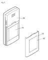
- Fig. 5 illustrates a cross-sectional view taken along line I-I of Fig. 4 ;
- Fig. 6 illustrates a perspective view of a separable battery cover having an in-mold RF antenna integrally formed therewith according to an embodiment
- Fig. 7 illustrates a sectional view of a mold for a case, in which an antenna film is disposed according to an embodiment
- Fig. 8 illustrates a sectional view of the mold of Fig. 7 with the antenna film disposed therein and into which a resin is injected.
- Fig. 1 illustrates a front perspective view of a mobile phone.
- the mobile phone may include a front case 10 and a rear case 20.
- the front case 10 may include a display window 11 occupying a wide area of the front case 10 and keypads 14 and 16 arranged in a remaining area thereof.
- the front case 10 may include a bezel 12 around a periphery of the display window 11.
- the rear case 20 may include a battery cover 22.
- Fig. 2 illustrates a rear perspective view of the mobile phone.
- the mobile phone may include the rear case 20 and the battery cover 22 separable from the rear case 20 at a rear side thereof.
- the battery cover 22 may be separated from a battery cell (not illustrated) and may be detachably mounted to the rear case 20.
- a method of an embodiment may include integrating the RF antenna with the case of a device, e.g., a mobile phone.
- the method may include disposing an RF antenna film in an injection mold for the case and then injecting a resin into the mold to form the case.
- the RF antenna When forming the RF antenna in the front case 10 of the mobile phone, the RF antenna may be integrally formed with the bezel 12 corresponding to the periphery of the display window 11. Another embodiment provides a method of integrally forming the RF antenna in the battery cover 22 to dispose the RF antenna in the rear case 20.
- Fig. 3 illustrates a flowchart of a manufacturing method for an in-mold type RF antenna according to an embodiment.
- the method may include manufacturing an antenna film in S-31.
- the manufactured antenna film may be disposed in a case mold in S-32.
- a case of a device may be formed by injecting a resin into the mold with the antenna film disposed therein in S-33.
- a copper foil may be stacked on a base film.
- An RF antenna pattern may be formed by processing, e.g., etching, the stacked copper foil.
- the base film may include, e.g., a polyimide film, a polyethylene terephthalate film, a polyphenylene sulfide film, a polyethylene naphthalate film, a polyamide film, a polycarbonate film, and/or a poly(methyl methacrylate) film.
- the antenna film may have a shape corresponding to a shape of the device.
- the antenna film When the antenna film is integrally formed with the bezel 12, i.e. around the periphery of the display window 11, the antenna film may have a frame shape.
- the antenna film when the antenna film is integrally formed with the battery cover 22, the antenna film may have a shape corresponding to a shape of the battery cover 22 and may be smaller than the battery cover.
- the battery cover 22 may be a separate cover that may be separable from a battery cell.
- the antenna film may be disposed in the mold for the case of the device.
- the antenna film may be disposed in a portion of the mold for forming, i.e., defining, an inner surface of the case.
- the case e.g., the front case 10 or battery cover 22, of the device may be injection-molded by injecting a resin into the mold.
- the antenna film may be integrally formed with the case, e.g., the front case 10 or the battery cover 22.
- an adhesive layer may be formed on a surface of the antenna film that contacts the resin.
- the adhesive layer may be disposed at an interface between the antenna film and the case resin to reinforce an attaching force between the antenna film and the resin.
- the adhesive used to reinforce the bonding force between the antenna film and the resin may include, e.g., a high temperature resistant polyester-based adhesive and/or an epoxy or phenoxy-based thermosetting adhesive.
- the adhesive may be applied to the antenna film by, e.g., roll coating, screen coating, or spray coating. The adhesive may be applied after processing the antenna film and prior to cutting the antenna film to shape or after the antenna film is disposed in the mold.
- Fig. 4 illustrates a perspective view of a front case having an in-mold type RF antenna integrally formed therewith according to an embodiment.
- Fig. 5 illustrates a cross-sectional view taken along line I-I of Fig. 4 .
- an antenna film 40 having an RF antenna may be integrally formed with the bezel 12 of the front case 10.
- the front case 10 may have a rectangular frame shape corresponding to the bezel 12 on the antenna film 40.
- the bezel 12 of the front case 10 may have an outer surface 12a exposed to the outside of the device and an inner surface 12b facing an interior of the device.
- the antenna film 40 may be integrally formed with the bezel 12 on the inner surface 12b of the bezel 12.
- the device may not provide an aesthetically pleasing appearance.
- the antenna film 40 may be formed on the inner surface 12b to ensure an aesthetically pleasing appearance of the device while also facilitating connection of the antenna film 40 to a printed circuit board.
- Fig. 6 illustrates a perspective view of a separable battery cover having an in-mold RF antenna integrally formed therewith according to another embodiment.
- a RF antenna may be integrally formed with the battery cover 22 of a mobile phone, which may have a battery cell 25 separately formed from the battery cover 22.
- an antenna film 42 having a RF antenna may be integrally formed with an inner surface of the battery cover 22.
- the battery cover 22 may remain with the mobile phone and still be used even when the battery cell 25 is replaced with new one.
- a single mobile phone set may include two battery cells (not illustrated). Therefore, if the battery cells 25 and the battery cover 22 are integrally formed with each other and RF antennae are interposed between the battery cells 25 and the battery cover 22, a number of RF antennae corresponding to the number of battery cells 25 may be required. However, as in the present embodiment, if the battery cells 25 are separated from the battery cover 22 and the RF antenna is integrally formed with the battery cover 22, a single RF antenna may be sufficient for the mobile phone, thereby reducing manufacturing costs and thus saving resources.
- Fig. 7 illustrates a sectional view of a mold for a case, in which an antenna film is disposed.
- Fig. 8 illustrates a sectional view of the mold with the antenna film disposed therein and into which a resin is injected.
- an antenna film 40 having an RF antenna pattern may be disposed in a mold for a case.
- the antenna film 40 may be formed by stacking a copper foil on a base film and processing, e.g., etching, the stacked copper foil.
- the mold may include and upper mold 62 and a lower mold 64.
- the upper mold 62 may define an outer surface of a resultant case and the lower mold 64 may define an inner surface of the resultant case.
- the antenna film 40 may be disposed not on the upper mold 62 but rather on the lower mold 64. Accordingly, the antenna film 40 may be integrally formed with the inner surface of the resultant case.
- a resin may form the case corresponding to the shape of the mold.
- the antenna film 40 may be integrally formed with the inner surface of the case.
- the RF antenna may be connected to an internal printed circuit board by, e.g., a separate soldering process or via an anisotropic conductive film (ACF). Since current may flow through the ACF only in a direction in which pressure is applied, electrical connection between portions may be obtained only by attachment of the ACF to the portions, thereby simplifying assembly.
- ACF anisotropic conductive film
- a copper foil having a thickness of 36 ⁇ m was bonded to a polyimide film (hereinafter, PI film) having a thickness of 50 ⁇ m to form a single-surface flexible copper foil plate.
- PI film polyimide film
- an antenna film was prepared by etching an RF antenna circuit in the single-surface flexible copper foil plate.
- An adhesive was coated on a rear surface of the etched flexible copper foil plate to reinforce a bonding force during injection molding.
- An RF antenna integrated case was then formed by arranging the antenna film at a predetermined position in a mold and injecting a resin into the mold.
- An antenna film was formed using the same method as in Example 1 except that a polyethylene terephthalate film (hereinafter, PET film) was used instead of using the PI film. Then, an RF antenna integrated case was formed by arranging the antenna film at a predetermined position in a mold and injecting a resin into the mold as in Example 1.
- PET film polyethylene terephthalate film
- An antenna film was formed by printing a paste consisting of 75 wt % of Ag (manufactured by DOWA) as a conductive filler, 10 wt % of bisphenol-A type epoxy resin (manufactured by Kukdo Chemical Co., Ltd) as a binder resin, 1 wt % of phthalic anhydride (manufactured by Kukdo Chemical Co., Ltd) as a curing agent, 0.5 wt % of Disper BYK (manufactured by BYK) as a dispersant and residual terpineol as a solvent having a thickness of 30 ⁇ m on a PI film having a thickness of 50 ⁇ m instead of the single-surface flexible copper foil plate of Example 1. Then, an RF antenna integrated case was formed by arranging the antenna film at a predetermined position in a mold and injecting a resin into the mold as in Example 1.
- An antenna film was formed by printing a silver (Ag) ink having a thickness of 30 ⁇ m on a PI film having a thickness of 50 ⁇ m instead of the single-surface flexible copper foil plate of Example 1. Then, an RF antenna integrated case was formed by arranging the antenna film at a predetermined position in a mold and injecting a resin into the mold as in Example 1.
- Examples 1 and 2 exhibited low circuit resistances of 0.36 ⁇ and 0.42 ⁇ , respectively.
- Examples 1 and 2 also exhibited good antenna recognition distances of 35 mm and 32 mm, respectively.
- Comparative Example 1 exhibited such high circuit resistances that the antenna recognition distance was only 5 mm. Further, the antenna of Comparative Example 2 could not be recognized at all.
- the method according to an embodiment may enhance assembly efficiency and may reduce manufacturing costs by integrally forming a RF antenna with a bezel of a display window or a separable battery cover of a case of a device.
- an RF antenna may be integrally formed with a case, thereby reducing interference between internal parts and enabling stable communications.
- an RF antenna may exhibit superior circuit resistance and antenna recognition distance.
Landscapes
- Engineering & Computer Science (AREA)
- Manufacturing & Machinery (AREA)
- Mechanical Engineering (AREA)
- Computer Networks & Wireless Communication (AREA)
- Support Of Aerials (AREA)
- Details Of Aerials (AREA)
- Injection Moulding Of Plastics Or The Like (AREA)
- Telephone Set Structure (AREA)
Abstract
Description
- The present invention relates to an in-mold type RF antenna, a device including the same, and associated methods.
- Portable devices, e.g., mobile phones, portable multimedia players (PMPs), portable digital multimedia broadcastings (DMBs), and the like, may include a display window, a battery, and at least one antenna. To perform various functions, the portable devices may include an RF antenna for recognition of radio-frequency identification (RFID) tags in addition to an antenna for transmission and reception of radio waves.
- The RF antenna may require a predetermined installation area due to size and shape requirements thereof. The RF antenna may be formed separately from a main printed circuit board and may then be attached to the main printed circuit board. The separate RF antenna may be attached to an outer case or may be integrated with a surface of a battery.
- As batteries for portable device are made thinner, interference with RFID tags may occur due to current in the battery. In addition, if the RF antenna is integrally formed with a consumable battery, an RF antenna must be integrated with all batteries for use with the portable devices. Accordingly, manufacturing costs may be increased.
- Embodiments of the invention are directed to an in-mold type RF antenna, a device including the same, and associated methods, which represent advances over the related art.
- It is an object of the invention to provide an in-mold type RF antenna with improved assembly efficiency, reduced manufacturing costs, and stable communication.
- At least one of the above and other objects and advantages may be realized by providing a method of manufacturing an in-mold type RF antenna including stacking a copper foil on a base film, forming an antenna film by processing the copper foil to form an RF antenna pattern thereon, the antenna film being configured to be accommodated in a case of a device, disposing the antenna film in a mold for forming the case of the device, and forming the case having the antenna film integrally formed therewith by injecting a resin into the mold.
- Disposing the antenna film in the mold may include disposing the antenna film in a position corresponding to a bezel surrounding a periphery of a display window of the device.
- Disposing the antenna film in the mold may include disposing the antenna film in a position corresponding to a separable battery cover of the device.
- Disposing the antenna film may include disposing the antenna film in the mold such that the antenna film is integrated with an inner surface of the case.
- The method may further include connecting the antenna film to an internal printed circuit board using an anisotropic conductive film (ACF).
- The base film may include at least one of a polyimide film, a polyethylene terephthalate film, a polyphenylene sulfide film, a polyethylene naphthalate film, a polyamide film, a polycarbonate film, and a poly(methyl methacrylate) film.
- The method may further include forming an adhesive layer on a surface of the antenna film contacting the resin.
- Forming the adhesive layer on the surface may occur prior to disposing the antenna film in the mold.
- Forming the adhesive layer on the surface may occur after disposing the antenna film in the mold.
- Forming the adhesive layer may include applying a high temperature resistant thermosetting adhesive to the surface of the antenna film by one of roll coating, screen coating, or spray coating.
- The adhesive may include at least one of a polyester-based adhesive, an epoxy-based adhesive, and a phenoxy-based adhesive.
- Processing the copper foil may include etching the copper foil.
- At least one of the above and other objects and advantages may also be realized by providing an in-mold type RF antenna manufactured by the method of an embodiment.
- At least one of the above and other objects and advantages may also be realized by providing a device including the in-mold type RF antenna of an embodiment.
- The above and other features and advantages will become more apparent to those of ordinary skill in the art by describing in detail exemplary embodiments with reference to the attached drawings, in which:
-
Fig. 1 illustrates a front perspective view of a mobile phone; -
Fig. 2 illustrates a rear perspective view of the mobile phone; -
Fig. 3 illustrates a flowchart of a method of manufacturing an in-mold type RF antenna according to an embodiment; -
Fig. 4 illustrates a perspective view of a front case having an in-mold type RF antenna integrally formed therewith according to an embodiment; -
Fig. 5 illustrates a cross-sectional view taken along line I-I ofFig. 4 ; -
Fig. 6 illustrates a perspective view of a separable battery cover having an in-mold RF antenna integrally formed therewith according to an embodiment; -
Fig. 7 illustrates a sectional view of a mold for a case, in which an antenna film is disposed according to an embodiment; and -
Fig. 8 illustrates a sectional view of the mold ofFig. 7 with the antenna film disposed therein and into which a resin is injected. - Example embodiments will now be described more fully hereinafter with reference to the accompanying drawings; however, they may be embodied in different forms and should not be construed as limited to the embodiments set forth herein. Rather, these embodiments are provided so that this disclosure will be thorough and complete, and will fully convey the scope of the invention to those skilled in the art.
- In the drawing figures, the dimensions of layers and regions may be exaggerated for clarity of illustration. It will also be understood that when a layer or element is referred to as being "on" another layer or substrate, it can be directly on the other layer or substrate, or intervening layers may also be present. In addition, it will also be understood that when a layer is referred to as being "between" two layers, it can be the only layer between the two layers, or one or more intervening layers may also be present. Like reference numerals refer to like elements throughout.
-
Fig. 1 illustrates a front perspective view of a mobile phone. Referring toFig. 1 , the mobile phone may include afront case 10 and arear case 20. Thefront case 10 may include adisplay window 11 occupying a wide area of thefront case 10 andkeypads front case 10 may include abezel 12 around a periphery of thedisplay window 11. Therear case 20 may include abattery cover 22. -
Fig. 2 illustrates a rear perspective view of the mobile phone. Referring toFig. 2 , the mobile phone may include therear case 20 and thebattery cover 22 separable from therear case 20 at a rear side thereof. Thebattery cover 22 may be separated from a battery cell (not illustrated) and may be detachably mounted to therear case 20. - A method of an embodiment may include integrating the RF antenna with the case of a device, e.g., a mobile phone. The method may include disposing an RF antenna film in an injection mold for the case and then injecting a resin into the mold to form the case.
- When forming the RF antenna in the
front case 10 of the mobile phone, the RF antenna may be integrally formed with thebezel 12 corresponding to the periphery of thedisplay window 11. Another embodiment provides a method of integrally forming the RF antenna in thebattery cover 22 to dispose the RF antenna in therear case 20. -
Fig. 3 illustrates a flowchart of a manufacturing method for an in-mold type RF antenna according to an embodiment. Referring toFig. 3 , the method may include manufacturing an antenna film in S-31. Then, the manufactured antenna film may be disposed in a case mold in S-32. Finally, a case of a device may be formed by injecting a resin into the mold with the antenna film disposed therein in S-33. - In order to manufacture the antenna film, a copper foil may be stacked on a base film. An RF antenna pattern may be formed by processing, e.g., etching, the stacked copper foil.
- The base film may include, e.g., a polyimide film, a polyethylene terephthalate film, a polyphenylene sulfide film, a polyethylene naphthalate film, a polyamide film, a polycarbonate film, and/or a poly(methyl methacrylate) film.
- The antenna film may have a shape corresponding to a shape of the device.
When the antenna film is integrally formed with thebezel 12, i.e. around the periphery of thedisplay window 11, the antenna film may have a frame shape. - On the other hand, when the antenna film is integrally formed with the
battery cover 22, the antenna film may have a shape corresponding to a shape of thebattery cover 22 and may be smaller than the battery cover. In an implementation, thebattery cover 22 may be a separate cover that may be separable from a battery cell. - After the antenna film is formed to correspond to the shape of the portion of the device case with which it will be integrated, the antenna film may be disposed in the mold for the case of the device. In an implementation, the antenna film may be disposed in a portion of the mold for forming, i.e., defining, an inner surface of the case.
- With the antenna film disposed in the mold, the case, e.g., the
front case 10 orbattery cover 22, of the device may be injection-molded by injecting a resin into the mold. As a result, the antenna film may be integrally formed with the case, e.g., thefront case 10 or thebattery cover 22. - To firmly attach the antenna film to the case of the device, an adhesive layer may be formed on a surface of the antenna film that contacts the resin. The adhesive layer may be disposed at an interface between the antenna film and the case resin to reinforce an attaching force between the antenna film and the resin. The adhesive used to reinforce the bonding force between the antenna film and the resin may include, e.g., a high temperature resistant polyester-based adhesive and/or an epoxy or phenoxy-based thermosetting adhesive. The adhesive may be applied to the antenna film by, e.g., roll coating, screen coating, or spray coating. The adhesive may be applied after processing the antenna film and prior to cutting the antenna film to shape or after the antenna film is disposed in the mold.
-
Fig. 4 illustrates a perspective view of a front case having an in-mold type RF antenna integrally formed therewith according to an embodiment.Fig. 5 illustrates a cross-sectional view taken along line I-I ofFig. 4 . - Referring to
Fig. 4 , anantenna film 40 having an RF antenna may be integrally formed with thebezel 12 of thefront case 10. Thefront case 10 may have a rectangular frame shape corresponding to thebezel 12 on theantenna film 40. - Referring to
Fig. 5 , thebezel 12 of thefront case 10 may have anouter surface 12a exposed to the outside of the device and aninner surface 12b facing an interior of the device. In an implementation, theantenna film 40 may be integrally formed with thebezel 12 on theinner surface 12b of thebezel 12. - If the
antenna film 40 is formed on theouter surface 12a of thebezel 12, the device may not provide an aesthetically pleasing appearance. Thus, theantenna film 40 may be formed on theinner surface 12b to ensure an aesthetically pleasing appearance of the device while also facilitating connection of theantenna film 40 to a printed circuit board. -
Fig. 6 illustrates a perspective view of a separable battery cover having an in-mold RF antenna integrally formed therewith according to another embodiment. Referring toFig. 6 , a RF antenna may be integrally formed with thebattery cover 22 of a mobile phone, which may have abattery cell 25 separately formed from thebattery cover 22. - In the present embodiment, an
antenna film 42 having a RF antenna may be integrally formed with an inner surface of thebattery cover 22. Thebattery cover 22 may remain with the mobile phone and still be used even when thebattery cell 25 is replaced with new one. - A single mobile phone set may include two battery cells (not illustrated). Therefore, if the
battery cells 25 and thebattery cover 22 are integrally formed with each other and RF antennae are interposed between thebattery cells 25 and thebattery cover 22, a number of RF antennae corresponding to the number ofbattery cells 25 may be required. However, as in the present embodiment, if thebattery cells 25 are separated from thebattery cover 22 and the RF antenna is integrally formed with thebattery cover 22, a single RF antenna may be sufficient for the mobile phone, thereby reducing manufacturing costs and thus saving resources. -
Fig. 7 illustrates a sectional view of a mold for a case, in which an antenna film is disposed.Fig. 8 illustrates a sectional view of the mold with the antenna film disposed therein and into which a resin is injected. - Referring to
Fig. 7 , anantenna film 40 having an RF antenna pattern may be disposed in a mold for a case. Theantenna film 40 may be formed by stacking a copper foil on a base film and processing, e.g., etching, the stacked copper foil. The mold may include andupper mold 62 and alower mold 64. Theupper mold 62 may define an outer surface of a resultant case and thelower mold 64 may define an inner surface of the resultant case. Theantenna film 40 may be disposed not on theupper mold 62 but rather on thelower mold 64. Accordingly, theantenna film 40 may be integrally formed with the inner surface of the resultant case. - Next, as illustrated in
Fig. 8 , when injected into the upper andlower molds antenna film 40 may be integrally formed with the inner surface of the case. - After the RF antenna is integrally formed with the case, the RF antenna may be connected to an internal printed circuit board by, e.g., a separate soldering process or via an anisotropic conductive film (ACF). Since current may flow through the ACF only in a direction in which pressure is applied, electrical connection between portions may be obtained only by attachment of the ACF to the portions, thereby simplifying assembly.
- A copper foil having a thickness of 36 µm was bonded to a polyimide film (hereinafter, PI film) having a thickness of 50 µm to form a single-surface flexible copper foil plate. Then, an antenna film was prepared by etching an RF antenna circuit in the single-surface flexible copper foil plate. An adhesive was coated on a rear surface of the etched flexible copper foil plate to reinforce a bonding force during injection molding. An RF antenna integrated case was then formed by arranging the antenna film at a predetermined position in a mold and injecting a resin into the mold.
- An antenna film was formed using the same method as in Example 1 except that a polyethylene terephthalate film (hereinafter, PET film) was used instead of using the PI film. Then, an RF antenna integrated case was formed by arranging the antenna film at a predetermined position in a mold and injecting a resin into the mold as in Example 1.
- An antenna film was formed by printing a paste consisting of 75 wt % of Ag (manufactured by DOWA) as a conductive filler, 10 wt % of bisphenol-A type epoxy resin (manufactured by Kukdo Chemical Co., Ltd) as a binder resin, 1 wt % of phthalic anhydride (manufactured by Kukdo Chemical Co., Ltd) as a curing agent, 0.5 wt % of Disper BYK (manufactured by BYK) as a dispersant and residual terpineol as a solvent having a thickness of 30 µm on a PI film having a thickness of 50 µm instead of the single-surface flexible copper foil plate of Example 1. Then, an RF antenna integrated case was formed by arranging the antenna film at a predetermined position in a mold and injecting a resin into the mold as in Example 1.
- An antenna film was formed by printing a silver (Ag) ink having a thickness of 30 µm on a PI film having a thickness of 50 µm instead of the single-surface flexible copper foil plate of Example 1. Then, an RF antenna integrated case was formed by arranging the antenna film at a predetermined position in a mold and injecting a resin into the mold as in Example 1.
- The materials for the base films and circuit patterns of the Examples and Comparative Examples are shown in Table 1.
Table 1 Classification Example 1 Example 2 Comparative Example 1 Comparative Example 2 Material of base film PI film PET film PI film PET film Material of circuit pattern Copper foil Copper foil Paste Ag ink - Circuit resistances, deformation after injection molding, and antenna recognition distances of the RF antenna integrated cases manufactured as described above were measured. The results are shown in Table 2.
Table 2 Classification Example 1 Example 2 Comparative Example 1 Comparative Example 2 Circuit resistance (Ω) 0.36 0.42 1.16 2.05 Deformation after injection molding None None None None Antenna recognition distance 35 mm 32 mm 5 mm Not recognized - According to the results, no deformation after injection molding was observed in any of Examples 1 and 2 and Comparative Examples 1 and 2. Examples 1 and 2 exhibited low circuit resistances of 0.36 Ω and 0.42 Ω, respectively. Examples 1 and 2 also exhibited good antenna recognition distances of 35 mm and 32 mm, respectively.
- In contrast, Comparative Example 1 exhibited such high circuit resistances that the antenna recognition distance was only 5 mm. Further, the antenna of Comparative Example 2 could not be recognized at all.
- As apparent from the above description, the method according to an embodiment may enhance assembly efficiency and may reduce manufacturing costs by integrally forming a RF antenna with a bezel of a display window or a separable battery cover of a case of a device.
- Further, according to an embodiment, an RF antenna may be integrally formed with a case, thereby reducing interference between internal parts and enabling stable communications.
- In addition, according to an embodiment, an RF antenna may exhibit superior circuit resistance and antenna recognition distance.
- Exemplary embodiments have been disclosed herein, and although specific terms are employed, they are used and are to be interpreted in a generic and descriptive sense only and not for purpose of limitation.
- Korean Patent Application No.
10-2009-0010642, filed on February 10, 2009
Claims (14)
- A method of manufacturing an in-mold type RF antenna, comprising:stacking a copper foil on a base film;forming an antenna film by processing the copper foil to form an RF antenna pattern thereon, the antenna film being configured to be accommodated in a case of a device;disposing the antenna film in a mold for forming the case of the device; andforming the case having the antenna film integrally formed therewith by injecting a resin into the mold.
- The method as claimed in claim 1, wherein disposing the antenna film in the mold includes disposing the antenna film in a position corresponding to a bezel surrounding a periphery of a display window of the device.
- The method as claimed in claim 1, wherein disposing the antenna film in the mold includes disposing the antenna film in a position corresponding to a separable battery cover of the device.
- The method as claimed in any of claims 1 to 3, wherein disposing the antenna film includes disposing the antenna film in the mold such that the antenna film is integrated with an inner surface of the case.
- The method as claimed in any of claims 1 to 4, further comprising:connecting the antenna film to an internal printed circuit board using an anisotropic conductive film (ACF).
- The method as claimed in any of claims 2 to 5, wherein the base film includes at least one of a polyimide film, a polyethylene terephthalate film, a polyphenylene sulfide film, a polyethylene naphthalate film, a polyamide film, a polycarbonate film, and a poly(methyl methacrylate) film.
- The method as claimed in any of claims 1 to 6, further comprising:forming an adhesive layer on a surface of the antenna film contacting the resin.
- The method as claimed in claim 7, wherein forming the adhesive layer on the surface occurs prior to disposing the antenna film in the mold.
- The method as claimed in claim 7, wherein forming the adhesive layer on the surface occurs after disposing the antenna film in the mold.
- The method as claimed in any one of claims 7 to 9, wherein forming the adhesive layer includes applying a high temperature resistant thermosetting adhesive to the surface of the antenna film by one of roll coating, screen coating, or spray coating.
- The method as claimed in claim 10, wherein the adhesive includes at least one of a polyester-based adhesive, an epoxy-based adhesive, and a phenoxy-based adhesive.
- The method as claimed in any of claims 1 to 11, wherein processing the copper foil includes etching the copper foil.
- An in-mold type RF antenna obtainable by performing the method as claimed in any of claims 1 to 12.
- A device including the in-mold type RF antenna of claim 13.
Priority Applications (1)
| Application Number | Priority Date | Filing Date | Title |
|---|---|---|---|
| EP11161493A EP2353834A1 (en) | 2009-02-10 | 2010-02-10 | In-mold type RF antenna, device including the same, and associated methods |
Applications Claiming Priority (1)
| Application Number | Priority Date | Filing Date | Title |
|---|---|---|---|
| KR1020090010642A KR101127101B1 (en) | 2009-02-10 | 2009-02-10 | In-mold type roof antena and it's manufacturing method |
Related Child Applications (1)
| Application Number | Title | Priority Date | Filing Date |
|---|---|---|---|
| EP11161493.9 Division-Into | 2011-04-07 |
Publications (3)
| Publication Number | Publication Date |
|---|---|
| EP2223789A2 true EP2223789A2 (en) | 2010-09-01 |
| EP2223789A3 EP2223789A3 (en) | 2010-10-27 |
| EP2223789B1 EP2223789B1 (en) | 2013-04-10 |
Family
ID=42173319
Family Applications (2)
| Application Number | Title | Priority Date | Filing Date |
|---|---|---|---|
| EP11161493A Withdrawn EP2353834A1 (en) | 2009-02-10 | 2010-02-10 | In-mold type RF antenna, device including the same, and associated methods |
| EP10153183.8A Not-in-force EP2223789B1 (en) | 2009-02-10 | 2010-02-10 | In-mold type RF antenna, device including the same, and associated methods |
Family Applications Before (1)
| Application Number | Title | Priority Date | Filing Date |
|---|---|---|---|
| EP11161493A Withdrawn EP2353834A1 (en) | 2009-02-10 | 2010-02-10 | In-mold type RF antenna, device including the same, and associated methods |
Country Status (5)
| Country | Link |
|---|---|
| US (1) | US8400363B2 (en) |
| EP (2) | EP2353834A1 (en) |
| JP (1) | JP2010187361A (en) |
| KR (1) | KR101127101B1 (en) |
| CN (1) | CN101826654B (en) |
Cited By (2)
| Publication number | Priority date | Publication date | Assignee | Title |
|---|---|---|---|---|
| WO2021148137A1 (en) * | 2020-01-24 | 2021-07-29 | Huawei Technologies Co., Ltd. | Functional housing structure for an electronic device |
| US12249753B2 (en) | 2022-03-16 | 2025-03-11 | Honeywell International Inc. | Osprey migratory 7-band LTE and ISM antenna |
Families Citing this family (13)
| Publication number | Priority date | Publication date | Assignee | Title |
|---|---|---|---|---|
| US8766858B2 (en) * | 2010-08-27 | 2014-07-01 | Apple Inc. | Antennas mounted under dielectric plates |
| CN102049838A (en) * | 2010-11-09 | 2011-05-11 | 深圳庆和胶粘制品有限公司 | Method for molding metal piece with view window and plastic molding product and application thereof |
| US8760349B2 (en) | 2010-11-26 | 2014-06-24 | Intel Corporation | Method and apparatus for in-mold laminate antennas |
| KR101157598B1 (en) * | 2011-02-21 | 2012-06-19 | 주식회사 에이티앤씨 | Method for manufacturing case of mobile device with antenna |
| JP2012195647A (en) * | 2011-03-15 | 2012-10-11 | Alps Electric Co Ltd | Antenna structure and portable communication terminal |
| US9246219B2 (en) * | 2011-07-07 | 2016-01-26 | Htc Corporation | Handheld device |
| WO2013051400A1 (en) | 2011-10-03 | 2013-04-11 | 株式会社村田製作所 | Ultrasonic-wave generation device |
| KR101409399B1 (en) * | 2012-01-13 | 2014-06-23 | 주식회사 알.에프.텍 | Method of Manufacturing a Case of Mobile Electronic Apparatus with Antenna |
| CN104137569B (en) | 2012-02-23 | 2017-05-24 | 株式会社村田制作所 | Ultrasonic wave-generating device |
| KR101975262B1 (en) * | 2012-05-31 | 2019-09-09 | 삼성전자주식회사 | Cover having metal grid structure and method for forming thereof |
| KR101973127B1 (en) | 2012-11-13 | 2019-04-26 | 삼성전자주식회사 | Antenna apparatus for portable terminal |
| KR102500480B1 (en) * | 2017-12-22 | 2023-02-16 | 삼성전자주식회사 | Electronic device including contact member and manufacturing method of the same |
| CN108428830A (en) * | 2018-03-06 | 2018-08-21 | 维沃移动通信有限公司 | A kind of preparation method of battery cover, battery cover and mobile terminal |
Citations (1)
| Publication number | Priority date | Publication date | Assignee | Title |
|---|---|---|---|---|
| US20080150813A1 (en) | 2006-07-26 | 2008-06-26 | Acer Incorporated | Electronic Apparatus with an Antenna |
Family Cites Families (26)
| Publication number | Priority date | Publication date | Assignee | Title |
|---|---|---|---|---|
| CA2021887A1 (en) | 1989-07-26 | 1991-01-27 | Shigeru Nedzu | Polyalkylene terephthalate resin molded article having pictorial pattern formed thereon and process for preparation thereof |
| EP0543664A3 (en) | 1991-11-21 | 1993-09-22 | Nifco Inc. | Parabolic antenna and method of manufacturing reflector body of the same |
| AU9657998A (en) | 1997-10-28 | 1999-05-17 | Telefonaktiebolaget Lm Ericsson (Publ) | Multiple band, multiple branch antenna for mobile phone |
| DE60135100D1 (en) * | 2000-03-24 | 2008-09-11 | Cymbet Corp | E WITH ULTRA-THIN ELECTROLYTES |
| JP2003158415A (en) * | 2001-11-20 | 2003-05-30 | Ntn Corp | Equipment with radio communication function |
| US6600450B1 (en) * | 2002-03-05 | 2003-07-29 | Motorola, Inc. | Balanced multi-band antenna system |
| US6677906B2 (en) * | 2002-04-17 | 2004-01-13 | Dell Products L.P. | Glass antenna for laptop computers |
| US7367114B2 (en) * | 2002-08-26 | 2008-05-06 | Littelfuse, Inc. | Method for plasma etching to manufacture electrical devices having circuit protection |
| AU2002340506A1 (en) * | 2002-11-07 | 2004-06-07 | Fractus, S.A. | Integrated circuit package including miniature antenna |
| ATE551780T1 (en) * | 2003-07-23 | 2012-04-15 | Lg Electronics Inc | INTERNAL ANTENNA AND A MOBILE DEVICE WITH THIS INTERNAL ANTENNA |
| JP4067510B2 (en) * | 2004-03-31 | 2008-03-26 | シャープ株式会社 | Television receiver |
| KR100606820B1 (en) * | 2004-05-11 | 2006-08-01 | 엘지전자 주식회사 | Battery cover, battery pack and manufacturing method of mobile communication terminal |
| JP2005333244A (en) * | 2004-05-18 | 2005-12-02 | Mitsubishi Electric Corp | Mobile phone |
| TWI265431B (en) * | 2004-09-07 | 2006-11-01 | Acer Inc | Notebook computer with antenna array module |
| WO2006043543A1 (en) | 2004-10-18 | 2006-04-27 | Matsushita Electric Industrial Co., Ltd. | Noncontact communication antenna and portable mobile terminal |
| US8178958B2 (en) * | 2004-10-19 | 2012-05-15 | Semiconductor Energy Laboratory Co., Ltd. | Semiconductor device having antenna and method for manufacturing thereof |
| JP4815894B2 (en) * | 2005-06-27 | 2011-11-16 | セントラル硝子株式会社 | Method for manufacturing window glass with decorative molding and window glass with decorative molding |
| JP4367552B2 (en) * | 2006-01-19 | 2009-11-18 | 株式会社村田製作所 | Wireless IC device |
| JP4783194B2 (en) * | 2006-04-11 | 2011-09-28 | 富士通コンポーネント株式会社 | Portable device |
| JP2007311955A (en) * | 2006-05-17 | 2007-11-29 | Dainippon Printing Co Ltd | Non-contact IC tag having a back metal layer |
| KR20070118328A (en) | 2006-06-12 | 2007-12-17 | 권남홍 | Built-in antenna manufacturing method |
| DE102007043409A1 (en) * | 2006-09-15 | 2008-03-27 | Samsung Electro-Mechanics Co., Ltd., Suwon | Method for producing a housing structure with antenna |
| KR100840514B1 (en) | 2006-10-10 | 2008-06-23 | 주식회사 이엠따블유안테나 | Antenna module, formation method thereof and wireless communication terminal including same |
| DE102007049284A1 (en) | 2007-10-12 | 2009-04-16 | Benteler Automobiltechnik Gmbh | Method for manufacturing metal or plastic components, particularly vehicle components, particularly undercarriage components in vehicle construction, involves dividing metal part of plate or strip material to be converted into saucer shape |
| CN101500381A (en) | 2008-01-30 | 2009-08-05 | 深圳富泰宏精密工业有限公司 | Housing, manufacturing method for the housing and electronic apparatus applying the housing |
| KR100979893B1 (en) * | 2008-08-06 | 2010-09-03 | 주식회사 이엠따블유 | Built-in antenna of wireless device and manufacturing method thereof |
-
2009
- 2009-02-10 KR KR1020090010642A patent/KR101127101B1/en not_active Expired - Fee Related
- 2009-10-19 JP JP2009240395A patent/JP2010187361A/en active Pending
-
2010
- 2010-01-07 US US12/654,875 patent/US8400363B2/en not_active Expired - Fee Related
- 2010-02-08 CN CN201010112252.5A patent/CN101826654B/en not_active Expired - Fee Related
- 2010-02-10 EP EP11161493A patent/EP2353834A1/en not_active Withdrawn
- 2010-02-10 EP EP10153183.8A patent/EP2223789B1/en not_active Not-in-force
Patent Citations (1)
| Publication number | Priority date | Publication date | Assignee | Title |
|---|---|---|---|---|
| US20080150813A1 (en) | 2006-07-26 | 2008-06-26 | Acer Incorporated | Electronic Apparatus with an Antenna |
Cited By (2)
| Publication number | Priority date | Publication date | Assignee | Title |
|---|---|---|---|---|
| WO2021148137A1 (en) * | 2020-01-24 | 2021-07-29 | Huawei Technologies Co., Ltd. | Functional housing structure for an electronic device |
| US12249753B2 (en) | 2022-03-16 | 2025-03-11 | Honeywell International Inc. | Osprey migratory 7-band LTE and ISM antenna |
Also Published As
| Publication number | Publication date |
|---|---|
| US20100201582A1 (en) | 2010-08-12 |
| JP2010187361A (en) | 2010-08-26 |
| EP2353834A1 (en) | 2011-08-10 |
| KR20100091452A (en) | 2010-08-19 |
| KR101127101B1 (en) | 2012-03-23 |
| CN101826654B (en) | 2014-03-26 |
| CN101826654A (en) | 2010-09-08 |
| US8400363B2 (en) | 2013-03-19 |
| EP2223789A3 (en) | 2010-10-27 |
| EP2223789B1 (en) | 2013-04-10 |
Similar Documents
| Publication | Publication Date | Title |
|---|---|---|
| EP2223789B1 (en) | In-mold type RF antenna, device including the same, and associated methods | |
| CN102668236B (en) | Mobile device | |
| US8203491B2 (en) | Housing, wireless communication device using the housing, and manufacturing method thereof | |
| US8711041B2 (en) | Case of electronic device having antenna pattern embedded therein and mold and method for manufacturing the same | |
| US9266266B2 (en) | Case of electronic device having antenna pattern frame embedded therein, mold therefor and method of manufacturing thereof | |
| US20070257398A1 (en) | Laminated electronic components for insert molding | |
| US7742312B2 (en) | Electronic device and method of fabrication of a same | |
| EP2387106B1 (en) | Case of electronic device having low frequency antenna pattern embedded therein, mold therefor and method of manufacturing thereof | |
| US20110304517A1 (en) | Housing of portable electronic device and method for making the same | |
| US20090289856A1 (en) | Film type antenna and mobile communication terminal | |
| KR20100003035A (en) | Film type antenna and mobile communication terminal comprising the same | |
| US8154458B2 (en) | Antenna module, method for making the antenna module, and housing incorporating the antenna module | |
| US20110304511A1 (en) | Housing of portable electronic device and method for making the same | |
| WO2010120062A2 (en) | Method for manufacturing an antenna using a conductive material, and antenna manufactured by the method | |
| CN101752658B (en) | Antenna assembly, method for manufacturing antenna assembly and shell integrated with antenna assembly | |
| US20090213017A1 (en) | Housing, wireless communication device using the housing, and manufacturing method thereof | |
| KR101486473B1 (en) | Method for manufacturing in-mold antenna | |
| KR101971108B1 (en) | Antenna module and method of manufacturing the same | |
| KR100992520B1 (en) | Method of mounting of a insert mold antenna using dual injection molding | |
| Manabu | Reduced electrical resistance of antennae and wiring |
Legal Events
| Date | Code | Title | Description |
|---|---|---|---|
| PUAI | Public reference made under article 153(3) epc to a published international application that has entered the european phase |
Free format text: ORIGINAL CODE: 0009012 |
|
| 17P | Request for examination filed |
Effective date: 20100210 |
|
| AK | Designated contracting states |
Kind code of ref document: A2 Designated state(s): AT BE BG CH CY CZ DE DK EE ES FI FR GB GR HR HU IE IS IT LI LT LU LV MC MK MT NL NO PL PT RO SE SI SK SM TR |
|
| AX | Request for extension of the european patent |
Extension state: AL BA RS |
|
| PUAL | Search report despatched |
Free format text: ORIGINAL CODE: 0009013 |
|
| AK | Designated contracting states |
Kind code of ref document: A3 Designated state(s): AT BE BG CH CY CZ DE DK EE ES FI FR GB GR HR HU IE IS IT LI LT LU LV MC MK MT NL NO PL PT RO SE SI SK SM TR |
|
| AX | Request for extension of the european patent |
Extension state: AL BA RS |
|
| 17Q | First examination report despatched |
Effective date: 20110609 |
|
| GRAP | Despatch of communication of intention to grant a patent |
Free format text: ORIGINAL CODE: EPIDOSNIGR1 |
|
| GRAS | Grant fee paid |
Free format text: ORIGINAL CODE: EPIDOSNIGR3 |
|
| GRAA | (expected) grant |
Free format text: ORIGINAL CODE: 0009210 |
|
| AK | Designated contracting states |
Kind code of ref document: B1 Designated state(s): AT BE BG CH CY CZ DE DK EE ES FI FR GB GR HR HU IE IS IT LI LT LU LV MC MK MT NL NO PL PT RO SE SI SK SM TR |
|
| REG | Reference to a national code |
Ref country code: GB Ref legal event code: FG4D |
|
| REG | Reference to a national code |
Ref country code: CH Ref legal event code: EP Ref country code: AT Ref legal event code: REF Ref document number: 605729 Country of ref document: AT Kind code of ref document: T Effective date: 20130415 |
|
| REG | Reference to a national code |
Ref country code: IE Ref legal event code: FG4D |
|
| REG | Reference to a national code |
Ref country code: DE Ref legal event code: R096 Ref document number: 602010006136 Country of ref document: DE Effective date: 20130606 |
|
| REG | Reference to a national code |
Ref country code: DE Ref legal event code: R082 Ref document number: 602010006136 Country of ref document: DE Representative=s name: BARDEHLE PAGENBERG PARTNERSCHAFT PATENTANWAELT, DE Ref country code: DE Ref legal event code: R082 Ref document number: 602010006136 Country of ref document: DE Representative=s name: BARDEHLE PAGENBERG PARTNERSCHAFT MBB PATENTANW, DE |
|
| PG25 | Lapsed in a contracting state [announced via postgrant information from national office to epo] |
Ref country code: SI Free format text: LAPSE BECAUSE OF FAILURE TO SUBMIT A TRANSLATION OF THE DESCRIPTION OR TO PAY THE FEE WITHIN THE PRESCRIBED TIME-LIMIT Effective date: 20130410 |
|
| REG | Reference to a national code |
Ref country code: NL Ref legal event code: T3 |
|
| REG | Reference to a national code |
Ref country code: AT Ref legal event code: MK05 Ref document number: 605729 Country of ref document: AT Kind code of ref document: T Effective date: 20130410 |
|
| REG | Reference to a national code |
Ref country code: LT Ref legal event code: MG4D |
|
| PG25 | Lapsed in a contracting state [announced via postgrant information from national office to epo] |
Ref country code: FI Free format text: LAPSE BECAUSE OF FAILURE TO SUBMIT A TRANSLATION OF THE DESCRIPTION OR TO PAY THE FEE WITHIN THE PRESCRIBED TIME-LIMIT Effective date: 20130410 Ref country code: AT Free format text: LAPSE BECAUSE OF FAILURE TO SUBMIT A TRANSLATION OF THE DESCRIPTION OR TO PAY THE FEE WITHIN THE PRESCRIBED TIME-LIMIT Effective date: 20130410 Ref country code: ES Free format text: LAPSE BECAUSE OF FAILURE TO SUBMIT A TRANSLATION OF THE DESCRIPTION OR TO PAY THE FEE WITHIN THE PRESCRIBED TIME-LIMIT Effective date: 20130721 Ref country code: GR Free format text: LAPSE BECAUSE OF FAILURE TO SUBMIT A TRANSLATION OF THE DESCRIPTION OR TO PAY THE FEE WITHIN THE PRESCRIBED TIME-LIMIT Effective date: 20130711 Ref country code: NO Free format text: LAPSE BECAUSE OF FAILURE TO SUBMIT A TRANSLATION OF THE DESCRIPTION OR TO PAY THE FEE WITHIN THE PRESCRIBED TIME-LIMIT Effective date: 20130710 Ref country code: IS Free format text: LAPSE BECAUSE OF FAILURE TO SUBMIT A TRANSLATION OF THE DESCRIPTION OR TO PAY THE FEE WITHIN THE PRESCRIBED TIME-LIMIT Effective date: 20130810 Ref country code: SE Free format text: LAPSE BECAUSE OF FAILURE TO SUBMIT A TRANSLATION OF THE DESCRIPTION OR TO PAY THE FEE WITHIN THE PRESCRIBED TIME-LIMIT Effective date: 20130410 Ref country code: LT Free format text: LAPSE BECAUSE OF FAILURE TO SUBMIT A TRANSLATION OF THE DESCRIPTION OR TO PAY THE FEE WITHIN THE PRESCRIBED TIME-LIMIT Effective date: 20130410 Ref country code: PT Free format text: LAPSE BECAUSE OF FAILURE TO SUBMIT A TRANSLATION OF THE DESCRIPTION OR TO PAY THE FEE WITHIN THE PRESCRIBED TIME-LIMIT Effective date: 20130812 Ref country code: BE Free format text: LAPSE BECAUSE OF FAILURE TO SUBMIT A TRANSLATION OF THE DESCRIPTION OR TO PAY THE FEE WITHIN THE PRESCRIBED TIME-LIMIT Effective date: 20130410 |
|
| PG25 | Lapsed in a contracting state [announced via postgrant information from national office to epo] |
Ref country code: PL Free format text: LAPSE BECAUSE OF FAILURE TO SUBMIT A TRANSLATION OF THE DESCRIPTION OR TO PAY THE FEE WITHIN THE PRESCRIBED TIME-LIMIT Effective date: 20130410 Ref country code: BG Free format text: LAPSE BECAUSE OF FAILURE TO SUBMIT A TRANSLATION OF THE DESCRIPTION OR TO PAY THE FEE WITHIN THE PRESCRIBED TIME-LIMIT Effective date: 20130710 Ref country code: LV Free format text: LAPSE BECAUSE OF FAILURE TO SUBMIT A TRANSLATION OF THE DESCRIPTION OR TO PAY THE FEE WITHIN THE PRESCRIBED TIME-LIMIT Effective date: 20130410 Ref country code: CY Free format text: LAPSE BECAUSE OF FAILURE TO SUBMIT A TRANSLATION OF THE DESCRIPTION OR TO PAY THE FEE WITHIN THE PRESCRIBED TIME-LIMIT Effective date: 20130410 Ref country code: HR Free format text: LAPSE BECAUSE OF FAILURE TO SUBMIT A TRANSLATION OF THE DESCRIPTION OR TO PAY THE FEE WITHIN THE PRESCRIBED TIME-LIMIT Effective date: 20130410 |
|
| PG25 | Lapsed in a contracting state [announced via postgrant information from national office to epo] |
Ref country code: EE Free format text: LAPSE BECAUSE OF FAILURE TO SUBMIT A TRANSLATION OF THE DESCRIPTION OR TO PAY THE FEE WITHIN THE PRESCRIBED TIME-LIMIT Effective date: 20130410 Ref country code: DK Free format text: LAPSE BECAUSE OF FAILURE TO SUBMIT A TRANSLATION OF THE DESCRIPTION OR TO PAY THE FEE WITHIN THE PRESCRIBED TIME-LIMIT Effective date: 20130410 Ref country code: CZ Free format text: LAPSE BECAUSE OF FAILURE TO SUBMIT A TRANSLATION OF THE DESCRIPTION OR TO PAY THE FEE WITHIN THE PRESCRIBED TIME-LIMIT Effective date: 20130410 Ref country code: SK Free format text: LAPSE BECAUSE OF FAILURE TO SUBMIT A TRANSLATION OF THE DESCRIPTION OR TO PAY THE FEE WITHIN THE PRESCRIBED TIME-LIMIT Effective date: 20130410 |
|
| PLBE | No opposition filed within time limit |
Free format text: ORIGINAL CODE: 0009261 |
|
| STAA | Information on the status of an ep patent application or granted ep patent |
Free format text: STATUS: NO OPPOSITION FILED WITHIN TIME LIMIT |
|
| PG25 | Lapsed in a contracting state [announced via postgrant information from national office to epo] |
Ref country code: IT Free format text: LAPSE BECAUSE OF FAILURE TO SUBMIT A TRANSLATION OF THE DESCRIPTION OR TO PAY THE FEE WITHIN THE PRESCRIBED TIME-LIMIT Effective date: 20130410 Ref country code: RO Free format text: LAPSE BECAUSE OF FAILURE TO SUBMIT A TRANSLATION OF THE DESCRIPTION OR TO PAY THE FEE WITHIN THE PRESCRIBED TIME-LIMIT Effective date: 20130410 |
|
| 26N | No opposition filed |
Effective date: 20140113 |
|
| REG | Reference to a national code |
Ref country code: DE Ref legal event code: R097 Ref document number: 602010006136 Country of ref document: DE Effective date: 20140113 |
|
| PG25 | Lapsed in a contracting state [announced via postgrant information from national office to epo] |
Ref country code: LU Free format text: LAPSE BECAUSE OF FAILURE TO SUBMIT A TRANSLATION OF THE DESCRIPTION OR TO PAY THE FEE WITHIN THE PRESCRIBED TIME-LIMIT Effective date: 20140210 Ref country code: MC Free format text: LAPSE BECAUSE OF FAILURE TO SUBMIT A TRANSLATION OF THE DESCRIPTION OR TO PAY THE FEE WITHIN THE PRESCRIBED TIME-LIMIT Effective date: 20130410 |
|
| REG | Reference to a national code |
Ref country code: CH Ref legal event code: PL |
|
| GBPC | Gb: european patent ceased through non-payment of renewal fee |
Effective date: 20140210 |
|
| PG25 | Lapsed in a contracting state [announced via postgrant information from national office to epo] |
Ref country code: CH Free format text: LAPSE BECAUSE OF NON-PAYMENT OF DUE FEES Effective date: 20140228 Ref country code: LI Free format text: LAPSE BECAUSE OF NON-PAYMENT OF DUE FEES Effective date: 20140228 |
|
| REG | Reference to a national code |
Ref country code: FR Ref legal event code: ST Effective date: 20141031 |
|
| REG | Reference to a national code |
Ref country code: IE Ref legal event code: MM4A |
|
| PG25 | Lapsed in a contracting state [announced via postgrant information from national office to epo] |
Ref country code: IE Free format text: LAPSE BECAUSE OF NON-PAYMENT OF DUE FEES Effective date: 20140210 Ref country code: FR Free format text: LAPSE BECAUSE OF NON-PAYMENT OF DUE FEES Effective date: 20140228 Ref country code: GB Free format text: LAPSE BECAUSE OF NON-PAYMENT OF DUE FEES Effective date: 20140210 |
|
| PG25 | Lapsed in a contracting state [announced via postgrant information from national office to epo] |
Ref country code: MT Free format text: LAPSE BECAUSE OF FAILURE TO SUBMIT A TRANSLATION OF THE DESCRIPTION OR TO PAY THE FEE WITHIN THE PRESCRIBED TIME-LIMIT Effective date: 20130410 |
|
| PG25 | Lapsed in a contracting state [announced via postgrant information from national office to epo] |
Ref country code: SM Free format text: LAPSE BECAUSE OF FAILURE TO SUBMIT A TRANSLATION OF THE DESCRIPTION OR TO PAY THE FEE WITHIN THE PRESCRIBED TIME-LIMIT Effective date: 20130410 |
|
| PG25 | Lapsed in a contracting state [announced via postgrant information from national office to epo] |
Ref country code: HU Free format text: LAPSE BECAUSE OF FAILURE TO SUBMIT A TRANSLATION OF THE DESCRIPTION OR TO PAY THE FEE WITHIN THE PRESCRIBED TIME-LIMIT; INVALID AB INITIO Effective date: 20100210 Ref country code: TR Free format text: LAPSE BECAUSE OF FAILURE TO SUBMIT A TRANSLATION OF THE DESCRIPTION OR TO PAY THE FEE WITHIN THE PRESCRIBED TIME-LIMIT Effective date: 20130410 |
|
| REG | Reference to a national code |
Ref country code: NL Ref legal event code: PD Owner name: LOTTE ADVANCED MATERIALS CO., LTD.; KR Free format text: DETAILS ASSIGNMENT: CHANGE OF OWNER(S), MERGE; FORMER OWNER NAME: SAMSUNG SDI CO., LTD. Effective date: 20170221 |
|
| REG | Reference to a national code |
Ref country code: DE Ref legal event code: R081 Ref document number: 602010006136 Country of ref document: DE Owner name: LOTTE ADVANCED MATERIALS CO., LTD., YEOSU-SI, KR Free format text: FORMER OWNER: CHEIL INDUSTRIES INC., GUMI-SI, GYEONGSANGBUK-DO, KR Ref country code: DE Ref legal event code: R082 Ref document number: 602010006136 Country of ref document: DE Representative=s name: BARDEHLE PAGENBERG PARTNERSCHAFT MBB PATENTANW, DE |
|
| REG | Reference to a national code |
Ref country code: DE Ref legal event code: R081 Ref document number: 602010006136 Country of ref document: DE Owner name: LOTTE ADVANCED MATERIALS CO., LTD., YEOSU-SI, KR Free format text: FORMER OWNER: SAMSUNG SDI CO., LTD., YONGIN-SI, KYONGGI-DO, KR Ref country code: DE Ref legal event code: R082 Ref document number: 602010006136 Country of ref document: DE Representative=s name: BARDEHLE PAGENBERG PARTNERSCHAFT MBB PATENTANW, DE |
|
| PG25 | Lapsed in a contracting state [announced via postgrant information from national office to epo] |
Ref country code: MK Free format text: LAPSE BECAUSE OF FAILURE TO SUBMIT A TRANSLATION OF THE DESCRIPTION OR TO PAY THE FEE WITHIN THE PRESCRIBED TIME-LIMIT Effective date: 20130410 |
|
| PGFP | Annual fee paid to national office [announced via postgrant information from national office to epo] |
Ref country code: DE Payment date: 20220105 Year of fee payment: 13 |
|
| PGFP | Annual fee paid to national office [announced via postgrant information from national office to epo] |
Ref country code: NL Payment date: 20220118 Year of fee payment: 13 |
|
| REG | Reference to a national code |
Ref country code: DE Ref legal event code: R119 Ref document number: 602010006136 Country of ref document: DE |
|
| REG | Reference to a national code |
Ref country code: NL Ref legal event code: MM Effective date: 20230301 |
|
| PG25 | Lapsed in a contracting state [announced via postgrant information from national office to epo] |
Ref country code: NL Free format text: LAPSE BECAUSE OF NON-PAYMENT OF DUE FEES Effective date: 20230301 |
|
| PG25 | Lapsed in a contracting state [announced via postgrant information from national office to epo] |
Ref country code: DE Free format text: LAPSE BECAUSE OF NON-PAYMENT OF DUE FEES Effective date: 20230901 |