EP2221967A1 - High frequency apparatus - Google Patents
High frequency apparatus Download PDFInfo
- Publication number
- EP2221967A1 EP2221967A1 EP10153948A EP10153948A EP2221967A1 EP 2221967 A1 EP2221967 A1 EP 2221967A1 EP 10153948 A EP10153948 A EP 10153948A EP 10153948 A EP10153948 A EP 10153948A EP 2221967 A1 EP2221967 A1 EP 2221967A1
- Authority
- EP
- European Patent Office
- Prior art keywords
- high frequency
- circuit
- switch
- terminal
- saw filter
- Prior art date
- Legal status (The legal status is an assumption and is not a legal conclusion. Google has not performed a legal analysis and makes no representation as to the accuracy of the status listed.)
- Withdrawn
Links
- 238000010897 surface acoustic wave method Methods 0.000 description 109
- 238000010586 diagram Methods 0.000 description 14
- 230000005283 ground state Effects 0.000 description 13
- 239000003990 capacitor Substances 0.000 description 4
- 230000004048 modification Effects 0.000 description 4
- 238000012986 modification Methods 0.000 description 4
- 230000008901 benefit Effects 0.000 description 2
- 230000005540 biological transmission Effects 0.000 description 2
- 230000006872 improvement Effects 0.000 description 2
- 230000010355 oscillation Effects 0.000 description 2
- 238000005476 soldering Methods 0.000 description 2
- 206010048669 Terminal state Diseases 0.000 description 1
- 230000004075 alteration Effects 0.000 description 1
- 230000003321 amplification Effects 0.000 description 1
- 238000003199 nucleic acid amplification method Methods 0.000 description 1
- 230000004044 response Effects 0.000 description 1
- 230000005236 sound signal Effects 0.000 description 1
Images



Classifications
-
- H—ELECTRICITY
- H03—ELECTRONIC CIRCUITRY
- H03J—TUNING RESONANT CIRCUITS; SELECTING RESONANT CIRCUITS
- H03J5/00—Discontinuous tuning; Selecting predetermined frequencies; Selecting frequency bands with or without continuous tuning in one or more of the bands, e.g. push-button tuning, turret tuner
- H03J5/24—Discontinuous tuning; Selecting predetermined frequencies; Selecting frequency bands with or without continuous tuning in one or more of the bands, e.g. push-button tuning, turret tuner with a number of separate pretuned tuning circuits or separate tuning elements selectively brought into circuit, e.g. for waveband selection or for television channel selection
- H03J5/242—Discontinuous tuning; Selecting predetermined frequencies; Selecting frequency bands with or without continuous tuning in one or more of the bands, e.g. push-button tuning, turret tuner with a number of separate pretuned tuning circuits or separate tuning elements selectively brought into circuit, e.g. for waveband selection or for television channel selection used exclusively for band selection
- H03J5/244—Discontinuous tuning; Selecting predetermined frequencies; Selecting frequency bands with or without continuous tuning in one or more of the bands, e.g. push-button tuning, turret tuner with a number of separate pretuned tuning circuits or separate tuning elements selectively brought into circuit, e.g. for waveband selection or for television channel selection used exclusively for band selection using electronic means
Definitions
- the present invention relates to a high frequency apparatus capable of performing a band switching operation by switching a terminal connection state of a SAW filter input section.
- a SAW (Surface Acoustic Wave) filter is connected to a rear-stage of an intermediate frequency signal amplification circuit that amplifies an intermediate frequency signal supplied from a tuner.
- a television receiver capable of receiving both terrestrial digital broadcasting and analog broadcasting is provided with a digital SAW filter compatible with a digital broadcasting signal and an analog SAW filter compatible with an analog broadcasting signal.
- the television broadcasting schemes of each country include PAL/B schemes, PAL/G schemes, PAL/D schemes, PAL/K schemes, NTSC/M schemes, NTSC/N schemes, SECAM/L schemes and the like.
- SECAM/L scheme employed in France in relation to four channels treated as a VHF low band, frequencies of an image signal carrier and a sound signal carrier are inverted to each other as compared with those in other VHF low band channels, VHF high band channels and UHF channels.
- a SAW filter for an image is provided separately from a SAW filter for sound. Further, the SAW filter for sound is configured to switch a band according to the SECAM/L scheme.
- Fig. 6 is a diagram illustrating the configuration of the television receiver compatible with an analog scheme and a digital scheme.
- a tuner 1 After television signals received in a tuner 1 are amplified by a high frequency amplifier 2, reception signals of a UHF band pass through a band-pass filter (BPF) 3, and reception signals of a VHF band pass through two BPFs 4 and 5.
- the reception signals having passed through the BPFs 3 to 5 are gain-controlled by gain control amplifiers 6 to 8, and then are input to corresponding mixers 14 and 15 through RF filters 11 to 13.
- Oscillation circuits 16 to 18 are connected to the mixers 14 and 15 to output local oscillation signals corresponding to reception bands.
- Two band limit circuits 21 and 22 are connected in a switchable manner to a rear-stage of the mixers 14 and 15.
- the band limit circuit 21 performs band limitation of a narrow band compatible with a digital scheme and the band limit circuit 22 performs band limitation of a wide band compatible with a PAL scheme.
- the signals having passed through the band limit circuits 21 and 22 are amplified by an intermediate frequency amplifier 23 to a predetermined signal level, and then are input to a digital SAW filter 25 and analog SAW filters 27 and 28.
- a gain control amplifier 29 is connected to an output stage of the digital SAW filter 25.
- the digital SAW filter 25 is configured to perform a switching operation in limited bands of VHF and UHF.
- a band switching instruction is supplied to the digital SAW filter 25 from a switch circuit 24.
- the analog SAW filter 27 for sound is configured to switch bands according to a SECAM/L scheme.
- a band switching instruction is supplied to the analog SAW filter 27 for sound from a switch circuit 26.
- a control signal supplied to a bus interface 31 from a host is converted to an ON/OFF signal by a DC switch 32, and then is supplied to the switch circuit 24.
- a control signal supplied to a bus interface 33, which is provided in an analog demodulator 30, from the host is converted to an ON/OFF signal by a DC switch 34 provided in the analog demodulator 30, and then is supplied to the switch circuit 26.
- a band switching operation in the digital SAW filter 25 will be described with reference to Figs. 7A and 7B . If a second terminal of the digital SAW filter 25 is grounded, a first band is set. If a first terminal and the second terminal of the digital SAW filter 25 are short-circuited, a second band is set.
- the switch circuit 24 includes a switch 24b that grounds only the second terminal and a switch 24a that short-circuits the first and second terminals. As illustrated in Fig. 7A , only the switch 24b is switched on by an ON/OFF signal supplied to the switches 24a and 24b from the DC switch 32, so that the first band is set. As illustrated in Fig. 7B , only the switch 24a is switched on, so that the second band is set.
- the switch circuit 26 provided with respect to the analog SAW filter 27 for sound has a configuration similar to that of the switch circuit 24, and the first band and the second band can be set in the analog SAW filter 27 for sound.
- Fig. 8 is a circuit diagram illustrating the circuit configuration of the switch circuit 24.
- An output terminal of the intermediate frequency amplifier 23 is connected to a first terminal (first pin) of the digital SAW filter 25, and a diode 41 serving as a switching device is connected between the first terminal and a second terminal (second pin).
- a fixed bias divided by bias resistors R1 and R2 is applied to a cathode of the diode 41, and a predetermined voltage is applied to an anode of the diode 41 through a switching resistor R3. Further, the anode of the diode 41 is connected to the ground through a collector-emitter of a transistor 42.
- a control signal (ON/OFF signal) is applied to a base of the transistor 42 from the DC switch 32, so that a connection state of the first and second terminals is switched. Since the voltage difference occurs between the fixed bias (e.g., 1.6V) generated by the bias resistors R1 and R2 and an output voltage (e.g., 2.1V) of the intermediate frequency amplifier 23, the output terminal of the intermediate frequency amplifier 23 is connected to the cathode of the switching diode 41 through a DC cut capacitor C1. If the transistor 42 is turned on (conductive), since the second terminal is grounded through the collector-emitter of the transistor 42 and the diode 41 is turned off (not conductive), only the first terminal is connected to the output terminal of the intermediate frequency amplifier 23 in a high frequency manner. Further, if the transistor 42 is turned off (not conductive), since the diode 41 is turned on (conductive), the first and second terminals are short-circuited.
- the fixed bias e.g., 1.6V
- an output voltage e.g.,
- the switch circuit 26 having a configuration similar to that of the switch circuit 24 illustrated in Fig. 8 is provided with respect to the analog SAW filter 27 for sound.
- the switch circuit 26 receives the control signal from the DC switch 34 provided in the analog demodulator 30 to switch the connection state of the first and second terminals of the analog SAW filter 27 for sound (for example, refer to Japanese Unexamined Patent Application Publication No. 2008-028978 ).
- An advantage of some aspects of the invention is to provide a high frequency apparatus in which the circuit size of a switch circuit can be reduced and a control system can be simplified through unification thereof.
- a high frequency apparatus including: a first high frequency circuit receiving a power supply voltage and having a high frequency signal output terminal; a second high frequency circuit connected to the high frequency signal output terminal and having first and second switch terminals to perform switching to a first or a second operation mode according to a connection state of the first and second switch terminals; a switch circuit interposed between the first high frequency circuit and the second high frequency circuit to switch the connection state of the first and second switch terminals; and a control circuit applying a control signal to the switch circuit, wherein the switch circuit includes: a first switching device having a control signal input terminal receiving the control signal, a ground terminal connected to a ground, and an output terminal connected to a supply terminal of the power supply voltage through a resistor, and switching on/off between the output terminal and the ground terminal; and a second switching device having one end connected to the output terminal of the first switching device and switching on/off between both ends of the second switching device, wherein a constant voltage for switching on or off the first and second switching
- the constant voltage for switching on or off the first and second switching devices is output from the high frequency signal output terminal, and the other end of the second switching device is connected to the high frequency signal output terminal in the direct-current manner, so that an output circuit of the first high frequency circuit serves as a DC bias circuit of the second switching device.
- dedicated DC bias circuits provided for each of the second high frequency circuits can be unified, so that the number of switches can be reduced.
- the first switch terminal is connected to the other end of the second switching device
- the second switch terminal is connected to the output terminal of the first switching device
- the second switching device is switched off when the first switching device is switched on
- the second switching device is switched on when the first switching device is switched off.
- an output stage of the first high frequency circuit includes two transistors serially connected to the supply terminal of the power supply voltage and a ground, and the high frequency signal output terminal is connected to a connection point of the two transistors.
- the second high frequency circuit is a SAW filter circuit which is in a first operation mode set to a first band characteristics when the first and second switch terminals are opened and the second switch terminal is grounded, and is in a second operation mode set to a second band characteristics different from the first band characteristics when the first and second switch terminals are short-circuited and the second switch terminal is opened with respect to the ground.
- the first high frequency circuit and the switch circuit are formed in a single integrated circuit. Consequently, since the first high frequency circuit and the switch circuit are formed in the single integrated circuit, the interconnection work can be completed by merely connecting the switch terminal of the second high frequency circuit to the output terminal of an integrated circuit. Further, as compared with the related art, the number of work steps can be significantly reduced, and soldering places can be reduced, thereby achieving the improvement of reliability.
- a television receiver is achieved by modifying the circuit configuration for band switching of a digital SAW filter and an analog SAW filter for sound.
- Fig. 1 is a circuit diagram mainly illustrating the circuit configuration for band switching of a digital SAW filter and an analog SAW filter for sound.
- the television receiver according to the embodiment includes elements identical to those of the television receiver illustrated in Fig. 6 , except for the circuit configuration for performing the band switching, and the same reference numerals are used to designate the same elements as those of Fig. 6 in order to avoid the redundancy.
- the intermediate frequency amplifier 23 includes transistors 51 and 52, which are cascode-connected to each other, as main elements, and an IF signal is input to a base of the transistor 51. An IF signal having an inverted phase is input to a base of the transistor 52, so that drive capacity of the transistor 51 is corrected.
- the intermediate frequency amplifier 23 is a balance type amplifier and has the general circuit configuration illustrated in Fig. 6 . That is, the intermediate frequency amplifier 23 includes two pairs of output circuits of the transistors 51 and 52 and transistors 61 and 62 (not shown). Further, in order to correct the drive capacity, IF signals having an inverted phase are input to the bases of the transistors 52 and 62.
- a collector of the transistor 51 located at a power supply side is connected to a power supply terminal T3, which serves as a supply terminal of a power supply voltage of an integrated circuit MOP IC, through a bias resistor 53. Further, an emitter of the transistor 52 located at a ground side is connected to the ground. Output of the intermediate frequency amplifier 23 is taken out from a connection point of an emitter of the transistor 51 and a collector of the transistor 52, and an output terminal T1 serving as a high frequency signal output terminal of the integrated circuit MOP IC is connected to the connection point through a bias resistor 54.
- the output terminal T1 of the integrated circuit MOP IC is connected to first terminals (first pins) of the digital SAW filter 25, the analog SAW filter 27 for sound and the analog SAW filter 28 for an image. Further, an output terminal T2 of the integrated circuit MOP IC is connected to second terminals (second pins) of the digital SAW filter 25 and the analog SAW filter 27 for sound.
- the power supply terminal T3 and the output terminal T2 of the integrated circuit MOP IC are connected to each other in a direct current manner through a bias resistor 55.
- the output terminals T1 and T2 of the integrated circuit MOP IC are connected to each other through a transistor 56 serving as a switching device.
- a base of the transistor 56 is connected to the output terminal T2, and the base and the collector of the transistor 56 are connected to each other. Further, an emitter of the transistor 56 is connected to the output terminal T1 in a direct current manner. In this way, the first and second terminals of the digital SAW filter 25 and the analog SAW filter 27 for sound are connected to each other through the transistor 56. Further, the output terminal T2 (base of the transistor 56) is connected to the ground through a collector-emitter of a transistor 57 serving as a switching device. A band switching signal of ON/OFF is input to a base of the transistor 57 serving as a control signal input terminal from a band switching port 58.
- the band switching port 58 is a port in which DC output (e.g., 5V or 0V) appears in response to a control signal supplied to a bus interface 31.
- the DC output of the band switching port 58 serves as the band switching signal.
- the band switching signal is controlled by the control signal supplied to the bus interface 31 from the host.
- the transistor 57 is turned on (conductive), so that the output terminal T2 (second terminals of the digital SAW filter 25 and the analog SAW filter 27 for sound) is grounded. Further, the transistor 56 is turned off (not conductive), so that a non-conductive state is established between the output terminals T1 and T2.
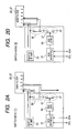
- Figs. 2A and 2B are diagrams illustrating an operation example of band switching of the digital SAW filter 25 and the analog SAW filter 27 for sound according to the embodiment.
- the control signal for turning on the transistor 57 is supplied to the bus interface 31 from the host.
- the band switching port 58 outputs the DC output corresponding to the control signal, which is instructed from the host, as the band switching signal.
- DC output of 5V is output to the base of the transistor 57 as the band switching signal, so that the collector-emitter of the transistor 57 is conducted.
- the transistor 57 is turned on by the DC 5V applied to the base thereof, so that the output terminal T2 of the integrated circuit MOP IC is grounded and the transistor 56 connected between the output terminals T1 and T2 is turned off.
- the second terminals of the digital SAW filter 25 and the analog SAW filter 27 for sound are grounded.
- Fig. 3A illustrates the terminal configuration of the digital SAW filter 25 and the state in which the second terminal is grounded.
- Fig. 3B illustrates band characteristics set in the digital SAW filter 25 in the ground state illustrated in Fig. 3A .
- a pass band of 7.80MHz is set in the digital SAW filter 25.
- Fig. 4A illustrates the terminal configuration of the analog SAW filter 27 for sound and the state in which the second terminal is grounded.
- Fig. 4B illustrates band characteristics set in the analog SAW filter 27 for sound in the ground state illustrated in Fig. 4A .
- a narrow band which has a center frequency of 40.4MHz, is set in the analog SAW filter 27 for sound.
- the first and second terminals of the digital SAW filter 25 and the analog SAW filter 27 for sound are short-circuited.
- a control signal for turning off the transistor 57 is supplied to the bus interface 31 from the host.
- the control signal is received in the band switching port 58, and is output to the base of the transistor 57 as DC output of 0V that causes the collector-emitter of the transistor 57 to be non-conductive.
- the transistor 57 is turned off, so that the output terminal T2 of the integrated circuit MOP IC is switched to an open state from the ground state.
- the transistor 56 connected between the output terminals T1 and T2 is turned on by a bias voltage of the bias resistor 55.
- the first and second terminals of the digital SAW filter 25 and the analog SAW filter 27 for sound are short-circuited.
- Fig. 3C illustrates the terminal configuration of the digital SAW filter 25 and the state in which the first and second terminals are short-circuited.
- Fig. 3D illustrates band characteristics set in the digital SAW filter 25 in the short-circuit state illustrated in Fig. 3C .
- a pass band of 6.80MHz is set in the digital SAW filter 25. That is, as compared with the band width set in the ground state of the second terminal illustrated in Fig. 3A , the bandwidth is reduced by IMHz.
- Fig. 4C illustrates the terminal configuration of the analog SAW filter 27 for sound and the state in which the first and second terminals are short-circuited.
- Fig. 4D illustrates band characteristics set in the analog SAW filter 27 for sound in the short-circuit state illustrated in Fig. 4C .
- a narrow band which has a center frequency of 32.4MHz to 33.4MHz, is set in the analog SAW filter 27 for sound. That is, the center frequency is shifted to a low frequency from 40.4MHz, which is set in the ground state of the second terminal illustrated in Fig. 4A , by 12 to 13MHz.
- control signal is supplied to the bus interface 31 from the host, so that the terminal states of input sections of the digital SAW filter 25 and the analog SAW filter 27 for sound are switched, thereby realizing band switching.
- the output circuit of the intermediate frequency amplifier 23 serves as a DC bias circuit of the transistor 56, so that it is possible to remove the DC bias circuit (DC cut capacitor C1 and resistors R1 and R2 of Fig. 8 ) which is necessary for the related art.
- the existing circuit illustrated in Figs. 6 and 8 since the potential difference occurs in the output voltage (output voltage of the intermediate frequency amplifier 23) of the integrated circuit MOP IC and the fixed bias by the resistors R1 and R2, dedicated bias circuits are necessary for the digital SAW filter 25 and the analog SAW filter 27 for sound.
- the output voltage of the intermediate frequency amplifier 23 serves as the reference potential of the transistor 56, so that RF switches can be unified in a digital/analog manner and the number of the RF switches can be reduced.
- the RF switches are unified in the digital/analog manner, control systems, which supply band switching instruction to the digital SAW filter 25 and the analog SAW filter 27 for sound, can be simplified through unification thereof.
- the DC switch which generates the band switching signal, has a circuit configuration (transistor 57) with the function of "open” and "ground", the DC switch and the RF switch can be used in common.
- the number of parts can be significantly reduced, so that the transistor 56 and the bias resistor 55 can be embedded in the integrated circuit MOP IC, and all circuit elements for band switching of the digital SAW filter 25 and the analog SAW filter 27 for sound can be incorporated in the integrated circuit MOP IC.
- interconnection work of the integrated circuit MOP IC and the SAW filters can be completed by merely connecting the first and second terminals of the digital SAW filter 25 and the analog SAW filter 27 for sound to the output terminals T1 and T2 of the integrated circuit MOP IC.
- the number of work steps can be significantly reduced, and soldering places can be reduced, thereby achieving the improvement of reliability.
- the DC cut capacitors C11 and C12 are connected to the first and second terminals of the digital SAW filter 25, respectively.
- the DC cut capacitors C11 and C12 can be removed if the above configuration belongs to a DC range which does not cause any problems in the DC resistance of the digital SAW filter 25. Consequently, the first and second terminals of the digital SAW filter 25 and the analog SAW filter 27 for sound are directly connected to the output terminals T1 and T2 of the integrated circuit MOP IC, so that the interconnection work is extremely simplified.
- Fig. 5 is a circuit diagram illustrating the configuration of the rear-stage of the intermediate frequency amplifier in the television receiver according to a modification of the invention.
- the configuration of the pre-stage of the intermediate frequency amplifier in the television receiver is identical to that of the television receiver illustrated in Fig. 6 .
- the intermediate frequency amplifier including digital elements (transistors 51 and 52 and resistors 53 and 54) and analog elements (transistors 61 and 62 and resistors 63 and 64), which are provided in parallel to each other, is provided in the integrated circuit MOP IC.
- An output voltage of the analog intermediate frequency amplifier appears in an output terminal T11 of the integrated circuit MOP IC.
- the gain control amplifier 29 connected to an output stage of the digital SAW filter 25 is embedded in the integrated circuit MOP IC.
- a transistor 65 serving as an RF switch for band switching of an input section of the analog SAW filter 27 for sound is embedded in an analog demodulator 60.
- the transistor 65 has a collector connected to a DC power supply terminal T21 of the analog demodulator 60, and an emitter connected to a ground terminal T22 thereof.
- a switch 71 provided in the form of a diode is connected between the first and second terminals of the digital SAW filter 25.
- a bias voltage is applied to an anode of the switch 71 through the bias resistor 55 and the anode is connected to the ground through the collector-emitter of the transistor 57.
- a switch 72 provided in the form of a diode is connected between the first and second terminals of the analog SAW filter 27 for sound.
- a bias voltage is applied to an anode of the switch 72 through a bias resistor 73 provided in the analog demodulator 60, and the anode is connected to the ground through the collector-emitter of the transistor 65 provided in the analog demodulator 60.
- the switch circuit (transistor 57) having functions of "ground” and “open” is disposed in the integrated circuit MOP IC to which the output signal of the digital SAW filter 25 is input, the ground of the switch circuit (switch 71) of the input section of the digital SAW filter 25 and the ground of the integrated circuit MOP IC can be commonly used. In this way, an optimal arrangement is achieved, so that the original properties of the digital SAW filter 25 can be further realized.
- the switch circuit (transistor 57) of the input section of the digital SAW filter 25 is disposed in the integrated circuit MOP IC in which the gain control amplifier 29 is embedded, so that a ground part of the digital SAW filter 25 and a ground part of the gain control amplifier 29 can be used in common, and the original transmission characteristics of the digital SAW filter 25 can be realized without being affected by the analog SAW filters 27 and 28.
- the switch circuit (transistor 65) of the input section of the analog SAW filter 27 for sound is disposed in the analog demodulator 60, so that a ground part of the analog SAW filter 27 for sound and a ground part of the analog demodulator 60 can be used in common, and the original transmission characteristics of the analog SAW filter 27 for sound can be realized without being affected by the digital SAW filter 25.
- the invention is not limited to the above-described embodiment.
- the above description has been given based on the system of the television receiver.
- the invention can similarly be applied to a high frequency apparatus if the purpose is to switch connection states of first and second terminals in the high frequency apparatus.
- the invention can be applied to a television receiver that performs a band switching operation by switching terminal connection states of the input sections of SAW filters in an intermediate frequency circuit.
Landscapes
- Electronic Switches (AREA)
- Filters And Equalizers (AREA)
Abstract
Provided is a high frequency apparatus including a first high frequency circuit (23) receiving a power supply voltage and having a high frequency signal output terminal, a second high frequency circuit (25, 27) connected to the high frequency signal output terminal and having first and second switch terminals to perform switching to a first or a second operation mode according to a connection state of the first and second switch terminals, a switch circuit interposed between the first high frequency circuit (23) and the second high frequency circuit (25, 27) to switch the connection state of the first and second switch terminals, and a control circuit applying a control signal to the switch circuit. The switch circuit includes a first switching device (57) and a second switching device (56).
Description
- The present invention claims the benefit of Japanese Patent Application
JP 2009-037797 - The present invention relates to a high frequency apparatus capable of performing a band switching operation by switching a terminal connection state of a SAW filter input section.
- In a television receiver, in order to reduce disturbance by an adjacent frequency, a SAW (Surface Acoustic Wave) filter is connected to a rear-stage of an intermediate frequency signal amplification circuit that amplifies an intermediate frequency signal supplied from a tuner. In a television receiver capable of receiving both terrestrial digital broadcasting and analog broadcasting is provided with a digital SAW filter compatible with a digital broadcasting signal and an analog SAW filter compatible with an analog broadcasting signal.
- However, when designing a television receiver compatible with Japanese and European television broadcasting schemes, it is necessary to allow the television receiver to be compatible with television broadcasting schemes of each country. The television broadcasting schemes of each country include PAL/B schemes, PAL/G schemes, PAL/D schemes, PAL/K schemes, NTSC/M schemes, NTSC/N schemes, SECAM/L schemes and the like. In particular, according to a SECAM/L scheme employed in France, in relation to four channels treated as a VHF low band, frequencies of an image signal carrier and a sound signal carrier are inverted to each other as compared with those in other VHF low band channels, VHF high band channels and UHF channels.
- In this regard, as an analog SAW filter, a SAW filter for an image is provided separately from a SAW filter for sound. Further, the SAW filter for sound is configured to switch a band according to the SECAM/L scheme.
-
Fig. 6 is a diagram illustrating the configuration of the television receiver compatible with an analog scheme and a digital scheme. In the television receiver illustrated inFig. 6 , after television signals received in atuner 1 are amplified by ahigh frequency amplifier 2, reception signals of a UHF band pass through a band-pass filter (BPF) 3, and reception signals of a VHF band pass through twoBPFs BPFs 3 to 5 are gain-controlled bygain control amplifiers 6 to 8, and then are input tocorresponding mixers RF filters 11 to 13.Oscillation circuits 16 to 18 are connected to themixers band limit circuits mixers band limit circuit 21 performs band limitation of a narrow band compatible with a digital scheme and theband limit circuit 22 performs band limitation of a wide band compatible with a PAL scheme. The signals having passed through theband limit circuits intermediate frequency amplifier 23 to a predetermined signal level, and then are input to adigital SAW filter 25 andanalog SAW filters gain control amplifier 29 is connected to an output stage of thedigital SAW filter 25. - Herein, the
digital SAW filter 25 is configured to perform a switching operation in limited bands of VHF and UHF. A band switching instruction is supplied to thedigital SAW filter 25 from aswitch circuit 24. Similarly to this, theanalog SAW filter 27 for sound is configured to switch bands according to a SECAM/L scheme. A band switching instruction is supplied to theanalog SAW filter 27 for sound from aswitch circuit 26. In relation to theswitch circuit 24 provided with respect to thedigital SAW filter 25, a control signal supplied to abus interface 31 from a host is converted to an ON/OFF signal by aDC switch 32, and then is supplied to theswitch circuit 24. Further, in relation to theswitch circuit 26 provided with respect to theanalog SAW filter 27 for sound, a control signal supplied to abus interface 33, which is provided in ananalog demodulator 30, from the host is converted to an ON/OFF signal by aDC switch 34 provided in theanalog demodulator 30, and then is supplied to theswitch circuit 26. - A band switching operation in the
digital SAW filter 25 will be described with reference toFigs. 7A and 7B . If a second terminal of thedigital SAW filter 25 is grounded, a first band is set. If a first terminal and the second terminal of thedigital SAW filter 25 are short-circuited, a second band is set. Theswitch circuit 24 includes aswitch 24b that grounds only the second terminal and aswitch 24a that short-circuits the first and second terminals. As illustrated inFig. 7A , only theswitch 24b is switched on by an ON/OFF signal supplied to theswitches DC switch 32, so that the first band is set. As illustrated inFig. 7B , only theswitch 24a is switched on, so that the second band is set. Theswitch circuit 26 provided with respect to theanalog SAW filter 27 for sound has a configuration similar to that of theswitch circuit 24, and the first band and the second band can be set in theanalog SAW filter 27 for sound. -
Fig. 8 is a circuit diagram illustrating the circuit configuration of theswitch circuit 24. An output terminal of theintermediate frequency amplifier 23 is connected to a first terminal (first pin) of thedigital SAW filter 25, and adiode 41 serving as a switching device is connected between the first terminal and a second terminal (second pin). A fixed bias divided by bias resistors R1 and R2 is applied to a cathode of thediode 41, and a predetermined voltage is applied to an anode of thediode 41 through a switching resistor R3. Further, the anode of thediode 41 is connected to the ground through a collector-emitter of atransistor 42. A control signal (ON/OFF signal) is applied to a base of thetransistor 42 from theDC switch 32, so that a connection state of the first and second terminals is switched. Since the voltage difference occurs between the fixed bias (e.g., 1.6V) generated by the bias resistors R1 and R2 and an output voltage (e.g., 2.1V) of theintermediate frequency amplifier 23, the output terminal of theintermediate frequency amplifier 23 is connected to the cathode of theswitching diode 41 through a DC cut capacitor C1. If thetransistor 42 is turned on (conductive), since the second terminal is grounded through the collector-emitter of thetransistor 42 and thediode 41 is turned off (not conductive), only the first terminal is connected to the output terminal of theintermediate frequency amplifier 23 in a high frequency manner. Further, if thetransistor 42 is turned off (not conductive), since thediode 41 is turned on (conductive), the first and second terminals are short-circuited. - The
switch circuit 26 having a configuration similar to that of theswitch circuit 24 illustrated inFig. 8 is provided with respect to theanalog SAW filter 27 for sound. Theswitch circuit 26 receives the control signal from theDC switch 34 provided in theanalog demodulator 30 to switch the connection state of the first and second terminals of theanalog SAW filter 27 for sound (for example, refer to Japanese Unexamined Patent Application Publication No.2008-028978 - However, in the above-described high frequency apparatus including the two switch circuits, since a plurality of elements for realizing the functions of the
switch circuits Fig. 8 , it is difficult to reduce the circuit size. Further, since the switch circuit with respect to the digital SAW filter and the switch circuit with respect to the analog SAW filter for sound are controlled by separate control systems, the control systems are complicated. - An advantage of some aspects of the invention is to provide a high frequency apparatus in which the circuit size of a switch circuit can be reduced and a control system can be simplified through unification thereof.
- According to an aspect of the invention, there is provided a high frequency apparatus including: a first high frequency circuit receiving a power supply voltage and having a high frequency signal output terminal; a second high frequency circuit connected to the high frequency signal output terminal and having first and second switch terminals to perform switching to a first or a second operation mode according to a connection state of the first and second switch terminals; a switch circuit interposed between the first high frequency circuit and the second high frequency circuit to switch the connection state of the first and second switch terminals; and a control circuit applying a control signal to the switch circuit, wherein the switch circuit includes: a first switching device having a control signal input terminal receiving the control signal, a ground terminal connected to a ground, and an output terminal connected to a supply terminal of the power supply voltage through a resistor, and switching on/off between the output terminal and the ground terminal; and a second switching device having one end connected to the output terminal of the first switching device and switching on/off between both ends of the second switching device, wherein a constant voltage for switching on or off the first and second switching devices is output from the high frequency signal output terminal, and the other end of the second switching device is connected to the high frequency signal output terminal in a direct-current manner.
- With such a configuration, the constant voltage for switching on or off the first and second switching devices is output from the high frequency signal output terminal, and the other end of the second switching device is connected to the high frequency signal output terminal in the direct-current manner, so that an output circuit of the first high frequency circuit serves as a DC bias circuit of the second switching device. Thus, differently from the related art in which the potential difference occurs in the output voltage of an intermediate frequency amplifier and a fixed bias by resistors of a fixed bias circuit, dedicated DC bias circuits provided for each of the second high frequency circuits can be unified, so that the number of switches can be reduced.
- Further, according to an embodiment of the high frequency apparatus of the invention, the first switch terminal is connected to the other end of the second switching device, the second switch terminal is connected to the output terminal of the first switching device, the second switching device is switched off when the first switching device is switched on, and the second switching device is switched on when the first switching device is switched off.
- Further, according to an embodiment of the high frequency apparatus of the invention, an output stage of the first high frequency circuit includes two transistors serially connected to the supply terminal of the power supply voltage and a ground, and the high frequency signal output terminal is connected to a connection point of the two transistors.
- Further, according to an embodiment of the high frequency apparatus of the invention, the second high frequency circuit is a SAW filter circuit which is in a first operation mode set to a first band characteristics when the first and second switch terminals are opened and the second switch terminal is grounded, and is in a second operation mode set to a second band characteristics different from the first band characteristics when the first and second switch terminals are short-circuited and the second switch terminal is opened with respect to the ground.
- Further, according to an embodiment of the high frequency apparatus of the invention, the first high frequency circuit and the switch circuit are formed in a single integrated circuit. Consequently, since the first high frequency circuit and the switch circuit are formed in the single integrated circuit, the interconnection work can be completed by merely connecting the switch terminal of the second high frequency circuit to the output terminal of an integrated circuit. Further, as compared with the related art, the number of work steps can be significantly reduced, and soldering places can be reduced, thereby achieving the improvement of reliability.
-
-
Fig. 1 is a circuit diagram mainly illustrating the circuit configuration for band switching of a digital SAW filter and an analog SAW filter for sound according to one embodiment. -
Figs. 2A and 2B are diagrams illustrating an operation example of band switching of a digital SAW filter and an analog SAW filter for sound according to one embodiment. -
Fig. 3A is a diagram illustrating a terminal configuration and a ground state of a digital SAW filter. -
Fig. 3B is a graph illustrating the band characteristics of a digital SAW filter in a ground state illustrated inFig. 3A . -
Fig. 3C is a diagram illustrating a terminal configuration and another ground state of a digital SAW filter. -
Fig. 3D is a graph illustrating the band characteristics of a digital SAW filter in a ground state illustrated inFig. 3C . -
Fig. 4A is a diagram illustrating a terminal configuration and a ground state of an analog SAW filter for sound. -
Fig. 4B is a graph illustrating the band characteristics of an analog SAW filter for sound in a ground state illustrated inFig. 4A . -
Fig. 4C is a diagram illustrating a terminal configuration and another ground state of an analog SAW filter for sound. -
Fig. 4D is a graph illustrating the band characteristics of an analog SAW filter for sound in a ground state illustrated inFig. 4C . -
Fig. 5 is a circuit diagram illustrating the configuration of the rear-stage of an intermediate frequency amplifier in a television receiver according to a modification of the invention. -
Fig. 6 is a diagram illustrating the configuration of a television receiver compatible with an analog scheme and a digital scheme. -
Figs. 7A and 7B are graphs illustrating an operation example of band switching of a digital SAW filter according to the related art. -
Fig. 8 is a circuit diagram illustrating the circuit configuration of a switch circuit of a SAW filter input section according to the related art. - An embodiment of the invention will be described in detail with reference to the accompanying drawings.
- A television receiver according to the embodiment of the invention is achieved by modifying the circuit configuration for band switching of a digital SAW filter and an analog SAW filter for sound.
-
Fig. 1 is a circuit diagram mainly illustrating the circuit configuration for band switching of a digital SAW filter and an analog SAW filter for sound. Further, the television receiver according to the embodiment includes elements identical to those of the television receiver illustrated inFig. 6 , except for the circuit configuration for performing the band switching, and the same reference numerals are used to designate the same elements as those ofFig. 6 in order to avoid the redundancy. - The
intermediate frequency amplifier 23 includestransistors transistor 51. An IF signal having an inverted phase is input to a base of thetransistor 52, so that drive capacity of thetransistor 51 is corrected. Theintermediate frequency amplifier 23 is a balance type amplifier and has the general circuit configuration illustrated inFig. 6 . That is, theintermediate frequency amplifier 23 includes two pairs of output circuits of thetransistors transistors 61 and 62 (not shown). Further, in order to correct the drive capacity, IF signals having an inverted phase are input to the bases of thetransistors transistor 51 located at a power supply side is connected to a power supply terminal T3, which serves as a supply terminal of a power supply voltage of an integrated circuit MOP IC, through abias resistor 53. Further, an emitter of thetransistor 52 located at a ground side is connected to the ground. Output of theintermediate frequency amplifier 23 is taken out from a connection point of an emitter of thetransistor 51 and a collector of thetransistor 52, and an output terminal T1 serving as a high frequency signal output terminal of the integrated circuit MOP IC is connected to the connection point through abias resistor 54. The output terminal T1 of the integrated circuit MOP IC is connected to first terminals (first pins) of thedigital SAW filter 25, theanalog SAW filter 27 for sound and theanalog SAW filter 28 for an image. Further, an output terminal T2 of the integrated circuit MOP IC is connected to second terminals (second pins) of thedigital SAW filter 25 and theanalog SAW filter 27 for sound. The power supply terminal T3 and the output terminal T2 of the integrated circuit MOP IC are connected to each other in a direct current manner through abias resistor 55. In addition, the output terminals T1 and T2 of the integrated circuit MOP IC are connected to each other through atransistor 56 serving as a switching device. A base of thetransistor 56 is connected to the output terminal T2, and the base and the collector of thetransistor 56 are connected to each other. Further, an emitter of thetransistor 56 is connected to the output terminal T1 in a direct current manner. In this way, the first and second terminals of thedigital SAW filter 25 and theanalog SAW filter 27 for sound are connected to each other through thetransistor 56. Further, the output terminal T2 (base of the transistor 56) is connected to the ground through a collector-emitter of atransistor 57 serving as a switching device. A band switching signal of ON/OFF is input to a base of thetransistor 57 serving as a control signal input terminal from aband switching port 58. Theband switching port 58 is a port in which DC output (e.g., 5V or 0V) appears in response to a control signal supplied to abus interface 31. The DC output of theband switching port 58 serves as the band switching signal. Similarly to the television receiver illustrated inFig. 6 , the band switching signal is controlled by the control signal supplied to thebus interface 31 from the host. Thetransistor 57 is turned on (conductive), so that the output terminal T2 (second terminals of thedigital SAW filter 25 and theanalog SAW filter 27 for sound) is grounded. Further, thetransistor 56 is turned off (not conductive), so that a non-conductive state is established between the output terminals T1 and T2. -
Figs. 2A and 2B are diagrams illustrating an operation example of band switching of thedigital SAW filter 25 and theanalog SAW filter 27 for sound according to the embodiment. - In the operation example of
Fig. 2A , only the second terminals of thedigital SAW filter 25 and theanalog SAW filter 27 for sound are grounded. The control signal for turning on thetransistor 57 is supplied to thebus interface 31 from the host. Theband switching port 58 outputs the DC output corresponding to the control signal, which is instructed from the host, as the band switching signal. Herein, DC output of 5V is output to the base of thetransistor 57 as the band switching signal, so that the collector-emitter of thetransistor 57 is conducted. Thetransistor 57 is turned on by the DC 5V applied to the base thereof, so that the output terminal T2 of the integrated circuit MOP IC is grounded and thetransistor 56 connected between the output terminals T1 and T2 is turned off. As a result, as illustrated inFig. 2A , only the second terminals of thedigital SAW filter 25 and theanalog SAW filter 27 for sound are grounded. -
Fig. 3A illustrates the terminal configuration of thedigital SAW filter 25 and the state in which the second terminal is grounded.Fig. 3B illustrates band characteristics set in thedigital SAW filter 25 in the ground state illustrated inFig. 3A . In the example, a pass band of 7.80MHz is set in thedigital SAW filter 25. -
Fig. 4A illustrates the terminal configuration of theanalog SAW filter 27 for sound and the state in which the second terminal is grounded.Fig. 4B illustrates band characteristics set in theanalog SAW filter 27 for sound in the ground state illustrated inFig. 4A . In the example, a narrow band, which has a center frequency of 40.4MHz, is set in theanalog SAW filter 27 for sound. - In the operation example of
Fig. 2B , the first and second terminals of thedigital SAW filter 25 and theanalog SAW filter 27 for sound are short-circuited. A control signal for turning off thetransistor 57 is supplied to thebus interface 31 from the host. The control signal is received in theband switching port 58, and is output to the base of thetransistor 57 as DC output of 0V that causes the collector-emitter of thetransistor 57 to be non-conductive. Thetransistor 57 is turned off, so that the output terminal T2 of the integrated circuit MOP IC is switched to an open state from the ground state. Thus, thetransistor 56 connected between the output terminals T1 and T2 is turned on by a bias voltage of thebias resistor 55. As a result, as illustrated inFig. 2B , the first and second terminals of thedigital SAW filter 25 and theanalog SAW filter 27 for sound are short-circuited. -
Fig. 3C illustrates the terminal configuration of thedigital SAW filter 25 and the state in which the first and second terminals are short-circuited.Fig. 3D illustrates band characteristics set in thedigital SAW filter 25 in the short-circuit state illustrated inFig. 3C . In the example, a pass band of 6.80MHz is set in thedigital SAW filter 25. That is, as compared with the band width set in the ground state of the second terminal illustrated inFig. 3A , the bandwidth is reduced by IMHz. -
Fig. 4C illustrates the terminal configuration of theanalog SAW filter 27 for sound and the state in which the first and second terminals are short-circuited.Fig. 4D illustrates band characteristics set in theanalog SAW filter 27 for sound in the short-circuit state illustrated inFig. 4C . In the example, a narrow band, which has a center frequency of 32.4MHz to 33.4MHz, is set in theanalog SAW filter 27 for sound. That is, the center frequency is shifted to a low frequency from 40.4MHz, which is set in the ground state of the second terminal illustrated inFig. 4A , by 12 to 13MHz. - In this way, the control signal is supplied to the
bus interface 31 from the host, so that the terminal states of input sections of thedigital SAW filter 25 and theanalog SAW filter 27 for sound are switched, thereby realizing band switching. - According to the embodiment as described above, since the output voltage of the
intermediate frequency amplifier 23, which appears in the output terminal T1 of the integrated circuit MOP IC, becomes a reference potential of thetransistor 56, the output circuit of theintermediate frequency amplifier 23 serves as a DC bias circuit of thetransistor 56, so that it is possible to remove the DC bias circuit (DC cut capacitor C1 and resistors R1 and R2 ofFig. 8 ) which is necessary for the related art. According to the existing circuit illustrated inFigs. 6 and8 , since the potential difference occurs in the output voltage (output voltage of the intermediate frequency amplifier 23) of the integrated circuit MOP IC and the fixed bias by the resistors R1 and R2, dedicated bias circuits are necessary for thedigital SAW filter 25 and theanalog SAW filter 27 for sound. However, according to the embodiment, the output voltage of theintermediate frequency amplifier 23 serves as the reference potential of thetransistor 56, so that RF switches can be unified in a digital/analog manner and the number of the RF switches can be reduced. - Further, according to the embodiment, the RF switches are unified in the digital/analog manner, control systems, which supply band switching instruction to the
digital SAW filter 25 and theanalog SAW filter 27 for sound, can be simplified through unification thereof. - Further, according to the embodiment, the DC switch, which generates the band switching signal, has a circuit configuration (transistor 57) with the function of "open" and "ground", the DC switch and the RF switch can be used in common.
- Furthermore, according to the embodiment, the number of parts can be significantly reduced, so that the
transistor 56 and thebias resistor 55 can be embedded in the integrated circuit MOP IC, and all circuit elements for band switching of thedigital SAW filter 25 and theanalog SAW filter 27 for sound can be incorporated in the integrated circuit MOP IC. In addition, interconnection work of the integrated circuit MOP IC and the SAW filters can be completed by merely connecting the first and second terminals of thedigital SAW filter 25 and theanalog SAW filter 27 for sound to the output terminals T1 and T2 of the integrated circuit MOP IC. Further, as compared with the related art, the number of work steps can be significantly reduced, and soldering places can be reduced, thereby achieving the improvement of reliability. - Moreover, the DC cut capacitors C11 and C12 are connected to the first and second terminals of the
digital SAW filter 25, respectively. However, the DC cut capacitors C11 and C12 can be removed if the above configuration belongs to a DC range which does not cause any problems in the DC resistance of thedigital SAW filter 25. Consequently, the first and second terminals of thedigital SAW filter 25 and theanalog SAW filter 27 for sound are directly connected to the output terminals T1 and T2 of the integrated circuit MOP IC, so that the interconnection work is extremely simplified. -
Fig. 5 is a circuit diagram illustrating the configuration of the rear-stage of the intermediate frequency amplifier in the television receiver according to a modification of the invention. The configuration of the pre-stage of the intermediate frequency amplifier in the television receiver is identical to that of the television receiver illustrated inFig. 6 . - The intermediate frequency amplifier including digital elements (
transistors resistors 53 and 54) and analog elements (transistors resistors 63 and 64), which are provided in parallel to each other, is provided in the integrated circuit MOP IC. An output voltage of the analog intermediate frequency amplifier appears in an output terminal T11 of the integrated circuit MOP IC. Further, thegain control amplifier 29 connected to an output stage of thedigital SAW filter 25 is embedded in the integrated circuit MOP IC. - In addition, a
transistor 65 serving as an RF switch for band switching of an input section of theanalog SAW filter 27 for sound is embedded in ananalog demodulator 60. Thetransistor 65 has a collector connected to a DC power supply terminal T21 of theanalog demodulator 60, and an emitter connected to a ground terminal T22 thereof. - A
switch 71 provided in the form of a diode is connected between the first and second terminals of thedigital SAW filter 25. A bias voltage is applied to an anode of theswitch 71 through thebias resistor 55 and the anode is connected to the ground through the collector-emitter of thetransistor 57. - Further, a
switch 72 provided in the form of a diode is connected between the first and second terminals of theanalog SAW filter 27 for sound. A bias voltage is applied to an anode of theswitch 72 through abias resistor 73 provided in theanalog demodulator 60, and the anode is connected to the ground through the collector-emitter of thetransistor 65 provided in theanalog demodulator 60. - According to the modification having the above-described configuration, the switch circuit (transistor 57) having functions of "ground" and "open" is disposed in the integrated circuit MOP IC to which the output signal of the
digital SAW filter 25 is input, the ground of the switch circuit (switch 71) of the input section of thedigital SAW filter 25 and the ground of the integrated circuit MOP IC can be commonly used. In this way, an optimal arrangement is achieved, so that the original properties of thedigital SAW filter 25 can be further realized. - In addition, the switch circuit (transistor 57) of the input section of the
digital SAW filter 25 is disposed in the integrated circuit MOP IC in which thegain control amplifier 29 is embedded, so that a ground part of thedigital SAW filter 25 and a ground part of thegain control amplifier 29 can be used in common, and the original transmission characteristics of thedigital SAW filter 25 can be realized without being affected by the analog SAW filters 27 and 28. - Moreover, the switch circuit (transistor 65) of the input section of the
analog SAW filter 27 for sound is disposed in theanalog demodulator 60, so that a ground part of theanalog SAW filter 27 for sound and a ground part of theanalog demodulator 60 can be used in common, and the original transmission characteristics of theanalog SAW filter 27 for sound can be realized without being affected by thedigital SAW filter 25. - The invention is not limited to the above-described embodiment. The above description has been given based on the system of the television receiver. However, the invention can similarly be applied to a high frequency apparatus if the purpose is to switch connection states of first and second terminals in the high frequency apparatus.
- The invention can be applied to a television receiver that performs a band switching operation by switching terminal connection states of the input sections of SAW filters in an intermediate frequency circuit.
- It should be understood by those skilled in the art that various modifications, combinations, sub-combinations and alterations may occur depending on design requirements and other factors insofar as they are within the scope of the appended claims of the equivalents thereof.
Claims (5)
- A high frequency apparatus comprising:a first high frequency circuit (23) receiving a power supply voltage and having a high frequency signal output terminal;a second high frequency circuit (25, 27) connected to the high frequency signal output terminal and having first and second switch terminals to perform switching to a first or a second operation mode according to a connection state of the first and second switch terminals;a switch circuit interposed between the first high frequency circuit (23) and the second high frequency circuit (25, 27) to switch the connection state of the first and second switch terminals; anda control circuit applying a control signal to the switch circuit,wherein the switch circuit includes:a first switching device (57) having a control signal input terminal receiving the control signal, a ground terminal connected to a ground, and an output terminal connected to a supply terminal (T3) of the power supply voltage through a resistor (55), and switching on/off between the output terminal and the ground terminal; anda second switching device (56) having one end connected to the output terminal of the first switching device (57) and switching on/off between both ends of the second switching device (56),wherein a constant voltage for switching on or off the first and second switching devices (57, 56) is output from the high frequency signal output terminal, and the other end of the second switching device (56) is connected to the high frequency signal output terminal in a direct-current manner.
- The high frequency apparatus according to claim 1, wherein the first switch terminal is connected to the other end of the second switching device (56), the second switch terminal is connected to the output terminal of the first switching device (57), the second switching device (56) is switched off when the first switching device (57) is switched on, and the second switching device is switched on when the first switching device is switched off.
- The high frequency apparatus according to claim 1 or 2, wherein an output stage of the first high frequency circuit (23) includes two transistors (51, 52) serially connected to the supply terminal of the power supply voltage and a ground, and the high frequency signal output terminal is connected to a connection point of the two transistors.
- The high frequency apparatus according to any one of claims 1 to 3, wherein the second high frequency circuit (25, 27) is a SAW filter circuit which is in a first operation mode set to a first band characteristics when the first and second switch terminals are opened and the second switch terminal is grounded, and is in a second operation mode set to a second band characteristics different from the first band characteristics when the first and second switch terminals are short-circuited and the second switch terminal is opened with respect to the ground.
- The high frequency apparatus according to any one of claims 1 to 4, wherein the first high frequency circuit (23) and the switch circuit are formed in a single integrated circuit.
Applications Claiming Priority (1)
| Application Number | Priority Date | Filing Date | Title |
|---|---|---|---|
| JP2009037797A JP2010193351A (en) | 2009-02-20 | 2009-02-20 | High-frequency apparatus |
Publications (1)
| Publication Number | Publication Date |
|---|---|
| EP2221967A1 true EP2221967A1 (en) | 2010-08-25 |
Family
ID=42224401
Family Applications (1)
| Application Number | Title | Priority Date | Filing Date |
|---|---|---|---|
| EP10153948A Withdrawn EP2221967A1 (en) | 2009-02-20 | 2010-02-18 | High frequency apparatus |
Country Status (2)
| Country | Link |
|---|---|
| EP (1) | EP2221967A1 (en) |
| JP (1) | JP2010193351A (en) |
Citations (2)
| Publication number | Priority date | Publication date | Assignee | Title |
|---|---|---|---|---|
| WO1994016498A1 (en) * | 1992-12-31 | 1994-07-21 | Motorola, Inc. | A multi-bandwidth saw filter |
| JP2008028978A (en) | 2006-06-20 | 2008-02-07 | Alps Electric Co Ltd | Antenna unit |
Family Cites Families (2)
| Publication number | Priority date | Publication date | Assignee | Title |
|---|---|---|---|---|
| DE19728315A1 (en) * | 1997-07-03 | 1999-01-07 | Philips Patentverwaltung | TV signal receiver |
| JP3572210B2 (en) * | 1998-12-14 | 2004-09-29 | アルプス電気株式会社 | Automatic fine tuning control voltage generation circuit |
-
2009
- 2009-02-20 JP JP2009037797A patent/JP2010193351A/en not_active Withdrawn
-
2010
- 2010-02-18 EP EP10153948A patent/EP2221967A1/en not_active Withdrawn
Patent Citations (2)
| Publication number | Priority date | Publication date | Assignee | Title |
|---|---|---|---|---|
| WO1994016498A1 (en) * | 1992-12-31 | 1994-07-21 | Motorola, Inc. | A multi-bandwidth saw filter |
| JP2008028978A (en) | 2006-06-20 | 2008-02-07 | Alps Electric Co Ltd | Antenna unit |
Non-Patent Citations (2)
| Title |
|---|
| "TWO SWITCHABLE SAW FILTERS IN A SINGLE PACKAGE", COMPONENTS, SIEMENS AKTIENGESELLSCHAFT. MUNCHEN, DE, vol. 32, no. 4, 1 January 1997 (1997-01-01), pages 26/27, XP000740376, ISSN: 0945-1137 * |
| FILBIG A A: "SWITCHABLE SAW FILTERS FOR MULTISTANDARD TELEVISION SETS", COMPONENTS, SIEMENS AKTIENGESELLSCHAFT. MUNCHEN, DE, vol. 27, no. 6, 1 November 1992 (1992-11-01), pages 11 - 14, XP000328744, ISSN: 0945-1137 * |
Also Published As
| Publication number | Publication date |
|---|---|
| JP2010193351A (en) | 2010-09-02 |
Similar Documents
| Publication | Publication Date | Title |
|---|---|---|
| US7756500B1 (en) | Active inductor circuits for filtering in a cable tuner circuit | |
| JP3263395B2 (en) | Gain control amplifier | |
| JPH0634378U (en) | Filter circuit | |
| WO2010076320A1 (en) | Amplifier with on-chip filter | |
| JPS61257012A (en) | Switching circuit array for two frequency bands changeable tuner | |
| US6084486A (en) | Controllable filter and high frequency apparatus using the same | |
| US8797097B2 (en) | Filtering device with low-pass filtering function and band-pass filtering function | |
| CN102035504B (en) | Intermediate frequency filter variable band pass | |
| EP1124329A2 (en) | Television tuner input circuit | |
| US8155609B2 (en) | Switch-able band-tracking input filter for combination tuner | |
| JPH0537406A (en) | China Circuit | |
| JP2010193351A (en) | High-frequency apparatus | |
| JPH02181524A (en) | Band switching filter circuit | |
| JP2578854B2 (en) | Receiver circuit | |
| JPH09130285A (en) | Input circuit for television tuner | |
| EP1522186B1 (en) | Television receiver with isolated inputs | |
| EP2222078B1 (en) | Intermediate frequency circuit | |
| US4178551A (en) | Bandwidth switching circuits of radio receiver | |
| JP3592971B2 (en) | Television tuner | |
| JP3103017U (en) | Television tuner | |
| CN201994923U (en) | Filtering channel control circuit of digital television | |
| JP2012195636A (en) | High frequency circuit and television receiver | |
| KR100703075B1 (en) | Signal attenuation circuit | |
| JPS6055713A (en) | filter circuit | |
| JPH0685571A (en) | Broadband high frequency amplifier |
Legal Events
| Date | Code | Title | Description |
|---|---|---|---|
| PUAI | Public reference made under article 153(3) epc to a published international application that has entered the european phase |
Free format text: ORIGINAL CODE: 0009012 |
|
| AK | Designated contracting states |
Kind code of ref document: A1 Designated state(s): AT BE BG CH CY CZ DE DK EE ES FI FR GB GR HR HU IE IS IT LI LT LU LV MC MK MT NL NO PL PT RO SE SI SK SM TR |
|
| AX | Request for extension of the european patent |
Extension state: AL BA RS |
|
| 17P | Request for examination filed |
Effective date: 20110217 |
|
| STAA | Information on the status of an ep patent application or granted ep patent |
Free format text: STATUS: THE APPLICATION HAS BEEN WITHDRAWN |
|
| 18W | Application withdrawn |
Effective date: 20130325 |