EP2219104A2 - Position indicator, circuit component and input device - Google Patents
Position indicator, circuit component and input device Download PDFInfo
- Publication number
- EP2219104A2 EP2219104A2 EP10000639A EP10000639A EP2219104A2 EP 2219104 A2 EP2219104 A2 EP 2219104A2 EP 10000639 A EP10000639 A EP 10000639A EP 10000639 A EP10000639 A EP 10000639A EP 2219104 A2 EP2219104 A2 EP 2219104A2
- Authority
- EP
- European Patent Office
- Prior art keywords
- position indicator
- coil
- magnetic core
- circuit
- core member
- Prior art date
- Legal status (The legal status is an assumption and is not a legal conclusion. Google has not performed a legal analysis and makes no representation as to the accuracy of the status listed.)
- Granted
Links
Images


Classifications
-
- G—PHYSICS
- G06—COMPUTING; CALCULATING OR COUNTING
- G06F—ELECTRIC DIGITAL DATA PROCESSING
- G06F3/00—Input arrangements for transferring data to be processed into a form capable of being handled by the computer; Output arrangements for transferring data from processing unit to output unit, e.g. interface arrangements
- G06F3/01—Input arrangements or combined input and output arrangements for interaction between user and computer
- G06F3/03—Arrangements for converting the position or the displacement of a member into a coded form
- G06F3/033—Pointing devices displaced or positioned by the user, e.g. mice, trackballs, pens or joysticks; Accessories therefor
- G06F3/038—Control and interface arrangements therefor, e.g. drivers or device-embedded control circuitry
-
- G—PHYSICS
- G01—MEASURING; TESTING
- G01D—MEASURING NOT SPECIALLY ADAPTED FOR A SPECIFIC VARIABLE; ARRANGEMENTS FOR MEASURING TWO OR MORE VARIABLES NOT COVERED IN A SINGLE OTHER SUBCLASS; TARIFF METERING APPARATUS; MEASURING OR TESTING NOT OTHERWISE PROVIDED FOR
- G01D5/00—Mechanical means for transferring the output of a sensing member; Means for converting the output of a sensing member to another variable where the form or nature of the sensing member does not constrain the means for converting; Transducers not specially adapted for a specific variable
- G01D5/12—Mechanical means for transferring the output of a sensing member; Means for converting the output of a sensing member to another variable where the form or nature of the sensing member does not constrain the means for converting; Transducers not specially adapted for a specific variable using electric or magnetic means
- G01D5/14—Mechanical means for transferring the output of a sensing member; Means for converting the output of a sensing member to another variable where the form or nature of the sensing member does not constrain the means for converting; Transducers not specially adapted for a specific variable using electric or magnetic means influencing the magnitude of a current or voltage
- G01D5/24—Mechanical means for transferring the output of a sensing member; Means for converting the output of a sensing member to another variable where the form or nature of the sensing member does not constrain the means for converting; Transducers not specially adapted for a specific variable using electric or magnetic means influencing the magnitude of a current or voltage by varying capacitance
- G01D5/241—Mechanical means for transferring the output of a sensing member; Means for converting the output of a sensing member to another variable where the form or nature of the sensing member does not constrain the means for converting; Transducers not specially adapted for a specific variable using electric or magnetic means influencing the magnitude of a current or voltage by varying capacitance by relative movement of capacitor electrodes
-
- G—PHYSICS
- G06—COMPUTING; CALCULATING OR COUNTING
- G06F—ELECTRIC DIGITAL DATA PROCESSING
- G06F3/00—Input arrangements for transferring data to be processed into a form capable of being handled by the computer; Output arrangements for transferring data from processing unit to output unit, e.g. interface arrangements
- G06F3/01—Input arrangements or combined input and output arrangements for interaction between user and computer
- G06F3/03—Arrangements for converting the position or the displacement of a member into a coded form
- G06F3/033—Pointing devices displaced or positioned by the user, e.g. mice, trackballs, pens or joysticks; Accessories therefor
- G06F3/0354—Pointing devices displaced or positioned by the user, e.g. mice, trackballs, pens or joysticks; Accessories therefor with detection of 2D relative movements between the device, or an operating part thereof, and a plane or surface, e.g. 2D mice, trackballs, pens or pucks
- G06F3/03545—Pens or stylus
-
- G—PHYSICS
- G06—COMPUTING; CALCULATING OR COUNTING
- G06F—ELECTRIC DIGITAL DATA PROCESSING
- G06F3/00—Input arrangements for transferring data to be processed into a form capable of being handled by the computer; Output arrangements for transferring data from processing unit to output unit, e.g. interface arrangements
- G06F3/01—Input arrangements or combined input and output arrangements for interaction between user and computer
- G06F3/03—Arrangements for converting the position or the displacement of a member into a coded form
- G06F3/041—Digitisers, e.g. for touch screens or touch pads, characterised by the transducing means
- G06F3/047—Digitisers, e.g. for touch screens or touch pads, characterised by the transducing means using sets of wires, e.g. crossed wires
Definitions
- the present invention relates to a position indicator whose rotation angle with respect to an axial direction can be detected, a circuit component used in the position indicator, and an input device having the position indicator.
- Such input devices generally comprise a pen-like position indicator and a position detecting device having an input surface, on which an input operation is performed using the position indicator.
- An input operation using the position indicator may include, for example, a pointing operation, a handwritten character input operation, or a hand-drawn illustration input operation.
- Patent Document 1 An example of such a kind of the input device is disclosed in Japanese Unexamined Patent Application Publication No. H08-30374 (referred to as "Patent Document 1" hereinafter).
- the input device disclosed in Patent Document 1 includes a position indicator having two cylindrical magnetic cores. The two magnetic cores are disposed so that a midpoint thereof is matched with a bar-like rod (providing a pen-tip at its distal end) of the position indicator.
- a control coil is wound around one of the two magnetic cores. Further, a transmission coil is wound around the two magnetic cores so that the two magnetic cores are bundled together. The transmission coil and a capacitor constitute a resonant circuit. Further, by controlling the opening/closing of the control coil, distribution of the magnetic flux passing through the transmission coil is changed, to thereby detect rotation angle and tilt angle of the position indicator.
- Patent Document 2 Another example of the input device capable of detection rotation/tilt of the position indicator is disclosed in Japanese Unexamined Patent Application Publication No. H08-202489 (referred to as "Patent Document 2" hereinafter).
- the input device disclosed in Patent Document 2 includes a position indicator having two parallelepiped-shaped magnetic cores. The two magnetic cores are disposed so that they sandwich a pen-tip of the position indicator. When the two magnetic cores are combined, the axis in the longitudinal direction of the two magnetic cores is matched with the pen-tip.
- Each of the magnetic cores has a control coil transversely wound therearound. Further, a transmission coil is transversely wound around the two magnetic cores so that the two magnetic cores are bundled together.
- the axis of the transmission coil, the position of the pen-tip, the axis of the position indicator, and the axis in the longitudinal direction of the two magnetic cores bundled together are all aligned with each other.
- the input device includes a tablet, which has a detection circuit for detecting a tilt-detecting signal generated from the control coil(s), and a control circuit for determining the tilt angle of the position indicator based on the result detected by the detection circuit.
- the position indicator disclosed in Patent Document 1 since the two cylindrical magnetic cores are disposed side by side in a direction perpendicular to the axis of the position indicator, the position indicator has a relatively large outer diameter.
- the two magnetic cores need to be sufficiently spaced apart from each other to prevent the rod, which passes therebetween, from interfering with the coil wound around each magnetic core. Thus, it was difficult to reduce the outer diameter of the position indicator. Still further, when the rod is not passed between the two magnetic cores, in order to connect the rod to a pen pressure detection switch provided at an end portion of the magnetic cores, to additionally detect the pen pressure, the rod has to be formed in a special (e.g., bent) shape, or an adapter has to be arranged between the rod and the switch.
- a pen pressure detection switch provided at an end portion of the magnetic cores
- an object of the present invention is to make it possible to detect the rotation (roll) of the position indicator with respect to an axial direction, and to detect the pen pressure without having to form the rod in a special shape.
- a position indicator includes: a tubular core member; a first coil; a second coil; a substantially bar-like rod; a pen-pressure detecting element; a capacitor; and a switch.
- the tubular core member has a through-hole.
- the tubular member is formed by combining a substantially bar-like first magnetic core with a substantially bar-like second magnetic core in a manner in which they face each other in a transversal direction thereof so that the through-hole is formed therebetween.
- the first coil is wound around the tubular core member.
- the second coil is wound around the second magnetic core, which forms the tubular core member.
- the substantially bar-like rod is inserted into the through-hole of the tubular core member.
- the pen-pressure detecting element detects a pressure applied to an end of the rod.
- the capacitor is connected to the first coil and is provided for forming a resonant circuit.
- the switch controls on/off of the second coil.
- a circuit component includes: a tubular core member; a first coil; and a second coil.
- the tubular core member has a through-hole and is formed by combining a substantially bar-like first magnetic core with a substantially bar-like second magnetic core such that they face each other in a transversal direction thereof so that the through-hole is formed.
- the first coil is wound around the tubular core member.
- the second coil is wound around the second magnetic core.
- An input device includes: a position indicator and a position detecting device.
- the position indicator includes: a tubular core member; a first coil; a second coil; a substantially bar-like rod; a pen-pressure detecting element; a capacitor; and a switch.
- the tubular core member has a through-hole.
- the tubular core member is formed by combining a substantially bar-like first magnetic core with a substantially bar-like second magnetic core such that they face each other in a transversal direction thereof thereby forming the through-hole therebetween.
- the first coil is wound around the tubular core member.
- the second coil is wound around the second magnetic core.
- the substantially bar-like rod is inserted into the through-hole of the tubular core member.
- the pen-pressure detecting element detects a pressure applied to an end of the rod.
- the capacitor is connected to the first coil and is provided for forming a resonant circuit.
- the switch controls on/off of the second coil.
- the position detecting device includes: an input surface on which the position indicator indicates a position, a coordinate input circuit, and a rotation angle calculating circuit.
- the coordinate input circuit obtains coordinates of the position indicated on the input surface based on distribution of a magnetic field emitted from the tubular core member of the position indicator.
- the rotation angle calculating circuit calculates a rotation angle of the position indicator around (about) an axis in a direction perpendicular to the input surface based on coordinates obtained when the switch is in a closed state and in an open state.
- the present invention it is possible to detect the rotation (roll) of the position indicator with respect to the axial direction of the position indicator and to also detect the pen pressure with a bar-like rod.
- FIGS. 1 to 14B A position indicator and an input device according to a first embodiment of the present invention will be described below with reference to FIGS. 1 to 14B . Note that, in the drawings, like components are denoted by like numerals.
- the input device 10 includes a position detecting device 1 and a position indicator 2 that inputs information to the position detecting device 1.
- the position indicator 2 indicates its own position on the position detecting device 1 based on the electromagnetic resonance technology.
- the configuration of the position detecting device 1 will be described below.
- the position detecting device 1 includes a detection section 4 for detecting the position indicated by the position indicator 2, and a case 5 for housing the detection section 4.
- the case 5 is a substantially rectangular parallelepiped-shaped case with a thin wall.
- the case 5 includes an upper case 7 and a lower case (not shown) coupled with the upper case 7.
- the upper case 7 has an opening 6 through which an input surface 4a of the detection section 4 is exposed.
- the position detecting device 1 is electrically connected to an external device (not shown), such as a personal computer, a PDA (Personal Digital Assistant), and the like, through a cable 8.
- an external device such as a personal computer, a PDA (Personal Digital Assistant), and the like
- the position detecting device according to the present invention may also be integrated with the external device such as a personal computer and the like.
- the position indicated on the input surface 4a of the detection section 4 by the position indicator 2 performing a pointing operation is detected by the position detecting device 1.
- the position detecting device 1 transmits position information representing the position indicated by the pointing operation to the external device.
- a hand-drawn illustration input operation, a handwritten character input operation or the like can be performed using various software installed on the external device.
- the detection section 4 of the position detecting device 1 has a position detecting coil 11 configured by superimposing an X-axis direction loop coil group 11a and a Y-axis direction loop coil group 11b.
- Each of the loop coil groups 11a, 11b comprises, for example, forty rectangular loop coils.
- the loop coils of each of the loop coil group 11a and loop coil group 11b are sequentially overlapped with each other so that the loop coils are shifted from each other at an equal interval.
- the position detecting device 1 is provided with a selecting circuit 12 to which the X-axis direction loop coil group 11a and the Y-axis direction loop coil group 11b are connected.
- the selecting circuit 12 sequentially selects a loop coil from the loop coil group 11a and loop coil group 11b.
- the position detecting device 1 further includes an oscillator 13, a current driver 14, a switching circuit 15, a receiving amplifier 16, a detector 17, a low-pass filter 18, a S/H circuit 19, an A/D conversion circuit 20, a synchronous detector 21, a low-pass filter 22, a S/H circuit 23, an A/D conversion circuit 24, and a processing portion 25.
- the oscillator 13 generates an AC signal having a frequency f0, and supplies the AC signal to the current driver 14 and the synchronous detector 21.
- the current driver 14 converts the AC signal supplied from the oscillator 13 into a current and sends the current to the switching circuit 15.
- the switching circuit 15 switches the connection of the loop coil selected by the selecting circuit 12 between two terminals to be connected (i.e., a transmission side terminal T and a reception side terminal R) under the control of the processing portion 25, which is to be described later.
- the transmission side terminal T has the current driver 14 connected thereto
- the reception side terminal R has the receiving amplifier 16 connected thereto.
- the induced voltage generated by the loop coil selected by the selecting circuit 12 is supplied to the receiving amplifier 16 through the selecting circuit 12 and the switching circuit 15.
- the receiving amplifier 16 amplifies the induced voltage supplied from the loop coil, and sends the amplified induced voltage to the detector 17 and the synchronous detector 21.
- the detector 17 detects the induced voltage generated by the loop coil (i.e., the detector 27 detects a received signal) and sends the detected signal to the low-pass filter 18.
- the S/H circuit 19 holds a voltage value of the signal output from the low-pass filter 18 at a predetermined timing (more specifically, at a predetermined time during a reception period), and sends the held value to the A/D conversion circuit (analog to digital conversion circuit) 20.
- the A/D conversion circuit 20 analog/digital converts the value output from the S/H circuit 19, and outputs the result to the processing portion 25.
- the synchronous detector 21 synchronously detects the output signal from the receiving amplifier 16 with the AC signal from the oscillator 13, and sends a signal, whose level varies corresponding to the phase difference between the both signals, to the low-pass filter 22.
- the low-pass filter 22, which has a cut-off frequency sufficiently lower than the frequency f0, converts the signal output from the synchronous detector 21 into a DC signal, and sends the DC signal to the S/H circuit (sample-and-hold circuit) 23.
- the S/H circuit 23 holds a voltage value of the output signal from the low-pass filter 22 at a predetermined timing, and sends the held value to the A/D conversion circuit (analog to digital conversion circuit) 24.
- the A/D conversion circuit 24 analog/digital converts the value output from the S/H circuit 23, and outputs the result to the processing portion 25.
- the processing portion 25 controls the respective sections of the position detecting device 1. Specifically, the processing portion 25 respectively controls the selecting operation of the loop coil performed by the selecting circuit 12, the switching operation performed by the switching circuit 15, and the determination of the timing at which the S/H circuits 19 and 23 hold the voltage value. Based on the signals input from the A/D conversion circuits 20 and 24, the processing portion 25 makes the X-axis direction loop coil group 11a and the Y-axis direction loop coil group 11b transmit an electromagnetic wave for a predetermined period.
- the processing portion 25 calculates the coordinate values of the position indicated by the position indicator 2 in both the X-axis direction and the Y-axis direction, a rotation angle of the position indicator 2 around an axis in the direction perpendicular to the input surface 4a, and the like.
- the position indicator 2 has a resonant circuit (see FIG. 6 ), which resonates with the electromagnetic wave of a specific frequency transmitted from the position detecting device 1. By generating the induced voltage in the resonant circuit, the position indicator 2 transmits an electromagnetic wave of frequency f0 to the position detecting device 1 to indicate its own position with respect to the position detecting device 1.
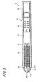
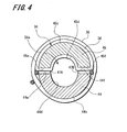
- the position indicator 2 includes a case 31 (as an example of an exterior component), a rod 32, a tubular core member 34, a first coil 35, a second coil 36 (see FIG. 4 ), a variable capacitor 37 (as an example of a pen-pressure detecting element), and a printed circuit board 38.
- the tubular core member 34, the first coil 35, and the second coil 36 form a circuit component of the present invention.
- the case 31 (as the exterior component of the position indicator 2) comprises, for example, a bottomed cylindrical case with one end thereof closed.
- the case 31 includes a first case 41 and a second case 42.
- the first case 41 and second case 42 are coupled with each other in the axial direction.
- One end in the axial direction of the first case 41 is substantially cone-shaped, and an opening 41a is formed on the tip of the cone-shaped end. Further, an opening is formed on the other end in the axial direction of the first case 41.
- the rod 32, the tubular core member 34, and the variable capacitor 37 are arranged inside the first case 41 in the illustrated example.
- the second case 42 is a cylindrical case having one end thereof opened and the other end thereof closed.
- the one end of the second case 42 is fixed to the other end of the first case 41 by a fixing means such as an adhesive or a fixing screw.
- the printed circuit board 38 having electronic components mounted thereon is fixed inside the second case 42 by a fixing means such as an adhesive or a fixing screw.
- the rod 32 is a substantially bar-like member.
- the rod 32 includes a pen-tip 32a formed at one end in the axial direction and a shaft portion 32b formed continuously from the pen-tip 32a.
- the pen-tip 32a is substantially cone-shaped. The pen-tip 32a protrudes to the outside of the first case 41 from the opening 41a.
- the shaft portion 32b penetrates through a through-hole 34a (see FIG. 4 ) of the tubular core member 34.
- a conductive member (not shown) of the variable capacitor 37 is provided at an end portion of the shaft portion 32b opposite the pen-tip 32a.
- the capacitance of the variable capacitor 37 changes according to the change of the pressure applied from the outside, and the pen pressure applied to the rod 32 is detected based on the change of the capacitance of the variable capacitor 37.
- tubular core member 34 the tubular core member 34, the first coil 35, and the second coil 36 will be described below with reference to FIGS. 4 and 5 .
- the tubular core member 34 includes a first magnetic core 44 and a second magnetic core 45.
- the tubular core member 34 has a hollow cylindrical shape with the through-hole 34a.
- the tubular core member 34 is formed by combining the two magnetic cores 44, 45 in a manner in which they face each other in a direction perpendicular to the axial direction of the case 31 so that the through-hole 34a is formed therebetween.
- the two magnetic cores 44, 45 are formed in substantially the same shape as each other in the illustrated embodiment.
- the two magnetic cores 44, 45 are each formed in an arc shape with a central angle of substantially 180°.
- the two magnetic cores 44, 45 are preferably made of, for example, a ferrite material.
- the first magnetic core 44 has two end surfaces 44a, 44b opposite each other, an arc-shaped convex surface 44c, an arc-shaped concave surface 44d, and two flat surfaces 44e, 44f each being perpendicular to the two end surfaces 44a, 44b.
- the second magnetic core 45 has two end surfaces 45a, 45b, an arc-shaped convex surface 45c, an arc-shaped concave surface 45d, and two flat surfaces 45e, 45f.
- the tubular core member 34 is formed by the two magnetic cores 44, 45, the two flat surfaces 44e, 44f of the first magnetic core 44 respectively face the two flat surfaces 45e, 45f of the second magnetic core 45. Further, the convex surface 44c of the first magnetic core 44 and the convex surface 45c of the second magnetic core 45 form the circumferential surface of the tubular core member 34. The concave surface 44d of the first magnetic core 44 and the concave surface 45d of the second magnetic core 45 form the through-hole 34a of the tubular core member 34.
- the first coil 35 is wound around the circumferential surface of the tubular core member 34.
- the second coil 36 is wound around the circumferential surface of the second magnetic core 45.
- the second coil 36 is wound so that the second coil 36 is curved along the concave surface 45d of the second magnetic core 45. Due to such an arrangement, even if the diameter of the rod 32 and the diameter of the through-hole 34a of the tubular core member 34 are substantially equal to each other, the rod 32 does not interfere with the second coil 36.
- the ends of the first coil 35 and the ends of the second coil 36 are arranged at one end portion of the tubular core member 34 in the longitudinal direction so as to be respectively connected to a capacitor 52 and a switch 55 (see FIG. 6 ).
- the tubular core member 34 is assembled in the following steps. First, the second coil 36 is wound around the circumferential surface of the second magnetic core 45. Then, the first magnetic core 44 and the second magnetic core 45 are disposed so that the flat surfaces 44e, 44f of the first magnetic core 44 and the flat surfaces 45e, 45f of the second magnetic core 45 respectively face each other. At this time, a spacer 47A is interposed between the flat surface 44e and the flat surface 45e, and a spacer 47B is interposed between the flat surface 44f and the flat surface 45f.
- the spacers 47A, 47B are provided to prevent or reduce the effect of the current flowing in the second coil 36 on the first magnetic core 44.
- the spacers 47A, 47B are made of a nonmagnetic insulating material.
- a synthetic resin such as polyethylene terephthalate (PET) can be used as the material of the spacers 47A, 47B.
- PET polyethylene terephthalate
- the thickness of the spacers 47A, 47B is preferably within a range of 100-500 ⁇ m.
- the first coil 35 is wound around the first magnetic core 44 and the second magnetic core 45 so that the convex surface 44c of the first magnetic core 44 and the convex surface 45c of the second magnetic core 45 are continuous with each other.
- the first coil 35 is wound around the circumferential surface of the tubular core member 34.
- the position indicator 2 is provided with a resonant circuit 51.
- the resonant circuit 51 includes the first coil 35, a capacitor 52 connected in parallel with the first coil 35, and the variable capacitor 37 connected in parallel with the capacitor 52.
- a capacitor 53 is connected to the resonant circuit 51 through a switch 54.
- a switch 55 is connected to the second coil 36 of position indicator 2.
- the capacitor 53 is provided for compensating for the drop of the inductance of the first coil 35 when closing the switch 55.
- the capacitance of the capacitor 53 is determined so that the resonance frequency of the resonant circuit 51 becomes a predetermined value (i.e., the frequency of the transmitting signal) independently of the control of the switch 55.
- a power supply circuit 61, a detection circuit 62, and a detection circuit 63 are respectively connected to the resonant circuit 51.
- An integrating circuit 64 is connected to the detection circuit 62, and an integrating circuit 65 is connected to the detection circuit 63. Further, a comparator 66 is connected to the integrating circuit 64, and a comparator 67 is connected to the integrating circuit 65.
- the output of the comparator 66 is connected to a data terminal of a latch circuit 68, and the output of the comparator 67 is connected to a trigger terminal of the latch circuit 68. Further, the switches 54, 55 are connected to the latch circuit 68.
- the power supply circuit 61 extracts the power from the induced voltage generated by the resonant circuit 51.
- the power stored in the power supply circuit 61 is supplied to the respective circuits of the position indicator 2.
- the detection circuit 62, the integrating circuit 64, and the comparator 66 form a first path 57 for providing output to the data terminal of the latch circuit 68.
- the detection circuit 62 generates clocks corresponding to the cycle lengths of transmission and intermission of the transmission electromagnetic wave transmitted by the position detecting device 1.
- the time constant of the integrating circuit 64 is greater than that of the integrating circuit 65.
- the comparator 66 compares the output signal of the integrating circuit 64 with a predetermined threshold voltage (for example, 50% of the power voltage), and converts the output signal into a digital signal.
- a predetermined threshold voltage for example, 50% of the power voltage
- the time constant of the integrating circuit 64 is set such that the output of the comparator 66 rises if the transmission time of the transmission electromagnetic wave transmitted by the position detecting device 1 exceeds a first predetermined time (500 ⁇ s, for example).
- the detection circuit 63, the integrating circuit 65, and the comparator 67 form a second path 58 for providing output to the trigger terminal of the latch circuit 68. Similar to the detection circuit 62, the detection circuit 63 generates clocks corresponding to the cycle lengths of transmission and intermission of the transmission electromagnetic wave transmitted by the position detecting device 1.
- the comparator 67 compares the output signal of the integrating circuit 65 with a predetermined threshold voltage (for example, 50% of the power voltage), and converts the output signal into a digital signal.
- a predetermined threshold voltage for example, 50% of the power voltage
- the time constant of the integrating circuit 65 is set such that the output of the comparator 67 rises if the transmission time of the transmission electromagnetic wave transmitted by the position detecting device 1 exceeds a second predetermined time (150 ⁇ s, for example), which is shorter than the first predetermined time.
- FIG. 7 is a flowchart showing processes executed by the processing portion 25 of the position detecting device 1.
- FIG. 8 is a waveform diagram showing the waveforms of the respective sections while sequentially scanning the respective loop coils of the X-axis direction loop coil group 11a.
- the processing portion 25 sequentially scans/selects the respective loop coils of the X-axis direction loop coil group 11a (Step S1) in order to detect whether or not the position indicator 2 is located near the detection section 4 of the position detecting device 1.
- the operation of sequentially scanning/selecting the loop coils is referred to as "global scanning” hereinafter.
- the global scanning (X-axis global scanning) will be described below with reference to FIG. 8 .
- the switches 54, 55 are in open state.
- the processing portion 25 sends information to the selecting circuit 12 to make it select a first loop coil (loop coil X 1 , for example) from the X-axis direction loop coil group 11a, and sends a signal to the switching circuit 15 to make it select the transmission side terminal T.
- a sinusoidal signal having the frequency f0 is supplied from the oscillator 13 to the loop coil X 1 , and a transmission electromagnetic wave (a) having the frequency f0 is generated by the loop coil X 1 .
- the processing portion 25 After the processing portion 25 sends the signal to the switching circuit 15 to make it select the transmission side terminal T for a predetermined period, a signal whose amplitude gradually increases with the lapse of time is generated in the resonant circuit 51 of the position indicator 2. Next, the processing portion 25 sends a signal to the switching circuit 15 to make it select the reception side terminal R. Accordingly transmission of the signal from the loop coil X 1 is stopped. However, the signal in the resonant circuit 51 attenuates gradually with the lapse of time, instead of disappearing immediately. In the meantime, a signal whose level varies corresponding to the signal in the resonant circuit 51 is induced in the loop coil X 1 . The signal generated in the loop coil X 1 is supplied to the receiving amplifier 16 through the switching circuit 15.
- the processing portion 25 After the processing portion 25 sends the signal to the switching circuit 15 to make it select the reception side terminal R for a predetermined period, the processing portion 25 makes the selecting circuit 12 select a second loop coil (loop coil X 2 , for example) from the X-axis direction loop coil group 11a. Further, the processing portion 25 sends information to make the switching circuit 15 select the transmission side terminal T. Next, the processing portion 25 sends a signal to the switching circuit 15 to make it select the reception side terminal R and thereby receive a signal induced in the loop coil X 2 in the same manner as described above.
- a second loop coil loop coil X 2 , for example
- the processing portion 25 performs the similar processing to sequentially scan/select 3rd to 40th loop coils (loop coils X 3 to X 40 , for example) of the X-axis direction loop coil group 11a.
- transmission/reception of the electromagnetic wave is performed on each of loop coils X 3 to X 40 .
- the resonant circuit 51 having the first coil 35 will be excited by the transmission electromagnetic wave (a) generated by the loop coil X 1 closest to the position indicator 2.
- an induced voltage (b) having the frequency f0 is generated in the resonant circuit 51.
- the present embodiment is based on an example in which every loop coil is scanned/selected.
- the processing portion 25 does not have to select every loop coil of the X-axis direction loop coil group 11a, but can select every other loop coil, every third loop coils, or the like.
- transmission/reception of the electromagnetic wave may also be performed plural times on the selected loop coil.
- the transmission time for each loop coil is equal and that the reception time for each loop coil is equal, the transmission time and the reception time do not have to be equal to each other.
- the induced voltage, i.e., a received signal (m), generated in the loop coil of the X-axis direction loop coil group 11a during the reception period is detected by the detector 17, converted into the DC signal, and smoothed by the low-pass filter 18. Further, the signal output by the low-pass filter 18 is held by the S/H circuit 19 at a predetermined timing to become a hold output (n), the hold output (n) is converted into a digital value by the A/D conversion circuit 20, and the digital value is sent to the processing portion 25.
- the output level of the S/H circuit 19 depends on the distance between the position indicator 2 and the loop coil.
- the processing portion 25 determines whether or not the maximum value of the digital value output by the A/D conversion circuit 20 is equal to or larger than a preset value (Step S2), and thereby determines whether or not the position indicator 2 is located within an effective reading height range of the position detecting device 1.
- Step S2 if it is determined that the maximum value of the digital value output by the A/D conversion circuit 20 is smaller than the preset value, i.e., if it is determined that the position indicator 2 is not located within the effective reading height range (i.e., "NO" in Step S2), the processing portion 25 returns the processing to Step S1.
- the processing portion 25 extracts, among the loop coils X 1 to X 40 , a loop coil causing the maximum value (referred to as a "peak coil” hereinafter), and stores the number of the peak coil (Step S3).
- the number of the peak coil is X 7 .
- the processing portion 25 sequentially scans/selects the respective loop coils of the Y-axis direction loop coil group 11b, i.e., the processing portion 25 performs Y-axis global scanning on the respective loop coils of the Y-axis direction loop coil group 11b (Step S4) to transmit/receive electromagnetic wave to/from the respective loop coils of the Y-axis direction loop coil group 11b.
- Fig. 9 is a waveform diagram showing an example of waveforms of the respective sections while performing a Y-axis global scanning.
- Signals (a), (b), (m), (n) shown in FIG. 9 are the same kind of signals as the signals (a), (b), (m), (n) shown in FIG. 8 .
- the processing portion 25 extracts, among the loop coils Y 1 to Y 40 , a loop coil causing the maximum value (referred to as a "peak coil” hereinafter), and stores the number of the peak coil (Step S5).
- the number of the peak coil is Y 5 .
- the processing portion 25 performs charging processing (Step S6).
- the processing portion 25 sends a signal to the selecting circuit 12 to make it select the loop coil X 7 and a signal to the switching circuit 15 to make it select the transmission side terminal T.
- FIG. 10 is a waveform diagram showing an example of waveforms of the respective sections during the time from performing the charging processing operation (Step S6) to performing the Y-axis sector scanning operation (Step S8) shown in FIG. 7 .
- T 300 ⁇ s in the present embodiment.
- an induced voltage (b) is generated in the resonant circuit 51 of the position indicator 2, and the power supply circuit 61 is charged by the induced voltage (b).
- the induced voltage (b) is input to the detection circuits 62, 63 respectively.
- a detection output (f) is output from the detection circuit 62
- a detection output (c) is output from the detection circuit 63.
- the processing portion 25 In the transmission/reception operation of the electromagnetic wave, when the position detecting device 1 transmits the electromagnetic wave to the position indicator 2 (namely, when the switching circuit 15 selects the transmission side terminal T), the processing portion 25 constantly selects the peak coil (the loop coil X 7 in the present example).
- the processing portion 25 sequentially scans/selects (i.e., performs sector scanning) the loop coils (five loop coils in the present example) from the smallest coil number to the largest coil number (or from the largest coil number to the smallest coil number).
- the resonant circuit 51 of the position indicator 2 is excited by the transmission electromagnetic wave (a), so that the induced voltage (b) is generated in the resonant circuit 51.
- the induced voltage (b) is input to the detection circuits 62, 63 respectively.
- the detection output (f) is output from the detection circuit 62
- the detection output (c) is output from the detection circuit 63.
- the detection output (c) is integrated by the integrating circuit 65 to be output as the integration output (d).
- the integration output (d) is compared with the threshold voltage by the comparator 67.
- the detection output (f) is integrated by the integrating circuit 64 to be output as an integration output (g).
- the integration output (g) is compared with the threshold voltage by the comparator 66.
- the transmission time of the transmission electromagnetic wave (a) is 100 ⁇ s.
- no comparator output (h) and comparator output (e) is output from the first path 57 and the second path 58 respectively (see FIG. 6 ).
- no latch output (j) is output from the latch circuit 68, and the switches 54, 55 stay in the open state.
- the position of the position indicator 2 detected by the position detecting device 1 represents the center position (axial center) of the tubular core member 34.
- the coordinates of the center position (axial center) of the tubular core member 34 will be referred to as the central coordinates X 0 , Y 0 .
- the position indicator 2 indicates the loop coils X 7 , Y 5 as the peak coils.
- a maximum received voltage Vp 0 is obtained by the loop coil X 7 .
- received voltages Va 0 , Vb 0 are respectively obtained by loop coils X 6 , X 8 located before and after the loop coils X 7 .
- the processing portion 25 After the X-axis sector scanning is completed, the processing portion 25 performs Y-axis sector scanning (Step S8). Specifically, the processing portion 25 performs transmission/reception of the electromagnetic wave on a predetermined number of loop coils (for example, five loop coils) of the Y-axis direction loop coil group 11b with the peak coil as the center.
- a predetermined number of loop coils for example, five loop coils
- the processing portion 25 when transmitting electromagnetic wave (namely when the switching circuit 15 selects the transmission side terminal T), the processing portion 25 constantly selects the peak coil (the loop coil X 7 in the present example).
- the processing portion 25 sequentially scans/selects (i.e., performs sector scanning) the loop coils (five loop coils in the present example) from the smallest coil number to the largest coil number (or from the largest coil number to the smallest coil number).
- the position indicator 2 indicates the loop coils X 7 , Y 5 as the peak coils.
- a maximum received voltage V'p 0 is obtained by loop coil Y 5 .
- received voltages V'a 0 , V'b 0 are respectively obtained by loop coils Y 4 , Y 6 located before and after the loop coils Y 5 .
- the processing portion 25 determines whether or not the maximum received voltages Vp 0 , V'p 0 detected in the processing of Steps S7 and S8 are equal to or larger than a preset value (Step S9). In other words, the processing portion 25 determines whether or not the position indicator 2 is located within the effective reading height range of the position detecting device 1.
- Step S9 if it is determined that the maximum received voltages are smaller than the preset value, i.e., if it is determined that the position indicator 2 is not located within the effective reading height range (i.e., "NO" in Step S9), the processing portion 25 returns the processing to Step S 1.
- Step S10 If it is determined that the position indicator 2 is located within the effective reading height range (i.e., "YES” in step S9), the processing portion 25 performs a rotating coordinate sector scanning (Step S10).
- Fig. 11 is a waveform diagram showing an example of waveforms of the respective sections while performing the rotating coordinate sector scanning.
- Signals (a) to (h), (j), (m), (n) shown in FIG. 11 are the same kind of signals as the signals (a) to (h), (j), (m), (n) shown in FIG. 10 .
- the resonant circuit 51 of the position indicator 2 is excited by the transmission electromagnetic wave (a), so that an induced voltage (b) is generated.
- the power supply circuit 61 is charged by the induced voltage (b). Further, the induced voltage (b) is input to the detection circuits 62, 63 respectively. As a result, a detection output (f) is output from the detection circuit 62, and a detection output (c) is output from the detection circuit 63.
- a comparator output (e) when the transmission time of the transmission electromagnetic wave (a) exceeds 100 ⁇ s, a comparator output (e) will be output from the comparator 67 to the latch circuit 68.
- the comparator output (e) is output during the transmission period (for example, after an elapse of 200 ⁇ s) of the transmission electromagnetic wave (a).
- an integration output (d) that rises at a predetermined time constant is output from the integrating circuit 65. Further, the integration output (d) is compared with the threshold voltage by the comparator 67, and if the value of the integration output (d) exceeds the threshold voltage, the comparator output (e) is output from the comparator 67.
- a comparator output (h) will be output from the comparator 66 to the latch circuit 68.
- the comparator output (h) is output during the transmission period (for example, after an elapse of 400 ⁇ s) of the transmission electromagnetic wave (a).
- the latch circuit 68 operates in response to the falling edge of the pulse of the comparator output (e), and the comparator output (h) at this time is output as a latch output (j).
- the latch output (j) is output, the switches 54, 55 are closed.
- rotating coordinates X n , Y n the coordinates corresponding to the position having been displaced to the side of the first magnetic core 44 relative to the center position of the tubular core member 34.
- a maximum received voltage Vp 1 is obtained by the loop coil X 7 . Further, when receiving the electromagnetic wave, received voltages Va 1 , Vb 1 are respectively obtained by the loop coils X 6 , X 8 located before and after the loop coil X 7 .
- the processing portion 25 After the rotating coordinate X-axis sector scanning is completed, the processing portion 25 performs a rotating coordinate Y-axis sector scanning identical to the Y-axis sector scanning performed in Step S8. Specifically, the processing portion 25 performs transmission/reception of the electromagnetic wave on a predetermined number of loop coils (for example, five loop coils) of the Y-axis direction loop coil group 11b with the peak coil as the center.
- a predetermined number of loop coils for example, five loop coils
- a maximum received voltage V'p 1 is obtained by the loop coil Y 5 . Further, when receiving the electromagnetic wave, received voltages V'a 1 , V'b 1 are respectively obtained by the loop coils Y 4 , Y 6 located before and after the loop coil Y 5 .
- the processing portion 25 extracts the X-axis direction peak coil and Y-axis direction peak coil at which the maximum received voltages Vp 0 , V'p 0 are respectively detected in the processing of Steps S7 and S8, and respectively stores the numbers of the respective peak coils (Step S11).
- the stored numbers of the respective peak coils are used to obtain the trajectory of the position indicator 2 moving on the input surface 4a.
- the processing portion 25 calculates the coordinate values of the position indicated by the position indicator 2 and the rotation angle of the position indicator 2 (Step S12). After that, the processing portion 25 detects the pen pressure based on a change in the capacitance of the variable capacitor 37 (Step S13). Then, as long as the position indicator 2 stays within the effective reading height range, the processing portion 25 repeats the processing of Steps S6 to S13. If it is determined that the position indicator 2 is not located within the effective reading height range, the processing portion 25 returns the processing to Step S1.
- X 0 is calculated using the following formula.
- X 0 P X + D 1 2 ⁇ V ⁇ b 0 - V ⁇ a 0 V ⁇ p 0 ⁇ 2 - V ⁇ a 0 - V ⁇ b 0
- P x represents the center position of the loop coil at which the maximum received voltage Vp 0 is obtained
- D 1 represents the distance between the center positions of the X-axis direction loop coils.
- Y 0 is calculated using the following formula.
- Y 0 P Y + D 2 2 ⁇ V ⁇ ⁇ b 0 - V ⁇ ⁇ a 0 V ⁇ ⁇ p 0 ⁇ 2 - V ⁇ ⁇ a 0 - V ⁇ ⁇ b 0
- P y represents the center position of the loop coil at which the maximum received voltage V'p 0 is obtained
- D 2 represents the distance between the center positions of the Y-axis direction loop coils.
- the distribution of the received voltages is approximated to a quadratic curve, and accordingly the central coordinates X 0 , Y 0 are interpolated. As a result, the coordinate values of the position indicated by the position indicator 2 are determined.
- Fig. 12 explains a principle of the aforesaid coordinate interpolation.
- X-axis represents the distance between the coils in a direction in which the coils are displaced from each other
- Y-axis represents the value of the received voltages.
- the distribution of the received voltages detected at the respective coils can be approximated to a quadratic curve shown in FIG. 12
- Va, Vb, Vp respectively represent the received voltages detected from three coils.
- d is equivalent to the distance between the coils.
- Correction value b of the central coordinates of the loop coil at which the maximum received voltage is detected can be obtained from Formula 3.
- the central coordinates X 0 , Y 0 and the rotating coordinates X n , Y n are obtained first. Since the calculation of the central coordinates X 0 , Y 0 has been described above, it will not be described again here.
- the rotating coordinates X n , Y n represent the coordinates corresponding to the position having been displaced to the side of the first magnetic core 44 relative to the center position of the tubular core member 34.
- X n P X + D 1 2 ⁇ V ⁇ b 1 - V ⁇ a 1 V ⁇ p 1 ⁇ 2 - V ⁇ a 1 - V ⁇ b 1
- P X represents the center position of the loop coil at which the maximum received voltage Vp 0 is obtained
- D 1 represents the distance between the center positions of the X-axis direction loop coils.
- Y n P Y + D 2 2 ⁇ V ⁇ ⁇ b 1 - V ⁇ ⁇ a 1 V ⁇ ⁇ p 1 ⁇ 2 - V ⁇ ⁇ a 1 - V ⁇ ⁇ b 1
- P y represents the center position of the loop coil where the maximum received voltage V'p 1 is obtained
- D 2 represents the distance between the center positions of the Y-axis direction loop coils.
- an X-Y coordinate system is established on the input surface 4a with the central coordinates X 0 , Y 0 as the origin, wherein the X-axis and Y-axis of the X-Y coordinate system are respectively parallel to the X-axis and Y-axis of the input surface 4a.
- the angle ⁇ of the rotating coordinates X n , Y n is determined as the rotation angle ⁇ of the position indicator 2.
- the position indicator 2 of the present embodiment includes the tubular core member 34 having the through-hole 34a formed therein.
- the tubular core member 34 is formed by combining the first magnetic core 44 and the second magnetic core 45 such that they face each other in a direction perpendicular to the axial direction of the case 31.
- the pressure applied to the pen tip (of the rod 32) changes the capacitance of the variable capacitor 37, and the pen pressure can be detected based on the change of the capacitance of the variable capacitor 37.
- the outer diameter of the case 31, which forms the exterior part of the position indicator 2 can be reduced compared with the configuration in which two cylindrical magnetic cores are disposed side by side.
- the first coil 35 is wound around the circumferential surface of the tubular core member 34, and the second coil 36 is wound around the second magnetic core 45. Further, the latch circuit 68 of the position indicator 2 controls opening/closing of the second coil 36 based on the transmission time of the transmission electromagnetic wave transmitted by the position detecting device 1.
- the coordinate values detected by the position detecting device 1 represent the coordinates of the center position (axial center) of the tubular core member 34.
- the magnetic flux becomes difficult to pass through the second magnetic core 45 around which the second coil 36 is wound, so that the magnetic flux is biased to a side of the first magnetic core 44.
- the coordinate values detected by the position detecting device 1 are displaced to the side of the first magnetic core 44 from the center position (axial center) of the tubular core member 34. Therefore, the rotation angle with respect to the axial center of the position indicator 2 can be detected based on the coordinate values of the center position (axial center) of the tubular core member 34 and the coordinate values displaced to the side of the first magnetic core 44.
- the second coil 36 is wound so that the second coil 36 is curved along the concave surface 45d of the second magnetic core 45. Because of this feature, even if the diameter of the rod 32 and the diameter of the through-hole 34a of the tubular core member 34 are substantially equal, there is no concern that the rod 32 would interfere with the second coil 36. Further, since the second coil 36 adheres closely to the second magnetic core 45, the magnetic flux passing through the second magnetic core 45 can be increased, and therefore performance can be improved.
- the first magnetic core 44 and the second magnetic core 45 are formed so as to be symmetrical relative to the axial center of the tubular core member 34. Because of this feature, only a single type of the magnetic core is needed, so that production efficiency can be improved.
- variable capacitor 37 is used as the pen-pressure detecting circuit in the aforesaid embodiment
- the pen-pressure detecting circuit of the present invention may also comprise a pressure sensor.
- the position indicator should be provided with a processing unit (such as a CPU) to convert the pen pressure detected by the pressure sensor into pen pressure information.
- tubular core member 34 of the position indicator 2 of the aforesaid embodiment is formed in a hollow cylindrical shape having a generally cylindrical (or polygonal) through-hole
- the tubular core member may take other shapes, such as a hollow polygonal prism shape (for example, a hollow quadrangular prism shape, a hollow triangular prism shape or the like) having a generally polygonal (or cylindrical) through-hole, as long as the tubular core member has a tubular shape with a through-hole for passing the rod 32 therethrough.
- tubular core member 34 is formed by the first magnetic core 44 having the concave surface 44d formed therein and the second magnetic core 45 having the concave surface 45d formed therein in the position indicator 2 of the aforesaid embodiment
- the tubular core member according to the present invention may also be configured by a first magnetic core and a second magnetic core wherein a concave surface is formed in either one of the first magnetic core and second magnetic core.
- FIG. 14A is a perspective view showing a first modification of the tubular core member according to the present invention.
- a tubular core member 34A includes a first magnetic core 44 and a second magnetic core 71.
- the second magnetic core 71 has a substantially semicircular shaped cross section in the transversal direction (the direction perpendicular to the longitudinal direction). In other words, the second magnetic core 71 has a flat surface 71d facing the concave surface 44d and the flat surfaces 44e, 44f of the first magnetic core 44.
- the tubular core member 34A has a substantially semicircular shaped through-hole formed by the concave surface 44d of the first magnetic core 44 and the flat surface 71d of the second magnetic core 71, and the rod is inserted into the through-hole.
- FIG. 14B is a perspective view showing a second modification of the tubular core member according to the present invention.
- a tubular core member 34B includes a first magnetic core 72 and the second magnetic core 45.
- the first magnetic core 72 has a flat surface 72d facing the concave surface 45d and the flat surfaces 45e, 45f of the second magnetic core 45.
- the tubular core member 34B has a substantially semicircular shaped through-hole formed by the flat surface 72d of the first magnetic core 72 and the concave surface 45d of the second magnetic core 45, and the rod is inserted into the through-hole.
Abstract
Description
- The present invention relates to a position indicator whose rotation angle with respect to an axial direction can be detected, a circuit component used in the position indicator, and an input device having the position indicator.
- In recent years, input devices which operate based on electromagnetic resonance technology have been used as input devices for a personal computer and the like. Such input devices generally comprise a pen-like position indicator and a position detecting device having an input surface, on which an input operation is performed using the position indicator. An input operation using the position indicator may include, for example, a pointing operation, a handwritten character input operation, or a hand-drawn illustration input operation.
- Among these input devices, there is a kind of input device on which not only a pointing operation, a handwritten character input operation, and the like, can be performed, but also rotation and tilt of the position indicator can be input as data depending on how the position indicator is held and how the position indicator is twisted by the hand of a user.
- An example of such a kind of the input device is disclosed in Japanese Unexamined Patent Application Publication No.
H08-30374 Patent Document 1" hereinafter). The input device disclosed inPatent Document 1 includes a position indicator having two cylindrical magnetic cores. The two magnetic cores are disposed so that a midpoint thereof is matched with a bar-like rod (providing a pen-tip at its distal end) of the position indicator. - A control coil is wound around one of the two magnetic cores. Further, a transmission coil is wound around the two magnetic cores so that the two magnetic cores are bundled together. The transmission coil and a capacitor constitute a resonant circuit. Further, by controlling the opening/closing of the control coil, distribution of the magnetic flux passing through the transmission coil is changed, to thereby detect rotation angle and tilt angle of the position indicator.
- Another example of the input device capable of detection rotation/tilt of the position indicator is disclosed in Japanese Unexamined Patent Application Publication No.
H08-202489 Patent Document 2" hereinafter). The input device disclosed inPatent Document 2 includes a position indicator having two parallelepiped-shaped magnetic cores. The two magnetic cores are disposed so that they sandwich a pen-tip of the position indicator. When the two magnetic cores are combined, the axis in the longitudinal direction of the two magnetic cores is matched with the pen-tip. - Each of the magnetic cores has a control coil transversely wound therearound. Further, a transmission coil is transversely wound around the two magnetic cores so that the two magnetic cores are bundled together. The axis of the transmission coil, the position of the pen-tip, the axis of the position indicator, and the axis in the longitudinal direction of the two magnetic cores bundled together are all aligned with each other. Further, the input device includes a tablet, which has a detection circuit for detecting a tilt-detecting signal generated from the control coil(s), and a control circuit for determining the tilt angle of the position indicator based on the result detected by the detection circuit.
- However, in the position indicator disclosed in
Patent Document 1, since the two cylindrical magnetic cores are disposed side by side in a direction perpendicular to the axis of the position indicator, the position indicator has a relatively large outer diameter. - Further, when the bar-like rod (providing a pen-tip at its distal end) is passed through between the two magnetic cores, the two magnetic cores need to be sufficiently spaced apart from each other to prevent the rod, which passes therebetween, from interfering with the coil wound around each magnetic core. Thus, it was difficult to reduce the outer diameter of the position indicator. Still further, when the rod is not passed between the two magnetic cores, in order to connect the rod to a pen pressure detection switch provided at an end portion of the magnetic cores, to additionally detect the pen pressure, the rod has to be formed in a special (e.g., bent) shape, or an adapter has to be arranged between the rod and the switch.
- Further, in the position indicator disclosed in
Patent Document 2, in order to achieve a configuration capable of additionally detecting the pen pressure, a clearance greater than the diameter of the rod has to be provided between the two magnetic cores. Thus, a clearance of a predetermined size is formed between the two magnetic cores, thereby degrading the performance of the magnetic cores. - In view of the aforesaid problems, an object of the present invention is to make it possible to detect the rotation (roll) of the position indicator with respect to an axial direction, and to detect the pen pressure without having to form the rod in a special shape.
- A position indicator according to a first aspect of the present invention includes: a tubular core member; a first coil; a second coil; a substantially bar-like rod; a pen-pressure detecting element; a capacitor; and a switch. The tubular core member has a through-hole. The tubular member is formed by combining a substantially bar-like first magnetic core with a substantially bar-like second magnetic core in a manner in which they face each other in a transversal direction thereof so that the through-hole is formed therebetween. The first coil is wound around the tubular core member. The second coil is wound around the second magnetic core, which forms the tubular core member. The substantially bar-like rod is inserted into the through-hole of the tubular core member. The pen-pressure detecting element detects a pressure applied to an end of the rod. The capacitor is connected to the first coil and is provided for forming a resonant circuit. The switch controls on/off of the second coil.
- A circuit component according to a second aspect of the present invention includes: a tubular core member; a first coil; and a second coil. The tubular core member has a through-hole and is formed by combining a substantially bar-like first magnetic core with a substantially bar-like second magnetic core such that they face each other in a transversal direction thereof so that the through-hole is formed. The first coil is wound around the tubular core member. The second coil is wound around the second magnetic core.
- An input device according to a third aspect of the present invention includes: a position indicator and a position detecting device.
- The position indicator includes: a tubular core member; a first coil; a second coil; a substantially bar-like rod; a pen-pressure detecting element; a capacitor; and a switch. The tubular core member has a through-hole. The tubular core member is formed by combining a substantially bar-like first magnetic core with a substantially bar-like second magnetic core such that they face each other in a transversal direction thereof thereby forming the through-hole therebetween. The first coil is wound around the tubular core member. The second coil is wound around the second magnetic core. The substantially bar-like rod is inserted into the through-hole of the tubular core member. The pen-pressure detecting element detects a pressure applied to an end of the rod. The capacitor is connected to the first coil and is provided for forming a resonant circuit. The switch controls on/off of the second coil.
- The position detecting device includes: an input surface on which the position indicator indicates a position, a coordinate input circuit, and a rotation angle calculating circuit. The coordinate input circuit obtains coordinates of the position indicated on the input surface based on distribution of a magnetic field emitted from the tubular core member of the position indicator. The rotation angle calculating circuit calculates a rotation angle of the position indicator around (about) an axis in a direction perpendicular to the input surface based on coordinates obtained when the switch is in a closed state and in an open state.
- According to the present invention, it is possible to detect the rotation (roll) of the position indicator with respect to the axial direction of the position indicator and to also detect the pen pressure with a bar-like rod.
-
-
FIG. 1 is a perspective view showing an input device according to an embodiment of the present invention; -
FIG. 2 is a block diagram schematically showing a circuit configuration of a position detecting device of the input device according to the aforesaid embodiment; -
FIG. 3 is a cross section taken along line A-A' of the position indicator shown inFIG. 1 ; -
FIG. 4 is a cross section showing a tubular core member of the position indicator according to the aforesaid embodiment; -
FIG. 5 is an exploded perspective view showing the tubular core member of the position indicator according to the aforesaid embodiment; -
FIG. 6 is a block diagram schematically showing a circuit configuration of the position indicator according to the aforesaid embodiment; -
FIG. 7 is a flowchart showing processes executed by a processing portion of the position detecting device of the input device according to the aforesaid embodiment; -
FIG. 8 is a waveform diagram showing an example of waveforms of the respective sections of the position detecting device of the input device according to the aforesaid embodiment while performing an X-axis global scanning; -
FIG. 9 is a waveform diagram showing an example of waveforms of the respective sections of the position detecting device of the input device according to the aforesaid embodiment while performing a Y-axis global scanning; -
FIG. 10 is a waveform diagram showing an example of waveforms of the respective sections of the position detecting device of the input device according to the aforesaid embodiment while performing an X-axis sector scanning and a Y-axis sector scanning; -
FIG. 11 is a waveform diagram showing an example of waveforms of the respective sections of the position detecting device of the input device according to the aforesaid embodiment while performing a rotating coordinate sector scanning; -
Fig. 12 explains a principle of coordinate interpolation performed by the position detecting device of the input device according to the aforesaid embodiment; -
FIG. 13 explains a rotation angle calculated by the processing portion of the position detecting device of the input device according to the aforesaid embodiment; and -
FIG. 14A is a perspective view showing a first modification of the tubular core member of the position indicator, andFIG. 14B is a perspective view showing a second modification of the tubular core member of the position indicator according to the present invention. - A position indicator and an input device according to a first embodiment of the present invention will be described below with reference to
FIGS. 1 to 14B . Note that, in the drawings, like components are denoted by like numerals. - Description will be given in the following order:
- 1. Configuration of the First Embodiment
- 2. Operation of the First Embodiment
- 3. Modifications
- First, a brief description of an
input device 10 according to a first embodiment of the present invention will be set forth below with reference toFIG. 1 . - The
input device 10 according to the present embodiment includes aposition detecting device 1 and aposition indicator 2 that inputs information to theposition detecting device 1. Theposition indicator 2 indicates its own position on theposition detecting device 1 based on the electromagnetic resonance technology. - The configuration of the
position detecting device 1 will be described below. - The
position detecting device 1 includes adetection section 4 for detecting the position indicated by theposition indicator 2, and acase 5 for housing thedetection section 4. Thecase 5 is a substantially rectangular parallelepiped-shaped case with a thin wall. Thecase 5 includes anupper case 7 and a lower case (not shown) coupled with theupper case 7. Theupper case 7 has anopening 6 through which aninput surface 4a of thedetection section 4 is exposed. - The
position detecting device 1 is electrically connected to an external device (not shown), such as a personal computer, a PDA (Personal Digital Assistant), and the like, through acable 8. The position detecting device according to the present invention may also be integrated with the external device such as a personal computer and the like. - The position indicated on the
input surface 4a of thedetection section 4 by theposition indicator 2 performing a pointing operation is detected by theposition detecting device 1. Theposition detecting device 1 transmits position information representing the position indicated by the pointing operation to the external device. Thus, based on the received position information of theposition indicator 2, a hand-drawn illustration input operation, a handwritten character input operation or the like can be performed using various software installed on the external device. - Next, the circuit configuration of the
position detecting device 1 will be described below with reference toFig. 2 . - The
detection section 4 of the position detecting device 1 (seeFIG. 1 ) has aposition detecting coil 11 configured by superimposing an X-axis directionloop coil group 11a and a Y-axis directionloop coil group 11b. Each of theloop coil groups loop coil group 11a andloop coil group 11b are sequentially overlapped with each other so that the loop coils are shifted from each other at an equal interval. - The
position detecting device 1 is provided with a selectingcircuit 12 to which the X-axis directionloop coil group 11a and the Y-axis directionloop coil group 11b are connected. The selectingcircuit 12 sequentially selects a loop coil from theloop coil group 11a andloop coil group 11b. - The
position detecting device 1 further includes anoscillator 13, acurrent driver 14, a switchingcircuit 15, a receivingamplifier 16, adetector 17, a low-pass filter 18, a S/H circuit 19, an A/D conversion circuit 20, asynchronous detector 21, a low-pass filter 22, a S/H circuit 23, an A/D conversion circuit 24, and aprocessing portion 25. - The
oscillator 13 generates an AC signal having a frequency f0, and supplies the AC signal to thecurrent driver 14 and thesynchronous detector 21. Thecurrent driver 14 converts the AC signal supplied from theoscillator 13 into a current and sends the current to the switchingcircuit 15. The switchingcircuit 15 switches the connection of the loop coil selected by the selectingcircuit 12 between two terminals to be connected (i.e., a transmission side terminal T and a reception side terminal R) under the control of theprocessing portion 25, which is to be described later. Of the terminals to be connected, the transmission side terminal T has thecurrent driver 14 connected thereto, and the reception side terminal R has the receivingamplifier 16 connected thereto. - The induced voltage generated by the loop coil selected by the selecting
circuit 12 is supplied to the receivingamplifier 16 through the selectingcircuit 12 and the switchingcircuit 15. The receivingamplifier 16 amplifies the induced voltage supplied from the loop coil, and sends the amplified induced voltage to thedetector 17 and thesynchronous detector 21. - The
detector 17 detects the induced voltage generated by the loop coil (i.e., the detector 27 detects a received signal) and sends the detected signal to the low-pass filter 18. The low-pass filter 18, which has a cut-off frequency sufficiently lower than the frequency f0, converts the signal output from thedetector 17 into a DC signal, and sends the DC signal to the S/H circuit (sample-and-hold circuit) 19. The S/H circuit 19 holds a voltage value of the signal output from the low-pass filter 18 at a predetermined timing (more specifically, at a predetermined time during a reception period), and sends the held value to the A/D conversion circuit (analog to digital conversion circuit) 20. The A/D conversion circuit 20 analog/digital converts the value output from the S/H circuit 19, and outputs the result to theprocessing portion 25. - The
synchronous detector 21 synchronously detects the output signal from the receivingamplifier 16 with the AC signal from theoscillator 13, and sends a signal, whose level varies corresponding to the phase difference between the both signals, to the low-pass filter 22. The low-pass filter 22, which has a cut-off frequency sufficiently lower than the frequency f0, converts the signal output from thesynchronous detector 21 into a DC signal, and sends the DC signal to the S/H circuit (sample-and-hold circuit) 23. The S/H circuit 23 holds a voltage value of the output signal from the low-pass filter 22 at a predetermined timing, and sends the held value to the A/D conversion circuit (analog to digital conversion circuit) 24. The A/D conversion circuit 24 analog/digital converts the value output from the S/H circuit 23, and outputs the result to theprocessing portion 25. - The
processing portion 25 controls the respective sections of theposition detecting device 1. Specifically, theprocessing portion 25 respectively controls the selecting operation of the loop coil performed by the selectingcircuit 12, the switching operation performed by the switchingcircuit 15, and the determination of the timing at which the S/H circuits D conversion circuits processing portion 25 makes the X-axis directionloop coil group 11a and the Y-axis directionloop coil group 11b transmit an electromagnetic wave for a predetermined period. - Due to induction of the electromagnetic wave transmitted from the
position indicator 2, induced voltages are generated by the respective loop coils of the X-axis directionloop coil group 11a and Y-axis directionloop coil group 11b. Based on the level of the induced voltages generated by the respective loop coils of the X-axis directionloop coil group 11a and Y-axis directionloop coil group 11b, theprocessing portion 25 calculates the coordinate values of the position indicated by theposition indicator 2 in both the X-axis direction and the Y-axis direction, a rotation angle of theposition indicator 2 around an axis in the direction perpendicular to theinput surface 4a, and the like. - A brief description of the
position indicator 2 will be set forth below with reference toFig. 3 . - The
position indicator 2 has a resonant circuit (seeFIG. 6 ), which resonates with the electromagnetic wave of a specific frequency transmitted from theposition detecting device 1. By generating the induced voltage in the resonant circuit, theposition indicator 2 transmits an electromagnetic wave of frequency f0 to theposition detecting device 1 to indicate its own position with respect to theposition detecting device 1. - The
position indicator 2 includes a case 31 (as an example of an exterior component), arod 32, atubular core member 34, afirst coil 35, a second coil 36 (seeFIG. 4 ), a variable capacitor 37 (as an example of a pen-pressure detecting element), and a printedcircuit board 38. Thetubular core member 34, thefirst coil 35, and thesecond coil 36 form a circuit component of the present invention. - The case 31 (as the exterior component of the position indicator 2) comprises, for example, a bottomed cylindrical case with one end thereof closed. The
case 31 includes afirst case 41 and asecond case 42. Thefirst case 41 andsecond case 42 are coupled with each other in the axial direction. One end in the axial direction of thefirst case 41 is substantially cone-shaped, and anopening 41a is formed on the tip of the cone-shaped end. Further, an opening is formed on the other end in the axial direction of thefirst case 41. Therod 32, thetubular core member 34, and thevariable capacitor 37 are arranged inside thefirst case 41 in the illustrated example. - The
second case 42 is a cylindrical case having one end thereof opened and the other end thereof closed. The one end of thesecond case 42 is fixed to the other end of thefirst case 41 by a fixing means such as an adhesive or a fixing screw. The printedcircuit board 38 having electronic components mounted thereon is fixed inside thesecond case 42 by a fixing means such as an adhesive or a fixing screw. - The
rod 32 is a substantially bar-like member. Therod 32 includes a pen-tip 32a formed at one end in the axial direction and ashaft portion 32b formed continuously from the pen-tip 32a. The pen-tip 32a is substantially cone-shaped. The pen-tip 32a protrudes to the outside of thefirst case 41 from theopening 41a. - The
shaft portion 32b penetrates through a through-hole 34a (seeFIG. 4 ) of thetubular core member 34. A conductive member (not shown) of thevariable capacitor 37 is provided at an end portion of theshaft portion 32b opposite the pen-tip 32a. When the user uses theposition indicator 2 to apply the pen pressure to therod 32, the pen pressure is applied to the conductive member through therod 32. - The capacitance of the
variable capacitor 37 changes according to the change of the pressure applied from the outside, and the pen pressure applied to therod 32 is detected based on the change of the capacitance of thevariable capacitor 37. - When there is no pen pressure applied to the
rod 32, due to the elastic restoring force of the conductive member and the weight of both the conductive member and therod 32, the conductive member will move away from one end surface of dielectric of thevariable capacitor 37. - Next, the
tubular core member 34, thefirst coil 35, and thesecond coil 36 will be described below with reference toFIGS. 4 and5 . - As shown in
FIGS. 4 and5 , thetubular core member 34 includes a firstmagnetic core 44 and a secondmagnetic core 45. Thetubular core member 34 has a hollow cylindrical shape with the through-hole 34a. Thetubular core member 34 is formed by combining the twomagnetic cores case 31 so that the through-hole 34a is formed therebetween. The twomagnetic cores magnetic cores magnetic cores - The first
magnetic core 44 has twoend surfaces convex surface 44c, an arc-shapedconcave surface 44d, and twoflat surfaces end surfaces magnetic core 44, the secondmagnetic core 45 has twoend surfaces convex surface 45c, an arc-shapedconcave surface 45d, and twoflat surfaces - When the
tubular core member 34 is formed by the twomagnetic cores flat surfaces magnetic core 44 respectively face the twoflat surfaces magnetic core 45. Further, theconvex surface 44c of the firstmagnetic core 44 and theconvex surface 45c of the secondmagnetic core 45 form the circumferential surface of thetubular core member 34. Theconcave surface 44d of the firstmagnetic core 44 and theconcave surface 45d of the secondmagnetic core 45 form the through-hole 34a of thetubular core member 34. - The
first coil 35 is wound around the circumferential surface of thetubular core member 34. Thesecond coil 36 is wound around the circumferential surface of the secondmagnetic core 45. Thesecond coil 36 is wound so that thesecond coil 36 is curved along theconcave surface 45d of the secondmagnetic core 45. Due to such an arrangement, even if the diameter of therod 32 and the diameter of the through-hole 34a of thetubular core member 34 are substantially equal to each other, therod 32 does not interfere with thesecond coil 36. - The ends of the
first coil 35 and the ends of thesecond coil 36 are arranged at one end portion of thetubular core member 34 in the longitudinal direction so as to be respectively connected to acapacitor 52 and a switch 55 (seeFIG. 6 ). - The
tubular core member 34 is assembled in the following steps. First, thesecond coil 36 is wound around the circumferential surface of the secondmagnetic core 45. Then, the firstmagnetic core 44 and the secondmagnetic core 45 are disposed so that theflat surfaces magnetic core 44 and theflat surfaces magnetic core 45 respectively face each other. At this time, aspacer 47A is interposed between theflat surface 44e and theflat surface 45e, and aspacer 47B is interposed between theflat surface 44f and theflat surface 45f. - The
spacers second coil 36 on the firstmagnetic core 44. To serve this purpose, thespacers spacers spacers - Next, the
first coil 35 is wound around the firstmagnetic core 44 and the secondmagnetic core 45 so that theconvex surface 44c of the firstmagnetic core 44 and theconvex surface 45c of the secondmagnetic core 45 are continuous with each other. In other words, thefirst coil 35 is wound around the circumferential surface of thetubular core member 34. With the above steps, the assembly of thetubular core member 34 having the through-hole 34a is completed. - Next, the circuit configuration of the
position indicator 2 will be described below with reference toFig. 6 . - The
position indicator 2 is provided with aresonant circuit 51. Theresonant circuit 51 includes thefirst coil 35, acapacitor 52 connected in parallel with thefirst coil 35, and thevariable capacitor 37 connected in parallel with thecapacitor 52. Acapacitor 53 is connected to theresonant circuit 51 through aswitch 54. - Further, a
switch 55 is connected to thesecond coil 36 ofposition indicator 2. Thecapacitor 53 is provided for compensating for the drop of the inductance of thefirst coil 35 when closing theswitch 55. The capacitance of thecapacitor 53 is determined so that the resonance frequency of theresonant circuit 51 becomes a predetermined value (i.e., the frequency of the transmitting signal) independently of the control of theswitch 55. - A
power supply circuit 61, adetection circuit 62, and adetection circuit 63 are respectively connected to theresonant circuit 51. An integratingcircuit 64 is connected to thedetection circuit 62, and an integratingcircuit 65 is connected to thedetection circuit 63. Further, acomparator 66 is connected to the integratingcircuit 64, and acomparator 67 is connected to the integratingcircuit 65. - The output of the
comparator 66 is connected to a data terminal of alatch circuit 68, and the output of thecomparator 67 is connected to a trigger terminal of thelatch circuit 68. Further, theswitches latch circuit 68. - The
power supply circuit 61 extracts the power from the induced voltage generated by theresonant circuit 51. The power stored in thepower supply circuit 61 is supplied to the respective circuits of theposition indicator 2. - The
detection circuit 62, the integratingcircuit 64, and thecomparator 66 form afirst path 57 for providing output to the data terminal of thelatch circuit 68. Thedetection circuit 62 generates clocks corresponding to the cycle lengths of transmission and intermission of the transmission electromagnetic wave transmitted by theposition detecting device 1. Incidentally, the time constant of the integratingcircuit 64 is greater than that of the integratingcircuit 65. - The
comparator 66 compares the output signal of the integratingcircuit 64 with a predetermined threshold voltage (for example, 50% of the power voltage), and converts the output signal into a digital signal. In one embodiment, the time constant of the integratingcircuit 64 is set such that the output of thecomparator 66 rises if the transmission time of the transmission electromagnetic wave transmitted by theposition detecting device 1 exceeds a first predetermined time (500 µs, for example). - The
detection circuit 63, the integratingcircuit 65, and thecomparator 67 form asecond path 58 for providing output to the trigger terminal of thelatch circuit 68. Similar to thedetection circuit 62, thedetection circuit 63 generates clocks corresponding to the cycle lengths of transmission and intermission of the transmission electromagnetic wave transmitted by theposition detecting device 1. - The
comparator 67 compares the output signal of the integratingcircuit 65 with a predetermined threshold voltage (for example, 50% of the power voltage), and converts the output signal into a digital signal. In one embodiment, the time constant of the integratingcircuit 65 is set such that the output of thecomparator 67 rises if the transmission time of the transmission electromagnetic wave transmitted by theposition detecting device 1 exceeds a second predetermined time (150µs, for example), which is shorter than the first predetermined time. - Next, the operation of the
position detecting device 1 following the processing flow of theprocessing portion 25 will be described below with reference toFIGS. 7 and8 . -
FIG. 7 is a flowchart showing processes executed by theprocessing portion 25 of theposition detecting device 1.FIG. 8 is a waveform diagram showing the waveforms of the respective sections while sequentially scanning the respective loop coils of the X-axis directionloop coil group 11a. - First, the
processing portion 25 sequentially scans/selects the respective loop coils of the X-axis directionloop coil group 11a (Step S1) in order to detect whether or not theposition indicator 2 is located near thedetection section 4 of theposition detecting device 1. The operation of sequentially scanning/selecting the loop coils is referred to as "global scanning" hereinafter. - The global scanning (X-axis global scanning) will be described below with reference to
FIG. 8 . Incidentally, when performing the global scanning, theswitches - The
processing portion 25 sends information to the selectingcircuit 12 to make it select a first loop coil (loop coil X1, for example) from the X-axis directionloop coil group 11a, and sends a signal to the switchingcircuit 15 to make it select the transmission side terminal T. Thus, a sinusoidal signal having the frequency f0 is supplied from theoscillator 13 to the loop coil X1, and a transmission electromagnetic wave (a) having the frequency f0 is generated by the loop coil X1. - After the
processing portion 25 sends the signal to the switchingcircuit 15 to make it select the transmission side terminal T for a predetermined period, a signal whose amplitude gradually increases with the lapse of time is generated in theresonant circuit 51 of theposition indicator 2. Next, theprocessing portion 25 sends a signal to the switchingcircuit 15 to make it select the reception side terminal R. Accordingly transmission of the signal from the loop coil X1 is stopped. However, the signal in theresonant circuit 51 attenuates gradually with the lapse of time, instead of disappearing immediately. In the meantime, a signal whose level varies corresponding to the signal in theresonant circuit 51 is induced in the loop coil X1. The signal generated in the loop coil X1 is supplied to the receivingamplifier 16 through the switchingcircuit 15. - After the
processing portion 25 sends the signal to the switchingcircuit 15 to make it select the reception side terminal R for a predetermined period, theprocessing portion 25 makes the selectingcircuit 12 select a second loop coil (loop coil X2, for example) from the X-axis directionloop coil group 11a. Further, theprocessing portion 25 sends information to make the switchingcircuit 15 select the transmission side terminal T. Next, theprocessing portion 25 sends a signal to the switchingcircuit 15 to make it select the reception side terminal R and thereby receive a signal induced in the loop coil X2 in the same manner as described above. - Thereafter, the
processing portion 25 performs the similar processing to sequentially scan/select 3rd to 40th loop coils (loop coils X3 to X40, for example) of the X-axis directionloop coil group 11a. As a result, transmission/reception of the electromagnetic wave is performed on each of loop coils X3 to X40. At this time, if theposition indicator 2 approaches or contacts theinput surface 4a of theposition detecting device 1, theresonant circuit 51 having thefirst coil 35 will be excited by the transmission electromagnetic wave (a) generated by the loop coil X1 closest to theposition indicator 2. As a result, an induced voltage (b) having the frequency f0 is generated in theresonant circuit 51. - The present embodiment is based on an example in which every loop coil is scanned/selected. However, in the processing of Step S1, the
processing portion 25 does not have to select every loop coil of the X-axis directionloop coil group 11a, but can select every other loop coil, every third loop coils, or the like. Further, transmission/reception of the electromagnetic wave may also be performed plural times on the selected loop coil. Furthermore, although it is preferred that the transmission time for each loop coil is equal and that the reception time for each loop coil is equal, the transmission time and the reception time do not have to be equal to each other. - The induced voltage, i.e., a received signal (m), generated in the loop coil of the X-axis direction
loop coil group 11a during the reception period is detected by thedetector 17, converted into the DC signal, and smoothed by the low-pass filter 18. Further, the signal output by the low-pass filter 18 is held by the S/H circuit 19 at a predetermined timing to become a hold output (n), the hold output (n) is converted into a digital value by the A/D conversion circuit 20, and the digital value is sent to theprocessing portion 25. - Here, the output level of the S/
H circuit 19 depends on the distance between theposition indicator 2 and the loop coil. Thus, theprocessing portion 25 determines whether or not the maximum value of the digital value output by the A/D conversion circuit 20 is equal to or larger than a preset value (Step S2), and thereby determines whether or not theposition indicator 2 is located within an effective reading height range of theposition detecting device 1. - In the processing of Step S2, if it is determined that the maximum value of the digital value output by the A/
D conversion circuit 20 is smaller than the preset value, i.e., if it is determined that theposition indicator 2 is not located within the effective reading height range (i.e., "NO" in Step S2), theprocessing portion 25 returns the processing to Step S1. - If it is determined that the
position indicator 2 is located within the effective reading height range (i.e., "YES" in Step S2), theprocessing portion 25 extracts, among the loop coils X1 to X40, a loop coil causing the maximum value (referred to as a "peak coil" hereinafter), and stores the number of the peak coil (Step S3). In the illustrated example the number of the peak coil is X7. - Next, the
processing portion 25 sequentially scans/selects the respective loop coils of the Y-axis directionloop coil group 11b, i.e., theprocessing portion 25 performs Y-axis global scanning on the respective loop coils of the Y-axis directionloop coil group 11b (Step S4) to transmit/receive electromagnetic wave to/from the respective loop coils of the Y-axis directionloop coil group 11b. -
Fig. 9 is a waveform diagram showing an example of waveforms of the respective sections while performing a Y-axis global scanning. Signals (a), (b), (m), (n) shown inFIG. 9 are the same kind of signals as the signals (a), (b), (m), (n) shown inFIG. 8 . - Next, the
processing portion 25 extracts, among the loop coils Y1 to Y40, a loop coil causing the maximum value (referred to as a "peak coil" hereinafter), and stores the number of the peak coil (Step S5). In the illustrated example the number of the peak coil is Y5. - Next, the
processing portion 25 performs charging processing (Step S6). In the charging processing, theprocessing portion 25 sends a signal to the selectingcircuit 12 to make it select the loop coil X7 and a signal to the switchingcircuit 15 to make it select the transmission side terminal T. -
FIG. 10 is a waveform diagram showing an example of waveforms of the respective sections during the time from performing the charging processing operation (Step S6) to performing the Y-axis sector scanning operation (Step S8) shown inFIG. 7 . - In the processing of Step S6, the
processing portion 25 makes the loop coil X7 send a transmission electromagnetic wave (a) to theposition indicator 2 for a predetermined period T (T = 300 µs in the present embodiment). Thus, an induced voltage (b) is generated in theresonant circuit 51 of theposition indicator 2, and thepower supply circuit 61 is charged by the induced voltage (b). The induced voltage (b) is input to thedetection circuits detection circuit 62, and a detection output (c) is output from thedetection circuit 63. - When the detection output (c) is output, an integration output (d) and a comparator output (e) are output from the second path 58 (see
FIG. 6 ). However, since the transmission time of the transmission electromagnetic wave (a) is 300µs, no comparator output (h) is output from the first path 57 (seeFIG. 6 ). Thus, no latch output (j) is output from thelatch circuit 68, and theswitches - After a predetermined reception time R (R = 100 µs in the present embodiment) has elapsed since completion of the transmission electromagnetic wave (a) whose transmission time is 300µs, the
processing portion 25 performs X-axis sector scanning (Step S7). Specifically, theprocessing portion 25 performs transmission/reception of the electromagnetic wave on a predetermined number of neighboring loop coils (for example, five loop coils) of the X-axis directionloop coil group 11a with the peak coil as the center. - In the transmission/reception operation of the electromagnetic wave, when the
position detecting device 1 transmits the electromagnetic wave to the position indicator 2 (namely, when the switchingcircuit 15 selects the transmission side terminal T), theprocessing portion 25 constantly selects the peak coil (the loop coil X7 in the present example). When theposition indicator 2 receives the electromagnetic wave from the position detecting device 1 (namely when the switchingcircuit 15 selects the reception side terminal R), theprocessing portion 25 sequentially scans/selects (i.e., performs sector scanning) the loop coils (five loop coils in the present example) from the smallest coil number to the largest coil number (or from the largest coil number to the smallest coil number). - At this time, the
resonant circuit 51 of theposition indicator 2 is excited by the transmission electromagnetic wave (a), so that the induced voltage (b) is generated in theresonant circuit 51. The induced voltage (b) is input to thedetection circuits detection circuit 62, and the detection output (c) is output from thedetection circuit 63. - The detection output (c) is integrated by the integrating
circuit 65 to be output as the integration output (d). The integration output (d) is compared with the threshold voltage by thecomparator 67. The detection output (f) is integrated by the integratingcircuit 64 to be output as an integration output (g). The integration output (g) is compared with the threshold voltage by thecomparator 66. - In the X-axis sector scanning, the transmission time of the transmission electromagnetic wave (a) is 100 µs. Thus, no comparator output (h) and comparator output (e) is output from the
first path 57 and thesecond path 58 respectively (seeFIG. 6 ). As a result, no latch output (j) is output from thelatch circuit 68, and theswitches - When the
switches resonant circuit 51, and the magnetic flux will evenly pass through the twomagnetic cores position indicator 2 detected by theposition detecting device 1 represents the center position (axial center) of thetubular core member 34. - Hereinafter, the coordinates of the center position (axial center) of the
tubular core member 34 will be referred to as the central coordinates X0, Y0. - In the present embodiment, the
position indicator 2 indicates the loop coils X7, Y5 as the peak coils. Thus, in the X-axis sector scanning, when receiving the electromagnetic wave, a maximum received voltage Vp0 is obtained by the loop coil X7. Further, when receiving the electromagnetic wave, received voltages Va0, Vb0 are respectively obtained by loop coils X6, X8 located before and after the loop coils X7. - After the X-axis sector scanning is completed, the
processing portion 25 performs Y-axis sector scanning (Step S8). Specifically, theprocessing portion 25 performs transmission/reception of the electromagnetic wave on a predetermined number of loop coils (for example, five loop coils) of the Y-axis directionloop coil group 11b with the peak coil as the center. - In the transmission/reception operation of the electromagnetic wave, when transmitting electromagnetic wave (namely when the switching
circuit 15 selects the transmission side terminal T), theprocessing portion 25 constantly selects the peak coil (the loop coil X7 in the present example). When receiving the electromagnetic wave (namely when the switchingcircuit 15 selects the reception side terminal R), theprocessing portion 25 sequentially scans/selects (i.e., performs sector scanning) the loop coils (five loop coils in the present example) from the smallest coil number to the largest coil number (or from the largest coil number to the smallest coil number). - In the present embodiment, the
position indicator 2 indicates the loop coils X7, Y5 as the peak coils. Thus, in the Y-axis sector scanning, when receiving the electromagnetic wave, a maximum received voltage V'p0 is obtained by loop coil Y5. Further, when receiving the electromagnetic wave, received voltages V'a0, V'b0 are respectively obtained by loop coils Y4, Y6 located before and after the loop coils Y5. - After the Y-axis sector scanning is completed, the
processing portion 25 determines whether or not the maximum received voltages Vp0, V'p0 detected in the processing of Steps S7 and S8 are equal to or larger than a preset value (Step S9). In other words, theprocessing portion 25 determines whether or not theposition indicator 2 is located within the effective reading height range of theposition detecting device 1. - In the processing of Step S9, if it is determined that the maximum received voltages are smaller than the preset value, i.e., if it is determined that the
position indicator 2 is not located within the effective reading height range (i.e., "NO" in Step S9), theprocessing portion 25 returns the processing to StepS 1. - If it is determined that the
position indicator 2 is located within the effective reading height range (i.e., "YES" in step S9), theprocessing portion 25 performs a rotating coordinate sector scanning (Step S10). -
Fig. 11 is a waveform diagram showing an example of waveforms of the respective sections while performing the rotating coordinate sector scanning. Signals (a) to (h), (j), (m), (n) shown inFIG. 11 are the same kind of signals as the signals (a) to (h), (j), (m), (n) shown inFIG. 10 . - In the rotating coordinate sector scanning, the
processing portion 25 sends a signal to the selectingcircuit 12 to make it select the loop coil X7, and sends a signal to the switchingcircuit 15 to make it select the transmission side terminal T. Further, theprocessing portion 25 makes the loop coil X7 send a transmission electromagnetic wave (a) to theposition indicator 2 for a predetermined period T (T = 700 µs in the present example). Theresonant circuit 51 of theposition indicator 2 is excited by the transmission electromagnetic wave (a), so that an induced voltage (b) is generated. Thepower supply circuit 61 is charged by the induced voltage (b). Further, the induced voltage (b) is input to thedetection circuits detection circuit 62, and a detection output (c) is output from thedetection circuit 63. - Here, in the second path 58 (see
FIG. 6 ), when the transmission time of the transmission electromagnetic wave (a) exceeds 100 µs, a comparator output (e) will be output from thecomparator 67 to thelatch circuit 68. In the rotating coordinate sector scanning, since the transmission time of the transmission electromagnetic wave (a) is 700 µs, the comparator output (e) is output during the transmission period (for example, after an elapse of 200 µs) of the transmission electromagnetic wave (a). - Specifically, when the detection output (c) is supplied to the integrating
circuit 65, an integration output (d) that rises at a predetermined time constant is output from the integratingcircuit 65. Further, the integration output (d) is compared with the threshold voltage by thecomparator 67, and if the value of the integration output (d) exceeds the threshold voltage, the comparator output (e) is output from thecomparator 67. - In the first path 57 (see
FIG. 6 ), when the transmission time of the transmission electromagnetic wave (a) exceeds 300µs, a comparator output (h) will be output from thecomparator 66 to thelatch circuit 68. In the rotating coordinate sector scanning, since the transmission time of the transmission electromagnetic wave (a) is 700 µs, the comparator output (h) is output during the transmission period (for example, after an elapse of 400 µs) of the transmission electromagnetic wave (a). - The
latch circuit 68 operates in response to the falling edge of the pulse of the comparator output (e), and the comparator output (h) at this time is output as a latch output (j). When the latch output (j) is output, theswitches - After a predetermined reception time R (R = 100 µs in the present embodiment) has elapsed since the completion of the transmission electromagnetic wave (a) whose transmission time is 700 µs, the
processing portion 25 performs an X-axis sector scanning identical to the X-axis sector scanning performed in Step S7. Specifically, theprocessing portion 25 performs transmission/reception of electromagnetic wave on a predetermined number of neighboring loop coils (for example, five loop coils) of the X-axis directionloop coil group 11a with the peak coil as the center. - When the
switch 55 is in the closed state, an electromotive force that opposes the change of the magnetic flux passing through the secondmagnetic core 45 will be generated in thesecond coil 36. Due to the generation of such a backward electromotive force, it becomes difficult for the magnetic field caused by the electromagnetic waves transmitted from theposition detecting device 1 to pass through the inner side of the second coil 36 (i.e., the side of the second magnetic core 45). Thus, since the magnetic flux passing through thetubular core member 34 is biased to a side of the firstmagnetic core 44, the position of theposition indicator 2 detected by theposition detecting device 1 at this time is displaced to the side of the firstmagnetic core 44 relative to the center position (axial center) of thetubular core member 34. - Hereinafter, the coordinates corresponding to the position having been displaced to the side of the first
magnetic core 44 relative to the center position of thetubular core member 34 will be referred to as rotating coordinates Xn, Yn. - In the rotating coordinate sector scanning of the present embodiment, when receiving the electromagnetic wave, a maximum received voltage Vp1 is obtained by the loop coil X7. Further, when receiving the electromagnetic wave, received voltages Va1, Vb1 are respectively obtained by the loop coils X6, X8 located before and after the loop coil X7.
- After the rotating coordinate X-axis sector scanning is completed, the
processing portion 25 performs a rotating coordinate Y-axis sector scanning identical to the Y-axis sector scanning performed in Step S8. Specifically, theprocessing portion 25 performs transmission/reception of the electromagnetic wave on a predetermined number of loop coils (for example, five loop coils) of the Y-axis directionloop coil group 11b with the peak coil as the center. - In the rotating coordinate Y-axis sector scanning, when receiving the electromagnetic wave, a maximum received voltage V'p1 is obtained by the loop coil Y5. Further, when receiving the electromagnetic wave, received voltages V'a1, V'b1 are respectively obtained by the loop coils Y4, Y6 located before and after the loop coil Y5.
- After the rotating coordinate sector scanning is completed, the
processing portion 25 extracts the X-axis direction peak coil and Y-axis direction peak coil at which the maximum received voltages Vp0, V'p0 are respectively detected in the processing of Steps S7 and S8, and respectively stores the numbers of the respective peak coils (Step S11). The stored numbers of the respective peak coils are used to obtain the trajectory of theposition indicator 2 moving on theinput surface 4a. - Next, the
processing portion 25 calculates the coordinate values of the position indicated by theposition indicator 2 and the rotation angle of the position indicator 2 (Step S12). After that, theprocessing portion 25 detects the pen pressure based on a change in the capacitance of the variable capacitor 37 (Step S13). Then, as long as theposition indicator 2 stays within the effective reading height range, theprocessing portion 25 repeats the processing of Steps S6 to S13. If it is determined that theposition indicator 2 is not located within the effective reading height range, theprocessing portion 25 returns the processing to Step S1. - Calculation of the coordinate values performed in the processing of Step S12 will be described below. In order to obtain the coordinate values, the central coordinates X0, Y0, which represents the coordinates of the center position (axial center) of the
tubular core member 34, is calculated first. - X0 is calculated using the following formula.

where Px represents the center position of the loop coil at which the maximum received voltage Vp0 is obtained, and D1 represents the distance between the center positions of the X-axis direction loop coils. - Y0 is calculated using the following formula.

where Py represents the center position of the loop coil at which the maximum received voltage V'p0 is obtained, and D2 represents the distance between the center positions of the Y-axis direction loop coils. - Next, based on the center position of the loop coil at which the maximum received voltage is obtained, the maximum received voltage detected at said loop coil, and the received voltages detected at the loop coils located before and after said loop coil, the distribution of the received voltages is approximated to a quadratic curve, and accordingly the central coordinates X0, Y0 are interpolated. As a result, the coordinate values of the position indicated by the
position indicator 2 are determined. -
Fig. 12 explains a principle of the aforesaid coordinate interpolation. - In
FIG. 12 , X-axis represents the distance between the coils in a direction in which the coils are displaced from each other, and Y-axis represents the value of the received voltages. The distribution of the received voltages detected at the respective coils can be approximated to a quadratic curve shown inFIG. 12 , and Va, Vb, Vp respectively represent the received voltages detected from three coils. Further, d is equivalent to the distance between the coils. - The quadratic curve shown in
FIG. 12 is expressed by the following formula where a, b, c are constants.
- Correction value b of the central coordinates of the loop coil at which the maximum received voltage is detected can be obtained from Formula 3.
-

the following formulas can be obtained:


- Calculation of the rotation angle performed in the processing of Step S12 will be described below with reference to
FIG. 13 . - In order to calculate the rotation angle of the
position indicator 2, the central coordinates X0, Y0 and the rotating coordinates Xn, Yn are obtained first. Since the calculation of the central coordinates X0, Y0 has been described above, it will not be described again here. The rotating coordinates Xn, Yn represent the coordinates corresponding to the position having been displaced to the side of the firstmagnetic core 44 relative to the center position of thetubular core member 34. - Xn is calculated using the following formula.

where PX represents the center position of the loop coil at which the maximum received voltage Vp0 is obtained, and D1 represents the distance between the center positions of the X-axis direction loop coils. - Yn is calculated using the following formula.

where Py represents the center position of the loop coil where the maximum received voltage V'p1 is obtained, and D2 represents the distance between the center positions of the Y-axis direction loop coils. - Next, an X-Y coordinate system is established on the
input surface 4a with the central coordinates X0, Y0 as the origin, wherein the X-axis and Y-axis of the X-Y coordinate system are respectively parallel to the X-axis and Y-axis of theinput surface 4a. Further, the range of angle is set to -180° < θ ≤ 180° with positive direction of the Y-axis as a reference (0 = 0). Thus, the angle θ of the rotating coordinates Xn, Yn is determined as the rotation angle θ of theposition indicator 2. - When Yn = Y0 and Xn > X0, the rotation angle θ of the
position indicator 2 becomes 90° (i.e., θ = 90°). - When Yn = Y0 and Xn < X0, the rotation angle θ of the
position indicator 2 becomes - 90° (i.e., θ = -90°). - When Yn > Y0, the rotation angle θ of the
position indicator 2 is calculated using the following formula.
- When Yn < Y0 and Xn ≥ X0, the rotation angle θ of the
position indicator 2 is calculated using the following formula.
- When Yn < Y0 and Xn < X0, the rotation angle θ of the
position indicator 2 is calculated using the following formula.
- The
position indicator 2 of the present embodiment includes thetubular core member 34 having the through-hole 34a formed therein. Thetubular core member 34 is formed by combining the firstmagnetic core 44 and the secondmagnetic core 45 such that they face each other in a direction perpendicular to the axial direction of thecase 31. Thus, it is possible to pass therod 32 through the through-hole 34a, so that the conductive member of thevariable capacitor 37 can be moved by the end portion of therod 32. As a result, the pressure applied to the pen tip (of the rod 32) changes the capacitance of thevariable capacitor 37, and the pen pressure can be detected based on the change of the capacitance of thevariable capacitor 37. - With the configuration of the
position indicator 2 described above, the outer diameter of thecase 31, which forms the exterior part of theposition indicator 2, can be reduced compared with the configuration in which two cylindrical magnetic cores are disposed side by side. - In the
position indicator 2 of the present embodiment, thefirst coil 35 is wound around the circumferential surface of thetubular core member 34, and thesecond coil 36 is wound around the secondmagnetic core 45. Further, thelatch circuit 68 of theposition indicator 2 controls opening/closing of thesecond coil 36 based on the transmission time of the transmission electromagnetic wave transmitted by theposition detecting device 1. - When the
second coil 36 is in the open state, the coordinate values detected by theposition detecting device 1 represent the coordinates of the center position (axial center) of thetubular core member 34. When thesecond coil 36 is in the closed state, the magnetic flux becomes difficult to pass through the secondmagnetic core 45 around which thesecond coil 36 is wound, so that the magnetic flux is biased to a side of the firstmagnetic core 44. Thus, the coordinate values detected by theposition detecting device 1 are displaced to the side of the firstmagnetic core 44 from the center position (axial center) of thetubular core member 34. Therefore, the rotation angle with respect to the axial center of theposition indicator 2 can be detected based on the coordinate values of the center position (axial center) of thetubular core member 34 and the coordinate values displaced to the side of the firstmagnetic core 44. - In the
position indicator 2 of the present embodiment, thesecond coil 36 is wound so that thesecond coil 36 is curved along theconcave surface 45d of the secondmagnetic core 45. Because of this feature, even if the diameter of therod 32 and the diameter of the through-hole 34a of thetubular core member 34 are substantially equal, there is no concern that therod 32 would interfere with thesecond coil 36. Further, since thesecond coil 36 adheres closely to the secondmagnetic core 45, the magnetic flux passing through the secondmagnetic core 45 can be increased, and therefore performance can be improved. - In the illustrated example, the first
magnetic core 44 and the secondmagnetic core 45 are formed so as to be symmetrical relative to the axial center of thetubular core member 34. Because of this feature, only a single type of the magnetic core is needed, so that production efficiency can be improved. - The present invention is not limited to the above embodiment but includes various modifications without departing from the spirit of the present invention. For example, although the
variable capacitor 37 is used as the pen-pressure detecting circuit in the aforesaid embodiment, the pen-pressure detecting circuit of the present invention may also comprise a pressure sensor. In this case, the position indicator should be provided with a processing unit (such as a CPU) to convert the pen pressure detected by the pressure sensor into pen pressure information. - Further, although the
tubular core member 34 of theposition indicator 2 of the aforesaid embodiment is formed in a hollow cylindrical shape having a generally cylindrical (or polygonal) through-hole, the tubular core member may take other shapes, such as a hollow polygonal prism shape (for example, a hollow quadrangular prism shape, a hollow triangular prism shape or the like) having a generally polygonal (or cylindrical) through-hole, as long as the tubular core member has a tubular shape with a through-hole for passing therod 32 therethrough. - Still further, although the
tubular core member 34 is formed by the firstmagnetic core 44 having theconcave surface 44d formed therein and the secondmagnetic core 45 having theconcave surface 45d formed therein in theposition indicator 2 of the aforesaid embodiment, the tubular core member according to the present invention may also be configured by a first magnetic core and a second magnetic core wherein a concave surface is formed in either one of the first magnetic core and second magnetic core. -
FIG. 14A is a perspective view showing a first modification of the tubular core member according to the present invention. Atubular core member 34A includes a firstmagnetic core 44 and a secondmagnetic core 71. The secondmagnetic core 71 has a substantially semicircular shaped cross section in the transversal direction (the direction perpendicular to the longitudinal direction). In other words, the secondmagnetic core 71 has aflat surface 71d facing theconcave surface 44d and theflat surfaces magnetic core 44. - Surfaces other than the
flat surface 71 d of the secondmagnetic core 71 are identical to those of the secondmagnetic core 45 previously described (seeFIG. 5 ). Thus, the surfaces other than theflat surface 71d of the secondmagnetic core 71 are denoted by the same numerals as those of the secondmagnetic core 45, and explanation thereof will be omitted. - The
tubular core member 34A has a substantially semicircular shaped through-hole formed by theconcave surface 44d of the firstmagnetic core 44 and theflat surface 71d of the secondmagnetic core 71, and the rod is inserted into the through-hole. -
FIG. 14B is a perspective view showing a second modification of the tubular core member according to the present invention. Atubular core member 34B includes a firstmagnetic core 72 and the secondmagnetic core 45. The firstmagnetic core 72 has aflat surface 72d facing theconcave surface 45d and theflat surfaces magnetic core 45. - Surfaces other than the
flat surface 72d of the firstmagnetic core 72 are identical to those of the firstmagnetic core 44 previously described (seeFIG. 5 ). Thus, the surfaces other than theflat surface 72d of the firstmagnetic core 72 are denoted by the same numerals as those of the firstmagnetic core 44, and explanation thereof will be omitted. - The
tubular core member 34B has a substantially semicircular shaped through-hole formed by theflat surface 72d of the firstmagnetic core 72 and theconcave surface 45d of the secondmagnetic core 45, and the rod is inserted into the through-hole.
Claims (15)
- A circuit component for a position indicator comprising:a tubular core member formed by combining a substantially bar-like first magnetic core and a substantially bar-like second magnetic core such that they face each other in a transversal direction thereof to form a through-hole therebetween;a first coil wound around the tubular core member; anda second coil wound around the second magnetic core.
- The circuit component according to claim 1, wherein at least one of the first magnetic core and the second magnetic core has a recessed portion formed therein, and the recessed portion extending in the axial direction of the at least one of the first magnetic core and the second magnetic core so as to form the through-hole.
- The circuit component according to claim 1 or 2 , wherein the tubular core member is formed in a substantially hollow cylindrical shape or in a substantially hollow polygonal shape.
- A position indicator comprising:a circuit component according to one of the preceding claims; anda substantially bar-like rod inserted into the through-hole of the tubular core member and adapted to indicate a position of the position indicator;a pen-pressure detecting element for detecting a pressure applied to an end of the rod;a capacitor connected to the first coil to form a resonant circuit; anda switch for controlling "on" and "off" states of the second coil.
- The position indicator according to claim 4 , with a circuit component according to claim 2 or 3, wherein the recessed portions are formed in both the first magnetic core and the second magnetic core, and the recessed portions of the first magnetic core and the recessed portion of the first magnetic core face each other so as to form the through-hole.
- The position indicator according to claim 5, wherein the second coil is wound so that it is curved along the recessed portion of the second magnetic core.
- The position indicator according to one of the claims 4 to 6 , wherein the first coil and the second coil are wound so that ends of the first coil and ends of the second coil are arranged at a side of one end of the tubular core member in the longitudinal direction.
- The position indicator according to claim 4, with a circuit component according to claim 2 or 3, wherein the second coil is wound so that it is curved along the recessed portion of the second magnetic core.
- The position indicator according to claim 8, wherein the tubular core member is formed in substantially a hollow cylindrical shape.
- The position indicator according to one of the claims 4 to 9 , wherein the first magnetic core and the second magnetic core are combined with each other through a spacer.
- The position indicator according to claim 10, wherein the spacer is made of a nonmagnetic material.
- The position indicator according to claim 10 or 11, wherein the spacer is an insulating material.
- The position indicator according to one of the claims 4 to 12 , wherein the pen-pressure detecting element comprises a variable capacitor.
- The position indicator according to one of the claims 4 to 12 , wherein the pen-pressure detecting element comprises a pressure sensor.
- An input device comprising:(a) a position indicator according to one of the claims 4 to 14, and :(b) a position detecting device comprising:an input surface on which the position indicator indicates a position;a coordinate input circuit configured to obtain coordinates of the position indicated on the input surface based on distribution of a magnetic field emitted from the tubular core member of the position indicator; anda rotation angle calculating circuit for calculating a rotation angle of the position indicator about an axis in a direction perpendicular to the input surface based on coordinates obtained when the switch is "on" and in the closed state and coordinates obtained when the switch is "off" and in the open state.
Applications Claiming Priority (1)
| Application Number | Priority Date | Filing Date | Title |
|---|---|---|---|
| JP2009033978A JP5358834B2 (en) | 2009-02-17 | 2009-02-17 | Position indicator and input device |
Publications (3)
| Publication Number | Publication Date |
|---|---|
| EP2219104A2 true EP2219104A2 (en) | 2010-08-18 |
| EP2219104A3 EP2219104A3 (en) | 2013-08-21 |
| EP2219104B1 EP2219104B1 (en) | 2014-07-02 |
Family
ID=41786121
Family Applications (1)
| Application Number | Title | Priority Date | Filing Date |
|---|---|---|---|
| EP10000639.4A Active EP2219104B1 (en) | 2009-02-17 | 2010-01-22 | Position indicator, circuit component and input device |
Country Status (4)
| Country | Link |
|---|---|
| US (1) | US8212550B2 (en) |
| EP (1) | EP2219104B1 (en) |
| JP (1) | JP5358834B2 (en) |
| CN (2) | CN101807136B (en) |
Cited By (3)
| Publication number | Priority date | Publication date | Assignee | Title |
|---|---|---|---|---|
| EP2662755A1 (en) * | 2012-05-10 | 2013-11-13 | BlackBerry Limited | Method and apparatus for providing stylus orientation and position input |
| EP2696268A3 (en) * | 2012-08-08 | 2016-01-13 | Wacom Co., Ltd. | Position detecting device and position indicator thereof |
| US9535515B2 (en) | 2013-05-06 | 2017-01-03 | Societe Bic | Manual device adapted for a capacitive screen |
Families Citing this family (51)
| Publication number | Priority date | Publication date | Assignee | Title |
|---|---|---|---|---|
| US7598942B2 (en) | 2005-02-08 | 2009-10-06 | Oblong Industries, Inc. | System and method for gesture based control system |
| US8669939B2 (en) * | 2006-02-08 | 2014-03-11 | Oblong Industries, Inc. | Spatial, multi-modal control device for use with spatial operating system |
| US9910497B2 (en) | 2006-02-08 | 2018-03-06 | Oblong Industries, Inc. | Gestural control of autonomous and semi-autonomous systems |
| US8537111B2 (en) | 2006-02-08 | 2013-09-17 | Oblong Industries, Inc. | Control system for navigating a principal dimension of a data space |
| US9823747B2 (en) | 2006-02-08 | 2017-11-21 | Oblong Industries, Inc. | Spatial, multi-modal control device for use with spatial operating system |
| US8665213B2 (en) * | 2006-02-08 | 2014-03-04 | Oblong Industries, Inc. | Spatial, multi-modal control device for use with spatial operating system |
| US8370383B2 (en) | 2006-02-08 | 2013-02-05 | Oblong Industries, Inc. | Multi-process interactive systems and methods |
| US8531396B2 (en) * | 2006-02-08 | 2013-09-10 | Oblong Industries, Inc. | Control system for navigating a principal dimension of a data space |
| EP2150893A4 (en) | 2007-04-24 | 2012-08-22 | Oblong Ind Inc | Proteins, pools, and slawx in processing environments |
| US8723795B2 (en) | 2008-04-24 | 2014-05-13 | Oblong Industries, Inc. | Detecting, representing, and interpreting three-space input: gestural continuum subsuming freespace, proximal, and surface-contact modes |
| US9495013B2 (en) | 2008-04-24 | 2016-11-15 | Oblong Industries, Inc. | Multi-modal gestural interface |
| US9740922B2 (en) | 2008-04-24 | 2017-08-22 | Oblong Industries, Inc. | Adaptive tracking system for spatial input devices |
| US9740293B2 (en) | 2009-04-02 | 2017-08-22 | Oblong Industries, Inc. | Operating environment with gestural control and multiple client devices, displays, and users |
| US9684380B2 (en) | 2009-04-02 | 2017-06-20 | Oblong Industries, Inc. | Operating environment with gestural control and multiple client devices, displays, and users |
| US9952673B2 (en) | 2009-04-02 | 2018-04-24 | Oblong Industries, Inc. | Operating environment comprising multiple client devices, multiple displays, multiple users, and gestural control |
| US10642364B2 (en) | 2009-04-02 | 2020-05-05 | Oblong Industries, Inc. | Processing tracking and recognition data in gestural recognition systems |
| JP5358834B2 (en) * | 2009-02-17 | 2013-12-04 | 株式会社ワコム | Position indicator and input device |
| US10824238B2 (en) | 2009-04-02 | 2020-11-03 | Oblong Industries, Inc. | Operating environment with gestural control and multiple client devices, displays, and users |
| US9317128B2 (en) | 2009-04-02 | 2016-04-19 | Oblong Industries, Inc. | Remote devices used in a markerless installation of a spatial operating environment incorporating gestural control |
| US9933852B2 (en) | 2009-10-14 | 2018-04-03 | Oblong Industries, Inc. | Multi-process interactive systems and methods |
| US9971807B2 (en) | 2009-10-14 | 2018-05-15 | Oblong Industries, Inc. | Multi-process interactive systems and methods |
| JP5430339B2 (en) * | 2009-10-19 | 2014-02-26 | 株式会社ワコム | Position detecting device and position indicator |
| TWI529564B (en) * | 2010-01-20 | 2016-04-11 | Kye Systems Corp | An input device with double induction coil and its rotation action output method |
| US8659580B2 (en) * | 2010-06-08 | 2014-02-25 | Waltop International Corporation | Electromagnetic pen without a battery |
| JP5569939B2 (en) * | 2010-09-27 | 2014-08-13 | 株式会社ワコム | Variable capacitor, position indicator and input device |
| US9013398B2 (en) | 2010-10-19 | 2015-04-21 | Elan Microelectronics Corporation | Control methods for a multi-function controller |
| TWI451293B (en) * | 2010-10-19 | 2014-09-01 | Elan Microelectronics Corp | Control method of multi - function controller |
| JP4683505B1 (en) | 2010-12-14 | 2011-05-18 | 株式会社ワコム | Position indicator |
| TW201237683A (en) * | 2011-03-03 | 2012-09-16 | Sunrex Technology Corp | Position indicator |
| US8878824B2 (en) | 2012-04-11 | 2014-11-04 | Blackberry Limited | Force-sensing stylus pointing device |
| KR101361501B1 (en) | 2012-07-17 | 2014-02-13 | 동현전자 주식회사 | An electronic pen for recognizing a coordinate position and a position-recognizing device using this pen. |
| CN103577022B (en) * | 2012-07-31 | 2016-05-25 | 汉王科技股份有限公司 | A kind of electromagnetism touch control device and coordinate location method thereof |
| JP6080256B2 (en) * | 2012-12-17 | 2017-02-15 | 株式会社ワコム | Electrostatic stylus pen |
| JP2014219841A (en) * | 2013-05-08 | 2014-11-20 | 住友電工ネットワークス株式会社 | Operation input device and operation input program |
| US10775901B2 (en) * | 2014-01-31 | 2020-09-15 | Qualcomm Incorporated | Techniques for identifying rolling gestures on a device |
| US20160349915A1 (en) * | 2014-02-18 | 2016-12-01 | Newcom Techno Inc. | Specified Position Detection Device |
| US9990046B2 (en) | 2014-03-17 | 2018-06-05 | Oblong Industries, Inc. | Visual collaboration interface |
| FR3029643B1 (en) * | 2014-12-09 | 2017-01-13 | ISKn | METHOD FOR LOCATING AT LEAST ONE MOBILE MAGNETIC OBJECT AND ASSOCIATED SYSTEM |
| KR102394205B1 (en) * | 2015-02-09 | 2022-05-09 | 가부시키가이샤 와코무 | Communication method, communication system, sensor controller and stylus |
| TWI727951B (en) * | 2015-05-21 | 2021-05-21 | 日商和冠股份有限公司 | Active stylus |
| CN107422877B (en) * | 2016-03-08 | 2020-07-17 | 禾瑞亚科技股份有限公司 | Touch control pen providing inclination angle and pen body axial direction and control method thereof |
| JP6715696B2 (en) | 2016-06-22 | 2020-07-01 | 株式会社ワコム | Electronic pen |
| US10529302B2 (en) | 2016-07-07 | 2020-01-07 | Oblong Industries, Inc. | Spatially mediated augmentations of and interactions among distinct devices and applications via extended pixel manifold |
| JP2018041429A (en) * | 2016-09-01 | 2018-03-15 | 三菱鉛筆株式会社 | Writing digitizer tool |
| US10983640B2 (en) * | 2018-02-22 | 2021-04-20 | Wacom Co., Ltd. | Position detection circuit and position detection method in which line electrode of capacitive touch sensor is determined to be anomalous or possibly anomalous |
| US10691209B2 (en) * | 2018-06-19 | 2020-06-23 | Apple Inc. | Stylus with haptic feedback for texture simulation |
| WO2020095710A1 (en) * | 2018-11-09 | 2020-05-14 | 株式会社ワコム | Electronic erasing tool and written information processing system |
| KR20200059923A (en) * | 2018-11-22 | 2020-05-29 | 삼성전자주식회사 | Structure of digital pen comprising antenna |
| CN109445621B (en) * | 2018-12-20 | 2023-11-28 | 四川仪岛科技有限公司 | Permanent magnet position indicator |
| JP2022014973A (en) * | 2020-07-08 | 2022-01-21 | 株式会社ワコム | Method performed by stylus and sensor controller, stylus, and sensor controller |
| CN112217062B (en) * | 2020-10-09 | 2022-04-12 | 南通百正电子新材料股份有限公司 | Short-circuit discharge device for polypropylene film capacitor |
Citations (2)
| Publication number | Priority date | Publication date | Assignee | Title |
|---|---|---|---|---|
| JPH0830374A (en) | 1994-07-18 | 1996-02-02 | Wacom Co Ltd | Position detector and position indicator for the same |
| JPH08202489A (en) | 1995-01-27 | 1996-08-09 | Wacom Co Ltd | Position detecting device and position indicator therefor |
Family Cites Families (8)
| Publication number | Priority date | Publication date | Assignee | Title |
|---|---|---|---|---|
| JPH0367318A (en) * | 1989-05-18 | 1991-03-22 | Wacom Co Ltd | Position indicator and capacitor used for the same |
| JPH10133807A (en) * | 1996-10-31 | 1998-05-22 | Wacom Co Ltd | Position indicator |
| EP0967566A3 (en) * | 1998-06-22 | 2002-03-13 | Wacom Co., Ltd. | Coordinate input system |
| JP2001255992A (en) | 2000-03-09 | 2001-09-21 | Wacom Co Ltd | Combination coil for detecting angle of rotation and position indicator |
| JP4751191B2 (en) * | 2005-12-12 | 2011-08-17 | 株式会社ワコム | Position detector and position input device |
| US20070146351A1 (en) * | 2005-12-12 | 2007-06-28 | Yuji Katsurahira | Position input device and computer system |
| JP4950679B2 (en) * | 2007-01-26 | 2012-06-13 | 株式会社ワコム | Position indicator |
| JP5358834B2 (en) * | 2009-02-17 | 2013-12-04 | 株式会社ワコム | Position indicator and input device |
-
2009
- 2009-02-17 JP JP2009033978A patent/JP5358834B2/en active Active
-
2010
- 2010-01-08 US US12/684,428 patent/US8212550B2/en active Active
- 2010-01-22 EP EP10000639.4A patent/EP2219104B1/en active Active
- 2010-02-10 CN CN201010117948.7A patent/CN101807136B/en active Active
- 2010-02-10 CN CN2010201162829U patent/CN201590054U/en not_active Expired - Lifetime
Patent Citations (2)
| Publication number | Priority date | Publication date | Assignee | Title |
|---|---|---|---|---|
| JPH0830374A (en) | 1994-07-18 | 1996-02-02 | Wacom Co Ltd | Position detector and position indicator for the same |
| JPH08202489A (en) | 1995-01-27 | 1996-08-09 | Wacom Co Ltd | Position detecting device and position indicator therefor |
Cited By (5)
| Publication number | Priority date | Publication date | Assignee | Title |
|---|---|---|---|---|
| EP2662755A1 (en) * | 2012-05-10 | 2013-11-13 | BlackBerry Limited | Method and apparatus for providing stylus orientation and position input |
| EP2696268A3 (en) * | 2012-08-08 | 2016-01-13 | Wacom Co., Ltd. | Position detecting device and position indicator thereof |
| US11216087B2 (en) | 2012-08-08 | 2022-01-04 | Wacom Co., Ltd. | Position detecting device and position indicator thereof |
| US9535515B2 (en) | 2013-05-06 | 2017-01-03 | Societe Bic | Manual device adapted for a capacitive screen |
| US9857891B2 (en) | 2013-05-06 | 2018-01-02 | Societe Bic | Manual device adapted for a capacitive screen |
Also Published As
| Publication number | Publication date |
|---|---|
| JP5358834B2 (en) | 2013-12-04 |
| JP2010191588A (en) | 2010-09-02 |
| CN201590054U (en) | 2010-09-22 |
| EP2219104B1 (en) | 2014-07-02 |
| US20100207607A1 (en) | 2010-08-19 |
| EP2219104A3 (en) | 2013-08-21 |
| CN101807136A (en) | 2010-08-18 |
| CN101807136B (en) | 2016-04-27 |
| US8212550B2 (en) | 2012-07-03 |
Similar Documents
| Publication | Publication Date | Title |
|---|---|---|
| EP2219104B1 (en) | Position indicator, circuit component and input device | |
| US8587565B2 (en) | Position indicator, variable capacitor and input device | |
| US7778795B2 (en) | Position indicator, variable capacitor, position input device and computer system | |
| US8711130B2 (en) | Position pointer, variable capacitor and inputting apparatus | |
| US7406393B2 (en) | Position sensor | |
| EP2221709B1 (en) | Position indicator | |
| US8913041B2 (en) | Position pointer, variable capacitor and inputting apparatus | |
| EP2045696A2 (en) | Position indicator and coordinate input device | |
| JP2002531902A (en) | Position sensor | |
| JP7154209B2 (en) | electronic pen | |
| JP2005287020A (en) | Induction proximity sensor | |
| JP2855112B2 (en) | Position detection device | |
| JP2003057003A (en) | Bending angle/force detector | |
| JP3249861B2 (en) | Position detecting device and position indicator | |
| JP2837858B2 (en) | Coordinate input device | |
| JPH103344A (en) | Position detector | |
| JPH0253128A (en) | Position detecting device | |
| JPH11237948A (en) | Position detecting device | |
| JPH07111672B2 (en) | Position detector | |
| JPH0417523B2 (en) | ||
| JPS63285623A (en) | Position detector | |
| JPH05250084A (en) | Cordless digitizer | |
| JPS63276621A (en) | Position detector | |
| JPH0812583B2 (en) | Position indicator in coordinate input device |
Legal Events
| Date | Code | Title | Description |
|---|---|---|---|
| PUAI | Public reference made under article 153(3) epc to a published international application that has entered the european phase |
Free format text: ORIGINAL CODE: 0009012 |
|
| AK | Designated contracting states |
Kind code of ref document: A2 Designated state(s): AT BE BG CH CY CZ DE DK EE ES FI FR GB GR HR HU IE IS IT LI LT LU LV MC MK MT NL NO PL PT RO SE SI SK SM TR |
|
| AX | Request for extension of the european patent |
Extension state: AL BA RS |
|
| PUAL | Search report despatched |
Free format text: ORIGINAL CODE: 0009013 |
|
| AK | Designated contracting states |
Kind code of ref document: A3 Designated state(s): AT BE BG CH CY CZ DE DK EE ES FI FR GB GR HR HU IE IS IT LI LT LU LV MC MK MT NL NO PL PT RO SE SI SK SM TR |
|
| AX | Request for extension of the european patent |
Extension state: AL BA RS |
|
| RIC1 | Information provided on ipc code assigned before grant |
Ipc: G06F 3/047 20060101AFI20130715BHEP Ipc: G06F 3/033 20130101ALI20130715BHEP Ipc: G01D 5/20 20060101ALI20130715BHEP Ipc: G06F 3/038 20130101ALI20130715BHEP |
|
| 17P | Request for examination filed |
Effective date: 20130814 |
|
| RBV | Designated contracting states (corrected) |
Designated state(s): AT BE BG CH CY CZ DE DK EE ES FI FR GB GR HR HU IE IS IT LI LT LU LV MC MK MT NL NO PL PT RO SE SI SK SM TR |
|
| RIC1 | Information provided on ipc code assigned before grant |
Ipc: G01D 5/20 20060101ALI20131016BHEP Ipc: G06F 3/0354 20130101ALI20131016BHEP Ipc: G06F 3/047 20060101AFI20131016BHEP Ipc: G06F 3/038 20130101ALI20131016BHEP |
|
| GRAP | Despatch of communication of intention to grant a patent |
Free format text: ORIGINAL CODE: EPIDOSNIGR1 |
|
| INTG | Intention to grant announced |
Effective date: 20140207 |
|
| GRAS | Grant fee paid |
Free format text: ORIGINAL CODE: EPIDOSNIGR3 |
|
| GRAA | (expected) grant |
Free format text: ORIGINAL CODE: 0009210 |
|
| AK | Designated contracting states |
Kind code of ref document: B1 Designated state(s): AT BE BG CH CY CZ DE DK EE ES FI FR GB GR HR HU IE IS IT LI LT LU LV MC MK MT NL NO PL PT RO SE SI SK SM TR |
|
| REG | Reference to a national code |
Ref country code: GB Ref legal event code: FG4D |
|
| REG | Reference to a national code |
Ref country code: CH Ref legal event code: EP |
|
| REG | Reference to a national code |
Ref country code: IE Ref legal event code: FG4D |
|
| REG | Reference to a national code |
Ref country code: DE Ref legal event code: R096 Ref document number: 602010017143 Country of ref document: DE Effective date: 20140814 |
|
| REG | Reference to a national code |
Ref country code: NL Ref legal event code: VDEP Effective date: 20140702 |
|
| REG | Reference to a national code |
Ref country code: AT Ref legal event code: REF Ref document number: 700154 Country of ref document: AT Kind code of ref document: T Effective date: 20141215 |
|
| REG | Reference to a national code |
Ref country code: LT Ref legal event code: MG4D |
|
| PG25 | Lapsed in a contracting state [announced via postgrant information from national office to epo] |
Ref country code: SE Free format text: LAPSE BECAUSE OF FAILURE TO SUBMIT A TRANSLATION OF THE DESCRIPTION OR TO PAY THE FEE WITHIN THE PRESCRIBED TIME-LIMIT Effective date: 20140702 Ref country code: PT Free format text: LAPSE BECAUSE OF FAILURE TO SUBMIT A TRANSLATION OF THE DESCRIPTION OR TO PAY THE FEE WITHIN THE PRESCRIBED TIME-LIMIT Effective date: 20141103 Ref country code: FI Free format text: LAPSE BECAUSE OF FAILURE TO SUBMIT A TRANSLATION OF THE DESCRIPTION OR TO PAY THE FEE WITHIN THE PRESCRIBED TIME-LIMIT Effective date: 20140702 Ref country code: NO Free format text: LAPSE BECAUSE OF FAILURE TO SUBMIT A TRANSLATION OF THE DESCRIPTION OR TO PAY THE FEE WITHIN THE PRESCRIBED TIME-LIMIT Effective date: 20141002 Ref country code: GR Free format text: LAPSE BECAUSE OF FAILURE TO SUBMIT A TRANSLATION OF THE DESCRIPTION OR TO PAY THE FEE WITHIN THE PRESCRIBED TIME-LIMIT Effective date: 20141003 Ref country code: BG Free format text: LAPSE BECAUSE OF FAILURE TO SUBMIT A TRANSLATION OF THE DESCRIPTION OR TO PAY THE FEE WITHIN THE PRESCRIBED TIME-LIMIT Effective date: 20141002 Ref country code: CZ Free format text: LAPSE BECAUSE OF FAILURE TO SUBMIT A TRANSLATION OF THE DESCRIPTION OR TO PAY THE FEE WITHIN THE PRESCRIBED TIME-LIMIT Effective date: 20140702 Ref country code: LT Free format text: LAPSE BECAUSE OF FAILURE TO SUBMIT A TRANSLATION OF THE DESCRIPTION OR TO PAY THE FEE WITHIN THE PRESCRIBED TIME-LIMIT Effective date: 20140702 Ref country code: ES Free format text: LAPSE BECAUSE OF FAILURE TO SUBMIT A TRANSLATION OF THE DESCRIPTION OR TO PAY THE FEE WITHIN THE PRESCRIBED TIME-LIMIT Effective date: 20140702 |
|
| PG25 | Lapsed in a contracting state [announced via postgrant information from national office to epo] |
Ref country code: HR Free format text: LAPSE BECAUSE OF FAILURE TO SUBMIT A TRANSLATION OF THE DESCRIPTION OR TO PAY THE FEE WITHIN THE PRESCRIBED TIME-LIMIT Effective date: 20140702 Ref country code: LV Free format text: LAPSE BECAUSE OF FAILURE TO SUBMIT A TRANSLATION OF THE DESCRIPTION OR TO PAY THE FEE WITHIN THE PRESCRIBED TIME-LIMIT Effective date: 20140702 Ref country code: PL Free format text: LAPSE BECAUSE OF FAILURE TO SUBMIT A TRANSLATION OF THE DESCRIPTION OR TO PAY THE FEE WITHIN THE PRESCRIBED TIME-LIMIT Effective date: 20140702 Ref country code: NL Free format text: LAPSE BECAUSE OF FAILURE TO SUBMIT A TRANSLATION OF THE DESCRIPTION OR TO PAY THE FEE WITHIN THE PRESCRIBED TIME-LIMIT Effective date: 20140702 Ref country code: IS Free format text: LAPSE BECAUSE OF FAILURE TO SUBMIT A TRANSLATION OF THE DESCRIPTION OR TO PAY THE FEE WITHIN THE PRESCRIBED TIME-LIMIT Effective date: 20141102 Ref country code: CY Free format text: LAPSE BECAUSE OF FAILURE TO SUBMIT A TRANSLATION OF THE DESCRIPTION OR TO PAY THE FEE WITHIN THE PRESCRIBED TIME-LIMIT Effective date: 20140702 |
|
| REG | Reference to a national code |
Ref country code: AT Ref legal event code: MK05 Ref document number: 700154 Country of ref document: AT Kind code of ref document: T Effective date: 20140702 |
|
| REG | Reference to a national code |
Ref country code: DE Ref legal event code: R097 Ref document number: 602010017143 Country of ref document: DE |
|
| PG25 | Lapsed in a contracting state [announced via postgrant information from national office to epo] |
Ref country code: SK Free format text: LAPSE BECAUSE OF FAILURE TO SUBMIT A TRANSLATION OF THE DESCRIPTION OR TO PAY THE FEE WITHIN THE PRESCRIBED TIME-LIMIT Effective date: 20140702 Ref country code: RO Free format text: LAPSE BECAUSE OF FAILURE TO SUBMIT A TRANSLATION OF THE DESCRIPTION OR TO PAY THE FEE WITHIN THE PRESCRIBED TIME-LIMIT Effective date: 20140702 Ref country code: IT Free format text: LAPSE BECAUSE OF FAILURE TO SUBMIT A TRANSLATION OF THE DESCRIPTION OR TO PAY THE FEE WITHIN THE PRESCRIBED TIME-LIMIT Effective date: 20140702 Ref country code: EE Free format text: LAPSE BECAUSE OF FAILURE TO SUBMIT A TRANSLATION OF THE DESCRIPTION OR TO PAY THE FEE WITHIN THE PRESCRIBED TIME-LIMIT Effective date: 20140702 Ref country code: DK Free format text: LAPSE BECAUSE OF FAILURE TO SUBMIT A TRANSLATION OF THE DESCRIPTION OR TO PAY THE FEE WITHIN THE PRESCRIBED TIME-LIMIT Effective date: 20140702 |
|
| PLBE | No opposition filed within time limit |
Free format text: ORIGINAL CODE: 0009261 |
|
| STAA | Information on the status of an ep patent application or granted ep patent |
Free format text: STATUS: NO OPPOSITION FILED WITHIN TIME LIMIT |
|
| PG25 | Lapsed in a contracting state [announced via postgrant information from national office to epo] |
Ref country code: AT Free format text: LAPSE BECAUSE OF FAILURE TO SUBMIT A TRANSLATION OF THE DESCRIPTION OR TO PAY THE FEE WITHIN THE PRESCRIBED TIME-LIMIT Effective date: 20140702 |
|
| 26N | No opposition filed |
Effective date: 20150407 |
|
| PG25 | Lapsed in a contracting state [announced via postgrant information from national office to epo] |
Ref country code: BE Free format text: LAPSE BECAUSE OF NON-PAYMENT OF DUE FEES Effective date: 20150131 |
|
| REG | Reference to a national code |
Ref country code: CH Ref legal event code: PL |
|
| PG25 | Lapsed in a contracting state [announced via postgrant information from national office to epo] |
Ref country code: LU Free format text: LAPSE BECAUSE OF FAILURE TO SUBMIT A TRANSLATION OF THE DESCRIPTION OR TO PAY THE FEE WITHIN THE PRESCRIBED TIME-LIMIT Effective date: 20150122 |
|
| PG25 | Lapsed in a contracting state [announced via postgrant information from national office to epo] |
Ref country code: MC Free format text: LAPSE BECAUSE OF FAILURE TO SUBMIT A TRANSLATION OF THE DESCRIPTION OR TO PAY THE FEE WITHIN THE PRESCRIBED TIME-LIMIT Effective date: 20140702 |
|
| PG25 | Lapsed in a contracting state [announced via postgrant information from national office to epo] |
Ref country code: LI Free format text: LAPSE BECAUSE OF NON-PAYMENT OF DUE FEES Effective date: 20150131 Ref country code: CH Free format text: LAPSE BECAUSE OF NON-PAYMENT OF DUE FEES Effective date: 20150131 |
|
| REG | Reference to a national code |
Ref country code: FR Ref legal event code: ST Effective date: 20150930 |
|
| REG | Reference to a national code |
Ref country code: IE Ref legal event code: MM4A |
|
| PG25 | Lapsed in a contracting state [announced via postgrant information from national office to epo] |
Ref country code: SI Free format text: LAPSE BECAUSE OF FAILURE TO SUBMIT A TRANSLATION OF THE DESCRIPTION OR TO PAY THE FEE WITHIN THE PRESCRIBED TIME-LIMIT Effective date: 20140702 Ref country code: FR Free format text: LAPSE BECAUSE OF NON-PAYMENT OF DUE FEES Effective date: 20150202 |
|
| PG25 | Lapsed in a contracting state [announced via postgrant information from national office to epo] |
Ref country code: IE Free format text: LAPSE BECAUSE OF NON-PAYMENT OF DUE FEES Effective date: 20150122 |
|
| PG25 | Lapsed in a contracting state [announced via postgrant information from national office to epo] |
Ref country code: BE Free format text: LAPSE BECAUSE OF FAILURE TO SUBMIT A TRANSLATION OF THE DESCRIPTION OR TO PAY THE FEE WITHIN THE PRESCRIBED TIME-LIMIT Effective date: 20140702 |
|
| PG25 | Lapsed in a contracting state [announced via postgrant information from national office to epo] |
Ref country code: MT Free format text: LAPSE BECAUSE OF FAILURE TO SUBMIT A TRANSLATION OF THE DESCRIPTION OR TO PAY THE FEE WITHIN THE PRESCRIBED TIME-LIMIT Effective date: 20140702 |
|
| PG25 | Lapsed in a contracting state [announced via postgrant information from national office to epo] |
Ref country code: SM Free format text: LAPSE BECAUSE OF FAILURE TO SUBMIT A TRANSLATION OF THE DESCRIPTION OR TO PAY THE FEE WITHIN THE PRESCRIBED TIME-LIMIT Effective date: 20140702 Ref country code: HU Free format text: LAPSE BECAUSE OF FAILURE TO SUBMIT A TRANSLATION OF THE DESCRIPTION OR TO PAY THE FEE WITHIN THE PRESCRIBED TIME-LIMIT; INVALID AB INITIO Effective date: 20100122 |
|
| PG25 | Lapsed in a contracting state [announced via postgrant information from national office to epo] |
Ref country code: TR Free format text: LAPSE BECAUSE OF FAILURE TO SUBMIT A TRANSLATION OF THE DESCRIPTION OR TO PAY THE FEE WITHIN THE PRESCRIBED TIME-LIMIT Effective date: 20140702 |
|
| PG25 | Lapsed in a contracting state [announced via postgrant information from national office to epo] |
Ref country code: MK Free format text: LAPSE BECAUSE OF FAILURE TO SUBMIT A TRANSLATION OF THE DESCRIPTION OR TO PAY THE FEE WITHIN THE PRESCRIBED TIME-LIMIT Effective date: 20140702 |
|
| PGFP | Annual fee paid to national office [announced via postgrant information from national office to epo] |
Ref country code: GB Payment date: 20230119 Year of fee payment: 14 Ref country code: DE Payment date: 20220620 Year of fee payment: 14 |
|
| P01 | Opt-out of the competence of the unified patent court (upc) registered |
Effective date: 20230907 |