EP2214333A1 - Distortion compensating apparatus, optical receiving apparatus, and optical transmitting and receiving system - Google Patents
Distortion compensating apparatus, optical receiving apparatus, and optical transmitting and receiving system Download PDFInfo
- Publication number
- EP2214333A1 EP2214333A1 EP09179608A EP09179608A EP2214333A1 EP 2214333 A1 EP2214333 A1 EP 2214333A1 EP 09179608 A EP09179608 A EP 09179608A EP 09179608 A EP09179608 A EP 09179608A EP 2214333 A1 EP2214333 A1 EP 2214333A1
- Authority
- EP
- European Patent Office
- Prior art keywords
- compensating
- fixed amount
- distortion
- units
- amount
- Prior art date
- Legal status (The legal status is an assumption and is not a legal conclusion. Google has not performed a legal analysis and makes no representation as to the accuracy of the status listed.)
- Granted
Links
Images





Classifications
-
- H—ELECTRICITY
- H04—ELECTRIC COMMUNICATION TECHNIQUE
- H04B—TRANSMISSION
- H04B10/00—Transmission systems employing electromagnetic waves other than radio-waves, e.g. infrared, visible or ultraviolet light, or employing corpuscular radiation, e.g. quantum communication
- H04B10/60—Receivers
- H04B10/66—Non-coherent receivers, e.g. using direct detection
- H04B10/69—Electrical arrangements in the receiver
- H04B10/697—Arrangements for reducing noise and distortion
- H04B10/6971—Arrangements for reducing noise and distortion using equalisation
-
- H—ELECTRICITY
- H04—ELECTRIC COMMUNICATION TECHNIQUE
- H04B—TRANSMISSION
- H04B10/00—Transmission systems employing electromagnetic waves other than radio-waves, e.g. infrared, visible or ultraviolet light, or employing corpuscular radiation, e.g. quantum communication
- H04B10/25—Arrangements specific to fibre transmission
- H04B10/2507—Arrangements specific to fibre transmission for the reduction or elimination of distortion or dispersion
- H04B10/2513—Arrangements specific to fibre transmission for the reduction or elimination of distortion or dispersion due to chromatic dispersion
- H04B10/25133—Arrangements specific to fibre transmission for the reduction or elimination of distortion or dispersion due to chromatic dispersion including a lumped electrical or optical dispersion compensator
-
- H—ELECTRICITY
- H04—ELECTRIC COMMUNICATION TECHNIQUE
- H04B—TRANSMISSION
- H04B10/00—Transmission systems employing electromagnetic waves other than radio-waves, e.g. infrared, visible or ultraviolet light, or employing corpuscular radiation, e.g. quantum communication
- H04B10/60—Receivers
- H04B10/61—Coherent receivers
- H04B10/616—Details of the electronic signal processing in coherent optical receivers
-
- H—ELECTRICITY
- H04—ELECTRIC COMMUNICATION TECHNIQUE
- H04B—TRANSMISSION
- H04B10/00—Transmission systems employing electromagnetic waves other than radio-waves, e.g. infrared, visible or ultraviolet light, or employing corpuscular radiation, e.g. quantum communication
- H04B10/60—Receivers
- H04B10/61—Coherent receivers
- H04B10/616—Details of the electronic signal processing in coherent optical receivers
- H04B10/6161—Compensation of chromatic dispersion
-
- H—ELECTRICITY
- H04—ELECTRIC COMMUNICATION TECHNIQUE
- H04B—TRANSMISSION
- H04B2210/00—Indexing scheme relating to optical transmission systems
- H04B2210/25—Distortion or dispersion compensation
- H04B2210/252—Distortion or dispersion compensation after the transmission line, i.e. post-compensation
Definitions
- the embodiment discussed herein is related to a distortion compensating apparatus, an optical receiving apparatus, and an optical transmitting and receiving system.
- the distortion compensating apparatus is one that compensates for distortion in a waveform of a light signal through digital processing.
- One of the methods to realize large-capacity optical communication is to increase the optical transmission speed.
- the speed of light propagating through an optical transmission path varies with the wavelength (frequency) of the light, and such a variation widens the pul se of light, which is called the effect of wavelength dispersion of an optical transmission path.
- an optical transmission path has wavelength dispersion, the presence of a number of frequency components in a light pulse, which frequency components are different in transmission speed, causes transmission light to have distortion in a waveform depending of the dispersion amount (the product of dispersion and distance).
- the amount of dispersion tolerant in optical transmission has a limit value, which is in inverse proportion ratio to approximate square of transmission speed of a signal. That means the tolerant limit becomes smaller in accordance with increase in transmission speed. In other words, a higher transmission speed of a signal makes the optical transmission less possible.
- the light pulse has a relatively narrow spectrum width and therefore the pulse width is small, which has a less possibility in generation of inter symbol interference unless ultra long-haul transmission.
- the spectrum width of the light pulse is wide as compared with that of a transmission signal of 2.5 Gbps and therefore the same amount of dispersion results in a larger pulse width.
- the narrow distance between light pulses increases the possibility of the generation of a small pulse spread to generate inter symbol interference.
- wavelength dispersion caused by an optical transmission line is compensated for in accordance with increase of the bit rate of a transmission signal to 2.5 Gbps, 10 Gbps, 40 Gbps, and 100 Gbps.
- one of the known methods converts a modulated complex optical electric field into a digital signal and compensates for distortion caused by wavelength dispersion of signal light through digital complex-filter processing (see Non-patent reference 1 below).
- Non-Patent reference 2 In order to reduce the circuit scale of a distortion compensating circuit, another method teaches that signal light is converted from a time domain to a frequency domain and wavelength dispersion is compensated for in a frequency domain (see Non-Patent reference 2 below).
- Non-Patent reference 3 a method of monitoring an amount of wavelength dispersion
- Non-Patent Reference 4 a method of compensating for non-linear distortion
- Non-Patent Reference 1 G. Charlet et al., "Transmission of 81 channels at 40Gbit/s over a Transpacific-Distance Erbium-only Link, using PDM-BPSK Modulation, Coherent Detection, and a new large effective area fibre.” ECOC 2008, Brussels, Belgium, September 21-25, 2008, TH.3.E.3, Vol.7, p.29-30
- Non-Patent Reference 2 B. Spinnler et al., "Adaptive Equalizer Complexity in Coherent Optical Receivers ⁇ , ECOC 2008, Brussels, Belgium, September 21-25, 2008, We.2.E.4, Vol.3, p.127-128
- Non-Patent Reference 3 F.N. Hauske et al., "Optical Performance Monitoring from FIR Filter Coefficients in Coherent Receivers", OFC/NFOEC 2008
- Non-Patent Reference 4 Kazuo Kikuchi, "Electronic Post-compensation for Nonlinear Phase Fluctuations in a 1000-km 20-Gbit/s Optical Quadrature Phase-Shift Keying Transmission System Using the Digital Coherent Receiver" OPTICS EXPRESS, January 21, 2008, Vol.16, No.2, p.889-896
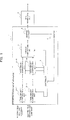
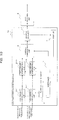
- Fig. 1 is a block diagram schematically illustrating an example of the configuration of a distortion compensating apparatus according to the first embodiment.
- a distortion compensating apparatus 1 depicted in Fig. 1 exemplarily includes fixed amount compensating units 2-1 through 2-N (where N is a natural number) and 3-1 through 3-N, a variable compensating unit 4, an adaptive equalizer 5, a monitor 6, and a controller 7.
- the fixed amount compensating units 2-1 through 2-N and the fixed amount compensating units 3-1 through 3-N are simply called the fixed amount compensating units 2 and the fixed amount compensating unit 3 when there is no requirement to discriminate one from the others.
- the first embodiment is described on the assumption that distortion in a waveform of a light signal which distortion is caused by wavelength dispersion of the light signal is to be compensated for. However, the present invention should by no means be limited to this assumption.
- the fixed amount compensating units 2 compensate for wavelength dispersion of the electric field real-axis component (e.g., the I-axis component in digital modulation) of a light signal input from an optical transmission path (not-illustrated) at respective fixed dispersion compensating amounts through digital signal processing.
- the electric field real-axis component e.g., the I-axis component in digital modulation
- the fixed amount compensating units 2-1 through 2-N are cascaded.
- the fixed amount compensating units 3 compensate for wavelength dispersion of the electric field imaginary-axis component (e.g., the Q-axis component in digital modulation) of the light signal input from the optical transmission path at respective fixed dispersion compensating amounts through digital signal processing.
- the electric field imaginary-axis component e.g., the Q-axis component in digital modulation
- the fixed amount compensating units 3-1 through 3-N are cascaded.
- An electric field imaginary-axis component compensated for by a fixed amount compensating unit 3-M is output to the downstream fixed amount compensating unit 3-(M+1), and the electric field imaginary-axis component compensated for by the fixed amount compensating unit 3-N is output to the variable compensating unit 4.
- the dispersion compensating amounts of the respective fixed amount compensating units 2-1 through 2-N may be the same, may be partially different, or may different from one another, and similarly those of the fixed amount compensating units 3-1 through 3-N may be the same, may be partially different, or may different from one another.
- the operation states of fixed amount compensating units 2 and 3 are individually on/off switching controlled. Such on/off switching maybe controlled by the controller 7 that is to be detailed below.
- the fixed amount compensating units 2 and 3 function as an example of a number of fixed amount compensating units which compensate for distortion in a waveform of a light signal that the distortion compensating apparatus 1 has received at respective fixed compensating amounts and the combination of operating states of which can be changed by on/off switching.
- variable compensating unit 4 compensates for wavelength dispersion of the electric field real-axis component and the electric field imaginary-axis component respectively input from fixed amount compensating units 2-N and 3-N at variable dispersion compensating amounts through digital signal processing.
- the signal compensated for by the variable compensating unit 4 is output to the adaptive equalizer 5.
- the variable compensating unit 4 is cascaded with the fixed amount compensating units 2 and 3, and is capable of compensating for the remaining wavelength dispersion in the light signal that the distortion compensating apparatus 1 has received after the compensation performed by the fixed amount compensating units 2 and 3.
- the dispersion compensating amount at which the variable compensating unit 4 compensates for wavelength dispersion may be controlled by, for example, the controller 7 to be detailed below.
- the fixed amount compensating units 2 and 3, and the variable compensating unit 4 each include a digital filter 22.
- each set of the fixed amount compensating units 2-1 and 3-1, ..., and the fixed amount compensating units 2-N and 3-N may be a common single form.
- the digital filters 22 may be Finite Impulse Response filters (e.g., complex FIR (Finite Impulse Response) filters) as depicted in the example Fig. 2 .
- the digital filters 22 of the present example should by no means be limited to FIR filters, but may be alternatively Infinite Impulse Response Filters (e.g., complex IIR (Infinite Impulse Response) filters).
- the digital filter 22 illustrated in the example Fig. 2 has the tap number of three, but the tap number of a filter should by no means be limited to three.
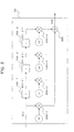
- the digital filter 22 illustrated in Fig. 2 exemplarily includes delay circuits 100-1 through 100-3, multiplexers 200-1 through 200-4, and an adder 300.
- the delay circuits 100-1 through 100-3 are sometimes represented by reference number 100 when there is no requirement to discriminated one from the others, and similarly, the multiplexers 200-1 through 200-4 are sometimes represented by reference number 200 when there is no requirement one from the others.
- a delay circuit 100 provides a given delay (e.g., ⁇ ) to an input signal.
- the delay circuit 100-1 provides a delay time ⁇ to an input signal S(t) and outputs the resultant signal S(t- ⁇ );
- the delay circuit 100-2 provides a delay time ⁇ to the output signal S(t- ⁇ ) from the delay circuit 100-1 and outputs the resultant signal S(t-2 ⁇ );
- the delay circuit 100-3 provides a delay time ⁇ to the output signal S(t-2 ⁇ ) from the delay circuit 100-2 and outputs the resultant signal S(t-3 ⁇ ).
- a multiplexer 200 multiplies an input signal and a coefficient pattern (a filter coefficient (e.g., c0 through c3)).
- a filter coefficient e.g., c0 through c3
- the multiplexer 200-1 multiplexes the input signal S (t) and the filter coefficient c0, and the multiplication result is output to the adder 300
- the multiplexer 200-2 multiplexes the output signal S(t- ⁇ ) from the delay circuit 100-1 and the filter coefficient c1, and the multiplication result is output to the adder 300
- the multiplexer 200-3 multiplexes the output signal S(t-2 ⁇ ) from the delay circuit 100-2 and the filter coefficient c2, and the multiplication result is output to the adder 300
- the multiplexer 200-4 multiplexes the output signal S(t-3 ⁇ ) from the delay circuit 100-3 and the filter coefficient c3, and the multiplication result is output to the adder 300.
- the adder 300 adds the output signals from the multiplexers 200-1 through 200-4, and then outputs an output signal R(t) representing the result of the addition.
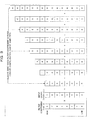
- the filter of Fig. 2 multiplies the input signal by the respective bit values of the filter coefficient from the LSB (Least Significant Bit) to the MSB (Most Significant Bit), adds the results of the multiplications depending on the bit positions of the filter coefficient, and outputs the result of the addition.
- calculating performed on the bit value "0" of the filter coefficient can be omitted, so that the circuit to carry out the corresponding calculating can be omitted.
- the results of the multiplication always include at least one bit string of "0" and therefore the circuit configuration corresponding to the bit string can be simplified.
- the hardware scale of the distortion compensating apparatus 1 can be reduced.
- the patterns (kinds) of filter coefficient can be less in number than the variable filter coefficients, and accordingly the number of wirings can be reduced in the digital filters.
- a digital filter having fixed filter coefficients has coefficient patterns less in kind than coefficient patterns possessed by a digital filter whose filter coefficients are variable, and can therefore make the filter circuit thereof small in size.
- the combination of filter coefficients of the fixed amount compensating units 2 and 3 may be selected so as to more simplify the filter circuits (i . e. , a combination including a relatively large number of bit values "0").
- the adaptive equalizer 5 compensates for the optical transmission path through adaptive equalizing processing (e.g., compensation for gain and/or phase) on the output signal from the variable compensating unit 4 in the time domain.
- adaptive equalizing processing e.g., compensation for gain and/or phase
- the adaptive equalizer 5 can compensate for wavelength dispersion remaining despite the compensation in the fixed amount compensating units 2 and 3 and the variable compensating unit 4.
- the signal subjected to equalizing processing by the adaptive equalizer 5 is then output to the monitor 6 and the data reproducing unit 8.
- the data reproducing unit 8 reproduces data through given demodulating and decoding processing on a digital signal which has been subjected to equalizing processing in the adaptive equalizer 5, and outputs the reproduced data.
- the monitor 6 measures a residual amount of wavelength dispersion (residual dispersion) remaining in the output signal from the adaptive equalizer 5. For example, the monitor 6 measures the wavelength dispersion (residual dispersion) that has not been compensated for by the fixed amount compensating units 2 and 3, the variable compensating unit 4, and the adaptive equalizer 5, and outputs the result of the measurement to the controller 7.
- the controller 7 changes a combination of operating states of the fixed amount compensating units 2 and 3 on the basis of distortion in the waveform caused by the optical transmission path through which the light signal propagates. For example, the controller 7 controls on/off switching of the operation of each of the fixed amount compensating units 2 and 3 such that the total compensating amount to be compensated for by switched-on fixed amount compensating units 2 and 3 becomes the closest to the amount of wavelength dispersion in the received light signal.
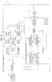
- a fixed amount compensating unit 2 (3) includes, for example, an input-end switch (SW) 21, a digital filter 22, an output-end switch (SW) 23, multiplexers 24 and 26, a sign controller 25, and a delay processor 27.
- the fixed amount compensating units 2 and 3 are formed into a single common form.
- the input-end switch 21 switches between a route to the digital filter 22 and a rout to the delay processor 27 and outputs an input electric field real-axis component and an input electric field imaginary-axis component to a switched route.
- the digital filter 22 multiplies an input component and a fixed filter coefficient, adds the results of the multiplication, and outputs the result of the addition.
- the digital filter 22 functions as an exemplary digital filter which regards one of the outputs from the input-end switch 21 as an input therein and which compensates for distortion in the waveform of a light signal at a fixed compensating amount.
- the output-end switch 23 selectively switches between an input from the digital filter 22 and an input from the delay processor 27 and outputs the selected input to the output end of the fixed amount compensating unit 2 (3).
- the multiplexer 24 multiplies an electric field imaginary-axis component from the input-end switch 21 and a control signal from the sign controller 25, and outputs the result of the multiplication to the digital filter 22.
- the multiplexer 26 multiplies a compensated electric field imaginary-axis component from the digital filter 22 and a control signal from the sign controller 25, and outputs the result of the multiplication to the output-end switch 23.
- the sign controller 25 inverts the plus and the minus of the dispersion compensating amount of the fixed amount compensating unit 2 (3) under the control of the controller 7. For example, when the fixed compensating amount of the fixed amount compensating unit 2 (3), including the sign controller 25, is a plus value, the sign controller 25 outputs the digit "1" to the multiplexer 24 and the multiplexer 26. Conversely, when the fixed compensating amount is a minus value, the sign controller 25 outputs the digit "-1" to the multiplexer 24 and the multiplexer 26.
- the sign controller 25 included in the same fixed amount compensating unit 2 (3) keeps the sign of an imaginary component of a complex signal input into and output from the fixed amount compensating unit 2 (3) unchanged in the illustrated embodiment.
- the sign controller 25 inverts the sign of the imaginary component.
- the sign controller 25 inverts the sign of the electric field imaginary-axis component that is to input into the digital filter 22 and the sign of the compensated electric-field imaginary-axis component output from the digital filter 22.
- This configuration allows the digital filter 22 to obtain two kinds (plus and minus) of dispersion compensating amount from each individual filter coefficient.
- the delay processor 27 introduces delay into an electric field real-axis component and an electric field imaginary-axis component from the input-end switch 21, and outputs the delayed components to the output-end switch 23.
- the delay processor 27 of the illustrated example functions as an exemplary delay processor that receives the other output from the input-end switch 21 as the input therein and that performs delay processing on the input.
- the fixed amount compensating unit 2 (3) having the above configuration selectively switches an output destination from the input-end switch 21 and an input source into the output-end switch 23 under on/off switching control of the controller 7. For example, when the fixed amount compensating unit 2 (3) is switched on, the controller 7 switches the input-end switch 21 and the output-end switch 23 such that the result of processing at the digital filter 22 is output. On the other hand, when the fixed amount compensating unit 2 (3) is switched off, the controller 7 switches the input-end switch 21 and the output-end switch 23 such that the result of processing at the delay processor 27 is output.
- the mechanism for the on/off switching may be disposed at the exterior of the fixed amount compensating unit 2 (3).
- the fixed amount compensating unit 2 (3) can switch the on/off of its operation state with the configuration illustrated in the example of Fig. 5 .
- the controller 7 sets the filter coefficient of the digital filter 22 to a given value.
- the controller 7 sets the filter coefficient of the digital filter 22 to a coefficient pattern (a filter coefficient) which makes the same fixed amount compensating unit 2 (3) switched off.
- the middle bit of the filter coefficient of the digital filter 22 is set to be "1" and the remaining bits are set to be "0".
- the controller 7 variably controls the compensating amount of the variable compensating unit 4 on the basis of the distortion in the wavelength of the signal light and the compensating amounts of the fixed amount compensating units 2 and 3. For example, the controller 7 controls the variable compensating amount of the variable compensating unit 4 such that the amount of wavelength dispersion remaining after the compensation in the fixed amount compensating units 2 and 3 can be compensated for. In other words, the controller 7 variably controls the compensating amount of the variable compensating unit 4 in order to compensate for wavelength dispersion remaining after the processing by the adaptive equalizer 5.
- the controller 7 can determine the amount of dispersion compensated for in the variable compensating unit 4 to be the amount equal to the difference obtained by subtracting the total amount of compensating by the fixed amount compensating units 2 and 3 from the amount of wavelength dispersion caused by the optical transmission path.
- controller 7 may control on/off switching of the operation states of each of the fixed amount compensating units 2 and 3 and variably control the compensating amount of the variable compensating unit 4 such that a given amount of wavelength dispersion is compensated for, or may carry out the above control on the basis of the result of measurement by the monitor 6.
- the controller 7 can control the fixed amount compensating units 2 and 3 and the variable compensating unit 4 such that an amount of wavelength dispersion given by the user is compensated for at the beginning of the communication, and when the wavelength dispersion varies during the communication, can control the compensation so as to keep up with the variation in the wavelength dispersion.
- Fig. 6 is a flow diagram denoting an example of a succession of procedural steps performed by the distortion compensating apparatus 1.
- Fig. 7 is a block diagram schematically illustrating an example of the configuration of the distortion compensating apparatus 1 of the illustrated example. The example of Fig.
- the compensating amounts of the fixed amount compensating units 2-1 through 2-3 and the variable compensating unit 4 are not limited to those in this example, and therefore the dispersion compensating amounts of the fixed amount compensating units 2-1 through 2-3 may be different one from the others.
- the distortion compensating apparatus 1 of this example obtains a dispersion compensating amount (target dispersion compensating amount) given by the user and other (step S1) as denoted in Fig. 6 .
- the target dispersion compensating amount is set to be 2300 ps/nm.
- the unit "ps" represents an amount of width of the light pulse and the unit “nm” represents a width of spectrum of a light signal.
- the controller 7 switches one or more fixed amount compensating units 2 as many as the quotient (integer) obtained by dividing the target dispersion compensating amount by the dispersion compensating amount (fixed filter dispersion amount) of the fixed amount compensating units 2 on and switches the remaining fixed amount compensating units 2 off (step S2).
- two fixed amount compensating units 2-2 and 2-3 are switched on and the single remaining fixed amount compensating unit 2-1 is switched off.
- the position of fixed amount compensating units 2 that are to be switched on (or switched off) are not limited to the above example.
- the controller 7 may control on/off switching of each fixed amount compensating unit 2 such that the total dispersion compensating amount of one or more switched-on fixed amount compensating units 2 becomes the closest to but dose not exceed the target dispersion compensating amount.
- the controller 7 variably controls the filter coefficient of the digital filter possessed by the variable compensating unit 4 such that the dispersion compensating amount of the variable compensating unit (variable filter) 4 is difference obtained by subtracting the product of compensating amount of a single fixed amount compensating unit (fixed filter) 2 and the number of switched-on fixed amount compensating units 2 from the target dispersion amount (step S3).
- the fixed amount compensating units 2 and the variable compensating unit 4 can compensate for wavelength dispersion as much as the target dispersion compensating amount given.
- the signal whose dispersion has been compensated for by fixed amount compensating units 2 and the variable compensating unit 4 is subjected to equalizing processing in the adaptive equalizer 5 and is further measured for a residual dispersion amount by the monitor 6 (step S4).
- the result of the measurement by the monitor 6 is output to the controller 7, which determines whether or not the amount of the measured residual dispersion can be compensated for by a signal fixed amount compensating unit 2 (i.e., the amount is 1000 ps/nm in the example of Fig. 7 ) or more (step S5).
- a signal fixed amount compensating unit 2 i.e., the amount is 1000 ps/nm in the example of Fig. 7
- step S5 determines whether or not the amount of the measured residual dispersion can be compensated for by a signal fixed amount compensating unit 2 (i.e., the amount is 1000 ps/nm in the example of Fig. 7 ) or more (step S5).
- the controller 7 changes the number of switched-on fixed amount compensating units 2 such that the amount of dispersion to be compensated for by the variable compensating unit 4 becomes the minimum (step S6).
- the controller 7 can further switch the fixed amount compensating unit 2-1 on and concurrently change the dispersion compensating amount of the variable compensating unit 4 to be 500 ps/nm.
- the controller 7 can switch the fixed amount compensating unit 2-2 or 2-3 off and change the dispersion compensating amount of the variable compensating unit 4 to be 200 ps/nm.
- the controller 7 may change the number of switched-on fixed amount compensating units 2 such that the amount of dispersion to be compensated for by the variable compensating unit 4 becomes the minimum. Assuming that the residual dispersion is 800 ps/nm, the sum of the amount of the residual dispersion and the dispersion compensating amount (300 ps/nm) of the variable compensating unit 4 is 1100 ps/nm, which is larger than a dispersion amount (1000 ps/nm) that a single fixed amount compensating unit 2 can compensated for. In this case, the controller 7 may further switch the remaining fixed amount compensating unit 2-1 on and change the dispersion compensating amount of the variable compensating unit 4 to 100 ps/nm.
- the controller 7 changes the dispersion compensating amount of the variable compensating unit 4 depending on the amount of the residual dispersion (step S7). For example, assuming that the amount of residual dispersion is 200 ps/nm, the controller 7 can change the dispersion compensating amount of the variable compensating unit 4 from 300 nm/ps to 500 ps/nm without changing the number of switched-on fixed amount compensating units 2.
- the controller 7 may carry out control to change the number of switched-on fixed amount compensating units 2 on the basis of the amount of residual dispersion and the dispersion compensating amount set in the variable compensating unit 4. Assuming the residual dispersion is -400 ps/nm, the controller 7 may switch the fixed amount compensating unit 2-2 or 2-3 off and concurrently change the dispersion compensating amount of the variable compensating unit 4 to 900 ps/nm.
- the distortion compensating apparatus 1 of this example flexibly compensates for distortion (e.g., wavelength distortion) in waveform of a light signal through adaptive on/off switching the fixed filters (i.e., the fixed amount compensating units 2 and 3) smaller in circuit scale than a variable filter. It is therefore possible to reduce the hardware scale of the distortion compensating apparatus 1.
- distortion e.g., wavelength distortion
- the distortion compensating apparatus 1 of the illustrated example may omit the variable compensating unit 4.
- the distortion compensating apparatus 1 can compensate for a target dispersion compensating amount by controlling the combination of operating states of a number of fixed amount compensating units 2 (3).
- the optical transmitting and receiving system of Fig. 8 exemplarily includes an optical transmitting apparatus 50 and an optical receiving apparatus 40.
- the optical receiving apparatus 40 exemplarily includes a PBS (Polarizing Beam Splitter) 30, a local light emitting unit 31, a PBS 32, 90-degree hybrids 33-1 and 33-2, O/Es (optical/electrical convertors) 34-1 through 34-4, ADCs (Analog-to-Digital Converters) 35-1 through 35-4, and the distortion compensating apparatus 1.
- a 90-degree hybrid is represented by the reference number 33 when the 90-degree hybrids 33-1 and 33-2 are not discriminated from each other.
- the PBS 30 divides an input signal light input from the optical transmitting apparatus 50 through the optical transmission path into the X polarization and the Y polarization that are orthogonal to each other.
- the X-polarized light by the PBS 30 is output to the 90-degree hybrid 33-1 and the Y-polarized light obtained through the division by the PBS 30 is output to the 90-degree hybrid 33-2.
- the local light emitting unit 31 is semiconductor laser that oscillates at the same frequency as or a different frequency from that of the input signal light.
- the light locally emitted from the local light emitting unit 31 is output to the PBS 32.
- the PBS 32 is exemplified by an optical branching filter that maintains a plane of polarization and bifurcates the locally emitted light from the local light emitting unit 31.
- the bifurcated light components from the PBS 32 are output one to each of the 90-degree hybrids 33-1 and 33-2.
- the 90-degree hybrid 33-1 causes the X-polarized divided light input from the PBS 30 and one of the bifurcated light components input from PBS 32 to have a phase difference of 90 degrees and outputs the X polarization and the bifurcated light component to the O/Es 34-1 and 34-2.
- the 90-degree hybrid 33-2 causes the Y-polarized divided light input from the PBS 30 and the other bifurcated light component input from PBS 32 to have a phase difference of 90 degrees and outputs the Y polarization and the bifurcated light component to the O/Es 34-3 and 34-4.
- the O/Es 34-1 through 34-4 converts signal light from the 90-degree hybrid 33 into an electrical signal and outputs the electrical signal to the ADCs 35-1 through 35-4.
- the O/Es 34 of the illustrated example have a function for heterodyne detection or homodyne detection.
- the ADCs 35-1 through 35-4 convert analog electrical signals from the O/Es 34 into digital signals.
- the ADC 35-1 outputs an X-polarized electric field real-axis component (XI) to the fixed amount compensating unit 2-1 of the distortion compensating apparatus 1;
- the ADC 35-2 outputs an X-polarized electric field imaginary-axis component (XQ) to the fixed amount compensating unit 3-1 of the distortion compensating apparatus 1;
- the ADC 35-3 outputs a Y-polarized electric field real-axis component (YI) to the fixed amount compensating unit 2-1 of the distortion compensating apparatus 1;
- the ADC 35-4 outputs a Y-polarized electric field imaginary-axis component (YQ) to the fixed amount compensating unit 3-1 of the distortion compensating apparatus 1.
- the distortion compensating apparatus 1 Upon receipt of the electric field real-axis components and the electric field imaginary-axis components from the ADCs, the distortion compensating apparatus 1 compensates for distortion, such as wavelength dispersion, in a waveform of signal light through the above-described procedure, and then reproduces and outputs the compensated data.
- distortion such as wavelength dispersion
- the distortion compensating apparatus 1 can be applied to an optical receiving apparatus 40 that adopts a coherent receiving scheme, for example. It is therefore possible to reduce the hardware scale of the optical receiving apparatus 40.
- the distortion compensating apparatus 1 of this example is included in the optical receiving apparatus 40 having a polarized light diversity configuration having 90-degree hybrids 33 and O/Es 34 are doubled in number.
- an optical receiving apparatus 40A that adopts a scheme of receiving single polarized light may be used.
- Fig. 9 depicts an example of an optical transmitting and receiving system including the distortion compensating apparatus 1 of the illustrated example.
- the optical transmitting and receiving system of Fig. 9 includes the optical transmitting apparatus 50 and the optical receiving apparatus 40A which adopts a scheme of receiving single polarized light.
- the optical receiving apparatus 40A exemplarily includes a local light emitting unit 31, a 90-degree hybrid 33, O/Es 34-1 and 34-2, ADCs 35-1 and 35-2, and the distortion compensating apparatus 1.
- the local light emitting unit 31 is semiconductor laser that oscillates at the same frequency as or a different frequency from that of the input signal light.
- the locally emitted light from the local light emitting unit 31 is output to the 90-degree hybrid 33.
- the 90-degree hybrid 33 causes an input signal light input from the optical transmitting apparatus 50 through the optical transmission path and the locally emitted light from the local light emitting unit 31 to have a phase difference of 90 degrees and outputs the input signal light and the locally emitted light to the O/Es 34-1 and 34-2.
- the O/Es 34-1 and 34-2 convert the signal light from the 90-degree hybrid 33 into an electrical signal, and outputs the electrical signal to the ADCs 35-1 and 35-2.
- the O/Es of the present example have a function of heterodyne detection or homodyne detection.
- the ADCs 35-1 and 35-2 convert analog electrical signals from the O/E 34 to digital signals.
- the ADC 35-1 outputs an electric field real-axis component (I) of the input signal light to the fixed amount compensating unit 2-1 of the distortion compensating apparatus 1 and the ADC 35-2 outputs the electric field imaginary-axis component (Q) of the input signal light to the fixed amount compensating unit 3-1 of the distortion compensating apparatus 1.
- the distortion compensating apparatus 1 Upon receipt of the electric field real-axis component and the electric field imaginary-axis component from ADCs, the distortion compensating apparatus 1 compensates for distortion, such as wavelength dispersion, in a waveform of signal light through the above-described procedure, and then reproduces and outputs the compensated data.
- distortion such as wavelength dispersion
- the distortion compensating apparatus 1 can also be applied to the optical receiving apparatus 40A which adopts a scheme of receiving single polarized light. Also in this application, it is possible to reduce the hardware scale of the optical receiving apparatus 40A.
- each of the fixed amount compensating units 2 and 3 has a single kind of dispersion compensating amount (i.e., a single kind of filter coefficient).
- the dispersion compensating amount of each of the fixed amount compensating units 2 and 3 is selected (switched) from a number of kinds of dispersion compensating amount.
- Fig. 10 is a block diagram schematically illustrating an example of the configuration of the distortion compensating apparatus 1A of this example.
- the distortion compensating apparatus 1A of Fig. 10 exemplarily includes fixed amount compensating units 2-1 through 2-N and 3-1 through 3-N, a variable compensating unit 4, an adaptive equalizer 5, a monitor 6, a controller 7, and a filter coefficient switch 9.
- the fixed amount compensating units 2-1 through 2-N and 3-1 through 3-N, the variable compensating unit 4, the adaptive equalizer 5, the monitor 6, the controller 7, and the data reproducing unit 8 are same in function as those illustrated in Fig 1 .
- Each fixed amount compensating unit 2 includes a digital fil ter 22A having a number of kinds of coefficient pattern (filter coefficient).
- the filter coefficient switch 9 selects one filter coefficient from a number of filter coefficients possessed by the digital filters 22A (switches a filter coefficient).
- the digital filter 22A of Fig. 11 exemplarily includes delay circuits 100-1 through 100-3, multiplexer 200-1 through 200-4, and an adder 300, which are same in function as those illustrated in Fig 2 .
- bit strings of the two filter coefficients are the same except for the fourth bit and the seventh bit
- switching between the two filter coefficients can be accomplished by a configuration in which the fourth bit and the seventh bit are set to be variable while the remaining bits are set to be fixed.
- this example switches the values of the two variable bits and thereby allows a single digital filter 22A to have a number of patterns of compensating amounts.
- the presence of the fixed bits makes it possible to reduce the circuit size as compared with the cases where a variable filter is used, and consequently the hardware scale of the fixed amount compensating unit 2 (3) can be reduced.
- Fig. 11 assumes that the digital filter 22A possesses two patterns of filter coefficients, but the digital filter 22A may alternatively have more than two filter coefficient patterns.
- the filter coefficient patterns have at least one fixed bit, the circuit scale can be reduced as compared with a variable filter having filter coefficient same in bit number.
- Such a configuration allows a single fixed amount compensating unit 2(3) to realize a number of dispersion compensating amounts classified into, for example, "no" dispersion compensation, "small” dispersion compensation, “medium” dispersion compensation, and "large” dispersion compensation.
- the distortion compensating apparatus 1A of this example can ensure the same effects of the foregoing example, further improving the capability of dispersion compensation.
- a distortion compensating apparatus 1B of this example can compensate for non-linear distortion in a light signal.
- Fig. 12 is a block diagram schematically illustrating an example of the configuration of the distortion compensating apparatus 1B of this modification.
- the distortion compensating apparatus 1B of Fig. 12 exemplarily includes fixed amount compensating units 2-1 through 2-N and 3-1 through 3-N, a variable compensating unit 4, an adaptive equalizer 5, a monitor 6, a controller 7, a filter coefficient switch 9, and non-linear compensating units 10.
- the fixed amount compensating units 2-1 through 2-N and 3-1 through 3-N, the variable compensating unit 4, the adaptive equalizer 5, the monitor 6, the controller 7, the data reproducing unit 8, and the filter coefficient switch 9 are same in function as those illustrated in Fig 10 .
- the non-linear compensating units 10 compensate for non-linear distortion in a light signal from an optical transmission path (not illustrated).
- the non-linear compensating units 10 may be alternately cascaded with the fixed amount compensating units 2 and 3 as illustrated in Fig. 12 .
- the distortion compensating apparatus 1B of this example can compensate for wavelength dispersion in a light signal and concurrently compensate for non-linear distortion in the light signal.
- the distortion compensating apparatus 1B may include one or more other devices, such as compensating units, in addition to or as substitutes for the non-linear compensating units 10.
- the distortion compensating apparatus 1B of this example can ensure the same effects of the foregoing first embodiment and first modification, further compensating for non-linear distortion in a light signal.
- the elements included in and the processes performed in the above distortion compensating apparatuses 1, 1A, and 1B can be partially discarded and/or combined according to the requirements.
- At least one fixed amount compensating unit 2(3) and the variable compensating unit 4 are cascaded in this order, but the position of the variable compensating unit 4 and the number of variable compensating units 4 may be modified.
- the variable compensating unit 4 may be disposed ahead of the fixed amount compensating units 2(3), or a number of variable compensating units 4 may be alternated with blocks including one (or more) fixed amount compensating units 2(3).
- the distortion compensating apparatus 1 and the optical receiving apparatus 40 (40A) may be applied to optical communication systems adopting various modulations, such as DPSK (Differential Phase Shift Keying), QPSK (Quadrature Phase Shift Keying), SPSK (Symmetric Phase Shift Keying), and 16QAM (16 Quadrature Amplitude Modulation.
- DPSK Different Phase Shift Keying
- QPSK Quadratture Phase Shift Keying
- SPSK Symmetric Phase Shift Keying
- 16QAM 16 Quadrature Amplitude Modulation.
- the distortion compensating apparatus 1 and the optical receiving apparatus 40(40A) may be applied to optical communication systems of the above modulation methods using polarized multiplexed light signals.
Landscapes
- Physics & Mathematics (AREA)
- Electromagnetism (AREA)
- Engineering & Computer Science (AREA)
- Computer Networks & Wireless Communication (AREA)
- Signal Processing (AREA)
- Optical Communication System (AREA)
- Filters That Use Time-Delay Elements (AREA)
- Amplifiers (AREA)
Abstract
Description
- The embodiment discussed herein is related to a distortion compensating apparatus, an optical receiving apparatus, and an optical transmitting and receiving system. The distortion compensating apparatus is one that compensates for distortion in a waveform of a light signal through digital processing.
- One of the methods to realize large-capacity optical communication is to increase the optical transmission speed.
- However, it is known that simple increase in the optical transmission speed result in generation of distortion in a waveform which distortion is caused by wavelength dispersion of the optical transmission path (e.g., an optical fiber). This restricts the optical transmission.
- The speed of light propagating through an optical transmission path varies with the wavelength (frequency) of the light, and such a variation widens the pul se of light, which is called the effect of wavelength dispersion of an optical transmission path. When an optical transmission path has wavelength dispersion, the presence of a number of frequency components in a light pulse, which frequency components are different in transmission speed, causes transmission light to have distortion in a waveform depending of the dispersion amount (the product of dispersion and distance).
- When such distortion in a waveform is not compensated for, the amount of dispersion tolerant in optical transmission has a limit value, which is in inverse proportion ratio to approximate square of transmission speed of a signal. That means the tolerant limit becomes smaller in accordance with increase in transmission speed. In other words, a higher transmission speed of a signal makes the optical transmission less possible.
- For example, in the cases where the bit rate of a transmission signal is about 2.5 Gbps, the light pulse has a relatively narrow spectrum width and therefore the pulse width is small, which has a less possibility in generation of inter symbol interference unless ultra long-haul transmission.
- However, in the cases where the bit rate (speed) of a transmission signal is 10 Gbps or 40 Gbps, the spectrum width of the light pulse is wide as compared with that of a transmission signal of 2.5 Gbps and therefore the same amount of dispersion results in a larger pulse width. In the above cases, the narrow distance between light pulses increases the possibility of the generation of a small pulse spread to generate inter symbol interference.
- For the above, it is preferable that wavelength dispersion caused by an optical transmission line is compensated for in accordance with increase of the bit rate of a transmission signal to 2.5 Gbps, 10 Gbps, 40 Gbps, and 100 Gbps.
- There have been known the techniques of the
non-patent references 1 through 4 as exiting techniques of dispersion compensation. - For example, one of the known methods converts a modulated complex optical electric field into a digital signal and compensates for distortion caused by wavelength dispersion of signal light through digital complex-filter processing (see Non-patent
reference 1 below). - In order to reduce the circuit scale of a distortion compensating circuit, another method teaches that signal light is converted from a time domain to a frequency domain and wavelength dispersion is compensated for in a frequency domain (see Non-Patent
reference 2 below). - Further, there have been known a method of monitoring an amount of wavelength dispersion (see Non-Patent
reference 3 below) and a method of compensating for non-linear distortion (see Non-Patent Reference 4). - Non-Patent Reference 1: G. Charlet et al., "Transmission of 81 channels at 40Gbit/s over a Transpacific-Distance Erbium-only Link, using PDM-BPSK Modulation, Coherent Detection, and a new large effective area fibre." ECOC 2008, Brussels, Belgium, September 21-25, 2008, TH.3.E.3, Vol.7, p.29-30
- Non-Patent Reference 2: B. Spinnler et al., "Adaptive Equalizer Complexity in Coherent Optical Receivers┘, ECOC 2008, Brussels, Belgium, September 21-25, 2008, We.2.E.4, Vol.3, p.127-128
- Non-Patent Reference 3: F.N. Hauske et al., "Optical Performance Monitoring from FIR Filter Coefficients in Coherent Receivers", OFC/NFOEC 2008
- Non-Patent Reference 4: Kazuo Kikuchi, "Electronic Post-compensation for Nonlinear Phase Fluctuations in a 1000-km 20-Gbit/s Optical Quadrature Phase-Shift Keying Transmission System Using the Digital Coherent Receiver" OPTICS EXPRESS, January 21, 2008, Vol.16, No.2, p.889-896
- However, compensation for the above wavelength dispersion requires a long filter corresponding to a light signal received by the dispersion compensating apparatus. As a consequence, the hardware scale of the distortion compensating apparatus becomes large.
-
- (1) According to an aspect of the embodiment, an apparatus includes a distortion compensating apparatus for compensating for distortion in a waveform of a received light signal through digital signal processing, the distortion compensating apparatus including a plurality of fixed amount compensating units which compensate for the distortion in the waveform at respective given compensating amounts, wherein a combination of operating states of the plurality of fixed amount compensating units is changed by on/off switching of each of the plurality of fixed amount compensating units, and the plurality of fixed amount compensating units are cascaded.
- (2) According to an aspect of the embodiment, an apparatus includes an optical receiving apparatus including the above dispersion compensating apparatus.
- (3) According to an aspect of the embodiment, an apparatus includes an optical transmitting and receiving system including the above dispersion compensating apparatus.
- It is possible to reduce the hardware scale of the distortion compensating apparatus.
-
-
Fig. 1 is a block diagram schematically illustrating an example of the configuration of a distortion compensating apparatus according to a first embodiment; -
Fig. 2 is a block diagram schematically illustrating an example of a digital filter; -
Fig. 3 is a diagram depicting an example of a method of simplifying the circuit configuration of the digital filter ofFig. 2 ; -
Fig. 4 is a block diagram illustrating an example of a fixed amount compensating unit ofFig. 1 ; -
Fig. 5 is a block diagram illustrating another example of a fixed amount compensating unit ofFig. 1 ; -
Fig. 6 is a flow diagram denoting a succession of procedural steps performed by the distortion compensating apparatus ofFig. 1 ; -
Fig. 7 is a block diagram schematically illustrating an example of the configuration of the distortion compensating apparatus ofFig. 1 ; -
Fig. 8 is a block diagram schematically illustrating an example of an optical transmitting and receiving system including the distortion compensating apparatus ofFig. 1 ; -
Fig. 9 is a block diagram schematically illustrating another example of an optical transmitting and receiving system including the distortion compensating apparatus ofFig. 1 ; -
Fig. 10 is a block diagram schematically illustrating an example of a distortion compensating apparatus according to a first modification; -
Fig. 11 is a diagram denoting a method of switching a filter coefficient of a fixed amount compensating unit ofFig. 10 ; and -
Fig. 12 is a block diagram schematically illustrating an example of a distortion compensating apparatus according to a second modification. - Hereinafter, exemplary embodiments will be described with reference to accompanying drawings. The following exemplary embodiments are merely examples and do not intend to exclude various modifications and variations to the proposed method and/or apparatus that are not specifically described herein. Rather, various modifications or variations may be made to the embodiments (for example, by combining the exemplary embodiments) without departing from the scope and spirit of the proposed method and/or apparatus.
-
Fig. 1 is a block diagram schematically illustrating an example of the configuration of a distortion compensating apparatus according to the first embodiment. - A
distortion compensating apparatus 1 depicted inFig. 1 exemplarily includes fixed amount compensating units 2-1 through 2-N (where N is a natural number) and 3-1 through 3-N, a variable compensatingunit 4, anadaptive equalizer 5, amonitor 6, and acontroller 7. The fixed amount compensating units 2-1 through 2-N and the fixed amount compensating units 3-1 through 3-N are simply called the fixedamount compensating units 2 and the fixedamount compensating unit 3 when there is no requirement to discriminate one from the others. The first embodiment is described on the assumption that distortion in a waveform of a light signal which distortion is caused by wavelength dispersion of the light signal is to be compensated for. However, the present invention should by no means be limited to this assumption. - Here, the fixed
amount compensating units 2 compensate for wavelength dispersion of the electric field real-axis component (e.g., the I-axis component in digital modulation) of a light signal input from an optical transmission path (not-illustrated) at respective fixed dispersion compensating amounts through digital signal processing. - The fixed amount compensating units 2-1 through 2-N are cascaded. An electric field real-axis component compensated for by a fixed amount compensating unit 2-M (where M=1, ..., N-1) is output to the downstream fixed amount compensating unit 2- (M+1), and the electric field real-axis component compensated for by the fixed amount compensating unit 2-N is output to the
variable compensating unit 4. - The fixed
amount compensating units 3 compensate for wavelength dispersion of the electric field imaginary-axis component (e.g., the Q-axis component in digital modulation) of the light signal input from the optical transmission path at respective fixed dispersion compensating amounts through digital signal processing. - Similarly to the fixed amount compensating units 2-1 through 2-N, the fixed amount compensating units 3-1 through 3-N are cascaded. An electric field imaginary-axis component compensated for by a fixed amount compensating unit 3-M is output to the downstream fixed amount compensating unit 3-(M+1), and the electric field imaginary-axis component compensated for by the fixed amount compensating unit 3-N is output to the
variable compensating unit 4. - Here, the dispersion compensating amounts of the respective fixed amount compensating units 2-1 through 2-N may be the same, may be partially different, or may different from one another, and similarly those of the fixed amount compensating units 3-1 through 3-N may be the same, may be partially different, or may different from one another.
- The operation states of fixed
amount compensating units controller 7 that is to be detailed below. - In other words, the fixed
amount compensating units distortion compensating apparatus 1 has received at respective fixed compensating amounts and the combination of operating states of which can be changed by on/off switching. - The variable compensating
unit 4 compensates for wavelength dispersion of the electric field real-axis component and the electric field imaginary-axis component respectively input from fixed amount compensating units 2-N and 3-N at variable dispersion compensating amounts through digital signal processing. The signal compensated for by the variable compensatingunit 4 is output to theadaptive equalizer 5. - The variable compensating
unit 4 is cascaded with the fixedamount compensating units distortion compensating apparatus 1 has received after the compensation performed by the fixedamount compensating units variable compensating unit 4 compensates for wavelength dispersion may be controlled by, for example, thecontroller 7 to be detailed below. - Here, the fixed
amount compensating units unit 4 each include adigital filter 22. Alternatively, each set of the fixed amount compensating units 2-1 and 3-1, ..., and the fixed amount compensating units 2-N and 3-N may be a common single form. In such a configuration, thedigital filters 22 may be Finite Impulse Response filters (e.g., complex FIR (Finite Impulse Response) filters) as depicted in the exampleFig. 2 . However, thedigital filters 22 of the present example should by no means be limited to FIR filters, but may be alternatively Infinite Impulse Response Filters (e.g., complex IIR (Infinite Impulse Response) filters). Thedigital filter 22 illustrated in the exampleFig. 2 has the tap number of three, but the tap number of a filter should by no means be limited to three. - The
digital filter 22 illustrated inFig. 2 exemplarily includes delay circuits 100-1 through 100-3, multiplexers 200-1 through 200-4, and anadder 300. The delay circuits 100-1 through 100-3 are sometimes represented by reference number 100 when there is no requirement to discriminated one from the others, and similarly, the multiplexers 200-1 through 200-4 are sometimes represented byreference number 200 when there is no requirement one from the others. - A delay circuit 100 provides a given delay (e.g., τ) to an input signal. In the example of
Fig. 2 , the delay circuit 100-1 provides a delay time τ to an input signal S(t) and outputs the resultant signal S(t-τ); the delay circuit 100-2 provides a delay time τ to the output signal S(t-τ) from the delay circuit 100-1 and outputs the resultant signal S(t-2τ); and the delay circuit 100-3 provides a delay time τ to the output signal S(t-2τ) from the delay circuit 100-2 and outputs the resultant signal S(t-3τ). - A
multiplexer 200 multiplies an input signal and a coefficient pattern (a filter coefficient (e.g., c0 through c3)). In the example ofFig. 2 , the multiplexer 200-1 multiplexes the input signal S (t) and the filter coefficient c0, and the multiplication result is output to theadder 300; the multiplexer 200-2 multiplexes the output signal S(t-τ) from the delay circuit 100-1 and the filter coefficient c1, and the multiplication result is output to theadder 300; the multiplexer 200-3 multiplexes the output signal S(t-2τ) from the delay circuit 100-2 and the filter coefficient c2, and the multiplication result is output to theadder 300; and the multiplexer 200-4 multiplexes the output signal S(t-3τ) from the delay circuit 100-3 and the filter coefficient c3, and the multiplication result is output to theadder 300. - The
adder 300 adds the output signals from the multiplexers 200-1 through 200-4, and then outputs an output signal R(t) representing the result of the addition. - Here, as denoted in the example of
Fig. 3 , when a fixed filter coefficient ("01101010") and a variable input signal ("10110001") are to be multiplied, the filter ofFig. 2 multiplies the input signal by the respective bit values of the filter coefficient from the LSB (Least Significant Bit) to the MSB (Most Significant Bit), adds the results of the multiplications depending on the bit positions of the filter coefficient, and outputs the result of the addition. - Specifically, in the example of
Fig. 3 , the result "00000000" of multiplication of the LSB of the fixed filter coefficient and the variable input signal, the result "10110001" of multiplication of the second bit of the fixed filter coefficient and the variable input signal, the result "10110001" of multiplication of the third bit of the fixed filter coefficient and the variable input signal, the result "00000000" of multiplication of the fourth bit of the fixed filter coefficient and the variable input signal, the result "10110001" of multiplication of the fifth bit of the fixed filter coefficient and the variable input signal, the result "00000000" of multiplication of the sixth bit of the fixed filter coefficient and the variable input signal, the result "10110001" of multiplication of the seventh bit of the fixed filter coefficient and the variable input signal, and the result "00000000" of multiplication of the MSB of the fixed filter coefficient and the variable input signal are added depending on each bit position (digit). - In the above calculation, calculating performed on the bit value "0" of the filter coefficient can be omitted, so that the circuit to carry out the corresponding calculating can be omitted. For example, when a filter coefficient is fixed and partially includes the bit of "0", the results of the multiplication always include at least one bit string of "0" and therefore the circuit configuration corresponding to the bit string can be simplified. As a consequence, the hardware scale of the
distortion compensating apparatus 1 can be reduced. - When the filter coefficients are fixed, the patterns (kinds) of filter coefficient can be less in number than the variable filter coefficients, and accordingly the number of wirings can be reduced in the digital filters. In other words, since a digital filter having fixed filter coefficients has coefficient patterns less in kind than coefficient patterns possessed by a digital filter whose filter coefficients are variable, and can therefore make the filter circuit thereof small in size. In addition, the combination of filter coefficients of the fixed
amount compensating units - Here, the
adaptive equalizer 5 compensates for the optical transmission path through adaptive equalizing processing (e.g., compensation for gain and/or phase) on the output signal from the variable compensatingunit 4 in the time domain. In other words, theadaptive equalizer 5 can compensate for wavelength dispersion remaining despite the compensation in the fixedamount compensating units unit 4. The signal subjected to equalizing processing by theadaptive equalizer 5 is then output to themonitor 6 and thedata reproducing unit 8. - The
data reproducing unit 8 reproduces data through given demodulating and decoding processing on a digital signal which has been subjected to equalizing processing in theadaptive equalizer 5, and outputs the reproduced data. - The
monitor 6 measures a residual amount of wavelength dispersion (residual dispersion) remaining in the output signal from theadaptive equalizer 5. For example, themonitor 6 measures the wavelength dispersion (residual dispersion) that has not been compensated for by the fixedamount compensating units unit 4, and theadaptive equalizer 5, and outputs the result of the measurement to thecontroller 7. - The
controller 7 changes a combination of operating states of the fixedamount compensating units controller 7 controls on/off switching of the operation of each of the fixedamount compensating units amount compensating units - As illustrated in
fig. 4 , a fixed amount compensating unit 2 (3) includes, for example, an input-end switch (SW) 21, adigital filter 22, an output-end switch (SW) 23,multiplexers sign controller 25, and adelay processor 27. In the example illustrated inFig. 4 , the fixedamount compensating units - The input-
end switch 21 switches between a route to thedigital filter 22 and a rout to thedelay processor 27 and outputs an input electric field real-axis component and an input electric field imaginary-axis component to a switched route. - The
digital filter 22 multiplies an input component and a fixed filter coefficient, adds the results of the multiplication, and outputs the result of the addition. Namely, thedigital filter 22 functions as an exemplary digital filter which regards one of the outputs from the input-end switch 21 as an input therein and which compensates for distortion in the waveform of a light signal at a fixed compensating amount. - The output-
end switch 23 selectively switches between an input from thedigital filter 22 and an input from thedelay processor 27 and outputs the selected input to the output end of the fixed amount compensating unit 2 (3). - The
multiplexer 24 multiplies an electric field imaginary-axis component from the input-end switch 21 and a control signal from thesign controller 25, and outputs the result of the multiplication to thedigital filter 22. - The
multiplexer 26 multiplies a compensated electric field imaginary-axis component from thedigital filter 22 and a control signal from thesign controller 25, and outputs the result of the multiplication to the output-end switch 23. - The
sign controller 25 inverts the plus and the minus of the dispersion compensating amount of the fixed amount compensating unit 2 (3) under the control of thecontroller 7. For example, when the fixed compensating amount of the fixed amount compensating unit 2 (3), including thesign controller 25, is a plus value, thesign controller 25 outputs the digit "1" to themultiplexer 24 and themultiplexer 26. Conversely, when the fixed compensating amount is a minus value, thesign controller 25 outputs the digit "-1" to themultiplexer 24 and themultiplexer 26. - In other words, when the fixed compensating amount of the fixed amount compensating unit 2 (3) is a plus value, the
sign controller 25 included in the same fixed amount compensating unit 2 (3) keeps the sign of an imaginary component of a complex signal input into and output from the fixed amount compensating unit 2 (3) unchanged in the illustrated embodiment. On the other hand, when the fixed compensating amount is a minus value, thesign controller 25 inverts the sign of the imaginary component. - Here, the method of inverting a sign will now be detailed.
- Assuming that the input signal is S=s1+s2i (where, i is an imaginary number) and the filter coefficient is C=c1+c2i, the plus compensation is calculated as Rp=S×C=(c1s1-c2s2)+(c1s2-c2s1)i.
- In contrast, the minus compensation of the input signal S and the filter coefficient C is calculated as Rm=S×C*=(s1+s2i)×(c1-c2i)=(c1s1+c2s2)+(c1s2-c2s1)i. Here, the symbol "*" represents the conjugated complex number.
- For example, multiplication of the filter coefficient C and the complex conjugate S* of the input signal S results in S*×C=(c1s1+c2s2)-(c1s2-c2s1) i=Rm*. Accordingly, inversion of the sign of the imaginary part of Rm* can obtain the minus compensate Rm not requiring the complex conjugate of the filter coefficient.
- In this embodiment, when the sign of the dispersion compensating amount of the fixed amount compensating unit 2 (3) is to be inverted, the
sign controller 25 inverts the sign of the electric field imaginary-axis component that is to input into thedigital filter 22 and the sign of the compensated electric-field imaginary-axis component output from thedigital filter 22. - This configuration allows the
digital filter 22 to obtain two kinds (plus and minus) of dispersion compensating amount from each individual filter coefficient. - The
delay processor 27 introduces delay into an electric field real-axis component and an electric field imaginary-axis component from the input-end switch 21, and outputs the delayed components to the output-end switch 23. Namely, thedelay processor 27 of the illustrated example functions as an exemplary delay processor that receives the other output from the input-end switch 21 as the input therein and that performs delay processing on the input. - The fixed amount compensating unit 2 (3) having the above configuration selectively switches an output destination from the input-
end switch 21 and an input source into the output-end switch 23 under on/off switching control of thecontroller 7. For example, when the fixed amount compensating unit 2 (3) is switched on, thecontroller 7 switches the input-end switch 21 and the output-end switch 23 such that the result of processing at thedigital filter 22 is output. On the other hand, when the fixed amount compensating unit 2 (3) is switched off, thecontroller 7 switches the input-end switch 21 and the output-end switch 23 such that the result of processing at thedelay processor 27 is output. - That makes the fixed amount compensating unit 2(3) of the illustrated example to on/off switch its operating state under the on/off switching control of the
controller 7. While the operation of the fixed amount compensating unit 2 (3) is switched off, the power consumption can be saved by cutting off the power supply to thedigital filter 22. - For example, the mechanism for the on/off switching may be disposed at the exterior of the fixed amount compensating unit 2 (3).
- Further, the fixed amount compensating unit 2 (3) can switch the on/off of its operation state with the configuration illustrated in the example of
Fig. 5 . - As illustrated in
Fig. 5 , when the fixed amount compensating unit 2 (3) is switched on, for example, thecontroller 7 sets the filter coefficient of thedigital filter 22 to a given value. In the meantime, when the fixed amount compensating unit 2 (3) is switched off, thecontroller 7 sets the filter coefficient of thedigital filter 22 to a coefficient pattern (a filter coefficient) which makes the same fixed amount compensating unit 2 (3) switched off. For example, the middle bit of the filter coefficient of thedigital filter 22 is set to be "1" and the remaining bits are set to be "0". - The same function as that of the
delay processor 27 depicted inFig. 4 is realized by setting only one bit of the filter coefficient to be "1" and setting the remaining bit to be "0". That makes it possible to further reduce the hardware scale of the fixed amount compensating unit 2(3). - The
controller 7 variably controls the compensating amount of the variable compensatingunit 4 on the basis of the distortion in the wavelength of the signal light and the compensating amounts of the fixedamount compensating units controller 7 controls the variable compensating amount of the variable compensatingunit 4 such that the amount of wavelength dispersion remaining after the compensation in the fixedamount compensating units controller 7 variably controls the compensating amount of the variable compensatingunit 4 in order to compensate for wavelength dispersion remaining after the processing by theadaptive equalizer 5. For example, thecontroller 7 can determine the amount of dispersion compensated for in the variable compensatingunit 4 to be the amount equal to the difference obtained by subtracting the total amount of compensating by the fixedamount compensating units - Further, the
controller 7 may control on/off switching of the operation states of each of the fixedamount compensating units unit 4 such that a given amount of wavelength dispersion is compensated for, or may carry out the above control on the basis of the result of measurement by themonitor 6. - Thereby, the
controller 7 can control the fixedamount compensating units unit 4 such that an amount of wavelength dispersion given by the user is compensated for at the beginning of the communication, and when the wavelength dispersion varies during the communication, can control the compensation so as to keep up with the variation in the wavelength dispersion. - Next, description will now be made in relation to an example of the operation performed by the
distortion compensating apparatus 1 having the above configuration. -
Fig. 6 is a flow diagram denoting an example of a succession of procedural steps performed by thedistortion compensating apparatus 1.Fig. 7 is a block diagram schematically illustrating an example of the configuration of thedistortion compensating apparatus 1 of the illustrated example. The example ofFig. 7 assumes that: thedistortion compensating apparatus 1 includes N(=3) fixedamount compensating units 2 and N(=3) fixedamount compensating unit 3, each pair of a fixed amount compensating unit2 and a fixedamount compensating unit 3 being configured to an integrated common form; each of the fixed amount compensating units 2-1 through 2-3 has fixed compensating amounts of ±1000ps/nm; and the variable compensatingunit 4 has a dispersion compensating amount which is variable in the range of from -1000ps/nm to +1000ps/nm. The compensating amounts of the fixed amount compensating units 2-1 through 2-3 and the variable compensatingunit 4 are not limited to those in this example, and therefore the dispersion compensating amounts of the fixed amount compensating units 2-1 through 2-3 may be different one from the others. - First of all, the
distortion compensating apparatus 1 of this example obtains a dispersion compensating amount (target dispersion compensating amount) given by the user and other (step S1) as denoted inFig. 6 . In the example ofFig. 7 , the target dispersion compensating amount is set to be 2300 ps/nm. The unit "ps" represents an amount of width of the light pulse and the unit "nm" represents a width of spectrum of a light signal. - Next, the
controller 7 switches one or more fixedamount compensating units 2 as many as the quotient (integer) obtained by dividing the target dispersion compensating amount by the dispersion compensating amount (fixed filter dispersion amount) of the fixedamount compensating units 2 on and switches the remaining fixedamount compensating units 2 off (step S2). In the example ofFig. 7 , the division results in 2300ps/nmö1000ps/nm=2.3 3 and therefore the number of two that is the maximum integer below 2.3 is the number of fixedamount compensating units 2 that are to be switched on. As a consequence, in the example ofFig. 7 , two fixed amount compensating units 2-2 and 2-3 are switched on and the single remaining fixed amount compensating unit 2-1 is switched off. The position of fixedamount compensating units 2 that are to be switched on (or switched off) are not limited to the above example. - In the cases where fixed
amount compensating units 2 have respective different dispersion compensating amounts, thecontroller 7 may control on/off switching of each fixedamount compensating unit 2 such that the total dispersion compensating amount of one or more switched-on fixedamount compensating units 2 becomes the closest to but dose not exceed the target dispersion compensating amount. - Next, the
controller 7 variably controls the filter coefficient of the digital filter possessed by the variable compensatingunit 4 such that the dispersion compensating amount of the variable compensating unit (variable filter) 4 is difference obtained by subtracting the product of compensating amount of a single fixed amount compensating unit (fixed filter) 2 and the number of switched-on fixedamount compensating units 2 from the target dispersion amount (step S3). In the example ofFig. 7 , the subtraction results in 2300ps/nm-(1000ps/nm×2)=300ps/nm and therefore thecontroller 7 controls the dispersion amount of the variable compensatingunit 4 to be 300 ps/nm. Through the procedure, the fixedamount compensating units 2 and the variable compensatingunit 4 can compensate for wavelength dispersion as much as the target dispersion compensating amount given. - The signal whose dispersion has been compensated for by fixed
amount compensating units 2 and the variable compensatingunit 4 is subjected to equalizing processing in theadaptive equalizer 5 and is further measured for a residual dispersion amount by the monitor 6 (step S4). - The result of the measurement by the
monitor 6 is output to thecontroller 7, which determines whether or not the amount of the measured residual dispersion can be compensated for by a signal fixed amount compensating unit 2 (i.e., the amount is 1000 ps/nm in the example ofFig. 7 ) or more (step S5). - Here, when the amount of the residual dispersion is an amount of dispersion that can be compensated for by a single fixed
amount compensating unit 2 or more (Yes route of step S5) thecontroller 7 changes the number of switched-on fixedamount compensating units 2 such that the amount of dispersion to be compensated for by the variable compensatingunit 4 becomes the minimum (step S6). For example, assuming that the residual dispersion is 1200 ps/nm, thecontroller 7 can further switch the fixed amount compensating unit 2-1 on and concurrently change the dispersion compensating amount of the variable compensatingunit 4 to be 500 ps/nm. Further, assuming the residual dispersion is -1100 ps/nm, thecontroller 7 can switch the fixed amount compensating unit 2-2 or 2-3 off and change the dispersion compensating amount of the variable compensatingunit 4 to be 200 ps/nm. - Further, when the sum of the amount of the residual dispersion and the dispersion compensating amount set in the variable compensating
unit 4 is the fixed dispersion compensating amount of a single fixedamount compensating unit 2 or more, thecontroller 7 may change the number of switched-on fixedamount compensating units 2 such that the amount of dispersion to be compensated for by the variable compensatingunit 4 becomes the minimum. Assuming that the residual dispersion is 800 ps/nm, the sum of the amount of the residual dispersion and the dispersion compensating amount (300 ps/nm) of the variable compensatingunit 4 is 1100 ps/nm, which is larger than a dispersion amount (1000 ps/nm) that a single fixedamount compensating unit 2 can compensated for. In this case, thecontroller 7 may further switch the remaining fixed amount compensating unit 2-1 on and change the dispersion compensating amount of the variable compensatingunit 4 to 100 ps/nm. - Conversely, when the amount of the residual dispersion is less than an amount of dispersion that can be compensated for by a single fixed amount compensating unit 2 (No route of step S5), the
controller 7 changes the dispersion compensating amount of the variable compensatingunit 4 depending on the amount of the residual dispersion (step S7). For example, assuming that the amount of residual dispersion is 200 ps/nm, thecontroller 7 can change the dispersion compensating amount of the variable compensatingunit 4 from 300 nm/ps to 500 ps/nm without changing the number of switched-on fixedamount compensating units 2. - The
controller 7 may carry out control to change the number of switched-on fixedamount compensating units 2 on the basis of the amount of residual dispersion and the dispersion compensating amount set in the variable compensatingunit 4. Assuming the residual dispersion is -400 ps/nm, thecontroller 7 may switch the fixed amount compensating unit 2-2 or 2-3 off and concurrently change the dispersion compensating amount of the variable compensatingunit 4 to 900 ps/nm. - As described above, the
distortion compensating apparatus 1 of this example flexibly compensates for distortion (e.g., wavelength distortion) in waveform of a light signal through adaptive on/off switching the fixed filters (i.e., the fixedamount compensating units 2 and 3) smaller in circuit scale than a variable filter. It is therefore possible to reduce the hardware scale of thedistortion compensating apparatus 1. - Control that switches a fixed filter that is not being used off can save the electricity consumption. Further, the
distortion compensating apparatus 1 of the illustrated example may omit the variable compensatingunit 4. In this case, thedistortion compensating apparatus 1 can compensate for a target dispersion compensating amount by controlling the combination of operating states of a number of fixed amount compensating units 2 (3). - Here, description will now be made in relation to an example of an optical transmitting and receiving system including the above
distortion compensating apparatus 1 with reference toFigs. 8 and9 . - The optical transmitting and receiving system of
Fig. 8 exemplarily includes anoptical transmitting apparatus 50 and anoptical receiving apparatus 40. Theoptical receiving apparatus 40 exemplarily includes a PBS (Polarizing Beam Splitter) 30, a locallight emitting unit 31, aPBS 32, 90-degree hybrids 33-1 and 33-2, O/Es (optical/electrical convertors) 34-1 through 34-4, ADCs (Analog-to-Digital Converters) 35-1 through 35-4, and thedistortion compensating apparatus 1. A 90-degree hybrid is represented by thereference number 33 when the 90-degree hybrids 33-1 and 33-2 are not discriminated from each other. Similarly, an O/E and is represented by thereference number 34 when the O/Es 34-1 through 34-4 are not discriminated one from the others; and an ADC is represented by the reference number 35 when the ADCs 35-1 through 35-4 are not discriminated one from the others. - The
PBS 30 divides an input signal light input from the optical transmittingapparatus 50 through the optical transmission path into the X polarization and the Y polarization that are orthogonal to each other. The X-polarized light by thePBS 30 is output to the 90-degree hybrid 33-1 and the Y-polarized light obtained through the division by thePBS 30 is output to the 90-degree hybrid 33-2. - The local
light emitting unit 31 is semiconductor laser that oscillates at the same frequency as or a different frequency from that of the input signal light. The light locally emitted from the locallight emitting unit 31 is output to thePBS 32. - The
PBS 32 is exemplified by an optical branching filter that maintains a plane of polarization and bifurcates the locally emitted light from the locallight emitting unit 31. The bifurcated light components from thePBS 32 are output one to each of the 90-degree hybrids 33-1 and 33-2. - The 90-degree hybrid 33-1 causes the X-polarized divided light input from the
PBS 30 and one of the bifurcated light components input fromPBS 32 to have a phase difference of 90 degrees and outputs the X polarization and the bifurcated light component to the O/Es 34-1 and 34-2. - Similarly, the 90-degree hybrid 33-2 causes the Y-polarized divided light input from the
PBS 30 and the other bifurcated light component input fromPBS 32 to have a phase difference of 90 degrees and outputs the Y polarization and the bifurcated light component to the O/Es 34-3 and 34-4. - The O/Es 34-1 through 34-4 converts signal light from the 90-
degree hybrid 33 into an electrical signal and outputs the electrical signal to the ADCs 35-1 through 35-4. For example, the O/Es 34 of the illustrated example have a function for heterodyne detection or homodyne detection. - The ADCs 35-1 through 35-4 convert analog electrical signals from the O/
Es 34 into digital signals. As a consequence, the ADC 35-1 outputs an X-polarized electric field real-axis component (XI) to the fixed amount compensating unit 2-1 of thedistortion compensating apparatus 1; the ADC 35-2 outputs an X-polarized electric field imaginary-axis component (XQ) to the fixed amount compensating unit 3-1 of thedistortion compensating apparatus 1; the ADC 35-3 outputs a Y-polarized electric field real-axis component (YI) to the fixed amount compensating unit 2-1 of thedistortion compensating apparatus 1; and the ADC 35-4 outputs a Y-polarized electric field imaginary-axis component (YQ) to the fixed amount compensating unit 3-1 of thedistortion compensating apparatus 1. - Upon receipt of the electric field real-axis components and the electric field imaginary-axis components from the ADCs, the
distortion compensating apparatus 1 compensates for distortion, such as wavelength dispersion, in a waveform of signal light through the above-described procedure, and then reproduces and outputs the compensated data. - The
distortion compensating apparatus 1 can be applied to anoptical receiving apparatus 40 that adopts a coherent receiving scheme, for example. It is therefore possible to reduce the hardware scale of the optical receivingapparatus 40. - The above description assumes that the
distortion compensating apparatus 1 of this example is included in the optical receivingapparatus 40 having a polarized light diversity configuration having 90-degree hybrids 33 and O/Es 34 are doubled in number. But, as an alternative, anoptical receiving apparatus 40A that adopts a scheme of receiving single polarized light may be used. -
Fig. 9 depicts an example of an optical transmitting and receiving system including thedistortion compensating apparatus 1 of the illustrated example. - The optical transmitting and receiving system of
Fig. 9 includes the optical transmittingapparatus 50 and theoptical receiving apparatus 40A which adopts a scheme of receiving single polarized light. - Here, the
optical receiving apparatus 40A exemplarily includes a locallight emitting unit 31, a 90-degree hybrid 33, O/Es 34-1 and 34-2, ADCs 35-1 and 35-2, and thedistortion compensating apparatus 1. - The local
light emitting unit 31 is semiconductor laser that oscillates at the same frequency as or a different frequency from that of the input signal light. The locally emitted light from the locallight emitting unit 31 is output to the 90-degree hybrid 33. - The 90-
degree hybrid 33 causes an input signal light input from the optical transmittingapparatus 50 through the optical transmission path and the locally emitted light from the locallight emitting unit 31 to have a phase difference of 90 degrees and outputs the input signal light and the locally emitted light to the O/Es 34-1 and 34-2. - The O/Es 34-1 and 34-2 convert the signal light from the 90-
degree hybrid 33 into an electrical signal, and outputs the electrical signal to the ADCs 35-1 and 35-2. For example, the O/Es of the present example have a function of heterodyne detection or homodyne detection. - The ADCs 35-1 and 35-2 convert analog electrical signals from the O/
E 34 to digital signals. As a consequence, the ADC 35-1 outputs an electric field real-axis component (I) of the input signal light to the fixed amount compensating unit 2-1 of thedistortion compensating apparatus 1 and the ADC 35-2 outputs the electric field imaginary-axis component (Q) of the input signal light to the fixed amount compensating unit 3-1 of thedistortion compensating apparatus 1. - Upon receipt of the electric field real-axis component and the electric field imaginary-axis component from ADCs, the
distortion compensating apparatus 1 compensates for distortion, such as wavelength dispersion, in a waveform of signal light through the above-described procedure, and then reproduces and outputs the compensated data. - As described above, the
distortion compensating apparatus 1 can also be applied to theoptical receiving apparatus 40A which adopts a scheme of receiving single polarized light. Also in this application, it is possible to reduce the hardware scale of theoptical receiving apparatus 40A. - In the above
distortion compensating apparatus 1, each of the fixedamount compensating units distortion compensating apparatus 1A of this modification, the dispersion compensating amount of each of the fixedamount compensating units -
Fig. 10 is a block diagram schematically illustrating an example of the configuration of thedistortion compensating apparatus 1A of this example. Thedistortion compensating apparatus 1A ofFig. 10 exemplarily includes fixed amount compensating units 2-1 through 2-N and 3-1 through 3-N, a variable compensatingunit 4, anadaptive equalizer 5, amonitor 6, acontroller 7, and afilter coefficient switch 9. - Here, the fixed amount compensating units 2-1 through 2-N and 3-1 through 3-N, the variable compensating
unit 4, theadaptive equalizer 5, themonitor 6, thecontroller 7, and thedata reproducing unit 8 are same in function as those illustrated inFig 1 . - Each fixed
amount compensating unit 2 includes a digital fil ter 22A having a number of kinds of coefficient pattern (filter coefficient). - The
filter coefficient switch 9 selects one filter coefficient from a number of filter coefficients possessed by thedigital filters 22A (switches a filter coefficient). - The method of switching a filter coefficient of this modification will now be described with reference to
Fig. 11 . - The
digital filter 22A ofFig. 11 exemplarily includes delay circuits 100-1 through 100-3, multiplexer 200-1 through 200-4, and anadder 300, which are same in function as those illustrated inFig 2 . - The following description assumes that the
digital filter 22A has filter coefficients "01111000" and "01101010". - Since the bit strings of the two filter coefficients are the same except for the fourth bit and the seventh bit, switching between the two filter coefficients can be accomplished by a configuration in which the fourth bit and the seventh bit are set to be variable while the remaining bits are set to be fixed.
- Therefore, this example switches the values of the two variable bits and thereby allows a single
digital filter 22A to have a number of patterns of compensating amounts. The presence of the fixed bits makes it possible to reduce the circuit size as compared with the cases where a variable filter is used, and consequently the hardware scale of the fixed amount compensating unit 2 (3) can be reduced. - Further, the example of
Fig. 11 assumes that thedigital filter 22A possesses two patterns of filter coefficients, but thedigital filter 22A may alternatively have more than two filter coefficient patterns. In this case, if the filter coefficient patterns have at least one fixed bit, the circuit scale can be reduced as compared with a variable filter having filter coefficient same in bit number. Such a configuration allows a single fixed amount compensating unit 2(3) to realize a number of dispersion compensating amounts classified into, for example, "no" dispersion compensation, "small" dispersion compensation, "medium" dispersion compensation, and "large" dispersion compensation. - The
distortion compensating apparatus 1A of this example can ensure the same effects of the foregoing example, further improving the capability of dispersion compensation. - The above
distortion compensating apparatuses amount compensating units unit 4. In contrast, adistortion compensating apparatus 1B of this example can compensate for non-linear distortion in a light signal. -
Fig. 12 is a block diagram schematically illustrating an example of the configuration of thedistortion compensating apparatus 1B of this modification. Thedistortion compensating apparatus 1B ofFig. 12 exemplarily includes fixed amount compensating units 2-1 through 2-N and 3-1 through 3-N, a variable compensatingunit 4, anadaptive equalizer 5, amonitor 6, acontroller 7, afilter coefficient switch 9, and non-linear compensatingunits 10. - Here, the fixed amount compensating units 2-1 through 2-N and 3-1 through 3-N, the variable compensating
unit 4, theadaptive equalizer 5, themonitor 6, thecontroller 7, thedata reproducing unit 8, and thefilter coefficient switch 9 are same in function as those illustrated inFig 10 . - The non-linear compensating
units 10 compensate for non-linear distortion in a light signal from an optical transmission path (not illustrated). The non-linear compensatingunits 10 may be alternately cascaded with the fixedamount compensating units Fig. 12 . - Witch this configuration, the
distortion compensating apparatus 1B of this example can compensate for wavelength dispersion in a light signal and concurrently compensate for non-linear distortion in the light signal. As an alternative, thedistortion compensating apparatus 1B may include one or more other devices, such as compensating units, in addition to or as substitutes for the non-linear compensatingunits 10. - As described above, the
distortion compensating apparatus 1B of this example can ensure the same effects of the foregoing first embodiment and first modification, further compensating for non-linear distortion in a light signal. - The elements included in and the processes performed in the above
distortion compensating apparatuses - In the above examples, at least one fixed amount compensating unit 2(3) and the variable compensating
unit 4 are cascaded in this order, but the position of the variable compensatingunit 4 and the number of variable compensatingunits 4 may be modified. For example, the variable compensatingunit 4 may be disposed ahead of the fixed amount compensating units 2(3), or a number of variable compensatingunits 4 may be alternated with blocks including one (or more) fixed amount compensating units 2(3). - The
distortion compensating apparatus 1 and the optical receiving apparatus 40 (40A) may be applied to optical communication systems adopting various modulations, such as DPSK (Differential Phase Shift Keying), QPSK (Quadrature Phase Shift Keying), SPSK (Symmetric Phase Shift Keying), and 16QAM (16 Quadrature Amplitude Modulation. - Further, the
distortion compensating apparatus 1 and the optical receiving apparatus 40(40A) may be applied to optical communication systems of the above modulation methods using polarized multiplexed light signals.
Claims (15)
- A distortion compensating apparatus (1, 1A, 1B) for compensating for distortion in a waveform of a received light signal through digital signal processing, comprising:a plurality of fixed amount compensating units (2-1 through 2-N, 3-1 through 3-N) which compensate for the distortion in the waveform at respective given compensating amounts, whereina combination of operating states of the plurality of fixed amount compensating units (2-1 through 2-N, 3-1 through 3-N) is changed by on/off switching of each of the plurality of fixed amount compensating units (2-1 through 2-N, 3-1 through 3-N), andthe plurality of fixed amount compensating units (2-1 through 2-N, 3-1 through 3-N) are cascaded.
- The distortion compensating apparatus according to claim 1, further comprising a variable compensating unit (4) which compensates for the distortion in the waveform at a variable compensating amount, wherein
the plurality of fixed amount compensating units (2-1 through 2-N, 3-1 through 3-N) and the variable compensating unit (4) are cascaded. - The distortion compensating apparatus according to claim 1 or 2, wherein the distortion in the waveform is caused by wavelength dispersion of the received light signal.
- The distortion compensating apparatus according to one of claims 1 through 3, further comprising non-linear compensating units (10) which are alternately cascaded with the plurality of fixed amount compensating units (2-1 through 2-N, 3-1 through 3-N).
- The distortion compensating apparatus according to claim 2, further comprising a controller (7) which controls the on/off switching and thereby changes the combination, based on the distortion in the waveform caused by an optical transmission path through which the received light signal propagates.
- The distortion compensating apparatus according to claim 5, wherein the controller (7) variably controls the variable compensating amount of the variable compensating unit (4) based on the distortion in the waveform and a total compensating amount of operating fixed amount compensating units (2-1 through 2-N, 3-1 through 3-N).
- The distortion compensating apparatus according to claim 2, wherein the plurality of fixed amount compensating units (2-1 through 2-N, 3-1 through 3-N) and the variable compensating unit (4) each include a digital filter (22, 22A) which multiplexes an input signal and a coefficient pattern.
- The distortion compensating apparatus according to claim 7, wherein each of the plurality of fixed amount compensating units (2-1 through 2-N, 3-1 through 3-N) has kinds of coefficient patterns less in number than the kinds of coefficient patterns of the variable compensating unit (4).
- The distortion compensating apparatus according to claim 7 or 8, wherein the digital filter (22, 22A) is a finite impulse response filter or an infinite impulse response filter.
- The distortion compensating apparatus according to claim 5 or 6, wherein each of the plurality of fixed amount compensating units (2-1 through 2-N, 3-1 through 3-N) comprises:an input-end switch (21) which selectively switches between a first output and a second output of an input signal;a digital filter (22, 22A) which inputs therein the first output of the input-end switch (21) and which compensates for the distortion in the waveform of the first output at the given compensating amount; anda delay processor (27) which inputs therein the second output of the input-end switch (21) and which performs delay processing on the second output; andan output-end switch (23) which selectively outputs either the first output compensated by the digital filter (22, 22A) or the second output performed the delay processing by the delay processor (27), whereinthe controller (7) switches between the input-end switch (21) and the output-end switch (23) so that the first output compensated by the digital filter (22, 22A) is outputted when each of the plurality of fixed amount compensating units (2-1 through 2-N, 3-1 through 3-N) is switched on, and so that the second output performed the delay processing by the delay processor (27) is outputted when each of the plurality of fixed amount compensating units (2-1 through 2-N, 3-1 through 3-N) is switched off.
- The distortion compensating apparatus according to claim 5 or 6, wherein each of the plurality of fixed amount compensating units (2-1 through 2-N, 3-1 through 3-N) has coefficient patterns including an off coefficient pattern that makes the each of the plurality of fixed amount compensating units (2-1 through 2-N, 3-1 through 3-N) switched off; and
the controller (7) switches the operating state of each of the plurality of fixed amount compensating units (2-1 through 2-N, 3-1 through 3-N) by selecting a coefficient pattern except the off coefficient pattern when each of the plurality of fixed amount compensating units (2-1 through 2-N, 3-1 through 3-N) is switched on, and selecting the off coefficient pattern when each of the plurality of fixed amount compensating units (2-1 through 2-N, 3-1 through 3-N) is switched off. - The distortion compensating apparatus according to claim 1 or 2, wherein each of the plurality of fixed amount compensating units (2-1 through 2-N, 3-1 through 3-N) comprises a sign controller (25) which inverts a plus or minus of the given compensating amount of each of the plurality of fixed amount compensating units (2-1 through 2-N, 3-1 through 3-N).
- The distortion compensating apparatus according to claim 12, wherein the sign controller (25) keeps the sign of an imaginary component of a complex signal inputted into and outputted from each of the plurality of fixed amount compensating units (2-1 through 2-N, 3-1 through 3-N) when the given compensating amount of each of the plurality of fixed amount compensating units (2-1 through 2-N, 3-1 through 3-N) is a plus value, and inverts the sign of the imaginary component of the complex signal when the given compensating amount of each of the plurality of fixed amount compensating units (2-1 through 2-N, 3-1 through 3-N) is a minus value.
- An optical receiving apparatus comprising a distortion compensating apparatus (1, 1A, 1B) for compensating for distortion in a waveform of a received light signal through digital signal processing, the distortion compensating apparatus comprising a plurality of fixed amount compensating units (2-1 through 2-N, 3-1 through 3-N) which compensate for the distortion in the waveform at respective given compensating amounts, wherein
a combination of operating states of the plurality of fixed amount compensating units (2-1 through 2-N, 3-1 through 3-N) is changed by on/off switching of each of the plurality of fixed amount compensating units (2-1 through 2-N, 3-1 through 3-N), and
the plurality of fixed amount compensating units (2-1 through 2-N, 3-1 through 3-N) are cascaded. - An optical transmitting and receiving system comprising a distortion compensating apparatus (1, 1A, 1B) for compensating for distortion in a waveform of a received light signal through digital signal processing, the distortion compensating apparatus comprising a plurality of fixed amount compensating units (2-1 through 2-N, 3-1 through 3-N) which compensate for the distortion in the waveform at respective given compensating amounts, wherein
a combination of operating states of the plurality of fixed amount compensating units (2-1 through 2-N, 3-1 through 3-N) is changed by on/off switching of each of the plurality of fixed amount compensating units (2-1 through 2-N, 3-1 through 3-N), and
the plurality of fixed amount compensating units (2-1 through 2-N, 3-1 through 3-N) are cascaded.
Applications Claiming Priority (1)
| Application Number | Priority Date | Filing Date | Title |
|---|---|---|---|
| JP2009020844A JP5298894B2 (en) | 2009-01-30 | 2009-01-30 | Distortion compensation device, optical receiver, and optical transmission / reception system |
Publications (2)
| Publication Number | Publication Date |
|---|---|
| EP2214333A1 true EP2214333A1 (en) | 2010-08-04 |
| EP2214333B1 EP2214333B1 (en) | 2017-03-08 |
Family
ID=42136114
Family Applications (1)
| Application Number | Title | Priority Date | Filing Date |
|---|---|---|---|
| EP09179608.6A Not-in-force EP2214333B1 (en) | 2009-01-30 | 2009-12-17 | Distortion compensating apparatus, optical receiving apparatus, and optical transmitting and receiving system |
Country Status (3)
| Country | Link |
|---|---|
| US (1) | US8447190B2 (en) |
| EP (1) | EP2214333B1 (en) |
| JP (1) | JP5298894B2 (en) |
Cited By (3)
| Publication number | Priority date | Publication date | Assignee | Title |
|---|---|---|---|---|
| CN103404051A (en) * | 2011-02-01 | 2013-11-20 | 日本电信电话株式会社 | Wavelength dispersion amount estimation method, wavelength dispersion compensation circuit, and reception device |
| CN103620986A (en) * | 2011-01-24 | 2014-03-05 | 日本电信电话株式会社 | Method for estimating amount of wavelength dispersion, wavelength dispersion compensation circuit, and receiving device |
| EP2747323A1 (en) * | 2012-12-21 | 2014-06-25 | Alcatel Lucent | Method of deriving data symbols from an optical polarization division multiplexed signal |
Families Citing this family (17)
| Publication number | Priority date | Publication date | Assignee | Title |
|---|---|---|---|---|
| US8233809B2 (en) * | 2008-10-28 | 2012-07-31 | Nec Laboratories America, Inc. | Polarization independent frequency domain equalization (FDE) for chromatic dispersion (CD) compensation in PolMux coherent systems |
| JP2013081066A (en) | 2011-10-04 | 2013-05-02 | Nec Corp | Coherent optical receiver and coherent light reception method |
| EP2660984B1 (en) * | 2011-12-01 | 2016-03-23 | Huawei Technologies Co., Ltd. | Optical signal compensation device |
| CN103227763B (en) * | 2012-01-27 | 2018-03-06 | 特克特朗尼克公司 | Maker is disturbed between flexible symbol |
| JP5861516B2 (en) | 2012-03-16 | 2016-02-16 | 富士通株式会社 | Optical transmission apparatus and characteristic compensation method |
| US9768884B2 (en) * | 2012-10-17 | 2017-09-19 | Acacia Communications, Inc. | Multi-range frequency-domain compensation of chromatic dispersion |
| US9853765B2 (en) * | 2013-04-09 | 2017-12-26 | Nec Corporation | Signal processing device and signal processing method for optical polarization multiplexed signal |
| EP2804334A1 (en) * | 2013-05-13 | 2014-11-19 | Xieon Networks S.à.r.l. | Method, device and communication system for reducing optical transmission impairments |
| JP6500781B2 (en) * | 2013-12-09 | 2019-04-17 | 日本電気株式会社 | Equalization processing circuit, digital receiver, signal transmission / reception system, equalization processing method and digital reception method |
| JP6154788B2 (en) * | 2014-07-29 | 2017-06-28 | 日本電信電話株式会社 | Transmission apparatus and transmission method |
| US10459321B2 (en) | 2015-11-10 | 2019-10-29 | Reald Inc. | Distortion matching polarization conversion systems and methods thereof |
| EP3220559A1 (en) * | 2016-03-14 | 2017-09-20 | Xieon Networks S.à r.l. | Processing parameter and resource sharing architecture for superchannel based transmission systems |
| JP6759742B2 (en) * | 2016-06-16 | 2020-09-23 | 富士通株式会社 | Receiver and setting method |
| US10892827B2 (en) * | 2018-09-20 | 2021-01-12 | Neophotonics Corporation | Apparatus and method for analog electronic fiber dispersion and bandwidth pre-compensation (EDPC) for use in 50 Gbps and greater PAMn optical transceivers |
| US12580654B2 (en) * | 2020-11-27 | 2026-03-17 | Ntt, Inc. | Optical transmission system, optical receiver, optical transmitter, control method and program |
| US11863238B2 (en) * | 2021-11-22 | 2024-01-02 | Alpine Optoelectronics, Inc. | Dual-mode receiver integrated with dispersion compensator |
| US12592732B2 (en) * | 2022-10-17 | 2026-03-31 | ORCA Computing Limited | Field programmable optical filter |
Citations (7)
| Publication number | Priority date | Publication date | Assignee | Title |
|---|---|---|---|---|
| EP0541225A1 (en) * | 1991-09-12 | 1993-05-12 | Matsushita Electric Industrial Co., Ltd. | Equalizer for data receiver apparatus |
| US20030112496A1 (en) * | 2001-12-17 | 2003-06-19 | Andro Van Schyndel | Implementation of a post detection chromatic dispersion compensation transfer function |
| US20040086276A1 (en) * | 2002-11-05 | 2004-05-06 | Lenosky Thomas J. | System and method for reducing interference in an optical data stream using multiple, selectable equalizers |
| US20040165820A1 (en) * | 1999-12-03 | 2004-08-26 | Sumitomo Electric Industrial Co., Ltd. | Dispersion compensating module, line switching apparatus and optical communication system |
| US20050047792A1 (en) * | 1997-02-27 | 2005-03-03 | Fujitsu Limited | Optical transmission system and dispersion compensator |
| EP1630982A1 (en) * | 2003-05-27 | 2006-03-01 | Hitachi Communication Technologies, Ltd. | Signal waveform deterioration compensator |
| US20080056726A1 (en) * | 2006-08-29 | 2008-03-06 | Fujitsu Limited | Dispersion compensation apparatus and dispersion compensation method |
Family Cites Families (30)
| Publication number | Priority date | Publication date | Assignee | Title |
|---|---|---|---|---|
| JP2603065B2 (en) * | 1985-08-20 | 1997-04-23 | 沖電気工業 株式会社 | Prediction filter |
| JPH03155228A (en) * | 1989-11-14 | 1991-07-03 | Toshiba Corp | Diversity receiver |
| JPH04362808A (en) * | 1991-06-11 | 1992-12-15 | Hitachi Ltd | equalization circuit |
| JPH05292033A (en) | 1992-04-07 | 1993-11-05 | Fujitsu Ltd | Monitor control system for optical transmission line |
| JPH06164452A (en) * | 1992-11-17 | 1994-06-10 | Oki Electric Ind Co Ltd | Decentralized equalizer |
| JPH07123027A (en) * | 1993-10-26 | 1995-05-12 | Fujitsu Ltd | Digital subscriber line transmission equipment |
| JPH1188260A (en) * | 1997-09-09 | 1999-03-30 | Fujitsu Ltd | Optical transmission line dispersion compensator |
| JP4592887B2 (en) * | 2000-08-07 | 2010-12-08 | 富士通株式会社 | Method and system for compensating chromatic dispersion |
| JP2004514334A (en) * | 2000-11-09 | 2004-05-13 | コーニンクレッカ フィリップス エレクトロニクス エヌ ヴィ | Video signal processing |
| JP4523188B2 (en) * | 2001-03-16 | 2010-08-11 | 富士通株式会社 | Optical amplification transmission system |
| JP2003298516A (en) * | 2002-03-29 | 2003-10-17 | Fujitsu Ltd | Chromatic dispersion compensator |
| JP2003318825A (en) * | 2002-04-19 | 2003-11-07 | Fujitsu Ltd | Dispersion compensation method in optical communication system having optical add / drop multiplex function |
| US7386053B2 (en) * | 2002-10-11 | 2008-06-10 | Synopsys, Inc | System and method of equalization of high speed signals |
| JP4362808B2 (en) | 2003-03-14 | 2009-11-11 | 奥村遊機株式會社 | Pachinko machine |
| JP4199185B2 (en) * | 2004-03-01 | 2008-12-17 | パナソニック株式会社 | Transmitting apparatus and wireless communication apparatus |
| US20050201454A1 (en) * | 2004-03-12 | 2005-09-15 | Intel Corporation | System and method for automatically calibrating two-tap and multi-tap equalization for a communications link |
| US7555227B2 (en) * | 2005-10-21 | 2009-06-30 | Nortel Networks Limited | Polarization compensation in a coherent optical receiver |
| JP4686370B2 (en) * | 2006-01-30 | 2011-05-25 | 株式会社日立製作所 | WDM transmission system |
| JP4744312B2 (en) * | 2006-01-31 | 2011-08-10 | 富士通株式会社 | Chromatic dispersion monitoring method and apparatus, and optical transmission system |
| US9312964B2 (en) * | 2006-09-22 | 2016-04-12 | Alcatel Lucent | Reconstruction and restoration of an optical signal field |
| JP4840219B2 (en) * | 2007-03-29 | 2011-12-21 | Kddi株式会社 | Optical receiver |
| JP5434593B2 (en) * | 2007-07-06 | 2014-03-05 | 富士通株式会社 | Communication network and design method |
| JP5029200B2 (en) * | 2007-08-03 | 2012-09-19 | 住友電気工業株式会社 | Optical transceiver adjustment method |
| US7701842B2 (en) * | 2008-02-13 | 2010-04-20 | Nortel Networks Limited | Low conversion rate digital dispersion compensation |
| JP5088271B2 (en) | 2008-08-19 | 2012-12-05 | 富士通株式会社 | Distortion compensator, optical receiver, control method thereof, and optical transmission system |
| JP5217792B2 (en) | 2008-08-29 | 2013-06-19 | 富士通株式会社 | Optical receiver power supply control method, digital signal processing circuit, and optical receiver |
| US8233809B2 (en) * | 2008-10-28 | 2012-07-31 | Nec Laboratories America, Inc. | Polarization independent frequency domain equalization (FDE) for chromatic dispersion (CD) compensation in PolMux coherent systems |
| JP5458826B2 (en) * | 2009-11-24 | 2014-04-02 | 富士通株式会社 | Dispersion compensation device, optical receiver, dispersion compensation method, and optical reception method |
| JP5482210B2 (en) * | 2010-01-08 | 2014-05-07 | 富士通株式会社 | Optical receiver and optical receiving method |
| JP5573627B2 (en) * | 2010-11-22 | 2014-08-20 | 富士通株式会社 | Optical digital coherent receiver |
-
2009
- 2009-01-30 JP JP2009020844A patent/JP5298894B2/en not_active Expired - Fee Related
- 2009-12-17 EP EP09179608.6A patent/EP2214333B1/en not_active Not-in-force
-
2010
- 2010-01-29 US US12/697,202 patent/US8447190B2/en active Active
Patent Citations (7)
| Publication number | Priority date | Publication date | Assignee | Title |
|---|---|---|---|---|
| EP0541225A1 (en) * | 1991-09-12 | 1993-05-12 | Matsushita Electric Industrial Co., Ltd. | Equalizer for data receiver apparatus |
| US20050047792A1 (en) * | 1997-02-27 | 2005-03-03 | Fujitsu Limited | Optical transmission system and dispersion compensator |
| US20040165820A1 (en) * | 1999-12-03 | 2004-08-26 | Sumitomo Electric Industrial Co., Ltd. | Dispersion compensating module, line switching apparatus and optical communication system |
| US20030112496A1 (en) * | 2001-12-17 | 2003-06-19 | Andro Van Schyndel | Implementation of a post detection chromatic dispersion compensation transfer function |
| US20040086276A1 (en) * | 2002-11-05 | 2004-05-06 | Lenosky Thomas J. | System and method for reducing interference in an optical data stream using multiple, selectable equalizers |
| EP1630982A1 (en) * | 2003-05-27 | 2006-03-01 | Hitachi Communication Technologies, Ltd. | Signal waveform deterioration compensator |
| US20080056726A1 (en) * | 2006-08-29 | 2008-03-06 | Fujitsu Limited | Dispersion compensation apparatus and dispersion compensation method |
Non-Patent Citations (1)
| Title |
|---|
| OSCAR E AGAZZI ET AL: "A 90 nm CMOS DSP MLSD Transceiver With Integrated AFE for Electronic Dispersion Compensation of Multimode Optical Fibers at 10 Gb/s", IEEE JOURNAL OF SOLID-STATE CIRCUITS, IEEE SERVICE CENTER, PISCATAWAY, NJ, US LNKD- DOI:10.1109/JSSC.2008.2006232, vol. 43, no. 12, 1 December 2008 (2008-12-01), pages 2939 - 2957, XP011238669, ISSN: 0018-9200 * |
Cited By (7)
| Publication number | Priority date | Publication date | Assignee | Title |
|---|---|---|---|---|
| CN103620986A (en) * | 2011-01-24 | 2014-03-05 | 日本电信电话株式会社 | Method for estimating amount of wavelength dispersion, wavelength dispersion compensation circuit, and receiving device |
| US9178614B2 (en) | 2011-01-24 | 2015-11-03 | Nippon Telegraph And Telephone Corporation | Method for estimating amount of wavelength dispersion, wavelength dispersion compensation circuit, and receiving device |
| CN103620986B (en) * | 2011-01-24 | 2016-11-16 | 日本电信电话株式会社 | Wavelength dispersion amount estimation method, wavelength dispersion compensation circuit and reception device |
| CN103404051A (en) * | 2011-02-01 | 2013-11-20 | 日本电信电话株式会社 | Wavelength dispersion amount estimation method, wavelength dispersion compensation circuit, and reception device |
| US8971703B2 (en) | 2011-02-01 | 2015-03-03 | Nippon Telegraph And Telephone Corporation | Wavelength dispersion amount estimation method, wavelength dispersion compensation circuit, and reception device |
| CN103404051B (en) * | 2011-02-01 | 2016-06-01 | 日本电信电话株式会社 | Wavelength dispersion amount projectional technique, wavelength dispersion compensation circuit and receiving trap |
| EP2747323A1 (en) * | 2012-12-21 | 2014-06-25 | Alcatel Lucent | Method of deriving data symbols from an optical polarization division multiplexed signal |
Also Published As
| Publication number | Publication date |
|---|---|
| JP5298894B2 (en) | 2013-09-25 |
| US20100196017A1 (en) | 2010-08-05 |
| EP2214333B1 (en) | 2017-03-08 |
| JP2010178222A (en) | 2010-08-12 |
| US8447190B2 (en) | 2013-05-21 |
Similar Documents
| Publication | Publication Date | Title |
|---|---|---|
| EP2214333B1 (en) | Distortion compensating apparatus, optical receiving apparatus, and optical transmitting and receiving system | |
| US8437645B2 (en) | System and method for coherent detection of optical signals | |
| Ip | Nonlinear compensation using backpropagation for polarization-multiplexed transmission | |
| US7630650B2 (en) | Multi-level modulation receiving device | |
| CN101662325B (en) | Method for electric power supply control of optical receiver, digital signal processing circuit, and optical receiver | |
| JP6358024B2 (en) | Optical transmitter and method for correcting waveform distortion | |
| JP5372180B2 (en) | Transmission method, transmission / reception method, transmission device, and transmission / reception device | |
| CN103141037B (en) | Light conveying system, light sending device and optical pickup apparatus | |
| EP2426836B1 (en) | A dual polarization transceiver | |
| EP2051414A1 (en) | Optical receiver systems and methods for polarization demultiplexing, PMD compensation, and DXPSK demodulation | |
| US8750442B2 (en) | Digital receiver and waveform compensation method | |
| US8306440B2 (en) | Polarization diversity receiver systems and methods with polarization mode dispersion mitigation | |
| JP2013526814A (en) | Self-adaptive receiver that does not require FEC feedback | |
| JP4893776B2 (en) | Light modulator | |
| JP2013528991A (en) | Electrically adaptive DPSK receiver and (D) MPSK receiver | |
| Freund et al. | 30 Gbit/s RZ-8-PSK transmission over 2800 km standard single mode fibre without inline dispersion compensation | |
| Seimetz et al. | Transmission reach attainable for single-polarization and PolMux coherent Star 16QAM systems in comparison to 8PSK and QPSK at 10Gbaud | |
| JP5523582B2 (en) | Optical transmission system, optical transmitter and optical receiver | |
| Chitgarha et al. | Coherent multi-pattern correlator and all-optical equalizer enabling simultaneous equalization, wavelength conversion and multicasting | |
| Li et al. | Real-time real-valued adaptive channel equalizer in 10-Gb/s PDM-QPSK coherent receiver | |
| Geyer et al. | Optimization of the chromatic dispersion equalizer of a 43Gb/s realtime coherent receiver | |
| JPH1172811A (en) | Optical signal processing method and optical transversal filter | |
| Ip | Coherent detection and digital signal processing for fiber optic communications | |
| Jiang | High-speed electronic signal processing for pre-compensation in optical communications | |
| Noé et al. | Implementation and investigation of a real-time optical 16-QAM transmission system with FPGA-based coherent receiver |
Legal Events
| Date | Code | Title | Description |
|---|---|---|---|
| PUAI | Public reference made under article 153(3) epc to a published international application that has entered the european phase |
Free format text: ORIGINAL CODE: 0009012 |
|
| AK | Designated contracting states |
Kind code of ref document: A1 Designated state(s): AT BE BG CH CY CZ DE DK EE ES FI FR GB GR HR HU IE IS IT LI LT LU LV MC MK MT NL NO PL PT RO SE SI SK SM TR |
|
| AX | Request for extension of the european patent |
Extension state: AL BA RS |
|
| 17P | Request for examination filed |
Effective date: 20100813 |
|
| REG | Reference to a national code |
Ref country code: DE Ref legal event code: R079 Ref document number: 602009044599 Country of ref document: DE Free format text: PREVIOUS MAIN CLASS: H04B0010148000 Ipc: H04B0010690000 |
|
| RIC1 | Information provided on ipc code assigned before grant |
Ipc: H04B 10/61 20130101ALI20160629BHEP Ipc: H04B 10/69 20130101AFI20160629BHEP Ipc: H04B 10/2513 20130101ALI20160629BHEP |
|
| GRAP | Despatch of communication of intention to grant a patent |
Free format text: ORIGINAL CODE: EPIDOSNIGR1 |
|
| INTG | Intention to grant announced |
Effective date: 20160805 |
|
| GRAJ | Information related to disapproval of communication of intention to grant by the applicant or resumption of examination proceedings by the epo deleted |
Free format text: ORIGINAL CODE: EPIDOSDIGR1 |
|
| GRAL | Information related to payment of fee for publishing/printing deleted |
Free format text: ORIGINAL CODE: EPIDOSDIGR3 |
|
| GRAS | Grant fee paid |
Free format text: ORIGINAL CODE: EPIDOSNIGR3 |
|
| GRAR | Information related to intention to grant a patent recorded |
Free format text: ORIGINAL CODE: EPIDOSNIGR71 |
|
| INTC | Intention to grant announced (deleted) | ||
| GRAJ | Information related to disapproval of communication of intention to grant by the applicant or resumption of examination proceedings by the epo deleted |
Free format text: ORIGINAL CODE: EPIDOSDIGR1 |
|
| GRAP | Despatch of communication of intention to grant a patent |
Free format text: ORIGINAL CODE: EPIDOSNIGR1 |
|
| GRAA | (expected) grant |
Free format text: ORIGINAL CODE: 0009210 |
|
| INTG | Intention to grant announced |
Effective date: 20170116 |
|
| AK | Designated contracting states |
Kind code of ref document: B1 Designated state(s): AT BE BG CH CY CZ DE DK EE ES FI FR GB GR HR HU IE IS IT LI LT LU LV MC MK MT NL NO PL PT RO SE SI SK SM TR |
|
| INTG | Intention to grant announced |
Effective date: 20170116 |
|
| REG | Reference to a national code |
Ref country code: GB Ref legal event code: FG4D |
|
| REG | Reference to a national code |
Ref country code: CH Ref legal event code: EP Ref country code: AT Ref legal event code: REF Ref document number: 874392 Country of ref document: AT Kind code of ref document: T Effective date: 20170315 |
|
| REG | Reference to a national code |
Ref country code: IE Ref legal event code: FG4D |
|
| REG | Reference to a national code |
Ref country code: DE Ref legal event code: R096 Ref document number: 602009044599 Country of ref document: DE |
|
| REG | Reference to a national code |
Ref country code: LT Ref legal event code: MG4D |
|
| REG | Reference to a national code |
Ref country code: NL Ref legal event code: MP Effective date: 20170308 |
|
| PG25 | Lapsed in a contracting state [announced via postgrant information from national office to epo] |
Ref country code: NO Free format text: LAPSE BECAUSE OF FAILURE TO SUBMIT A TRANSLATION OF THE DESCRIPTION OR TO PAY THE FEE WITHIN THE PRESCRIBED TIME-LIMIT Effective date: 20170608 Ref country code: FI Free format text: LAPSE BECAUSE OF FAILURE TO SUBMIT A TRANSLATION OF THE DESCRIPTION OR TO PAY THE FEE WITHIN THE PRESCRIBED TIME-LIMIT Effective date: 20170308 Ref country code: GR Free format text: LAPSE BECAUSE OF FAILURE TO SUBMIT A TRANSLATION OF THE DESCRIPTION OR TO PAY THE FEE WITHIN THE PRESCRIBED TIME-LIMIT Effective date: 20170609 Ref country code: LT Free format text: LAPSE BECAUSE OF FAILURE TO SUBMIT A TRANSLATION OF THE DESCRIPTION OR TO PAY THE FEE WITHIN THE PRESCRIBED TIME-LIMIT Effective date: 20170308 Ref country code: HR Free format text: LAPSE BECAUSE OF FAILURE TO SUBMIT A TRANSLATION OF THE DESCRIPTION OR TO PAY THE FEE WITHIN THE PRESCRIBED TIME-LIMIT Effective date: 20170308 |
|
| REG | Reference to a national code |
Ref country code: AT Ref legal event code: MK05 Ref document number: 874392 Country of ref document: AT Kind code of ref document: T Effective date: 20170308 |
|
| PG25 | Lapsed in a contracting state [announced via postgrant information from national office to epo] |
Ref country code: BG Free format text: LAPSE BECAUSE OF FAILURE TO SUBMIT A TRANSLATION OF THE DESCRIPTION OR TO PAY THE FEE WITHIN THE PRESCRIBED TIME-LIMIT Effective date: 20170608 Ref country code: SE Free format text: LAPSE BECAUSE OF FAILURE TO SUBMIT A TRANSLATION OF THE DESCRIPTION OR TO PAY THE FEE WITHIN THE PRESCRIBED TIME-LIMIT Effective date: 20170308 Ref country code: LV Free format text: LAPSE BECAUSE OF FAILURE TO SUBMIT A TRANSLATION OF THE DESCRIPTION OR TO PAY THE FEE WITHIN THE PRESCRIBED TIME-LIMIT Effective date: 20170308 Ref country code: ES Free format text: LAPSE BECAUSE OF FAILURE TO SUBMIT A TRANSLATION OF THE DESCRIPTION OR TO PAY THE FEE WITHIN THE PRESCRIBED TIME-LIMIT Effective date: 20170308 |
|
| PG25 | Lapsed in a contracting state [announced via postgrant information from national office to epo] |
Ref country code: NL Free format text: LAPSE BECAUSE OF FAILURE TO SUBMIT A TRANSLATION OF THE DESCRIPTION OR TO PAY THE FEE WITHIN THE PRESCRIBED TIME-LIMIT Effective date: 20170308 |
|
| REG | Reference to a national code |
Ref country code: FR Ref legal event code: PLFP Year of fee payment: 9 |
|
| PG25 | Lapsed in a contracting state [announced via postgrant information from national office to epo] |
Ref country code: EE Free format text: LAPSE BECAUSE OF FAILURE TO SUBMIT A TRANSLATION OF THE DESCRIPTION OR TO PAY THE FEE WITHIN THE PRESCRIBED TIME-LIMIT Effective date: 20170308 Ref country code: IT Free format text: LAPSE BECAUSE OF FAILURE TO SUBMIT A TRANSLATION OF THE DESCRIPTION OR TO PAY THE FEE WITHIN THE PRESCRIBED TIME-LIMIT Effective date: 20170308 Ref country code: CZ Free format text: LAPSE BECAUSE OF FAILURE TO SUBMIT A TRANSLATION OF THE DESCRIPTION OR TO PAY THE FEE WITHIN THE PRESCRIBED TIME-LIMIT Effective date: 20170308 Ref country code: AT Free format text: LAPSE BECAUSE OF FAILURE TO SUBMIT A TRANSLATION OF THE DESCRIPTION OR TO PAY THE FEE WITHIN THE PRESCRIBED TIME-LIMIT Effective date: 20170308 Ref country code: RO Free format text: LAPSE BECAUSE OF FAILURE TO SUBMIT A TRANSLATION OF THE DESCRIPTION OR TO PAY THE FEE WITHIN THE PRESCRIBED TIME-LIMIT Effective date: 20170308 Ref country code: SK Free format text: LAPSE BECAUSE OF FAILURE TO SUBMIT A TRANSLATION OF THE DESCRIPTION OR TO PAY THE FEE WITHIN THE PRESCRIBED TIME-LIMIT Effective date: 20170308 |
|
| PG25 | Lapsed in a contracting state [announced via postgrant information from national office to epo] |
Ref country code: PL Free format text: LAPSE BECAUSE OF FAILURE TO SUBMIT A TRANSLATION OF THE DESCRIPTION OR TO PAY THE FEE WITHIN THE PRESCRIBED TIME-LIMIT Effective date: 20170308 Ref country code: PT Free format text: LAPSE BECAUSE OF FAILURE TO SUBMIT A TRANSLATION OF THE DESCRIPTION OR TO PAY THE FEE WITHIN THE PRESCRIBED TIME-LIMIT Effective date: 20170710 Ref country code: SM Free format text: LAPSE BECAUSE OF FAILURE TO SUBMIT A TRANSLATION OF THE DESCRIPTION OR TO PAY THE FEE WITHIN THE PRESCRIBED TIME-LIMIT Effective date: 20170308 Ref country code: IS Free format text: LAPSE BECAUSE OF FAILURE TO SUBMIT A TRANSLATION OF THE DESCRIPTION OR TO PAY THE FEE WITHIN THE PRESCRIBED TIME-LIMIT Effective date: 20170708 |
|
| REG | Reference to a national code |
Ref country code: DE Ref legal event code: R097 Ref document number: 602009044599 Country of ref document: DE |
|
| PLBE | No opposition filed within time limit |
Free format text: ORIGINAL CODE: 0009261 |
|
| STAA | Information on the status of an ep patent application or granted ep patent |
Free format text: STATUS: NO OPPOSITION FILED WITHIN TIME LIMIT |
|
| PG25 | Lapsed in a contracting state [announced via postgrant information from national office to epo] |
Ref country code: DK Free format text: LAPSE BECAUSE OF FAILURE TO SUBMIT A TRANSLATION OF THE DESCRIPTION OR TO PAY THE FEE WITHIN THE PRESCRIBED TIME-LIMIT Effective date: 20170308 |
|
| 26N | No opposition filed |
Effective date: 20171211 |
|
| PG25 | Lapsed in a contracting state [announced via postgrant information from national office to epo] |
Ref country code: SI Free format text: LAPSE BECAUSE OF FAILURE TO SUBMIT A TRANSLATION OF THE DESCRIPTION OR TO PAY THE FEE WITHIN THE PRESCRIBED TIME-LIMIT Effective date: 20170308 |
|
| REG | Reference to a national code |
Ref country code: CH Ref legal event code: PL |
|
| REG | Reference to a national code |
Ref country code: IE Ref legal event code: MM4A |
|
| PG25 | Lapsed in a contracting state [announced via postgrant information from national office to epo] |
Ref country code: LU Free format text: LAPSE BECAUSE OF NON-PAYMENT OF DUE FEES Effective date: 20171217 Ref country code: MT Free format text: LAPSE BECAUSE OF NON-PAYMENT OF DUE FEES Effective date: 20171217 |
|
| REG | Reference to a national code |
Ref country code: BE Ref legal event code: MM Effective date: 20171231 |
|
| PG25 | Lapsed in a contracting state [announced via postgrant information from national office to epo] |
Ref country code: IE Free format text: LAPSE BECAUSE OF NON-PAYMENT OF DUE FEES Effective date: 20171217 |
|
| PG25 | Lapsed in a contracting state [announced via postgrant information from national office to epo] |
Ref country code: CH Free format text: LAPSE BECAUSE OF NON-PAYMENT OF DUE FEES Effective date: 20171231 Ref country code: BE Free format text: LAPSE BECAUSE OF NON-PAYMENT OF DUE FEES Effective date: 20171231 Ref country code: LI Free format text: LAPSE BECAUSE OF NON-PAYMENT OF DUE FEES Effective date: 20171231 |
|
| PG25 | Lapsed in a contracting state [announced via postgrant information from national office to epo] |
Ref country code: MC Free format text: LAPSE BECAUSE OF FAILURE TO SUBMIT A TRANSLATION OF THE DESCRIPTION OR TO PAY THE FEE WITHIN THE PRESCRIBED TIME-LIMIT Effective date: 20170308 Ref country code: HU Free format text: LAPSE BECAUSE OF FAILURE TO SUBMIT A TRANSLATION OF THE DESCRIPTION OR TO PAY THE FEE WITHIN THE PRESCRIBED TIME-LIMIT; INVALID AB INITIO Effective date: 20091217 |
|
| PG25 | Lapsed in a contracting state [announced via postgrant information from national office to epo] |
Ref country code: CY Free format text: LAPSE BECAUSE OF NON-PAYMENT OF DUE FEES Effective date: 20170308 |
|
| PG25 | Lapsed in a contracting state [announced via postgrant information from national office to epo] |
Ref country code: MK Free format text: LAPSE BECAUSE OF FAILURE TO SUBMIT A TRANSLATION OF THE DESCRIPTION OR TO PAY THE FEE WITHIN THE PRESCRIBED TIME-LIMIT Effective date: 20170308 |
|
| PG25 | Lapsed in a contracting state [announced via postgrant information from national office to epo] |
Ref country code: TR Free format text: LAPSE BECAUSE OF FAILURE TO SUBMIT A TRANSLATION OF THE DESCRIPTION OR TO PAY THE FEE WITHIN THE PRESCRIBED TIME-LIMIT Effective date: 20170308 |
|
| PGFP | Annual fee paid to national office [announced via postgrant information from national office to epo] |
Ref country code: FR Payment date: 20201112 Year of fee payment: 12 Ref country code: DE Payment date: 20201201 Year of fee payment: 12 Ref country code: GB Payment date: 20201210 Year of fee payment: 12 |
|
| REG | Reference to a national code |
Ref country code: DE Ref legal event code: R119 Ref document number: 602009044599 Country of ref document: DE |
|
| GBPC | Gb: european patent ceased through non-payment of renewal fee |
Effective date: 20211217 |
|
| PG25 | Lapsed in a contracting state [announced via postgrant information from national office to epo] |
Ref country code: GB Free format text: LAPSE BECAUSE OF NON-PAYMENT OF DUE FEES Effective date: 20211217 Ref country code: DE Free format text: LAPSE BECAUSE OF NON-PAYMENT OF DUE FEES Effective date: 20220701 |
|
| PG25 | Lapsed in a contracting state [announced via postgrant information from national office to epo] |
Ref country code: FR Free format text: LAPSE BECAUSE OF NON-PAYMENT OF DUE FEES Effective date: 20211231 |