EP2214313A1 - Spin valve element, and its driving method - Google Patents
Spin valve element, and its driving method Download PDFInfo
- Publication number
- EP2214313A1 EP2214313A1 EP08842281A EP08842281A EP2214313A1 EP 2214313 A1 EP2214313 A1 EP 2214313A1 EP 08842281 A EP08842281 A EP 08842281A EP 08842281 A EP08842281 A EP 08842281A EP 2214313 A1 EP2214313 A1 EP 2214313A1
- Authority
- EP
- European Patent Office
- Prior art keywords
- spin valve
- valve element
- layer
- heat diffusion
- diffusion portion
- Prior art date
- Legal status (The legal status is an assumption and is not a legal conclusion. Google has not performed a legal analysis and makes no representation as to the accuracy of the status listed.)
- Withdrawn
Links
Images



Classifications
-
- H—ELECTRICITY
- H01—ELECTRIC ELEMENTS
- H01F—MAGNETS; INDUCTANCES; TRANSFORMERS; SELECTION OF MATERIALS FOR THEIR MAGNETIC PROPERTIES
- H01F10/00—Thin magnetic films, e.g. of one-domain structure
- H01F10/32—Spin-exchange-coupled multilayers, e.g. nanostructured superlattices
- H01F10/324—Exchange coupling of magnetic film pairs via a very thin non-magnetic spacer, e.g. by exchange with conduction electrons of the spacer
- H01F10/325—Exchange coupling of magnetic film pairs via a very thin non-magnetic spacer, e.g. by exchange with conduction electrons of the spacer the spacer being noble metal
-
- B—PERFORMING OPERATIONS; TRANSPORTING
- B82—NANOTECHNOLOGY
- B82Y—SPECIFIC USES OR APPLICATIONS OF NANOSTRUCTURES; MEASUREMENT OR ANALYSIS OF NANOSTRUCTURES; MANUFACTURE OR TREATMENT OF NANOSTRUCTURES
- B82Y25/00—Nanomagnetism, e.g. magnetoimpedance, anisotropic magnetoresistance, giant magnetoresistance or tunneling magnetoresistance
-
- G—PHYSICS
- G11—INFORMATION STORAGE
- G11C—STATIC STORES
- G11C11/00—Digital stores characterised by the use of particular electric or magnetic storage elements; Storage elements therefor
- G11C11/02—Digital stores characterised by the use of particular electric or magnetic storage elements; Storage elements therefor using magnetic elements
- G11C11/16—Digital stores characterised by the use of particular electric or magnetic storage elements; Storage elements therefor using magnetic elements using elements in which the storage effect is based on magnetic spin effect
- G11C11/161—Digital stores characterised by the use of particular electric or magnetic storage elements; Storage elements therefor using magnetic elements using elements in which the storage effect is based on magnetic spin effect details concerning the memory cell structure, e.g. the layers of the ferromagnetic memory cell
-
- G—PHYSICS
- G11—INFORMATION STORAGE
- G11C—STATIC STORES
- G11C11/00—Digital stores characterised by the use of particular electric or magnetic storage elements; Storage elements therefor
- G11C11/02—Digital stores characterised by the use of particular electric or magnetic storage elements; Storage elements therefor using magnetic elements
- G11C11/16—Digital stores characterised by the use of particular electric or magnetic storage elements; Storage elements therefor using magnetic elements using elements in which the storage effect is based on magnetic spin effect
- G11C11/165—Auxiliary circuits
- G11C11/1675—Writing or programming circuits or methods
-
- G—PHYSICS
- G11—INFORMATION STORAGE
- G11C—STATIC STORES
- G11C7/00—Arrangements for writing information into, or reading information out from, a digital store
- G11C7/04—Arrangements for writing information into, or reading information out from, a digital store with means for avoiding disturbances due to temperature effects
-
- H—ELECTRICITY
- H01—ELECTRIC ELEMENTS
- H01F—MAGNETS; INDUCTANCES; TRANSFORMERS; SELECTION OF MATERIALS FOR THEIR MAGNETIC PROPERTIES
- H01F10/00—Thin magnetic films, e.g. of one-domain structure
- H01F10/32—Spin-exchange-coupled multilayers, e.g. nanostructured superlattices
- H01F10/324—Exchange coupling of magnetic film pairs via a very thin non-magnetic spacer, e.g. by exchange with conduction electrons of the spacer
- H01F10/3254—Exchange coupling of magnetic film pairs via a very thin non-magnetic spacer, e.g. by exchange with conduction electrons of the spacer the spacer being semiconducting or insulating, e.g. for spin tunnel junction [STJ]
-
- H—ELECTRICITY
- H03—ELECTRONIC CIRCUITRY
- H03B—GENERATION OF OSCILLATIONS, DIRECTLY OR BY FREQUENCY-CHANGING, BY CIRCUITS EMPLOYING ACTIVE ELEMENTS WHICH OPERATE IN A NON-SWITCHING MANNER; GENERATION OF NOISE BY SUCH CIRCUITS
- H03B15/00—Generation of oscillations using galvano-magnetic devices, e.g. Hall-effect devices, or using superconductivity effects
- H03B15/006—Generation of oscillations using galvano-magnetic devices, e.g. Hall-effect devices, or using superconductivity effects using spin transfer effects or giant magnetoresistance
-
- H—ELECTRICITY
- H03—ELECTRONIC CIRCUITRY
- H03C—MODULATION
- H03C1/00—Amplitude modulation
- H03C1/08—Amplitude modulation by means of variable impedance element
-
- H—ELECTRICITY
- H10—SEMICONDUCTOR DEVICES; ELECTRIC SOLID-STATE DEVICES NOT OTHERWISE PROVIDED FOR
- H10N—ELECTRIC SOLID-STATE DEVICES NOT OTHERWISE PROVIDED FOR
- H10N50/00—Galvanomagnetic devices
- H10N50/01—Manufacture or treatment
-
- H—ELECTRICITY
- H10—SEMICONDUCTOR DEVICES; ELECTRIC SOLID-STATE DEVICES NOT OTHERWISE PROVIDED FOR
- H10N—ELECTRIC SOLID-STATE DEVICES NOT OTHERWISE PROVIDED FOR
- H10N50/00—Galvanomagnetic devices
- H10N50/10—Magnetoresistive devices
Definitions
- This invention relates to a spin valve element, and to a method for driving such an element. More specifically, this invention relates to a spin valve element utilizing the tunneling magneto-resistance (TMR) effect or the giant magneto-resistance (GMR) effect, and to a method of driving such a spin valve element.
- TMR tunneling magneto-resistance
- GMR giant magneto-resistance
- spin valve elements utilizing the tunneling magneto-resistance (TMR) effect occurring in a layered structure of a ferromagnetic layer, an insulating layer, and a ferromagnetic layer in order, or utilizing the giant magneto-resistance (GMR) effect occurring in a layered structure of a ferromagnetic layer, nonmagnetic layer (conducting layer), and a ferromagnetic layer in order, are currently regarded as having the greatest possibility of application.
- TMR tunneling magneto-resistance
- GMR giant magneto-resistance
- Fig. 7 and Fig. 8 are cross-sectional views showing the configuration of spin valve elements of the prior art.
- Fig. 7 shows the basic constituent portions of a spin valve element utilizing TMR.
- This spin valve element has a configuration in which a single insulating layer 24 and ferromagnetic layers 23 (fixed layer) and 25 (free layer) sandwiching the insulating layer are formed on a substrate 5; to this are further added, as necessary, electrode layers 21, 27, an antiferromagnetic layer (pinning layer) 22, a capping layer 26, and similar.
- the direction of the magnetization of the fixed layer 23 is fixed by magnetic coupling with the antiferromagnetic layer 22 and similar.
- the size in in-plane directions must be made very small (approximately 150 nm or less), so that electron beam exposure or other expensive equipment is used.
- the portion on the upper side of the insulating layer 24 is generally formed to be sufficiently smaller than on the substrate side, and an insulating film 30 is generally formed on the periphery.
- a number of methods may be used to form these structures; for example, after forming the layered film from the substrate up to the electrode 27, a negative resist is applied and photolithography is used for exposure, after which ion milling is performed to expose the upper portion of the insulating layer 24, after which an insulating layer 30 is formed by covering with SiO 2 or other means, followed by lift-off and a formation of the electrode 27 to be used for wiring.
- Fig. 8 shows the basic constituent components of a spin valve element utilizing GMR.
- the insulating layer 24 is replaced with a nonmagnetic layer 51; otherwise the functions are basically the same.
- MRAM magnetic random access memory
- DRAM dynamic random access memory
- SDRAM synchronous DRAM
- Non-patent Reference 1 it is known that if a current and an external magnetic field are simultaneously applied to these spin valve elements, microwave oscillation occurs (see for example Non-patent Reference 1).
- a current is passed such that the torque acts on the magnetization of the free layer 25 so as to become antiparallel to the direction of the magnetization of the fixed layer 23, and with respect to an external magnetic field, suppose that a torque acts on the magnetization of the free layer 25 so as to become parallel to the direction of the magnetization of the fixed layer 23.
- high-frequency oscillation in the microwave region can be induced.
- the oscillation output of the above microwave oscillator elements is, in numerous reports, approximately 0.16 ⁇ W for TMR, and remains at approximately 10 pW for GMR, which are very low levels for practical application. Hence in order to obtain higher output, numerous minute elements must be integrated.
- the element when using a spin valve element for microwave oscillation as described above, due to the Joule heat generated by the current, the element may be overheated. That is, because a single spin valve element is small, measuring approximately 100 nm on a side, the current density is high, and so Joule heat tends to cause local overheating. Because of this heat, material oxidation and other degradation tends to occur, and there has also been the problem that element failure readily occurs. Particularly in the case of elements using TMR, because current flows in an insulating layer of MgO or similar by the tunnel effect, the Joule heat at this time is extremely great compared with other layers. Moreover, when numerous elements are connected in series or in parallel and integrated as described above, the heat generation density increases, and these problems become still more serious.
- input/output impedances are generally set at 50 ⁇ .
- input/output impedances are generally set at 50 ⁇ .
- 20 TMR spin valve elements each element of which is approximately 1 k ⁇
- an overall element impedance of 50 ⁇ can be obtained.
- Such parallel connection is for example achieved by using an alumite minute hole structure and forming electrodes. Twenty elements are formed in mutual proximity, and so may be regarded as thermally coupled.
- the driving current per element is approximately 0.5 mA
- the input power is 0.25 mW per element.
- the driving current is 10 mA, and as much as 5 mW of power is input.
- the temperature increase reaches 1873 K.
- Such a large temperature increase causes failure of the spin valve element. Even when the temperature increase is not this great, oxidation and other degradation of the material may occur, and changes in magnetic characteristics dependent on temperature may give rise to instability in the spin valve element characteristics during operation.
- an object of this invention is to provide a method for suppressing local overheating of a spin valve element due to Joule heat, and for stabilizing operation of the spin valve element.
- a driving method is provided to drive a spin valve element, comprising an intermediate layer which is an insulating member or a nonmagnetic member and a pair of ferromagnetic layers sandwiching the intermediate layer, with a driving current being passed through the spin valve element thereby obtaining an oscillation signal, the method comprising a step of performing amplitude modulation of the driving current by a frequency lower than the oscillation frequency of the oscillation signal.
- a spin valve element comprising an intermediate layer which is an insulating member or a nonmagnetic member, a pair of ferromagnetic layers sandwiching the intermediate layer, and a heat diffusion portion, with the heat diffusion portion being provided in contact with a face which is a face of either of the ferromagnetic layers and which is not in contact with the intermediate layer, and the thickness D of the heat diffusion portion satisfying the relation 0.5 nsec ⁇ D 2 / ⁇ , where ⁇ is the thermal diffusivity of the heat diffusion portion.
- overheating during driving of a spin valve element can be prevented.
- at least one among failure, material degradation, and destabilization of magnetic characteristics, caused as a result of overheating, can be prevented, and oscillation signals can be obtained.
- a major technical point of this invention is the discovery that, by adopting an operation mode in which heat generation and cooling are repeated by modulating the driving current, the heat diffusion distance of the element is made equal to or greater than a constant value, which is effective for suppressing temperature increases.
- Fig. 1 shows the configuration of a spin valve element 10 which is one embodiment of the invention.
- the spin valve element 10 comprises the insulating member 11 which is a heat-generating member, a heat diffusion portion 14, an insulating layer 12, and a substrate 13.
- the heat diffusion portion 14 is a portion having the function of temporarily holding heat generated by the spin valve element through its own heat capacity, and simultaneously can be used as an electrode to supply current to the spin valve element 10.
- electrodes to supply current to the spin valve element are not shown.
- the insulating layer 12 is a portion which, when considering a system in which heat is generated and enters and exits, effectively functions as a thermal barrier having relatively low thermal conductivity, and can for example be formed by an electrically insulating layer, or in a separate embodiment, can be formed by providing a gap with the substrate 13 by means of a supporting member, configured with the air layer of the gap provided at a similar position.
- the insulating layer 12 is an electrically insulating layer
- the insulating layer 12 can be formed from inorganic material, plastic, or similar. Even in such cases, compared with the spin valve layers, primarily comprising metal thin films, this portion has a low thermal conductivity.
- the substrate 13 is assumed to be a member which can be regarded as effectively at a constant temperature; for example, a substrate which functions as a heat sink can be used.
- a cooling water receptacle used for heat dissipation can also be used; in any of these cases, the following discussion applies.
- an inorganic material having electrically insulating functions is assumed as the insulating layer 12, and a silicon substrate is assumed as the substrate 13.
- C is the specific heat (J/Km 3 ) of the spin valve element 11 and the heat diffusion portion 14
- ⁇ is the density (kg/m 3 ) of the spin valve element 11 and the heat diffusion portion 14
- T(t,x) is the temperature (K) as a function of time t and position x
- k is the thermal conductivity (W/mK) of the spin valve element and the heat diffusion portion 14
- Q is the amount of heat generated (W).
- C, ⁇ and k are all normally defined as functions of position x; here, however, they are used as values for the spin valve element 11 and heat diffusion portion 14.
- the volume of the spin valve element 11 is small compared with that of the heat diffusion portion 14, so that in the following analysis, the spin valve element 11 is assumed in the analysis as a part of the heat diffusion portion 14, having the constant values of C, ⁇ and k being same as those for the heat diffusion portion14
- the heat diffusion distance D on in the heat diffusion layer 14 of heat generated by the spin valve element 11 is expressed as a function of the on-time t on as follows.
- S is the cross-sectional area (m 2 ) of the heat diffusion layer 14. If the cross-sectional area of the heat diffusion layer 14 is greater than the cross-sectional area of the spin valve element, then the heat conduction area is effectively greater than the heat generation area, and so acts favorably for temperature suppression.
- z n-1 is a time parameter used to convert the temperature T n-1 , b at the end of the n-1th cycle, taking the situation into consideration that the temperature increase in the on-time of the next nth cycle has begun early.
- T a T 0 / 1 + exp - ⁇ v
- the microwave oscillation frequency of a spin valve element is in the range from 1 to 100 GHz, and in order to effectively receive the electromagnetic signals, it is desirable that the on-time in the on-off cycle to suppress overheating be larger than from 0.01 to 1 ns; hence the on-off cycle frequency must be lower than 100 GHz, and preferably should be lower than 1 GHz.
- the thermal diffusivity ⁇ of the heat diffusion portion provided in the spin valve element and the thickness D of the heat diffusion portion satisfy the following relation, which is equivalent to an on-off cycle time ratio of 1:1 and 1 GHz, then the above frequencies can be accommodated.
- silicon substrate or glass substrate can be used as the substrate 5, and copper substrate which is highly functional as a heat sink can also be used; where necessary, water cooling or another method can be used for cooling.
- the material properties of the ferromagnetic layer 23 (fixed layer) and the ferromagnetic layer 25 (free layer) are made the same, and the film thickness of the former is made greater than the film thickness of the latter, so that a difference in coercive forces is provided, and spin valve functions are achieved. After layering these layers, it is effective to perform magnetic field annealing in order to adjust the crystallinity of the layers and the magnetic anisotropy of the fixed layer.
- the ferromagnetic layer 23 (fixed layer) and ferromagnetic layer 25 (free layer) can for example be made CoFeB/Ru/CoFeB or other antiferromagnetic coupled films.
- materials indicated using a slash (/) are multilayer films in which layers of the materials are layered in that order.
- the material of the heat diffusion portion 14 it is preferable that a material with high thermal diffusivity be employed, and Cu, Au, Ag, Al, Mo, or other metal materials are appropriate.
- alumina and aluminum nitride having high breakdown voltages and heat resistance and with comparatively high thermal diffusivities, are appropriate as the material of the insulating layer 12.
- a driving method of this invention can be similarly applied to an integrated element in which the above spin valve elements are connected in series or in parallel.
- a porous insulating layer obtained, for example, from anodic oxidation of an aluminum film, or resin self-organization, or nanoimprinting technology, is used; in the minute holes thereof are formed the electrodes of spin valve elements, or the insulating layers of spin valve elements, or the nonmagnetic layers and a portion of the ferromagnetic layers, or all of these.
- minute holes can be formed having a high aspect ratio (the ratio of hole depth to hole diameter), which is appropriate for forming layered structures with numerous layers. That is, in general spin valve elements, the magnetic film shape is often made elliptical with the aim of controlling the direction of the in-plane anisotropy of the magnetic film; such shapes can also be formed easily. On the other hand, in anodic oxidation treatment of aluminum film the minute hole shape is circular, and it is difficult to control the direction of the magnetic film in-plane anisotropy, so that in essence it is advantageous to employ a perpendicular magnetization design, with alignment of the crystal anisotropy in a direction perpendicular to the film plane.
- a Ru underlayer or a vertical columnar structure
- the minute hole shape is circular, and it is advantageous to employ a perpendicular magnetization design in which the crystal anisotropy is aligned in a direction perpendicular to the film plane.
- minute holes are obtained with an aspect ratio higher than that for nanoimprinting techniques, making this method appropriate for obtaining layered structures of many layers.
- An electric circuit to realize a driving method of this invention can easily be fabricated by using a transistor Tr to control the driving current to drive the spin valve element 10, for example as shown in Fig. 6 .
- driving means can be provided in which local overheating of the spin valve element due to Joule heat is suppressed, and the spin valve element is driven with stability.
- a TMR type spin valve element was manufactured by the following procedure. That is, on a silicon substrate 5 with an oxide film of thickness 10 nm, a Cu (340 nm) thin film was formed as a diffusion layer/electrode layer 21. Then, Co 70 Fe 30 (20 nm) as the ferromagnetic layer 23, MgO (0.6 nm) as the insulating layer 24, Co 40 Fe 40 B 20 (2 nm) as the ferromagnetic layer 25, and Cu (2 nm) as the capping layer 26, were layered in order.
- a negative resist was applied, and electron beam irradiation was used to perform patterning, after which ion milling was used to form fifty spin valve elements with an elliptical (100 nm ⁇ 50 nm) column shape.
- a CVD method was used to form an SiO 2 film, after which the resist on the spin valve elements was removed by lift-off, and after forming an upper electrode, annealing was performed at 350°C in a magnetic field of approximately 4 kOe.
- the electrical resistance of the elements was approximately 2.5 k ⁇ per element, and by connecting these 50 elements in parallel, a total impedance of approximately 51 ⁇ could be obtained.
- the film thickness of the layer is indicated.
- the diffusion layer/electrode layer 21 a Cu thin film of thickness 340 nm was used, as the insulating layer 12 an alumina thin film of thickness 30 nm was used, and as the insulating layer 24 an MgO film of thickness 1.5 nm was used; 2000 elements were formed, with the spacing between elements, taken to be the distance between centers, at 450 nm, and the 2000 elements were connected in parallel; otherwise, manufacturing was similar to that of Practical Example 1, to obtain the sample of Practical Example 3.
- the electrical resistance of the elements was approximately 102 k ⁇ per element, and by connecting the 2000 elements in parallel, the total impedance could be made approximately 51 ⁇ .
- a 1 T DC magnetic field was applied to this element in the direction parallel to the magnetic field of the fixed layer, and tests were conducted in which a voltage was applied under the conditions indicated below, so that electrons flowed from the free layer to the fixed layer. That is, on-off voltages of DC 40 V/0 V were applied such that the respective time widths were 1 nsec and 2 nsec, and the temperature reached and the microwave oscillation characteristics were measured. For comparison, measurements were also performed during continuous application of the on voltage.
- a 1 T DC magnetic field was applied to this element in the direction parallel to the magnetic field of the fixed layer, and tests were conducted in which a voltage was applied under the conditions indicated below, so that electrons flowed from the free layer to the fixed layer. That is, on-off voltages of DC 2.5 V/0 V were applied such that the respective time widths were 1 nsec and 1 nsec, and the temperature reached and the microwave oscillation characteristics were measured. For comparison, measurements were also performed during continuous application of the on voltage.
- the sample of Comparison Example 2 was formed similarly to that of Practical Example 3, and measurements similar to those of Practical Example 3 were conducted.
Landscapes
- Engineering & Computer Science (AREA)
- Chemical & Material Sciences (AREA)
- Crystallography & Structural Chemistry (AREA)
- Nanotechnology (AREA)
- Power Engineering (AREA)
- Computer Hardware Design (AREA)
- Manufacturing & Machinery (AREA)
- Hall/Mr Elements (AREA)
- Electrical Control Of Air Or Fuel Supplied To Internal-Combustion Engine (AREA)
Abstract
Description
- This invention relates to a spin valve element, and to a method for driving such an element. More specifically, this invention relates to a spin valve element utilizing the tunneling magneto-resistance (TMR) effect or the giant magneto-resistance (GMR) effect, and to a method of driving such a spin valve element.
- With recent advances in nanoelectronics, products are being developed which apply physical phenomena unique to magnetic materials with minute sizes. Of these, there have been particularly rapid advances in the field of spin electronics, which utilize the spin of free electrons in magnetic materials.
- In the field of spin electronics, spin valve elements utilizing the tunneling magneto-resistance (TMR) effect occurring in a layered structure of a ferromagnetic layer, an insulating layer, and a ferromagnetic layer in order, or utilizing the giant magneto-resistance (GMR) effect occurring in a layered structure of a ferromagnetic layer, nonmagnetic layer (conducting layer), and a ferromagnetic layer in order, are currently regarded as having the greatest possibility of application.
-
Fig. 7 and Fig. 8 are cross-sectional views showing the configuration of spin valve elements of the prior art. Of these,Fig. 7 shows the basic constituent portions of a spin valve element utilizing TMR. This spin valve element has a configuration in which a singleinsulating layer 24 and ferromagnetic layers 23 (fixed layer) and 25 (free layer) sandwiching the insulating layer are formed on asubstrate 5; to this are further added, as necessary,electrode layers capping layer 26, and similar. The direction of the magnetization of thefixed layer 23 is fixed by magnetic coupling with theantiferromagnetic layer 22 and similar. When electrons are passed from thefixed layer 23 toward thefree layer 25 in this element, a torque acts to cause the magnetization of thefree layer 25 to be aligned parallel to the direction of the magnetization of thefixed layer 23. And conversely, when electrons are passed from thefree layer 25 toward thefixed layer 23, a torque acts on the magnetization of thefree layer 25 so as to be antiparallel to the direction of the magnetization of thefixed layer 23. Through these actions, the direction of magnetization of thefree layer 25 can be controlled by the direction of current in thefree layer 25. This phenomenon is called spin transfer magnetization reversal. For reasons explained below, in conventional structures the size in in-plane directions must be made very small (approximately 150 nm or less), so that electron beam exposure or other expensive equipment is used. In order to suppress the exchange coupling due to the leakage magnetic field from the film edge portions of the ferromagnetic layers 23 (fixed layer) and 25 (free layer) sandwiching theinsulating layer 24, the portion on the upper side of theinsulating layer 24 is generally formed to be sufficiently smaller than on the substrate side, and aninsulating film 30 is generally formed on the periphery. A number of methods may be used to form these structures; for example, after forming the layered film from the substrate up to theelectrode 27, a negative resist is applied and photolithography is used for exposure, after which ion milling is performed to expose the upper portion of theinsulating layer 24, after which aninsulating layer 30 is formed by covering with SiO2 or other means, followed by lift-off and a formation of theelectrode 27 to be used for wiring. -
Fig. 8 shows the basic constituent components of a spin valve element utilizing GMR. A difference with the element utilizing TMR inFig. 7 is that theinsulating layer 24 is replaced with anonmagnetic layer 51; otherwise the functions are basically the same. - Among applications of these technologies, magnetic random access memory (MRAM) is attracting the greatest attention, and is anticipated as a replacement for conventional DRAM (dynamic random access memory) and SDRAM (synchronous DRAM).
- Further, it is known that if a current and an external magnetic field are simultaneously applied to these spin valve elements, microwave oscillation occurs (see for example Non-patent Reference 1). As an example, with respect to current direction, suppose that a current is passed such that the torque acts on the magnetization of the
free layer 25 so as to become antiparallel to the direction of the magnetization of thefixed layer 23, and with respect to an external magnetic field, suppose that a torque acts on the magnetization of thefree layer 25 so as to become parallel to the direction of the magnetization of thefixed layer 23. In this case, under conditions in which the two torques are counterbalanced, high-frequency oscillation in the microwave region can be induced. - In addition, it has been reported that when two elements are formed adjacently and when currents and external magnetic fields appropriate to these are applied, the oscillation frequencies and phases of the two become coincident, the frequency width is decreased, and microwave output at this time is also increased (see for example Non-patent References 2, 3 and 4). This phenomenon is called a phase locking phenomenon, and the mechanism, though not yet be clarified, is inferred to arise from interaction between the high-frequency magnetic fields generated by each of the elements; this phenomenon is attracting attention as means of increased output.
- The oscillation output of the above microwave oscillator elements is, in numerous reports, approximately 0.16 µW for TMR, and remains at approximately 10 pW for GMR, which are very low levels for practical application. Hence in order to obtain higher output, numerous minute elements must be integrated.
- Non-patent Reference 1: S.I. Kiselev, et al, "Microwave oscillations of a nanomagnet driven by a spin-polarized current", Nature, Vol. 425, p. 380 (2003)
- Non-patent Reference 2: S. Kaka, et al, "Mutual phase-locking of microwave spin torque nano-oscillators", Nature, Vol. 437, p. 389 (2005)
- Non-patent Reference 3: F.B. Mancoff, et al, "Phase-locking in double-point-contact spin-transfer devices", Nature, Vol. 437, p. 393 (2005)
- Non-patent Reference 4: J. Grollier, et al, "Synchronization of spin-transfer oscillator driven by stimulated microwave currents", Physical Review B73, p. 060409 (2006)
- However, when using a spin valve element for microwave oscillation as described above, due to the Joule heat generated by the current, the element may be overheated. That is, because a single spin valve element is small, measuring approximately 100 nm on a side, the current density is high, and so Joule heat tends to cause local overheating. Because of this heat, material oxidation and other degradation tends to occur, and there has also been the problem that element failure readily occurs. Particularly in the case of elements using TMR, because current flows in an insulating layer of MgO or similar by the tunnel effect, the Joule heat at this time is extremely great compared with other layers. Moreover, when numerous elements are connected in series or in parallel and integrated as described above, the heat generation density increases, and these problems become still more serious.
- Further, an actual example is here used to describe a problem. The impedance of an entire spin valve must be matched to a prescribed impedance in order to suppress high-frequency transmission losses. In the microwave region, input/output impedances are generally set at 50 Ω. For example, by parallel-connecting 20 TMR spin valve elements each element of which is approximately 1 kΩ, an overall element impedance of 50 Ω can be obtained. Such parallel connection is for example achieved by using an alumite minute hole structure and forming electrodes. Twenty elements are formed in mutual proximity, and so may be regarded as thermally coupled. Upon applying a voltage of for example 0.5 V to each element, the driving current per element is approximately 0.5 mA, and the input power is 0.25 mW per element. Because 20 elements are present, for the element as a whole the driving current is 10 mA, and as much as 5 mW of power is input. As one example, if 5 mW of power is input continuously for 10 nsec, and Cu measuring 100 nm diameter × 100 nm thick (heat capacity 3.4×10⁶ (J/m3K)) is heated in an adiabatic state by the resulting Joule heat, then the temperature increase reaches 1873 K. Such a large temperature increase causes failure of the spin valve element. Even when the temperature increase is not this great, oxidation and other degradation of the material may occur, and changes in magnetic characteristics dependent on temperature may give rise to instability in the spin valve element characteristics during operation. Hence there is a need to suppress increases in the element temperature insofar as possible. In particular, temperature increases are already a major problem in TMR elements with high electrical resistance, and as development advances and TMR elements with a high MR ratio (change in resistance upon magnetization reversal) are obtained, the average electrical resistance will also be higher, so that even more serious problems will result.
- In this way, a method is sought in order that, during current driving of a spin valve element, by suppressing the temperature increase occurring due to the input power, degradation of spin valve element materials arising from the temperature increase and instability of the magnetic characteristics can be prevented, and the spin valve element can be driven with stability.
- In light of these circumstances, an object of this invention is to provide a method for suppressing local overheating of a spin valve element due to Joule heat, and for stabilizing operation of the spin valve element.
- In any mode of the invention, a driving method is provided to drive a spin valve element, comprising an intermediate layer which is an insulating member or a nonmagnetic member and a pair of ferromagnetic layers sandwiching the intermediate layer, with a driving current being passed through the spin valve element thereby obtaining an oscillation signal, the method comprising a step of performing amplitude modulation of the driving current by a frequency lower than the oscillation frequency of the oscillation signal.
- Further, in any mode of the invention, a spin valve element is provided, comprising an intermediate layer which is an insulating member or a nonmagnetic member, a pair of ferromagnetic layers sandwiching the intermediate layer, and a heat diffusion portion, with the heat diffusion portion being provided in contact with a face which is a face of either of the ferromagnetic layers and which is not in contact with the intermediate layer, and the thickness D of the heat diffusion portion satisfying the relation 0.5 nsec < D2/α, where α is the thermal diffusivity of the heat diffusion portion.
- By means of any of the modes of this invention, overheating during driving of a spin valve element can be prevented. By means of this invention, at least one among failure, material degradation, and destabilization of magnetic characteristics, caused as a result of overheating, can be prevented, and oscillation signals can be obtained.
-
-
Fig. 1 is a cross-sectional view showing the structure of the spin valve element in an embodiment of the invention; -
Fig. 2 is an explanatory diagram showing temperature changes when, in the spin valve element in an embodiment of the invention, Don = D; -
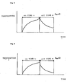
Fig. 3 is an explanatory diagram showing temperature changes when, in the spin valve element in an embodiment of the invention, Don > D; -
Fig. 4 is an explanatory diagram showing temperature changes when, in the spin valve element in an embodiment of the invention, Don < D; -
Fig. 5 is an explanatory diagram showing a driving method for the spin valve element of an embodiment of the invention; -
Fig. 6 is an explanatory diagram showing an example of a spin valve element driving circuit in an embodiment of the invention; -
Fig. 7 is a cross-sectional view showing the basic constituent portions of a spin valve element utilizing TMR; -
Fig. 8 is a cross-sectional view showing the basic constituent portions of a spin valve element utilizing GMR, and is a cross-sectional view showing the structure of the spin valve element of an embodiment of the invention; and -
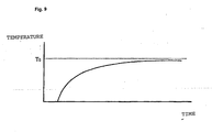
Fig. 9 is an explanatory diagram showing a spin valve element driving method of the prior art. -
- 10
- Spin valve element
- 11
- Insulating member
- 12
- Insulating layer
- 13
- Substrate
- 14
- Heat diffusion portion
- Below, embodiments of the invention are explained referring to the drawings.
A major technical point of this invention is the discovery that, by adopting an operation mode in which heat generation and cooling are repeated by modulating the driving current, the heat diffusion distance of the element is made equal to or greater than a constant value, which is effective for suppressing temperature increases. -
Fig. 1 shows the configuration of aspin valve element 10 which is one embodiment of the invention. Thespin valve element 10 comprises the insulatingmember 11 which is a heat-generating member, aheat diffusion portion 14, an insulatinglayer 12, and asubstrate 13. Theheat diffusion portion 14 is a portion having the function of temporarily holding heat generated by the spin valve element through its own heat capacity, and simultaneously can be used as an electrode to supply current to thespin valve element 10. InFig. 1 , electrodes to supply current to the spin valve element are not shown. The insulatinglayer 12 is a portion which, when considering a system in which heat is generated and enters and exits, effectively functions as a thermal barrier having relatively low thermal conductivity, and can for example be formed by an electrically insulating layer, or in a separate embodiment, can be formed by providing a gap with thesubstrate 13 by means of a supporting member, configured with the air layer of the gap provided at a similar position. When the insulatinglayer 12 is an electrically insulating layer, the insulatinglayer 12 can be formed from inorganic material, plastic, or similar. Even in such cases, compared with the spin valve layers, primarily comprising metal thin films, this portion has a low thermal conductivity. - In general the
substrate 13 is assumed to be a member which can be regarded as effectively at a constant temperature; for example, a substrate which functions as a heat sink can be used. As another example, a cooling water receptacle used for heat dissipation can also be used; in any of these cases, the following discussion applies. In particular, in the following examination, an inorganic material having electrically insulating functions is assumed as the insulatinglayer 12, and a silicon substrate is assumed as thesubstrate 13. These are presented as examples in explaining the advantageous results of the invention, but in no way limit the content of the invention. - Below, the explanation of temperature changes of an element is divided into two stages, which are (A) the temperature increase in the
spin valve element 11 and theheat diffusion portion 14 during the on-time, and (B) heat conduction via the electrically insulatinglayer 12 during repetition of the on-off cycle. - First, the temperature increase in the
spin valve element 11 and theheat diffusion portion 14 during the on-time of (A) is explained. From the configuration ofFig. 1 , only heat conduction in the film thickness direction is considered. Here, the coordinate in the film thickness direction is taken to be x. Heat diffusion in directions parallel to the film plane are in essence not considered, so that the same results can be applied to cases in which elements are arranged in these directions. In this case, the change with time in the temperature distribution is expressed by the following equation.
spin valve element 11 and theheat diffusion portion 14, ρ is the density (kg/m3) of thespin valve element 11 and theheat diffusion portion 14, T(t,x) is the temperature (K) as a function of time t and position x, k is the thermal conductivity (W/mK) of the spin valve element and theheat diffusion portion 14, and Q is the amount of heat generated (W). Here, C, ρ and k are all normally defined as functions of position x; here, however, they are used as values for thespin valve element 11 andheat diffusion portion 14. In effect, the volume of thespin valve element 11 is small compared with that of theheat diffusion portion 14, so that in the following analysis, thespin valve element 11 is assumed in the analysis as a part of theheat diffusion portion 14, having the constant values of C, ρ and k being same as those for the heat diffusion portion14 - Solutions to the above equation will differ with the initial conditions and boundary conditions; from a dimensional analysis of equation (3), the heat diffusion distance Don in the
heat diffusion layer 14 of heat generated by thespin valve element 11 is expressed as a function of the on-time ton as follows.
heat diffusion layer 14. When the Don of the above equation is equal to the thickness D of theheat diffusion layer 14, thermal diffusion proceeds up to Don, and within this range the average temperature Tm rises in proportion to the 0.5 power (square root) of the time, as indicated by the following equation. This behavior is shown inFig. 2 .
heat diffusion layer 14. If the cross-sectional area of theheat diffusion layer 14 is greater than the cross-sectional area of the spin valve element, then the heat conduction area is effectively greater than the heat generation area, and so acts favorably for temperature suppression. - On the other hand, when ton is large and Don is larger than D, heat diffusion is blocked by the insulating
layer 12 with low thermal conductivity, and so the average temperature rises rapidly in proportion to the on-time ton, as in the equation below. This behavior is shown inFig. 3 .
Fig. 4 . - In this way, for suppressing the average temperature of the
spin valve element 11 andheat diffusion layer 14 defined in equations (5) and (6), it is effective to select the on-time, or decide on an element structure, such that Don < D. That is, from (αton)0.5 < D, it is desirable that ton < D2/α. - Next, the heat conduction stage via the insulating
layer 12 in repetition of the on-off cycle in (B) is explained. In the case of the configuration ofFig. 1 , the average temperature T(t) of thespin valve element 11 andheat diffusion layer 14 is expressed as follows.
Here V is the total volume (m3) of thespin valve element 11 and theheat diffusion layer 14, and L is the thickness (m) of the insulatinglayer 12. A solution to equation (7) is given below.


- First, for comparison, a case in which the current is not on-off modulated is considered; the average temperature of the
spin valve element 11 and theheat diffusion layer 14 conforms to equation (2), and as shown inFig. 9 increases with time, asymptotically approaching To (= QL/kS). On the other hand, when the current is modulated with an on-time u (= ton) and off-time v, the temperature changes as shown inFig. 5 . That is, if the temperature at the end of the (n-1)th cycle is Tn-1,b, the temperature at the end of the on-time u of the (n-1)th cycle is Tn,a, the off-time following this is v, and the temperature at the end is Tn,b, then


- In general, when Xn = AXn-1+B, Xn = An+B(1-An)/(1-A), and moreover, when A < 1, as n→∞, Xn→B/(1-A), so that at this time


- In general, the microwave oscillation frequency of a spin valve element is in the range from 1 to 100 GHz, and in order to effectively receive the electromagnetic signals, it is desirable that the on-time in the on-off cycle to suppress overheating be larger than from 0.01 to 1 ns; hence the on-off cycle frequency must be lower than 100 GHz, and preferably should be lower than 1 GHz.
- Conversely, if the thermal diffusivity α of the heat diffusion portion provided in the spin valve element and the thickness D of the heat diffusion portion satisfy the following relation, which is equivalent to an on-off cycle time ratio of 1:1 and 1 GHz, then the above frequencies can be accommodated.

- As the materials forming a spin valve element employing a driving method of this invention, silicon substrate or glass substrate can be used as the
substrate 5, and copper substrate which is highly functional as a heat sink can also be used; where necessary, water cooling or another method can be used for cooling. As the electrode layers 21, 29, 31, Ta, Pt, Cu, Au, Ag, Al, and Mo; as theantiferromagnetic layer 22, IrMn and PtMn; as the ferromagnetic layer 23 (fixed layer), Co, CoFe, CoFeB; as the insulatinglayer 24, MgO and an Al oxide; as thenonmagnetic layer 51, Cu; as the ferromagnetic layer 25 (free layer), Co, CoFe, CoFeB, and NiFe; and as thecapping layer 27, Cu and Pd, are representative examples, but materials are not limited to these. Frequently, the material properties of the ferromagnetic layer 23 (fixed layer) and the ferromagnetic layer 25 (free layer) are made the same, and the film thickness of the former is made greater than the film thickness of the latter, so that a difference in coercive forces is provided, and spin valve functions are achieved. After layering these layers, it is effective to perform magnetic field annealing in order to adjust the crystallinity of the layers and the magnetic anisotropy of the fixed layer. As necessary, the ferromagnetic layer 23 (fixed layer) and ferromagnetic layer 25 (free layer) can for example be made CoFeB/Ru/CoFeB or other antiferromagnetic coupled films. Here, materials indicated using a slash (/) are multilayer films in which layers of the materials are layered in that order. - As the material of the
heat diffusion portion 14, it is preferable that a material with high thermal diffusivity be employed, and Cu, Au, Ag, Al, Mo, or other metal materials are appropriate. - In order to more effectively suppress temperature increases through on-off modulation, it is effective to raise the thermal diffusivity of the insulating
layer 12 to the extent possible. To this end, alumina and aluminum nitride, having high breakdown voltages and heat resistance and with comparatively high thermal diffusivities, are appropriate as the material of the insulatinglayer 12. - Further, a driving method of this invention can be similarly applied to an integrated element in which the above spin valve elements are connected in series or in parallel. As the means of integration, a porous insulating layer obtained, for example, from anodic oxidation of an aluminum film, or resin self-organization, or nanoimprinting technology, is used; in the minute holes thereof are formed the electrodes of spin valve elements, or the insulating layers of spin valve elements, or the nonmagnetic layers and a portion of the ferromagnetic layers, or all of these. By utilizing these porous insulating layers, minute holes with uniform shapes can be formed by an inexpensive process. In particular, if nanoimprinting is used, minute holes can be formed having a high aspect ratio (the ratio of hole depth to hole diameter), which is appropriate for forming layered structures with numerous layers. That is, in general spin valve elements, the magnetic film shape is often made elliptical with the aim of controlling the direction of the in-plane anisotropy of the magnetic film; such shapes can also be formed easily. On the other hand, in anodic oxidation treatment of aluminum film the minute hole shape is circular, and it is difficult to control the direction of the magnetic film in-plane anisotropy, so that in essence it is advantageous to employ a perpendicular magnetization design, with alignment of the crystal anisotropy in a direction perpendicular to the film plane. As the means of crystal anisotropy alignment, generally a Ru underlayer, or a vertical columnar structure, are employed. In resin self-organization also, the minute hole shape is circular, and it is advantageous to employ a perpendicular magnetization design in which the crystal anisotropy is aligned in a direction perpendicular to the film plane. In resin self-organization, minute holes are obtained with an aspect ratio higher than that for nanoimprinting techniques, making this method appropriate for obtaining layered structures of many layers.
- An electric circuit to realize a driving method of this invention can easily be fabricated by using a transistor Tr to control the driving current to drive the
spin valve element 10, for example as shown inFig. 6 . - In this way, driving means can be provided in which local overheating of the spin valve element due to Joule heat is suppressed, and the spin valve element is driven with stability.
- First, a TMR type spin valve element was manufactured by the following procedure. That is, on a
silicon substrate 5 with an oxide film ofthickness 10 nm, a Cu (340 nm) thin film was formed as a diffusion layer/electrode layer 21. Then, Co70Fe30 (20 nm) as theferromagnetic layer 23, MgO (0.6 nm) as the insulatinglayer 24, Co40Fe40B20 (2 nm) as theferromagnetic layer 25, and Cu (2 nm) as thecapping layer 26, were layered in order. Further, a negative resist was applied, and electron beam irradiation was used to perform patterning, after which ion milling was used to form fifty spin valve elements with an elliptical (100 nm × 50 nm) column shape. The spacing between elements, taken to be the distance between centers, was 250 nm. A CVD method was used to form an SiO2 film, after which the resist on the spin valve elements was removed by lift-off, and after forming an upper electrode, annealing was performed at 350°C in a magnetic field of approximately 4 kOe. The electrical resistance of the elements was approximately 2.5 kΩ per element, and by connecting these 50 elements in parallel, a total impedance of approximately 51 Ω could be obtained. In the parentheses following the different materials, the film thickness of the layer is indicated. - Next, a 1 T DC magnetic field was applied to this element in the direction parallel to the magnetic field of the fixed layer, and tests were conducted in which a voltage was applied under the conditions indicated below, so that electrons flowed from the free layer to the fixed layer. That is, on-off voltages of DC 1 V/0 V were applied such that the respective time widths were 1 nsec and 1 nsec, and the temperature reached and the microwave oscillation characteristics were measured. For comparison, measurements were also performed during continuous application of the on voltage.
- After cleaning the surface of a
silicon substrate 5 with hydrofluoric acid and removing the oxide film, sputtering was performed to form an alumina thin film 50 nm as the insulatinglayer 12; otherwise, the spin valve element of Practical Example 2 was formed similarly to that of Practical Example 1 for use as the sample of Practical Example 2, and conduction tests were conducted under conditions similar to those of Practical Example 1. - As the diffusion layer/electrode layer 21 a Cu thin film of thickness 340 nm was used, as the insulating
layer 12 an alumina thin film ofthickness 30 nm was used, and as the insulatinglayer 24 an MgO film of thickness 1.5 nm was used; 2000 elements were formed, with the spacing between elements, taken to be the distance between centers, at 450 nm, and the 2000 elements were connected in parallel; otherwise, manufacturing was similar to that of Practical Example 1, to obtain the sample of Practical Example 3. The electrical resistance of the elements was approximately 102 kΩ per element, and by connecting the 2000 elements in parallel, the total impedance could be made approximately 51 Ω. A 1 T DC magnetic field was applied to this element in the direction parallel to the magnetic field of the fixed layer, and tests were conducted in which a voltage was applied under the conditions indicated below, so that electrons flowed from the free layer to the fixed layer. That is, on-off voltages of DC 40 V/0 V were applied such that the respective time widths were 1 nsec and 2 nsec, and the temperature reached and the microwave oscillation characteristics were measured. For comparison, measurements were also performed during continuous application of the on voltage. - On a
silicon substrate 5 with an oxide film ofthickness 10 nm was formed a Cu (340 nm) thin film as the diffusion layer/electrode layer 21. Then, Ru (5 nm)/Co70Fe30 (20 nm) as theferromagnetic layer 23, a Cu layer (1.5 nm) as thenonmagnetic layer 51, NiFe (4.5 nm) as theferromagnetic layer 25, Cu (2 nm) as thecapping layer 26, and Pt (10 nm) as the intermediate electrode layer 29, were layered in order, to obtain one spin valve layer. By further repeating this process, a total of eleven spin valve layers were layered. Then, a procedure similar to that of Practical Example 1 was used to form five spin valve elements with an elliptical (100 nm × 50 nm) columnar shape. The spacing between elements, taken to be the distance between centers, was 450 nm. After layering Cu (30 nm) as theelectrode layer 27, annealing was performed at 250°C in a magnetic field of approximately 4 kOe, to obtain a sample of Practical Example 4. The electrical resistance of a spin valve layer 20 with this configuration was 23 Ω per layer, and the resistance was approximately 250 Ω for eleven layers connected in series; by connecting these five in parallel, the overall electrical resistance was approximately 50 Ω. A 1 T DC magnetic field was applied to this element in the direction parallel to the magnetic field of the fixed layer, and tests were conducted in which a voltage was applied under the conditions indicated below, so that electrons flowed from the free layer to the fixed layer. That is, on-off voltages of DC 2.5 V/0 V were applied such that the respective time widths were 1 nsec and 1 nsec, and the temperature reached and the microwave oscillation characteristics were measured. For comparison, measurements were also performed during continuous application of the on voltage. - Other than the fact that the thickness of the Cu thin film used as the diffusion layer/
electrode layer 21 was 30 nm, the sample of Comparison Example 1 was formed similarly to that of Practical Example 1, and measurements similar to those of Practical Example 1 were conducted. - Other than the fact that the thickness of the Cu thin film used as the diffusion layer/
electrode layer 21 was 30 nm, the sample of Comparison Example 2 was formed similarly to that of Practical Example 3, and measurements similar to those of Practical Example 3 were conducted. - Calculated results and measured results for Practical Examples 1 through 4 and for Comparison Examples 1 and 2 appear in Table 1.
Table 1 Units Practical Example 1 Practical Example 2 Practical Example 3 Practical Example 4 Comparison Example 1 Comparison Example 2 Calculated on-off modulation equilibrium temperature K 126 49 318 12 189 599 Measured on-off modulation equilibrium temperature K 120 41 309 10 172 597 Microwave output during on-off modulation W 2.0E-05 2.4E-06 3.8E-04 8.3E-09 8.0E-07 < 1.0e-10 Calculated continuous-on equilibrium temperature K 238 83 600 24 238 600 Measured continuous-on equilibrium temperature K 229 67 587 23 225 602 Microwave output during continuous-on W 9.0E-06 1.7E-05 < 1.0e-10 7.2E-09 6.7E-07 < 1.0e-10 - Thus through this invention it is possible to provide means for stable driving of a spin valve element, with local overheating of the spin valve element due to Joule heat suppressed. Embodiments of the invention have been described, but the invention is not limited to the embodiments described, and various modifications, alterations, and combinations are possible based on the technical concepts of the invention.
Claims (7)
- A method of driving a spin valve element having an intermediate layer which is an insulating member or a nonmagnetic member and a pair of ferromagnetic layers sandwiching the intermediate layer, with a driving current being passed through the spin valve element thereby obtaining an oscillation signal,
the method comprising a step of performing amplitude modulation of the driving current by a frequency lower than the oscillation frequency of the oscillation signal. - The method of driving a spin valve element according to Claim 1, wherein the amplitude modulation is binary ON-OFF modulation comprising a conducting state and a shutoff state, and in the shutoff state the driving current passed through the spin valve element is zero.
- The method of driving a spin valve element according to Claim 1 or Claim 2, wherein the spin valve element further comprises a heat diffusion portion, the heat diffusion portion is provided in contact with a face which is a face of either of the ferromagnetic layers and which is not in contact with the intermediate layer, and wherein the interval ton of the conducting state of the ON-OFF modulation is an interval satisfying the relation

where α is a thermal diffusivity of the heat diffusion portion and D is a thickness of the heat diffusion portion. - The method of driving a spin valve element according to Claim 1 or Claim 2, wherein the oscillation frequency is in a range from 1 GHz to 100 GHz, and the ON-OFF modulation frequency is less than 1 GHz.
- The method of driving a spin valve element according to Claim 3, wherein the oscillation frequency is in a range from 1 GHz to 100 GHz, and the ON-OFF modulation frequency is less than 1 GHz.
- A spin valve element, comprising: an intermediate layer which is an insulating member or a nonmagnetic member; a pair of ferromagnetic layers sandwiching the intermediate layer; and a heat diffusion portion, wherein
the heat diffusion portion is provided in contact with a face which is a face of either of the ferromagnetic layers and which is not in contact with the intermediate layer, and wherein the thickness D of the heat diffusion portion satisfies the relation
where α is a thermal diffusivity of the heat diffusion portion. - The spin valve element according to Claim 6, wherein the heat diffusion portion is used as an electrode which supplies the driving current to the spin valve element.
Applications Claiming Priority (2)
| Application Number | Priority Date | Filing Date | Title |
|---|---|---|---|
| JP2007278545 | 2007-10-26 | ||
| PCT/JP2008/065423 WO2009054183A1 (en) | 2007-10-26 | 2008-08-28 | Spin valve element, and its driving method |
Publications (2)
| Publication Number | Publication Date |
|---|---|
| EP2214313A1 true EP2214313A1 (en) | 2010-08-04 |
| EP2214313A4 EP2214313A4 (en) | 2012-03-07 |
Family
ID=40579290
Family Applications (1)
| Application Number | Title | Priority Date | Filing Date |
|---|---|---|---|
| EP08842281A Withdrawn EP2214313A4 (en) | 2007-10-26 | 2008-08-28 | SPIN VALVE ELEMENT AND METHOD FOR MANUFACTURING THE SAME |
Country Status (5)
| Country | Link |
|---|---|
| US (1) | US8411395B2 (en) |
| EP (1) | EP2214313A4 (en) |
| JP (1) | JPWO2009054183A1 (en) |
| KR (1) | KR101456950B1 (en) |
| WO (1) | WO2009054183A1 (en) |
Families Citing this family (5)
| Publication number | Priority date | Publication date | Assignee | Title |
|---|---|---|---|---|
| US8581672B2 (en) * | 2010-05-14 | 2013-11-12 | Nokia Corporation | Frequency synthesis |
| FR2974468B1 (en) | 2011-04-20 | 2013-05-31 | Commissariat Energie Atomique | DEMODULATOR OF AN ELECTRICAL SIGNAL FREQUENCY MODULE |
| US8542456B2 (en) * | 2011-08-25 | 2013-09-24 | Tdk Corporation | Magnetic head having a contact sensor |
| US8619394B1 (en) * | 2012-11-29 | 2013-12-31 | HGST Netherlands B.V. | Magnetic tunnel junction with barrier cooling for magnetic read head |
| KR102088313B1 (en) * | 2017-11-16 | 2020-03-13 | 성균관대학교 산학협력단 | Controllable magnetic properties halide electride |
Family Cites Families (3)
| Publication number | Priority date | Publication date | Assignee | Title |
|---|---|---|---|---|
| DE69804768T2 (en) * | 1997-01-31 | 2002-09-12 | Thomson Consumer Electronics, Inc. | REMOTE CONTROL DEVICE AND METHOD FOR THIS |
| JP4677589B2 (en) * | 2005-03-18 | 2011-04-27 | 独立行政法人科学技術振興機構 | Transmission circuit integrated microwave generation element and microwave detection method, microwave detection circuit, microwave detection element, and transmission circuit integrated microwave detection element |
| US7678475B2 (en) * | 2006-05-05 | 2010-03-16 | Slavin Andrei N | Spin-torque devices |
-
2008
- 2008-08-28 US US12/739,740 patent/US8411395B2/en not_active Expired - Fee Related
- 2008-08-28 KR KR1020107008724A patent/KR101456950B1/en not_active Expired - Fee Related
- 2008-08-28 WO PCT/JP2008/065423 patent/WO2009054183A1/en not_active Ceased
- 2008-08-28 JP JP2009537991A patent/JPWO2009054183A1/en active Pending
- 2008-08-28 EP EP08842281A patent/EP2214313A4/en not_active Withdrawn
Also Published As
| Publication number | Publication date |
|---|---|
| KR101456950B1 (en) | 2014-10-31 |
| KR20100084633A (en) | 2010-07-27 |
| US20100296203A1 (en) | 2010-11-25 |
| EP2214313A4 (en) | 2012-03-07 |
| US8411395B2 (en) | 2013-04-02 |
| JPWO2009054183A1 (en) | 2011-03-03 |
| WO2009054183A1 (en) | 2009-04-30 |
Similar Documents
| Publication | Publication Date | Title |
|---|---|---|
| Demidov et al. | Spin–orbit-torque magnonics | |
| Zeng et al. | High-power coherent microwave emission from magnetic tunnel junction nano-oscillators with perpendicular anisotropy | |
| Maehara et al. | Large emission power over 2 µW with high Q factor obtained from nanocontact magnetic-tunnel-junction-based spin torque oscillator | |
| US8564293B2 (en) | Method for changing spin relaxation, method for detecting spin current and spintronics device using spin relaxation | |
| JP2005025831A (en) | High frequency oscillation element, magnetic information recording head, and magnetic storage device | |
| US20120302446A1 (en) | Josephson magnetic switch | |
| US8411395B2 (en) | Spin valve element and method of driving same | |
| JP5278876B2 (en) | Microwave oscillation element and detection element | |
| Boone et al. | Experimental test of an analytical theory of spin-torque-oscillator dynamics | |
| US11533020B2 (en) | Single magnetic-layer microwave oscillator | |
| US20080150643A1 (en) | Microwave Transmission Line Integrated Microwave Generating Element and Microwave Transmission Line Integrated Microwave Detecting Element | |
| Lebrun et al. | Nonlinear behavior and mode coupling in spin-transfer nano-oscillators | |
| Tsou et al. | Thermally robust perpendicular SOT-MTJ memory cells with STT-assisted field-free switching | |
| Han et al. | Large tunneling magnetoresistance in van der Waals magnetic tunnel junctions based on FeCl 2 films with interlayer antiferromagnetic couplings | |
| Huai et al. | Spin-transfer switching current distribution and reduction in magnetic tunneling junction-based structures | |
| Bakker et al. | Thermoelectric detection of ferromagnetic resonance of a nanoscale ferromagnet | |
| Surampalli et al. | Voltage controlled interlayer exchange coupling and magnetic anisotropy effects in perpendicular magnetic heterostructures | |
| Pan et al. | Field-free spin-orbit torque switching of Co/Pd memory layer in CPP-GMR with perpendicularly magnetized SAF pinned layer | |
| Luo et al. | Enhanced spin–orbit torque and field-free switching in Au/TMDs/Ni hybrid structures | |
| Chen et al. | Spatial coexistence of multiple modes in a nanogap spin Hall nano-oscillator with extended Pt/Ni/Fe trilayers | |
| Abreu Araujo et al. | Spin-transfer-torque driven vortex dynamics in electrodeposited nanowire spin-valves | |
| Chen et al. | Controllable excitation of multiple spin wave bullet modes in a spin Hall nano-oscillator based on [Ni/Co]/Pt multilayers | |
| Kent et al. | Magnetization dynamics | |
| CN118475218A (en) | Three-dimensional spin Hall nano oscillator series-parallel array and preparation method thereof | |
| Rathore et al. | Magnon-magnon coupling in an all-oxide insulator garnet Y 3 Fe 5 O 12/Tm 3 Fe 5 O 12 heterostructure |
Legal Events
| Date | Code | Title | Description |
|---|---|---|---|
| PUAI | Public reference made under article 153(3) epc to a published international application that has entered the european phase |
Free format text: ORIGINAL CODE: 0009012 |
|
| 17P | Request for examination filed |
Effective date: 20100312 |
|
| AK | Designated contracting states |
Kind code of ref document: A1 Designated state(s): AT BE BG CH CY CZ DE DK EE ES FI FR GB GR HR HU IE IS IT LI LT LU LV MC MT NL NO PL PT RO SE SI SK TR |
|
| AX | Request for extension of the european patent |
Extension state: AL BA MK RS |
|
| RIN1 | Information on inventor provided before grant (corrected) |
Inventor name: KAWAKAMI, HARUO Inventor name: ADACHI, EIKI Inventor name: OGIMOTO, YASUSHI |
|
| DAX | Request for extension of the european patent (deleted) | ||
| RAP1 | Party data changed (applicant data changed or rights of an application transferred) |
Owner name: FUJI ELECTRIC CO., LTD. |
|
| RIC1 | Information provided on ipc code assigned before grant |
Ipc: H01L 29/82 20060101ALI20120120BHEP Ipc: H03B 15/00 20060101ALI20120120BHEP Ipc: H03K 3/02 20060101AFI20120120BHEP Ipc: H03K 3/45 20060101ALI20120120BHEP Ipc: H01F 10/32 20060101ALI20120120BHEP Ipc: G11C 11/16 20060101ALI20120120BHEP Ipc: H01L 43/08 20060101ALI20120120BHEP Ipc: H01L 43/12 20060101ALI20120120BHEP |
|
| A4 | Supplementary search report drawn up and despatched |
Effective date: 20120203 |
|
| RIC1 | Information provided on ipc code assigned before grant |
Ipc: H01L 43/08 20060101ALI20120127BHEP Ipc: H01L 43/12 20060101ALI20120127BHEP Ipc: H03K 3/02 20060101AFI20120127BHEP Ipc: H03K 3/45 20060101ALI20120127BHEP Ipc: H01L 29/82 20060101ALI20120127BHEP Ipc: G11C 11/16 20060101ALI20120127BHEP Ipc: H01F 10/32 20060101ALI20120127BHEP Ipc: H03B 15/00 20060101ALI20120127BHEP |
|
| RAP1 | Party data changed (applicant data changed or rights of an application transferred) |
Owner name: III HOLDINGS 3 LLC |
|
| RAP1 | Party data changed (applicant data changed or rights of an application transferred) |
Owner name: III HOLDINGS 3, LLC |
|
| 17Q | First examination report despatched |
Effective date: 20171006 |
|
| GRAP | Despatch of communication of intention to grant a patent |
Free format text: ORIGINAL CODE: EPIDOSNIGR1 |
|
| INTG | Intention to grant announced |
Effective date: 20180306 |
|
| STAA | Information on the status of an ep patent application or granted ep patent |
Free format text: STATUS: THE APPLICATION IS DEEMED TO BE WITHDRAWN |
|
| 18D | Application deemed to be withdrawn |
Effective date: 20180717 |