EP2211369A1 - Arrangement for working substrates by means of plasma - Google Patents
Arrangement for working substrates by means of plasma Download PDFInfo
- Publication number
- EP2211369A1 EP2211369A1 EP09151239A EP09151239A EP2211369A1 EP 2211369 A1 EP2211369 A1 EP 2211369A1 EP 09151239 A EP09151239 A EP 09151239A EP 09151239 A EP09151239 A EP 09151239A EP 2211369 A1 EP2211369 A1 EP 2211369A1
- Authority
- EP
- European Patent Office
- Prior art keywords
- electrodes
- arrangement
- plasma
- gas
- substrate
- Prior art date
- Legal status (The legal status is an assumption and is not a legal conclusion. Google has not performed a legal analysis and makes no representation as to the accuracy of the status listed.)
- Withdrawn
Links
- 239000000758 substrate Substances 0.000 title claims abstract description 25
- VYPSYNLAJGMNEJ-UHFFFAOYSA-N silicon dioxide Inorganic materials O=[Si]=O VYPSYNLAJGMNEJ-UHFFFAOYSA-N 0.000 claims description 27
- 238000000034 method Methods 0.000 claims description 21
- 239000010453 quartz Substances 0.000 claims description 18
- 239000012212 insulator Substances 0.000 claims description 13
- 230000008569 process Effects 0.000 claims description 13
- 239000002826 coolant Substances 0.000 claims 2
- 238000001816 cooling Methods 0.000 claims 2
- 238000000623 plasma-assisted chemical vapour deposition Methods 0.000 abstract description 16
- 239000007789 gas Substances 0.000 description 49
- 210000002381 plasma Anatomy 0.000 description 37
- 239000000498 cooling water Substances 0.000 description 13
- 238000010586 diagram Methods 0.000 description 6
- 238000006243 chemical reaction Methods 0.000 description 5
- 238000010438 heat treatment Methods 0.000 description 5
- 230000008901 benefit Effects 0.000 description 4
- 238000000151 deposition Methods 0.000 description 4
- 230000008021 deposition Effects 0.000 description 4
- 230000000694 effects Effects 0.000 description 4
- UQEAIHBTYFGYIE-UHFFFAOYSA-N hexamethyldisiloxane Chemical compound C[Si](C)(C)O[Si](C)(C)C UQEAIHBTYFGYIE-UHFFFAOYSA-N 0.000 description 4
- CURLTUGMZLYLDI-UHFFFAOYSA-N Carbon dioxide Chemical compound O=C=O CURLTUGMZLYLDI-UHFFFAOYSA-N 0.000 description 3
- 229910021417 amorphous silicon Inorganic materials 0.000 description 3
- 230000015572 biosynthetic process Effects 0.000 description 3
- 210000004027 cell Anatomy 0.000 description 3
- 229910052681 coesite Inorganic materials 0.000 description 3
- 229910052906 cristobalite Inorganic materials 0.000 description 3
- 238000009434 installation Methods 0.000 description 3
- 238000004519 manufacturing process Methods 0.000 description 3
- 239000000377 silicon dioxide Substances 0.000 description 3
- 229910052682 stishovite Inorganic materials 0.000 description 3
- 229910052905 tridymite Inorganic materials 0.000 description 3
- BLRPTPMANUNPDV-UHFFFAOYSA-N Silane Chemical compound [SiH4] BLRPTPMANUNPDV-UHFFFAOYSA-N 0.000 description 2
- 229910002092 carbon dioxide Inorganic materials 0.000 description 2
- 238000005229 chemical vapour deposition Methods 0.000 description 2
- 239000004020 conductor Substances 0.000 description 2
- 230000005684 electric field Effects 0.000 description 2
- 150000002500 ions Chemical class 0.000 description 2
- 239000000463 material Substances 0.000 description 2
- 239000000203 mixture Substances 0.000 description 2
- 230000007704 transition Effects 0.000 description 2
- XLYOFNOQVPJJNP-UHFFFAOYSA-N water Chemical compound O XLYOFNOQVPJJNP-UHFFFAOYSA-N 0.000 description 2
- 229910001868 water Inorganic materials 0.000 description 2
- QVGXLLKOCUKJST-UHFFFAOYSA-N atomic oxygen Chemical compound [O] QVGXLLKOCUKJST-UHFFFAOYSA-N 0.000 description 1
- 239000006227 byproduct Substances 0.000 description 1
- 239000003990 capacitor Substances 0.000 description 1
- 239000001569 carbon dioxide Substances 0.000 description 1
- 239000000919 ceramic Substances 0.000 description 1
- 238000005234 chemical deposition Methods 0.000 description 1
- 238000004140 cleaning Methods 0.000 description 1
- 239000011248 coating agent Substances 0.000 description 1
- 238000000576 coating method Methods 0.000 description 1
- 238000010276 construction Methods 0.000 description 1
- 229910021419 crystalline silicon Inorganic materials 0.000 description 1
- 230000003247 decreasing effect Effects 0.000 description 1
- 230000007547 defect Effects 0.000 description 1
- 238000009826 distribution Methods 0.000 description 1
- 238000005530 etching Methods 0.000 description 1
- 230000005284 excitation Effects 0.000 description 1
- 238000010574 gas phase reaction Methods 0.000 description 1
- 230000006872 improvement Effects 0.000 description 1
- 239000011261 inert gas Substances 0.000 description 1
- 238000009413 insulation Methods 0.000 description 1
- 238000010849 ion bombardment Methods 0.000 description 1
- 238000003913 materials processing Methods 0.000 description 1
- 230000004048 modification Effects 0.000 description 1
- 238000012986 modification Methods 0.000 description 1
- 230000003287 optical effect Effects 0.000 description 1
- 229910052760 oxygen Inorganic materials 0.000 description 1
- 239000001301 oxygen Substances 0.000 description 1
- 239000002245 particle Substances 0.000 description 1
- 230000005855 radiation Effects 0.000 description 1
- 239000012495 reaction gas Substances 0.000 description 1
- 230000009467 reduction Effects 0.000 description 1
- 230000001105 regulatory effect Effects 0.000 description 1
- 239000004065 semiconductor Substances 0.000 description 1
- 150000004756 silanes Chemical class 0.000 description 1
- 125000006850 spacer group Chemical group 0.000 description 1
- 238000004544 sputter deposition Methods 0.000 description 1
- 239000000126 substance Substances 0.000 description 1
- 238000006467 substitution reaction Methods 0.000 description 1
- 238000006557 surface reaction Methods 0.000 description 1
- 238000007725 thermal activation Methods 0.000 description 1
Images


Classifications
-
- H—ELECTRICITY
- H01—ELECTRIC ELEMENTS
- H01J—ELECTRIC DISCHARGE TUBES OR DISCHARGE LAMPS
- H01J37/00—Discharge tubes with provision for introducing objects or material to be exposed to the discharge, e.g. for the purpose of examination or processing thereof
- H01J37/32—Gas-filled discharge tubes
- H01J37/32431—Constructional details of the reactor
- H01J37/3244—Gas supply means
- H01J37/32449—Gas control, e.g. control of the gas flow
-
- H—ELECTRICITY
- H01—ELECTRIC ELEMENTS
- H01J—ELECTRIC DISCHARGE TUBES OR DISCHARGE LAMPS
- H01J37/00—Discharge tubes with provision for introducing objects or material to be exposed to the discharge, e.g. for the purpose of examination or processing thereof
- H01J37/32—Gas-filled discharge tubes
- H01J37/32431—Constructional details of the reactor
- H01J37/3244—Gas supply means
Definitions
- the invention relates to an arrangement according to the preamble of patent claim 1.
- the plasma can burn directly at the substrate to be coated or in a separate chamber. In the first case, the method is referred to as direct plasma method, in the second case as remote plasma method.
- a strong electric field is applied, through which a plasma is ignited.
- the plasma causes the opening of the bonds of a reaction gas, for example SiH 4 , and decomposes it into radicals which are deposited on the substrate and cause here the chemical deposition reaction.
- a higher deposition rate at lower deposition temperatures, for example 200 - 300 °C, than with the CVD method can thereby be attained.
- the plasma is so disposed that it has no direct contact with the substrate. It is hereby possible to excite selectively individual components of a process gas mixture. The probability of damage of the substrate surface through the plasma is, moreover, low. Of disadvantage are the possible loss of radicals on the path between the remote plasma and the substrate; in addition, gas phase reactions can already occur before the reactive gas molecules reach the substrate surface.
- PECVD plasmas can also be generated inductively or capacitively through the irradiation of alternating electric fields, making electrodes superfluous.
- the PECVD method is applied in the semiconductor production and also in the production of solar cells or capacitors.
- Gases to be considered for use in plasma processes are, for example N 2 O, NH 3 , N 2 , SiH 4 or other silanes.
- HMDSO C 6 H 18 O 2 Si 2
- a mixture of HMDSO, oxygen and perhaps an inert gas as excitation gas is introduced into a reaction chamber.
- the plasma subsequently breaks down the HMDSO molecules into their components, and substantially H 2 O, CO 2 and SiO 2 , however also byproducts, are produced in the reaction. Only the SiO 2 fraction contributes to the formation of the layer.
- the volatile or gaseous molecules such as for example water and carbon dioxide, are pumped off.
- An arrangement for the generation of plasma which includes two first electrodes connected to a voltage source and two grounded electrodes, with the first of the two grounded electrodes located in front of the first of the other electrodes and the first of the other electrodes disposed in front of the second grounded electrode ( EP 1 475 824 A1 ).
- a first passage between a central first electrode permits the inlet of raw gas (first gas) which serves for the formation of a film on a substrate.
- a plasma discharge space of a second passage is provided between the first and second electrode, and specifically on both sides, whereby the excitable gas (second gas) can pass through.
- the raw gas can subsequently form a film, while the excitable gas itself is only excited and not utilized for the formation of a film.
- An arrangement for the deposition of a substance out of the gas phase onto a substrate is furthermore disclosed ( JP 2002-158219 ).
- This arrangement comprises several electrodes and between the electrodes two gas inlet channels and two gas outlet channels are provided.
- a system for the working of substrates by means of plasma is furthermore known, with which the occurrence of flash-overs between an electrode in a dielectric is to be prevented (EP 1 796 442 A1 ).
- This system includes two working units, between which a gap is formed through which process gas is conducted.
- a plasma working arrangement is also known with which a substrate can be worked effectively ( JP 2005-026062 ).
- a substrate is transported parallel to three successively disposed electrodes. Between the electrodes gas supply means and gas drainage means are provided. Two of the electrodes are connected to a common voltage source.
- the invention addresses the problem of providing a cost-effective arrangement for a PECVD working method.
- the invention relates thus to an arrangement for the working of substrates by means of plasma (PECVD), wherein at least two electrodes are provided, which are disposed in a common plane and are spaced apart from one another. Between each of the electrodes are provided interspaces which serve as gas inlets or gas outlets.
- PECVD plasma
- the advantage attained with the invention comprises in particular that an arrangement with several electrodes is provided, which has a small overall size since it is not necessary to provide each electrode with its own plasma source.
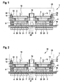
- Fig. 1 shows a plasma chamber 1 in cross section, which includes two electrodes 2, 3 having the form of a T in cross section and being disposed in a common plane. On the underside of these electrodes 2, 3 are provided quartz plates 4, 5 supported by bearing supports 6, 7 and 8, 9, respectively. Electrical connections 12, 13 lead to voltage sources not shown, which can be AC voltage sources with a frequency greater than 1 kHz. Preferably both electrodes 2, 3 are connected to a common voltage source. At the particular opposite ends of the electrodes 2, 3 gas inlets 14, 15 are provided, while between the opposing ends of electrodes 2, 3 a gas outlet 16 is provided.
- the gas inflow direction is herein indicated by arrows 35, 36, while the gas outflow direction is symbolized by arrows 24, 25.
- a counterelectrode 17 Below the quartz plates 4, 5 is depicted a counterelectrode 17. Above the counterelectrode 17 is located a substrate 26 which is transported in the direction of arrow 18. Between the quartz plates 4, 5 and the substrate 26 can be seen plasma clouds 19, 20, and beneath the counterelectrode 17 optionally heating elements 21, 22 are provided, which ensure a temperature-controlled counterelectrode 17.
- a matched housing 23 encompassing the two electrodes 2, 3 on the atmospheric side is indicated by means of dashed lines. Outside and underneath this housing 23 atmospheric pressure obtains, while beneath the quartz plates 4, 5 and the heating elements 21, 22 vacuum obtains. The housing 23 serves for high-frequency radiation shielding and as a contact guard against energized structural parts.
- connection 12, 13 can be connected to a separate voltage source; however, it is also feasible to connect both connections 12, 13 to a single voltage source.
- Fig. 2 shows an arrangement 30 which largely conforms to arrangement 1.
- the gas inlets and gas outlets are interchanged in the arrangement of Fig 2 .
- the reference number 16 now indicates the gas inlet, with arrows 31, 32 symbolizing the direction of gas flow, while the gas inlets 14, 15 according to Fig. 1 now serve as the gas outlets.
- Arrows 33, 34 indicate herein the direction of gas flows.
- the quartz plates 4, 5 are of advantage in terms of processing technique particularly if higher current and power densities are utilized, for example in a ⁇ c-Si process.
- quartz plates 4, 5 are of advantage.
- an "alpha regime” i.e. at low voltage or power density, such as are characteristic of a-Si
- the ionization is mainly localized in the plasma, such that the role of the quartz plates can be neglected.
- plates of another electrically non-conducting material for example plates of ceramic, can also be utilized.
- the transition from good electrical-optical a-Si:H quality which is referred to as alpha-gamma transition, is in general observed at ⁇ 15 eV, which in a PECVD installation can correspond to an electrode voltage of approximately 200 to 300 Volt.
- the use of quartz plates consequently makes possible a relative increase of the power and therewith of the coating rate.
- the quartz plates moreover, isolate the expensive mechanical structural parts - the electrodes and the insulators - from the process volume proper, i.e. no chemical-thermal reaction takes place between the plasma and these components. Only the quartz-glass sheets are directly exposed to this process. However, if necessary, they can be readily exchanged.
- quartz glass can additionally play out its excellent resistance properties.
- atomic components are knocked out of the source itself, i.e. a sputtering or disintegration process occurs.
- These atomic components are consequently also incorporated in the generated layers on the substrate. If this substrate is an electrically conducting material, this leads, for example in the production of a solar cell active layer, to the result that microscopically small shortcircuits form which, in turn, can have a negative effect on the efficiency of the finished solar cell.
- the quartz plates the major portion of the metallic source surface is covered such that the sputter effect is mainly limited to atomic quartz particles. Since quartz is an insulator, this does not present a problem for most applications.
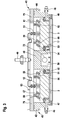
- Fig. 3 shows an enlarged and modified diagram of the PECVD source depicted in Fig. 1 .
- the substrate 26 and the heating elements 21, 22 are here omitted.
- Evident are again the electrodes 2 and 3 as well as the connections 12 and 13, which are here combined on a common electrical connector. Beneath the electrodes 2, 3 is evident the counterelectrode 17.
- a power connector bolt which leads to a, not shown, matching network.
- An adapter flange 41 rests on a source flange 43, which terminates in a VCR threaded connector 45, 46 for a gas pipework. Of this adapter flange 41 only lateral regions 75, 76 are evident.
- a gas supply bar 47, 48 is provided which is provided over its entire length with holes or slits or nozzles, through which process gases are introduced. Through the appropriate distances of these holes with respect to one another and through appropriate cross sections of the holes a mixed gas distribution in the plasma volume is attained. The holes extend into the plane of drawing of Fig. 3 and are therefore not visible.
- the source flange 43 includes a central region 49 as well as two lateral regions 42, 44.
- a gas outlet channel 50 which can be provided at the suction side, for example, with DN40 ISO-KF connectors.
- a connector 73 is evident in Fig. 3 .
- Circumferentially encompassing insulators 51 to 54 represent an electric insulation between the electrodes 2, 3 and the source flange 43.
- the insulators 51 to 54 herein do not encompass the upper portion of the T-shaped electrode 2, 3.
- a cooling water return flow tube 56, 58 implemented as a hose assembly, as well as a cooling water forward flow tube 55, 57, also implemented as a hose assembly.
- a cooling water forward flow tube 59, 61 on a cooling water return flow tube 60, 62.
- the cooling water serves for the temperature control of the electrode bodies.
- Fig. 4 shows the arrangement according to Fig. 1 in a perspective diagram. Evident are here the housing 23 enclosing a voltage source or a matching network, a door 70 to the arrangement 1, the electrodes 2, 3, the gas inlet 14, the gas outlet 16.
- Fig. 5 is depicted once again the source flange 43 shown in Fig. 3 in a view from the atmospheric side.
- the central region 49 of the source flange 43 as well as its two outer regions 42 and 44, wherein all regions are connected with one another via webs 64 to 67.
- Projections 68, 69, 71, 72 are provided at the lower margins of the source flange 43.
- the suction-side connector 73 of gas outlet channel 50 At the lower end of the central region 49 can be seen the suction-side connector 73 of gas outlet channel 50.
- Fig. 6 shows the same source flange 43 as Fig. 4 , however viewed from the vacuum side.
- the gas outlet channel 50 is encompassed by two webs 81, 82.
- two suction-side connectors 73, 87 are visible to which lines connected to a vacuum pump, can be connected.
- a vacuum pump as well as the lines are not shown in Fig. 6 .
- Fig. 7 shows the adapter flange 41 depicted in Fig. 3 in a view from the atmospheric side.
- This adapter flange 41 is also denoted as spacer flange 41.
- the lateral regions 75 and 76 are also denoted as the transverse regions 85, 86 connecting these.
- the size of the plasma volume i.e. the region between electrodes or quartz glass plates and counterelectrode can, inter alia , be varied whereby a direct effect can be exerted onto the plasma density and onto the process.
Landscapes
- Physics & Mathematics (AREA)
- Engineering & Computer Science (AREA)
- Plasma & Fusion (AREA)
- Chemical & Material Sciences (AREA)
- Analytical Chemistry (AREA)
Abstract
Description
- The invention relates to an arrangement according to the preamble of patent claim 1.
- Plasma enhanced chemical vapor deposition (Plasma Enhanced Chemical Vapor Deposition = PECVD) is a special form of chemical vapor deposition = CVD), in which the deposition of thin layers is enhanced through chemical reaction by means of CVD. Instead of the thermal activation in CVD, the surface reaction is regulated or highly modified via the plasma properties (Liebermann and Lichtenberg: Principles of Plasma Discharges and Materials Processing, 2nd Edition, 2005, p. 621 ff.). The plasma can burn directly at the substrate to be coated or in a separate chamber. In the first case, the method is referred to as direct plasma method, in the second case as remote plasma method.
- In the direct plasma method between the substrate and a counterelectrode a strong electric field is applied, through which a plasma is ignited. The plasma causes the opening of the bonds of a reaction gas, for example SiH4, and decomposes it into radicals which are deposited on the substrate and cause here the chemical deposition reaction. A higher deposition rate at lower deposition temperatures, for example 200 - 300 °C, than with the CVD method can thereby be attained.
- In the remote plasma method the plasma is so disposed that it has no direct contact with the substrate. It is hereby possible to excite selectively individual components of a process gas mixture. The probability of damage of the substrate surface through the plasma is, moreover, low. Of disadvantage are the possible loss of radicals on the path between the remote plasma and the substrate; in addition, gas phase reactions can already occur before the reactive gas molecules reach the substrate surface.
- PECVD plasmas can also be generated inductively or capacitively through the irradiation of alternating electric fields, making electrodes superfluous.
- The PECVD method is applied in the semiconductor production and also in the production of solar cells or capacitors. Gases to be considered for use in plasma processes are, for example N2O, NH3, N2, SiH4 or other silanes. If there is the wish to produce, for example SiO2 layers by means of hexamethyldisiloxane = HMDSO = C6H18O2Si2, a mixture of HMDSO, oxygen and perhaps an inert gas as excitation gas is introduced into a reaction chamber. The plasma subsequently breaks down the HMDSO molecules into their components, and substantially H2O, CO2 and SiO2, however also byproducts, are produced in the reaction. Only the SiO2 fraction contributes to the formation of the layer. The volatile or gaseous molecules, such as for example water and carbon dioxide, are pumped off.
- An arrangement for the generation of plasma is already known, which includes two first electrodes connected to a voltage source and two grounded electrodes, with the first of the two grounded electrodes located in front of the first of the other electrodes and the first of the other electrodes disposed in front of the second grounded electrode (
EP 1 475 824 A1 ). A first passage between a central first electrode permits the inlet of raw gas (first gas) which serves for the formation of a film on a substrate. A plasma discharge space of a second passage is provided between the first and second electrode, and specifically on both sides, whereby the excitable gas (second gas) can pass through. The raw gas can subsequently form a film, while the excitable gas itself is only excited and not utilized for the formation of a film. - An arrangement for the deposition of a substance out of the gas phase onto a substrate is furthermore disclosed (
JP 2002-158219 - A system for the working of substrates by means of plasma is furthermore known, with which the occurrence of flash-overs between an electrode in a dielectric is to be prevented (
EP 1 796 442 A1 ). This system includes two working units, between which a gap is formed through which process gas is conducted. - Furthermore is known a PECVD installation with which photovoltaic materials can be applied onto a substrate (
US 2006/0219170 A1 ). This installation includes a cathode with two opposing surfaces, with a system distributing a process gas being integrated in the electrode. - Lastly, a plasma working arrangement is also known with which a substrate can be worked effectively (
JP 2005-026062 - The invention addresses the problem of providing a cost-effective arrangement for a PECVD working method.
- This problem is solved according to the features of claim 1.
- The invention relates thus to an arrangement for the working of substrates by means of plasma (PECVD), wherein at least two electrodes are provided, which are disposed in a common plane and are spaced apart from one another. Between each of the electrodes are provided interspaces which serve as gas inlets or gas outlets.
- The advantage attained with the invention comprises in particular that an arrangement with several electrodes is provided, which has a small overall size since it is not necessary to provide each electrode with its own plasma source.
- Embodiment examples of the invention are shown in the drawing and will be described in further detail in the following. In the drawing depict:
- Fig. 1
- a schematic diagram of a first PECVD source with two electrodes,
- Fig. 2
- a schematic diagram of a second PECVD source with two electrodes,
- Fig. 3
- an enlarged diagram of a PECVD source corresponding to the PECVD source shown in
Fig. 1 , - Fig. 4
- a perspective diagram of parts of the PECVD source according to
Fig. 3 , - Fig. 5
- a source flange viewed from the atmospheric side,
- Fig. 6
- the source flange according to
Fig. 5 , viewed from the vacuum side, - Fig. 7
- an adapter flange.
-
Fig. 1 shows a plasma chamber 1 in cross section, which includes twoelectrodes electrodes quartz plates bearing supports Electrical connections electrodes electrodes gas inlets electrodes 2, 3 agas outlet 16 is provided. The gas inflow direction is herein indicated byarrows arrows - Below the
quartz plates counterelectrode 17. Above thecounterelectrode 17 is located asubstrate 26 which is transported in the direction ofarrow 18. Between thequartz plates substrate 26 can be seenplasma clouds counterelectrode 17 optionallyheating elements counterelectrode 17. A matchedhousing 23 encompassing the twoelectrodes housing 23 atmospheric pressure obtains, while beneath thequartz plates heating elements housing 23 serves for high-frequency radiation shielding and as a contact guard against energized structural parts. - By 10 and 11 are denoted insulators encompassing the T-shaped
electrodes - Although only two electrodes are shown in
Fig. 1 , more than two electrodes can also be provided. Each of theconnections connections -
Fig. 2 shows anarrangement 30 which largely conforms to arrangement 1. However, in contrast to the arrangement ofFig. 1 , the gas inlets and gas outlets are interchanged in the arrangement ofFig 2 . Thereference number 16 now indicates the gas inlet, witharrows gas inlets Fig. 1 now serve as the gas outlets.Arrows - The
quartz plates quartz plates quartz plates - With the aid of
quartz plates -
Fig. 3 shows an enlarged and modified diagram of the PECVD source depicted inFig. 1 . Thesubstrate 26 and theheating elements electrodes connections electrodes counterelectrode 17. - By 40 is denoted a power connector bolt, which leads to a, not shown, matching network. An
adapter flange 41 rests on asource flange 43, which terminates in a VCR threadedconnector adapter flange 41 onlylateral regions gas supply bar Fig. 3 and are therefore not visible. - The source flange 43 includes a
central region 49 as well as twolateral regions gas outlet channel 50 which can be provided at the suction side, for example, with DN40 ISO-KF connectors. Such aconnector 73 is evident inFig. 3 .Circumferentially encompassing insulators 51 to 54 represent an electric insulation between theelectrodes source flange 43. Theinsulators 51 to 54 herein do not encompass the upper portion of the T-shapedelectrode - On the
left electrode 2 is disposed a cooling waterreturn flow tube tube 55, 57, also implemented as a hose assembly. Above thesecond electrode 3 are correspondingly disposed a cooling water forward flowtube return flow tube - Into the
adapter flange 41 lead several securement bolts, of which one is provided with thereference number 63. -
Fig. 4 shows the arrangement according toFig. 1 in a perspective diagram. Evident are here thehousing 23 enclosing a voltage source or a matching network, adoor 70 to the arrangement 1, theelectrodes gas inlet 14, thegas outlet 16. - In
Fig. 5 is depicted once again thesource flange 43 shown inFig. 3 in a view from the atmospheric side. Evident is here thecentral region 49 of thesource flange 43 as well as its twoouter regions webs 64 to 67.Projections source flange 43. At the lower end of thecentral region 49 can be seen the suction-side connector 73 ofgas outlet channel 50. -
Fig. 6 shows thesame source flange 43 asFig. 4 , however viewed from the vacuum side. Evident is here that thegas outlet channel 50 is encompassed by twowebs gas outlet channel 50 two suction-side connectors Fig. 6 . -
Fig. 7 shows theadapter flange 41 depicted inFig. 3 in a view from the atmospheric side. Thisadapter flange 41 is also denoted asspacer flange 41. Evident are here thelateral regions transverse regions adapter flange 41 the size of the plasma volume, i.e. the region between electrodes or quartz glass plates and counterelectrode can, inter alia, be varied whereby a direct effect can be exerted onto the plasma density and onto the process. - Those skilled in the art can readily recognize that numerous variations and substitutions may be made in the invention, its use and its configuration to achieve substantially the same results as achieved by the embodiments described herein. Accordingly, there is no intention to limit the invention to the disclosed exemplary forms. Many variations, modifications and alternative constructions fall within the scope and spirit of the disclosed invention as expressed in the claims.
-
- 1
- Plasma chamber
- 2
- Electrode
- 3
- Electrode
- 4
- Quartz plate / dielectric plate
- 5
- Quartz plate / dielectric plate
- 6
- Bearing support
- 7
- Bearing support
- 8
- Bearing support
- 9
- Bearing support
- 10
- Insulator
- 11
- Insulator
- 12
- Electric connection
- 13
- Electric connection
- 14
- Gas inlet / gas outlet
- 15
- Gas inlet / gas outlet
- 16
- Gas outlet / gas inlet
- 17
- Counterelectrode
- 18
- Arrow
- 19
- Plasma cloud
- 20
- Plasma cloud
- 21
- Heating element
- 22
- Heating element
- 23
- Housing
- 24
- Arrow
- 25
- Arrow
- 26
- Substrate
- 30
- Arrangement
- 31
- Arrow
- 32
- Arrow
- 33
- Arrow
- 34
- Arrow
- 35
- Arrow
- 36
- Arrow
- 40
- Power connector bolt
- 41
- Adapter flange
- 42
- Lateral region
- 43
- Source flange
- 44
- Lateral region
- 45
- VCR threaded connector
- 46
- VCR threaded connector
- 47
- Gas supply bar
- 48
- Gas supply bar
- 49
- Central region
- 50
- Gas outlet channel
- 51
- Insulator
- 52
- Insulator
- 53
- Insulator
- 54
- Insulator
- 55
- Cooling water forward flow tube
- 56
- Cooling water return flow tube
- 57
- Cooling water forward flow tube
- 58
- Cooling water return flow tube
- 59
- Cooling water forward flow tube
- 60
- Cooling water return flow tube
- 61
- Cooling water forward flow tube
- 62
- Cooling water return flow tube
- 63
- Securement bolt
- 64
- Web
- 65
- Web
- 66
- Web
- 67
- Web
- 68
- Projection
- 69
- Projection
- 70
- Door
- 71
- Projection
- 72
- Projection
- 73
- Connector
- 74
- 75
- Lateral region
- 76
- Lateral region
- 81
- Web
- 82
- Web
- 83
- 84
- 85
- Transverse region
- 86
- Transverse region
- 87
- Connector
Claims (14)
- Arrangement for the working of substrates (26) by means of plasma (19, 20), wherein several electrodes (2, 3) are provided spaced apart from one another, and wherein at least one process gas is introduced into the arrangement, characterized in that for the inlet or outlet (14, 15; 16) of the process gas interspaces between the electrodes (2, 3) are provided.
- Arrangement as claimed in claim 1, characterized in that the electrodes (2, 3) are disposed in a common plane.
- Arrangement as claimed in claim 1, characterized in that in the presence of two electrodes (2, 3) the interspace between the two electrodes (2, 3) serves as the gas inlet or the gas outlet (16), while the gas outlet or gas inlet (14, 15) is provided at the ends of the electrodes (2, 3) remote from one another.
- Arrangement as claimed in claim 1, characterized in that the electrodes (2, 3) in cross section have the form of a T.
- Arrangement as claimed in claim 1, characterized in that the electrodes (2, 3) are connected across lines (12, 13) to a common voltage source.
- Arrangement as claimed in claim 1, characterized in that on the underside of the electrodes (2, 3) a dielectric plate (4, 5) is provided.
- Arrangement as claimed in claim 6, characterized in that the dielectric plate (4, 5) is comprised of quartz.
- Arrangement as claimed in claim 1, characterized in that the electrodes (2, 3) are encompassed on at least portions of their periphery by one insulator (10, 11) each.
- Arrangement as claimed in claim 8, characterized in that the particular insulators (10, 11) rest on a support.
- Arrangement as claimed in claim 1, characterized in that opposite the electrodes (2, 3) is disposed a common counterelectrode (17).
- Arrangement as claimed in claim 10, characterized in that between the electrodes (2, 3) and the counterelectrode (17) is provided the substrate (26).
- Arrangement as claimed in claim 1, characterized in that above the electrodes (2, 3) cooling means (57 - 60) are provided for the temperature control of these electrodes (2, 3).
- Arrangement as claimed in claim 12, characterized in that the cooling means (57 - 60) are cooling agent forward flow tubes or cooling agent return flow tubes.
- Arrangement as claimed in claim 1, characterized in that an adapter flange (41) is provided, with which the size of the plasma volume can be varied.
Priority Applications (1)
| Application Number | Priority Date | Filing Date | Title |
|---|---|---|---|
| EP09151239A EP2211369A1 (en) | 2009-01-23 | 2009-01-23 | Arrangement for working substrates by means of plasma |
Applications Claiming Priority (1)
| Application Number | Priority Date | Filing Date | Title |
|---|---|---|---|
| EP09151239A EP2211369A1 (en) | 2009-01-23 | 2009-01-23 | Arrangement for working substrates by means of plasma |
Publications (1)
| Publication Number | Publication Date |
|---|---|
| EP2211369A1 true EP2211369A1 (en) | 2010-07-28 |
Family
ID=40756779
Family Applications (1)
| Application Number | Title | Priority Date | Filing Date |
|---|---|---|---|
| EP09151239A Withdrawn EP2211369A1 (en) | 2009-01-23 | 2009-01-23 | Arrangement for working substrates by means of plasma |
Country Status (1)
| Country | Link |
|---|---|
| EP (1) | EP2211369A1 (en) |
Cited By (5)
| Publication number | Priority date | Publication date | Assignee | Title |
|---|---|---|---|---|
| EP2362411A1 (en) * | 2010-02-26 | 2011-08-31 | Nederlandse Organisatie voor toegepast -natuurwetenschappelijk onderzoek TNO | Apparatus and method for reactive ion etching |
| US8956456B2 (en) | 2009-07-30 | 2015-02-17 | Nederlandse Organisatie Voor Toegepast-Natuurwetenschappelijk Onderzoek Tno | Apparatus and method for atomic layer deposition |
| US9297077B2 (en) | 2010-02-11 | 2016-03-29 | Nederlandse Organisatie Voor Toegepast-Natuurwetenschappelijk Onderzoek Tno | Method and apparatus for depositing atomic layers on a substrate |
| US9416449B2 (en) | 2010-02-18 | 2016-08-16 | Nederlandse Organisatie Voor Toegepast-Natuurwetenschappelijk Onderzoek Tno | Continuous patterned layer deposition |
| US10825793B2 (en) | 2011-04-08 | 2020-11-03 | Ev Group E. Thallner Gmbh | Method for permanently bonding wafers |
Citations (9)
| Publication number | Priority date | Publication date | Assignee | Title |
|---|---|---|---|---|
| JP2002158219A (en) | 2000-09-06 | 2002-05-31 | Sekisui Chem Co Ltd | Discharge plasma processing apparatus and processing method using the same |
| EP1475824A1 (en) | 2002-10-07 | 2004-11-10 | Sekisui Chemical Co., Ltd. | Plasma film forming system |
| US20050001527A1 (en) * | 2003-02-24 | 2005-01-06 | Akira Sugiyama | Plasma processing apparatus |
| JP2005026062A (en) | 2003-07-02 | 2005-01-27 | Sharp Corp | Plasma process equipment |
| EP1631128A1 (en) * | 2003-05-14 | 2006-03-01 | Sekisui Chemical Co., Ltd. | Plasma processing apparatus and method for producing same |
| US20060219170A1 (en) | 2002-01-11 | 2006-10-05 | Energy Conversion Devices, Inc. | Pore cathode for the mass production of photovoltaic devices having increased conversion efficiency |
| EP1796442A1 (en) | 2004-09-29 | 2007-06-13 | Sekisui Chemical Co., Ltd. | Plasma processing system |
| WO2008044474A1 (en) * | 2006-10-12 | 2008-04-17 | Konica Minolta Holdings, Inc. | Method for forming transparent conductive film |
| WO2008087843A1 (en) * | 2007-01-15 | 2008-07-24 | Tokyo Electron Limited | Plasma processing apparatus, plasma processing method and storage medium |
-
2009
- 2009-01-23 EP EP09151239A patent/EP2211369A1/en not_active Withdrawn
Patent Citations (9)
| Publication number | Priority date | Publication date | Assignee | Title |
|---|---|---|---|---|
| JP2002158219A (en) | 2000-09-06 | 2002-05-31 | Sekisui Chem Co Ltd | Discharge plasma processing apparatus and processing method using the same |
| US20060219170A1 (en) | 2002-01-11 | 2006-10-05 | Energy Conversion Devices, Inc. | Pore cathode for the mass production of photovoltaic devices having increased conversion efficiency |
| EP1475824A1 (en) | 2002-10-07 | 2004-11-10 | Sekisui Chemical Co., Ltd. | Plasma film forming system |
| US20050001527A1 (en) * | 2003-02-24 | 2005-01-06 | Akira Sugiyama | Plasma processing apparatus |
| EP1631128A1 (en) * | 2003-05-14 | 2006-03-01 | Sekisui Chemical Co., Ltd. | Plasma processing apparatus and method for producing same |
| JP2005026062A (en) | 2003-07-02 | 2005-01-27 | Sharp Corp | Plasma process equipment |
| EP1796442A1 (en) | 2004-09-29 | 2007-06-13 | Sekisui Chemical Co., Ltd. | Plasma processing system |
| WO2008044474A1 (en) * | 2006-10-12 | 2008-04-17 | Konica Minolta Holdings, Inc. | Method for forming transparent conductive film |
| WO2008087843A1 (en) * | 2007-01-15 | 2008-07-24 | Tokyo Electron Limited | Plasma processing apparatus, plasma processing method and storage medium |
Non-Patent Citations (1)
| Title |
|---|
| LIEBERMANN; LICHTENBERG: "Principles of Plasma Discharges and Materials Processing", 2005, pages: 621 |
Cited By (9)
| Publication number | Priority date | Publication date | Assignee | Title |
|---|---|---|---|---|
| US8956456B2 (en) | 2009-07-30 | 2015-02-17 | Nederlandse Organisatie Voor Toegepast-Natuurwetenschappelijk Onderzoek Tno | Apparatus and method for atomic layer deposition |
| US9297077B2 (en) | 2010-02-11 | 2016-03-29 | Nederlandse Organisatie Voor Toegepast-Natuurwetenschappelijk Onderzoek Tno | Method and apparatus for depositing atomic layers on a substrate |
| US9803280B2 (en) | 2010-02-11 | 2017-10-31 | Nederlandse Organisatie Voor Toegepast-Natuurwetenschappelijk Onderzoek Tno | Method and apparatus for depositing atomic layers on a substrate |
| US10676822B2 (en) | 2010-02-11 | 2020-06-09 | Nederlandse Organisatie Voor Toegepast-Natuurwetenschappelijk Onderzoek Tno | Method and apparatus for depositing atomic layers on a substrate |
| US9416449B2 (en) | 2010-02-18 | 2016-08-16 | Nederlandse Organisatie Voor Toegepast-Natuurwetenschappelijk Onderzoek Tno | Continuous patterned layer deposition |
| EP2362411A1 (en) * | 2010-02-26 | 2011-08-31 | Nederlandse Organisatie voor toegepast -natuurwetenschappelijk onderzoek TNO | Apparatus and method for reactive ion etching |
| WO2011105908A1 (en) * | 2010-02-26 | 2011-09-01 | Nederlandse Organisatie Voor Toegepast- Natuurwetenschappelijk Onderzoek Tno | Apparatus and method for reactive ion etching |
| US9761458B2 (en) | 2010-02-26 | 2017-09-12 | Nederlandse Organisatie Voor Toegepast-Natuurwetenschappelijk Onderzoek Tno | Apparatus and method for reactive ion etching |
| US10825793B2 (en) | 2011-04-08 | 2020-11-03 | Ev Group E. Thallner Gmbh | Method for permanently bonding wafers |
Similar Documents
| Publication | Publication Date | Title |
|---|---|---|
| JP7425160B2 (en) | Processing chamber for periodic and selective material removal and etching | |
| US20100186671A1 (en) | Arrangement for working substrates by means of plasma | |
| KR102892472B1 (en) | Ground path systems for providing a shorter and symmetrical ground path | |
| EP3711078B1 (en) | Linearized energetic radio-frequency plasma ion source | |
| KR100416308B1 (en) | Plasma process device | |
| KR101602517B1 (en) | Plasma source and methods for depositing thin film coatings using plasma enhanced chemical vapor deposition | |
| US10056233B2 (en) | RPS assisted RF plasma source for semiconductor processing | |
| CN103229272B (en) | Plasma arc processing apparatus | |
| US20110272099A1 (en) | Plasma processing apparatus and method for the plasma processing of substrates | |
| JP3884620B2 (en) | Apparatus for insulating a high power RF electrode for introducing plasma discharge gas into a processing chamber | |
| CN107615888B (en) | Plasma source utilizing macro-particle reduction coating and method of using plasma source for deposition of thin film coatings and surface modification | |
| US20180294144A1 (en) | High deposition rate high quality silicon nitride enabled by remote nitrogen radical source | |
| WO2009154889A2 (en) | Gas distribution showerhead skirt | |
| KR20080015364A (en) | Surface processing devices | |
| US6855377B2 (en) | Deposited film forming apparatus and deposited film forming method | |
| EP2211369A1 (en) | Arrangement for working substrates by means of plasma | |
| US20110091662A1 (en) | Coating method and device using a plasma-enhanced chemical reaction | |
| WO2011104803A1 (en) | Plasma generator | |
| KR100381205B1 (en) | Plasma CVD system and plasma CVD film deposition method | |
| US6638359B2 (en) | Deposited film forming apparatus and deposited film forming method | |
| JP2012507133A (en) | Deposition apparatus for improving uniformity of material processed on a substrate and method of using the same | |
| KR101272101B1 (en) | The atmospheric plasma header | |
| US20230377855A1 (en) | Lower deposition chamber ccp electrode cleaning solution | |
| JPH06283436A (en) | Method and apparatus for plasma cvd | |
| HK40036021A (en) | Linearized energetic radio-frequency plasma ion source |
Legal Events
| Date | Code | Title | Description |
|---|---|---|---|
| PUAI | Public reference made under article 153(3) epc to a published international application that has entered the european phase |
Free format text: ORIGINAL CODE: 0009012 |
|
| AK | Designated contracting states |
Kind code of ref document: A1 Designated state(s): AT BE BG CH CY CZ DE DK EE ES FI FR GB GR HR HU IE IS IT LI LT LU LV MC MK MT NL NO PL PT RO SE SI SK TR |
|
| AX | Request for extension of the european patent |
Extension state: AL BA RS |
|
| 17P | Request for examination filed |
Effective date: 20110124 |
|
| AKX | Designation fees paid |
Designated state(s): AT BE BG CH CY CZ DE DK EE ES FI FR GB GR HR HU IE IS IT LI LT LU LV MC MK MT NL NO PL PT RO SE SI SK TR |
|
| 17Q | First examination report despatched |
Effective date: 20110421 |
|
| STAA | Information on the status of an ep patent application or granted ep patent |
Free format text: STATUS: THE APPLICATION IS DEEMED TO BE WITHDRAWN |
|
| 18D | Application deemed to be withdrawn |
Effective date: 20111102 |