EP2209196A1 - Protection circuit - Google Patents
Protection circuit Download PDFInfo
- Publication number
- EP2209196A1 EP2209196A1 EP10150134A EP10150134A EP2209196A1 EP 2209196 A1 EP2209196 A1 EP 2209196A1 EP 10150134 A EP10150134 A EP 10150134A EP 10150134 A EP10150134 A EP 10150134A EP 2209196 A1 EP2209196 A1 EP 2209196A1
- Authority
- EP
- European Patent Office
- Prior art keywords
- circuit
- output voltages
- switch
- protection
- power supply
- Prior art date
- Legal status (The legal status is an assumption and is not a legal conclusion. Google has not performed a legal analysis and makes no representation as to the accuracy of the status listed.)
- Granted
Links
Images

Classifications
-
- H—ELECTRICITY
- H02—GENERATION; CONVERSION OR DISTRIBUTION OF ELECTRIC POWER
- H02M—APPARATUS FOR CONVERSION BETWEEN AC AND AC, BETWEEN AC AND DC, OR BETWEEN DC AND DC, AND FOR USE WITH MAINS OR SIMILAR POWER SUPPLY SYSTEMS; CONVERSION OF DC OR AC INPUT POWER INTO SURGE OUTPUT POWER; CONTROL OR REGULATION THEREOF
- H02M1/00—Details of apparatus for conversion
- H02M1/32—Means for protecting converters other than automatic disconnection
-
- H—ELECTRICITY
- H02—GENERATION; CONVERSION OR DISTRIBUTION OF ELECTRIC POWER
- H02M—APPARATUS FOR CONVERSION BETWEEN AC AND AC, BETWEEN AC AND DC, OR BETWEEN DC AND DC, AND FOR USE WITH MAINS OR SIMILAR POWER SUPPLY SYSTEMS; CONVERSION OF DC OR AC INPUT POWER INTO SURGE OUTPUT POWER; CONTROL OR REGULATION THEREOF
- H02M3/00—Conversion of DC power input into DC power output
- H02M3/22—Conversion of DC power input into DC power output with intermediate conversion into AC
- H02M3/24—Conversion of DC power input into DC power output with intermediate conversion into AC by static converters
- H02M3/28—Conversion of DC power input into DC power output with intermediate conversion into AC by static converters using discharge tubes with control electrode or semiconductor devices with control electrode to produce the intermediate AC
- H02M3/325—Conversion of DC power input into DC power output with intermediate conversion into AC by static converters using discharge tubes with control electrode or semiconductor devices with control electrode to produce the intermediate AC using devices of a triode or a transistor type requiring continuous application of a control signal
- H02M3/335—Conversion of DC power input into DC power output with intermediate conversion into AC by static converters using discharge tubes with control electrode or semiconductor devices with control electrode to produce the intermediate AC using devices of a triode or a transistor type requiring continuous application of a control signal using semiconductor devices only
- H02M3/33507—Conversion of DC power input into DC power output with intermediate conversion into AC by static converters using discharge tubes with control electrode or semiconductor devices with control electrode to produce the intermediate AC using devices of a triode or a transistor type requiring continuous application of a control signal using semiconductor devices only with automatic control of the output voltage or current, e.g. flyback converters
- H02M3/33523—Conversion of DC power input into DC power output with intermediate conversion into AC by static converters using discharge tubes with control electrode or semiconductor devices with control electrode to produce the intermediate AC using devices of a triode or a transistor type requiring continuous application of a control signal using semiconductor devices only with automatic control of the output voltage or current, e.g. flyback converters with galvanic isolation between input and output of both the power stage and the feedback loop
-
- H—ELECTRICITY
- H02—GENERATION; CONVERSION OR DISTRIBUTION OF ELECTRIC POWER
- H02M—APPARATUS FOR CONVERSION BETWEEN AC AND AC, BETWEEN AC AND DC, OR BETWEEN DC AND DC, AND FOR USE WITH MAINS OR SIMILAR POWER SUPPLY SYSTEMS; CONVERSION OF DC OR AC INPUT POWER INTO SURGE OUTPUT POWER; CONTROL OR REGULATION THEREOF
- H02M1/00—Details of apparatus for conversion
- H02M1/0003—Details of control, feedback or regulation circuits
- H02M1/0032—Control circuits allowing low power mode operation, e.g. in standby mode
-
- Y—GENERAL TAGGING OF NEW TECHNOLOGICAL DEVELOPMENTS; GENERAL TAGGING OF CROSS-SECTIONAL TECHNOLOGIES SPANNING OVER SEVERAL SECTIONS OF THE IPC; TECHNICAL SUBJECTS COVERED BY FORMER USPC CROSS-REFERENCE ART COLLECTIONS [XRACs] AND DIGESTS
- Y02—TECHNOLOGIES OR APPLICATIONS FOR MITIGATION OR ADAPTATION AGAINST CLIMATE CHANGE
- Y02B—CLIMATE CHANGE MITIGATION TECHNOLOGIES RELATED TO BUILDINGS, e.g. HOUSING, HOUSE APPLIANCES OR RELATED END-USER APPLICATIONS
- Y02B70/00—Technologies for an efficient end-user side electric power management and consumption
- Y02B70/10—Technologies improving the efficiency by using switched-mode power supplies [SMPS], i.e. efficient power electronics conversion e.g. power factor correction or reduction of losses in power supplies or efficient standby modes
Definitions
- the protection circuit of the present invention monitors the multi-output on the secondary side of the power supply and short circuits the regulator (5) on the secondary part of the power supply by means of a switch (3) and thus ensures that the integrated circuit (IC) on the primary part is off in the case that a short circuit takes place at any of these outputs.. It is ensured by this way that the power flow to the secondary part is cut off when a short-circuit take place and thus the power supply is protected.
Landscapes
- Engineering & Computer Science (AREA)
- Power Engineering (AREA)
- Dc-Dc Converters (AREA)
- Power Sources (AREA)
Abstract
Description
- The present invention relates to a protection circuit and a method which protects the power supply by interrupting the energy transmission in case of a short-circuit (error) at any one of the outputs of the SMPS-type (Switched Mode Power Supply) power supply, more specifically, it relates to a protection circuit and method developed in order to ensure that the protection mode of the system is activated in case of an error in SMPS.
- Switched Mode Power Supplies (SMPS) are used in today's television receivers, video recorders, audio equipments, computers and such. These power supplies commonly comprise a main switching transistor which is connected to the primary winding of a transformer, a drive circuit which periodically switches the said switching transistor between on and off, a control circuit which controls the drive current transmitted to the main switching transistor in such a way that the output voltages received from the secondary winding of the said transformer can be stabilized.
- In devices which can operate in normal and stand-by mode, the general application is that the current that is transmitted to the input of the said main switching transistor is reduced and thus operating voltages generated by SMPS are reduced or completely shut down when stand-by mode is on. To this end, the duty cycle of the switching voltage which controls the base input of the main switching transistor can be considerably reduced so as to provide low-value output voltages, as needed in stand-by mode. An additional stand-by power supply may be present in systems which utilize SMPS. In this case, SMPS can completely be shut down in stand-by mode.
- Switched Mode Power Supplies (SMPS) also comprises a protection circuit which is activated in cases of overload, short-circuit or other errors which take place at output voltages in secondary parts. Since the collector-emitter current of the main switching transistor can reach very high values in cases of an error which consequently may damage the said switching transistor as well as other circuit components, the said protection circuit is essential for the security of the system.
- The prior art of the invention includes various protection circuits and methods developed in order to prevent any harm to SMPS in case of an error. The published patent application No.
US2001009517 discloses a method in which an SMPS is shut down when a short-circuit takes place and a design wherein the said method is applied. In order to ensure a comprehensive short-circuit protection in the said SMPS which comprises a controllable switch in its primary circuit regardless of the position of short-circuit, it is ensured that the controllable switch is on when the voltage of the electrolytic capacitor in the primary circuit drops down a pre-determined threshold value. For this purpose, two capacitive voltage devices comprising two capacitances are parallel connected to the electrolytic capacitor. The capacitive compares the voltage level on the voltage divider with a reference voltage and turns the controllable switch on if the said voltage drops below the reference value. - The published patent application
US4270164 also discloses a short-circuit protection developed for SMPS. A transformer is connected to the main current line in the said SMPS design. Secondary windings of the transformer comprise a voltage signal which indicates the rapidly increasing short-circuit current. A threshold determiner that is connected to the output of the secondary windings detects whether or not the voltage signal on the secondary windings exceeds the pre-determined threshold value. The signal received from the threshold determiner is used to activate the high current protection circuit and in case of an error it shuts down the output switching devices, preventing high-current short circuit. - However, with regard to integrated circuits, transformer topology and tolerances, the said protection circuits cannot activate the protection mode during error period in the known multi-output flyback SMPS designs. This condition poses risk for the security of the system to which the power supply is connected.
- The aim of the present invention is to develop a protection circuit and method which prevent the power supply from being damaged by cutting the energy transmissions in case of a short circuit and such errors which can occur in any of the output voltages of the switched mode power supplies (SMPS).
- Another aim of the present invention is to ensure that in case of an error, the protection circuit is activated by means of an error monitoring circuit which is attached to the secondary part of SMPS-type power supplies.
-
-
Figure 1 is the block diagram which shows the working principle of the power supply which comprises a security aimed protection circuit of the invention. -
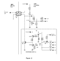
Figure 2 shows a sample circuit diagram of the power supply which comprises a security aimed protection circuit of the invention. - The present invention relates to a protection circuit and a method which protects the power supply by cutting the energy transmission in case of a short-circuit (error) at one of the outputs of the SMPS-type power supply. The method and circuit proposed by the present invention aims to ensure that the said protection circuit is activated in case of an error in SMPS.
- In case of an error, the SMPSs of the known art operate as follows: there is a switcher integrated circuit (IC) on the primary part of the SMPS. This switching circuit (IC) switches the power supply on and off according to the feedback signal transmitted by the optical binder (7). A parallel regulator (5) provides the optical binder (7) with the required current and thus it is ensured that the isolated feedback signal is transmitted to the switcher integrated circuit (IC) on the primary part. In case of an error, the parallel regulator (5) will conduct 0v to the optical binder (7) and this signal will be transmitted to the IC as a feedback signal by the optical binder (7) and IC will cut the power flow by shutting down the system.
- However, such a protection is not secure. The system cannot activate the protection mode in some instances and this causes the power supply to be damaged.
- The present invention comprises a protection circuit which controls the switcher integrated circuit (IC) on the primary part of the SMPS by means of the optical binder (7) and the regulator circuit (5) on the secondary part.
- The protection circuit of the present invention monitors the multi-output on the secondary side of the power supply and short circuits the regulator (5) on the secondary part of the power supply by means of a switch (3) and thus ensures that the integrated circuit (IC) on the primary part is off in the case that a short circuit takes place at any of these outputs.. It is ensured by this way that the power flow to the secondary part is cut off when a short-circuit take place and thus the power supply is protected.
- The protection circuit and working principle of the present invention is shown in the block diagram of
Figure 1 . The SMPS primary circuit (8), transformer (9), rectifiers and filters (10) which are provided on the secondary part of the supply isolate both the primary and secondary parts while at the same time the isolation circuit (optical binder) (7) which transmits the feedback signal received from the secondary part to the integrated circuit (IC) on the primary part, the parallel regulator which provides optical binder with feedback signal and the feedback network (5) received from the voltage outputs constitute the known components of an SMPS. - The protection circuit (A) of the invention comprises a NOR logic circuit (1) which commands the switch (3) to cut the power transmission in case of an error, controlling the output voltages which are connected thereto; a delay circuit (2) which prevents activation of the protection circuit for a period when the system is first activated; a switch (3) which is connected to the said NOR circuit and delay circuit and which cuts the power off by switching the integrated circuit (IC) off in case of an error; serial switches (4) (0205) which separate the output voltage lines from NOR circuit inputs and which are controlled by the stand-by signal coming from the micro controller.
- As can be seen in
Figure 1 , the function of the protection circuit (A) of the invention is performed as follows: - The output voltages on the secondary part of the SMPS are connected to the NOR logic controller circuit (2) and are monitored by this circuit. If any of the output voltages decrease, the NOR logic circuit sends a signal to the switch (3) to switch the integrated circuit (IC) on the primary part off. The switch (3) is controlled by the NOR controller circuit (1) and the delay circuit (2).
- Integrated circuits (IC) activate the protection mode in some SMPSs when the feedback line is an open circuit while they activate the protection mode in other SMPSs when the feedback line short circuits. The circuit of the invention can be used for both cases.
- Open-circuit switch (3) serial connected to the feedback line or short-circuit switch (3) parallel connected to the line and ground are added to the circuit accordingly.
- When the protection system (circuit) is active, the parallel switch, which is normally on, is switched off or the serial switch (3), which is normally off, is switched on in the case that a short circuit (0 Volt) takes place at any of the voltage outputs. When the short circuit is over, parallel switch (3) is on or the serial switch (3) is off. Thus the feedback cycle is accomplished and the SMPS is back to normal operation.
- When the feedback circuit first received energy, SMPS outputs will be 0 Volt. In order to prevent this situation from being misinterpreted as a short circuit, a delay circuit (2) connected to the NOR logic circuit (1) retards / inactivates the protection circuit (A) for a period required for the output voltages to reach the nominal value.
- Most electronic devices comprise a micro controller to manage the device in stand-by mode, and this micro controller monitors input sources such as the remote control, on-off button etc., opens the device, makes on-off checks on feedback circuits. An output of the micro controller generates stand-by signal. When the device to which the power supply (SMPS) is connected is in stand-by mode, some outputs of the SMPS (all the voltages except the required ones during stand-by mode will be cut off) will be zero voltage. In order that the protection circuit does not interpret this situation as a short circuit, on the inputs of the NOR controller circuit (1), to which each output voltage is connected, there are serial switches (4) (0205) which separate these lines from the NOR circuit inputs. These switches are controlled by the control signal (6) coming from the micro controller. During ordinary operation, the serial switches are off i.e. they transmit, and protection function applies to these lines as well. Since the switches are on during stand-by mode, protection function will not apply to these lines. The said switches (4) are preferably on the output voltages which are lowered during the stand-by mode of the SMPS (e.g. 12V line).
-
Figure 2 shows a sample circuit diagram of the protection circuit (A) of the invention. Q201 transistor on the circuit functions as a control switch (3). Q203 transistor and the connected resistors R213, R212, R214 and the capacitor C202 constitute the delay circuit (2). Q205 which is connected to the stand-by control signal (6) indicates the serial switches (4) to which the output voltages are connected. Q202, R210, R211, R215 and D201 constitute the NOR logic controller (1). There are serial connected diodes D202, D203, D204, D205 between the NOR controller inputs and voltage outputs. IC101 forms the optical binder (7) whereas IC201 and the peripheral units make up the parallel regulator and the feedback network (5). The known parts of the SMPS are not shown in the said circuit diagram. - The working principle of the protection circuit of the present invention, shown in
Figure 2 , is disclosed below: - Since the monitoring points of serial switches D202, D203, D204, D205, which are connected to the base circuit of the Q202 transistor of NOR controller circuit, are zero volt when circuit first receives energy, these diodes are in cutoff mode. Due to the fact that the C202 voltage, which is uncharged at first and is charged through R214, is zero volt, Q203 is in cutoff mode. Therefore 0201, through the base of which no current flows, is in cutoff mode. Thus Q201, a switch parallel connected between the feedback line and GND does not interfere in the feedback line and SMPS starts regular operation.
- Due to the fact that the monitoring points of D202, D203, D204 and D205 are at different voltages from zero volts during regular operation, Q202 is in conduction mode with the base current flowing through R215, D201, R211. Since now C202 is charged, Q203 is in conduction mode with the base current flowing through R214. Q203 and R212 generate the collector charge of Q202. As Q202 is in conduction mode, Q201 connected thereto is in cutoff mode. Therefore Q201, a switch parallel connected between the feedback line and GND does not interfere in the feedback line. Since the stand-by control signal is high during regular operation, Q205 is in conduction mode and the circuit monitoring function on 12V line is active.
- Approximately zero volt will be seen on the monitoring points of at least one of D202, D203, D204, D205 in case of a short circuit and NOR controller will be cutoff as the base current of Q202 is interrupted. Due to the base current flowing through Q203 and R212, Q201 enters conduction mode and forces the SMPS to enter the protection mode by short circuiting the feedback line to the reference ground. Therefore all the voltages are interrupted as SMPS is off and short circuit current does not flow any more. As long as there is short circuit on at least one of the monitoring points of D202, D203, D204 and D205, SMPS circuit will be forced to be off at each start attempt and protection function is accomplished during this period.
- When system enters stand-by mode, zero volt will be seen on some of the said output voltages (e.g. 12V line). Since the stand-by control signal, which is normally high, is lower in stand-by mode, Q205 enters cutoff mode and short circuit monitoring function will not apply on 12V line.
- The present invention can be applied to switched mode power supplies on any electronic device.
- The method and protection circuit of the invention both solves the high current (short circuit current) problems which may occur on the secondary part and brings solution to the heating problems which may take place on primary part in case of an error owing to the fact that the integrated circuit (IC) on the primary part is switched off.
Claims (9)
- A protection circuit (A) which controls a switcher integrated circuit (IC) on the primary part of a SMPS-type power supply by means of a regulator circuit (5) and an optical binder (7) on the secondary part; and which is also developed in order to protect the system by interrupting the energy transmission in the case that a short circuit takes place at any of the output voltages of the said power supply characterized in that it comprises- A NOR controller circuit (1) to which the output voltages of the power supply is connected,- A delay circuit (2) which deactivates the protection circuit (A) when the system, to which the power supply is connected, is first activated,- A switch (3) which is connected to the feedback line and which is controlled by NOR controller circuit (1) and delay circuit (2) in order to switch off the integrated circuit (IC) on the primary part in the case that a short circuit takes place at any of the output voltages,- Serial switches (4) which are controlled by the stand-by control signal (6) coming from the micro controller, and which separate the output voltages from NOR circuit inputs during stand-by.
- A protection circuit (A) according to Claim 1 characterized in that it comprises the diodes (D202, D203, D204, D205) which are between the said output voltages and NOR circuit inputs.
- A protection circuit (A) according to Claim 1 characterized in that it comprises a transistor between the output voltages of the said serial switches (4) and NOR controller circuit and which is connected to the stand-by control signal (6).
- A protection circuit (A) according to Claim 1 characterized in that it comprises a transistor serially connected to the feedback line of the said switch (3).
- A protection circuit (A) according to Claim 1 characterized in that it comprises a transistor parallel connected between feedback line of the said switch (3) and ground.
- A protection circuit (A) which controls a switcher integrated circuit (IC) on the primary part of a SMPS-type power supply by means of a regulator circuit (5) and an optical binder (7) on the secondary part; and which is also developed in order to protect the system by interrupting the energy transmission in the case that a short circuit takes place at any of the output voltages of the said power supply characterized in that it further comprises the steps of:- Monitoring the power supply output voltages by an NOR controller circuit (1),- Deactivation of the said protection method for a period by a delay circuit (2) when the system is first activated,- Separation of the output voltages from NOR circuit inputs by the serial switches (4) during stand-by,- Switching off the said integrated circuit (IC) by means of a switch (3) connected to the feedback line of the integrated circuit (IC)
- A method according to Claim 6 characterized in that the feedback line is short circuited by turning off the said switch (3) in the case that it is parallel connected between the feedback line and ground and any of the output voltages is short circuited; and the connection between the feedback line and ground is disconnected by turning on the switch when the short circuit is over.
- A method according to Claim 6 characterized in that the feedback line is transformed into an open circuit by turning on the said switch (3) in the case that it is serial connected between the feedback line and ground and any of the output voltages is short circuited; and reconnection is established by turning off the switch when the short circuit is over.
- A method according to Claim 6 characterized in that when the system is first activated the said protection method is retarded by the delay circuit (2) until the output voltages reach the nominal value.
Applications Claiming Priority (1)
| Application Number | Priority Date | Filing Date | Title |
|---|---|---|---|
| TR2009/00348A TR200900348A2 (en) | 2009-01-16 | 2009-01-16 | Protection circuit. |
Publications (2)
| Publication Number | Publication Date |
|---|---|
| EP2209196A1 true EP2209196A1 (en) | 2010-07-21 |
| EP2209196B1 EP2209196B1 (en) | 2014-03-19 |
Family
ID=42077788
Family Applications (1)
| Application Number | Title | Priority Date | Filing Date |
|---|---|---|---|
| EP10150134.4A Active EP2209196B1 (en) | 2009-01-16 | 2010-01-05 | Protection circuit for an isolated switch-mode power supply |
Country Status (3)
| Country | Link |
|---|---|
| EP (1) | EP2209196B1 (en) |
| ES (1) | ES2461150T3 (en) |
| TR (1) | TR200900348A2 (en) |
Cited By (1)
| Publication number | Priority date | Publication date | Assignee | Title |
|---|---|---|---|---|
| DE102014107019A1 (en) * | 2014-05-19 | 2015-11-19 | Fujitsu Technology Solutions Intellectual Property Gmbh | Power supply arrangement for an electronic device |
Citations (6)
| Publication number | Priority date | Publication date | Assignee | Title |
|---|---|---|---|---|
| US4270164A (en) | 1979-02-28 | 1981-05-26 | Contraves Goerz Corporation | Short circuit protection for switching type power processors |
| US6088244A (en) * | 1998-11-19 | 2000-07-11 | Yokogawa Electric Corp. | Switching power supply using a single isolating element to facilitate multiple functions |
| US20010009517A1 (en) | 2000-01-20 | 2001-07-26 | Peter Preller | Method for switching off a switched-mode power supply in the event of short-circuit, and a switched- mode power supply |
| EP1331722A1 (en) * | 2002-01-26 | 2003-07-30 | Thomson Licensing S.A. | Switched mode power supply |
| US20040201937A1 (en) * | 2003-04-08 | 2004-10-14 | Katsuyuki Yoshida | Overcurrent protection circuit for switching power supply |
| US20060028847A1 (en) * | 2004-08-05 | 2006-02-09 | Young-Chul Ryu | Switching mode power supply and switching controller thereof |
-
2009
- 2009-01-16 TR TR2009/00348A patent/TR200900348A2/en unknown
-
2010
- 2010-01-05 ES ES10150134.4T patent/ES2461150T3/en active Active
- 2010-01-05 EP EP10150134.4A patent/EP2209196B1/en active Active
Patent Citations (6)
| Publication number | Priority date | Publication date | Assignee | Title |
|---|---|---|---|---|
| US4270164A (en) | 1979-02-28 | 1981-05-26 | Contraves Goerz Corporation | Short circuit protection for switching type power processors |
| US6088244A (en) * | 1998-11-19 | 2000-07-11 | Yokogawa Electric Corp. | Switching power supply using a single isolating element to facilitate multiple functions |
| US20010009517A1 (en) | 2000-01-20 | 2001-07-26 | Peter Preller | Method for switching off a switched-mode power supply in the event of short-circuit, and a switched- mode power supply |
| EP1331722A1 (en) * | 2002-01-26 | 2003-07-30 | Thomson Licensing S.A. | Switched mode power supply |
| US20040201937A1 (en) * | 2003-04-08 | 2004-10-14 | Katsuyuki Yoshida | Overcurrent protection circuit for switching power supply |
| US20060028847A1 (en) * | 2004-08-05 | 2006-02-09 | Young-Chul Ryu | Switching mode power supply and switching controller thereof |
Cited By (2)
| Publication number | Priority date | Publication date | Assignee | Title |
|---|---|---|---|---|
| DE102014107019A1 (en) * | 2014-05-19 | 2015-11-19 | Fujitsu Technology Solutions Intellectual Property Gmbh | Power supply arrangement for an electronic device |
| US9935545B2 (en) | 2014-05-19 | 2018-04-03 | Fujitsu Technology Solutions Intellectual Property Gmbh | Power supply unit arrangement for an electronic device, power supply for an electronic device having at least a high-load state and a low-load state and computer system having a normal operating state and at least one energy saving state |
Also Published As
| Publication number | Publication date |
|---|---|
| ES2461150T3 (en) | 2014-05-16 |
| TR200900348A2 (en) | 2010-08-23 |
| EP2209196B1 (en) | 2014-03-19 |
Similar Documents
| Publication | Publication Date | Title |
|---|---|---|
| JP6101493B2 (en) | Power supply device, AC adapter, electronic device, and power supply system | |
| US10193458B2 (en) | Start-up controller for a power converter | |
| CN107528294B (en) | Power converter with load switch fault protection | |
| CN107346936B (en) | Switching Power Supply start-up circuit with the normal open device for providing starting charging current | |
| EP3258585B1 (en) | Isolated power converter with output voltage protection | |
| US6807075B2 (en) | Start-up circuit for switched mode power supply | |
| EP3249781B1 (en) | Selective protection circuit and method, and power supply system | |
| KR20130040657A (en) | Apparatus and method for protecting supply modulator | |
| US6804126B2 (en) | Power supply start up circuit | |
| KR20060012955A (en) | Switching mode power supplies and their switching controls | |
| CN105981276B (en) | Power converter with fast discharge circuit | |
| JP2009296790A (en) | Switching regulator | |
| EP2209196B1 (en) | Protection circuit for an isolated switch-mode power supply | |
| US10305275B2 (en) | Data interface with overvoltage protection for two-way digital control bus system | |
| US6151224A (en) | Power supply with reduced power comsumption in standby mode | |
| KR101067923B1 (en) | Switched-Mode Power Supplies with Soft-Start and Overload Protection | |
| KR102047826B1 (en) | Overvoltage protection circuit and power supply with the same | |
| EP3544148A1 (en) | Power reception device and power reception control method | |
| US11469660B2 (en) | Inrush current limiting power supply | |
| KR100721161B1 (en) | Feedback terminal circuit | |
| TW202333432A (en) | Conversion circuit and method of bootstrap voltage control the same | |
| EP3416271B1 (en) | Power supply apparatuses and methods with output control for multiple terminals | |
| EP0917281B1 (en) | Power supply with ecological stand by mode | |
| KR101993216B1 (en) | The power supply device and the method for supplying power | |
| KR102023675B1 (en) | The power supply device and the method for supplying power |
Legal Events
| Date | Code | Title | Description |
|---|---|---|---|
| PUAI | Public reference made under article 153(3) epc to a published international application that has entered the european phase |
Free format text: ORIGINAL CODE: 0009012 |
|
| AK | Designated contracting states |
Kind code of ref document: A1 Designated state(s): AT BE BG CH CY CZ DE DK EE ES FI FR GB GR HR HU IE IS IT LI LT LU LV MC MK MT NL NO PL PT RO SE SI SK SM TR |
|
| 17P | Request for examination filed |
Effective date: 20110118 |
|
| 17Q | First examination report despatched |
Effective date: 20121127 |
|
| GRAP | Despatch of communication of intention to grant a patent |
Free format text: ORIGINAL CODE: EPIDOSNIGR1 |
|
| INTG | Intention to grant announced |
Effective date: 20131111 |
|
| RIN1 | Information on inventor provided before grant (corrected) |
Inventor name: CESMECI, METE |
|
| GRAS | Grant fee paid |
Free format text: ORIGINAL CODE: EPIDOSNIGR3 |
|
| GRAA | (expected) grant |
Free format text: ORIGINAL CODE: 0009210 |
|
| AK | Designated contracting states |
Kind code of ref document: B1 Designated state(s): AT BE BG CH CY CZ DE DK EE ES FI FR GB GR HR HU IE IS IT LI LT LU LV MC MK MT NL NO PL PT RO SE SI SK SM TR |
|
| REG | Reference to a national code |
Ref country code: GB Ref legal event code: FG4D |
|
| REG | Reference to a national code |
Ref country code: CH Ref legal event code: EP |
|
| REG | Reference to a national code |
Ref country code: IE Ref legal event code: FG4D |
|
| REG | Reference to a national code |
Ref country code: AT Ref legal event code: REF Ref document number: 658239 Country of ref document: AT Kind code of ref document: T Effective date: 20140415 |
|
| REG | Reference to a national code |
Ref country code: DE Ref legal event code: R096 Ref document number: 602010014360 Country of ref document: DE Effective date: 20140430 |
|
| REG | Reference to a national code |
Ref country code: ES Ref legal event code: FG2A Ref document number: 2461150 Country of ref document: ES Kind code of ref document: T3 Effective date: 20140516 |
|
| PG25 | Lapsed in a contracting state [announced via postgrant information from national office to epo] |
Ref country code: LT Free format text: LAPSE BECAUSE OF FAILURE TO SUBMIT A TRANSLATION OF THE DESCRIPTION OR TO PAY THE FEE WITHIN THE PRESCRIBED TIME-LIMIT Effective date: 20140319 Ref country code: NO Free format text: LAPSE BECAUSE OF FAILURE TO SUBMIT A TRANSLATION OF THE DESCRIPTION OR TO PAY THE FEE WITHIN THE PRESCRIBED TIME-LIMIT Effective date: 20140619 |
|
| REG | Reference to a national code |
Ref country code: NL Ref legal event code: VDEP Effective date: 20140319 |
|
| REG | Reference to a national code |
Ref country code: AT Ref legal event code: MK05 Ref document number: 658239 Country of ref document: AT Kind code of ref document: T Effective date: 20140319 |
|
| REG | Reference to a national code |
Ref country code: LT Ref legal event code: MG4D |
|
| PG25 | Lapsed in a contracting state [announced via postgrant information from national office to epo] |
Ref country code: SE Free format text: LAPSE BECAUSE OF FAILURE TO SUBMIT A TRANSLATION OF THE DESCRIPTION OR TO PAY THE FEE WITHIN THE PRESCRIBED TIME-LIMIT Effective date: 20140319 Ref country code: CY Free format text: LAPSE BECAUSE OF FAILURE TO SUBMIT A TRANSLATION OF THE DESCRIPTION OR TO PAY THE FEE WITHIN THE PRESCRIBED TIME-LIMIT Effective date: 20140319 Ref country code: FI Free format text: LAPSE BECAUSE OF FAILURE TO SUBMIT A TRANSLATION OF THE DESCRIPTION OR TO PAY THE FEE WITHIN THE PRESCRIBED TIME-LIMIT Effective date: 20140319 |
|
| PG25 | Lapsed in a contracting state [announced via postgrant information from national office to epo] |
Ref country code: HR Free format text: LAPSE BECAUSE OF FAILURE TO SUBMIT A TRANSLATION OF THE DESCRIPTION OR TO PAY THE FEE WITHIN THE PRESCRIBED TIME-LIMIT Effective date: 20140319 Ref country code: LV Free format text: LAPSE BECAUSE OF FAILURE TO SUBMIT A TRANSLATION OF THE DESCRIPTION OR TO PAY THE FEE WITHIN THE PRESCRIBED TIME-LIMIT Effective date: 20140319 |
|
| PG25 | Lapsed in a contracting state [announced via postgrant information from national office to epo] |
Ref country code: BE Free format text: LAPSE BECAUSE OF FAILURE TO SUBMIT A TRANSLATION OF THE DESCRIPTION OR TO PAY THE FEE WITHIN THE PRESCRIBED TIME-LIMIT Effective date: 20140319 Ref country code: IS Free format text: LAPSE BECAUSE OF FAILURE TO SUBMIT A TRANSLATION OF THE DESCRIPTION OR TO PAY THE FEE WITHIN THE PRESCRIBED TIME-LIMIT Effective date: 20140719 Ref country code: NL Free format text: LAPSE BECAUSE OF FAILURE TO SUBMIT A TRANSLATION OF THE DESCRIPTION OR TO PAY THE FEE WITHIN THE PRESCRIBED TIME-LIMIT Effective date: 20140319 Ref country code: CZ Free format text: LAPSE BECAUSE OF FAILURE TO SUBMIT A TRANSLATION OF THE DESCRIPTION OR TO PAY THE FEE WITHIN THE PRESCRIBED TIME-LIMIT Effective date: 20140319 Ref country code: BG Free format text: LAPSE BECAUSE OF FAILURE TO SUBMIT A TRANSLATION OF THE DESCRIPTION OR TO PAY THE FEE WITHIN THE PRESCRIBED TIME-LIMIT Effective date: 20140619 Ref country code: EE Free format text: LAPSE BECAUSE OF FAILURE TO SUBMIT A TRANSLATION OF THE DESCRIPTION OR TO PAY THE FEE WITHIN THE PRESCRIBED TIME-LIMIT Effective date: 20140319 Ref country code: RO Free format text: LAPSE BECAUSE OF FAILURE TO SUBMIT A TRANSLATION OF THE DESCRIPTION OR TO PAY THE FEE WITHIN THE PRESCRIBED TIME-LIMIT Effective date: 20140319 |
|
| PG25 | Lapsed in a contracting state [announced via postgrant information from national office to epo] |
Ref country code: AT Free format text: LAPSE BECAUSE OF FAILURE TO SUBMIT A TRANSLATION OF THE DESCRIPTION OR TO PAY THE FEE WITHIN THE PRESCRIBED TIME-LIMIT Effective date: 20140319 Ref country code: SK Free format text: LAPSE BECAUSE OF FAILURE TO SUBMIT A TRANSLATION OF THE DESCRIPTION OR TO PAY THE FEE WITHIN THE PRESCRIBED TIME-LIMIT Effective date: 20140319 Ref country code: PL Free format text: LAPSE BECAUSE OF FAILURE TO SUBMIT A TRANSLATION OF THE DESCRIPTION OR TO PAY THE FEE WITHIN THE PRESCRIBED TIME-LIMIT Effective date: 20140319 |
|
| REG | Reference to a national code |
Ref country code: DE Ref legal event code: R097 Ref document number: 602010014360 Country of ref document: DE |
|
| PG25 | Lapsed in a contracting state [announced via postgrant information from national office to epo] |
Ref country code: PT Free format text: LAPSE BECAUSE OF FAILURE TO SUBMIT A TRANSLATION OF THE DESCRIPTION OR TO PAY THE FEE WITHIN THE PRESCRIBED TIME-LIMIT Effective date: 20140721 |
|
| PLBE | No opposition filed within time limit |
Free format text: ORIGINAL CODE: 0009261 |
|
| STAA | Information on the status of an ep patent application or granted ep patent |
Free format text: STATUS: NO OPPOSITION FILED WITHIN TIME LIMIT |
|
| PG25 | Lapsed in a contracting state [announced via postgrant information from national office to epo] |
Ref country code: DK Free format text: LAPSE BECAUSE OF FAILURE TO SUBMIT A TRANSLATION OF THE DESCRIPTION OR TO PAY THE FEE WITHIN THE PRESCRIBED TIME-LIMIT Effective date: 20140319 |
|
| 26N | No opposition filed |
Effective date: 20141222 |
|
| REG | Reference to a national code |
Ref country code: DE Ref legal event code: R097 Ref document number: 602010014360 Country of ref document: DE Effective date: 20141222 |
|
| PG25 | Lapsed in a contracting state [announced via postgrant information from national office to epo] |
Ref country code: SI Free format text: LAPSE BECAUSE OF FAILURE TO SUBMIT A TRANSLATION OF THE DESCRIPTION OR TO PAY THE FEE WITHIN THE PRESCRIBED TIME-LIMIT Effective date: 20140319 |
|
| REG | Reference to a national code |
Ref country code: CH Ref legal event code: PL |
|
| PG25 | Lapsed in a contracting state [announced via postgrant information from national office to epo] |
Ref country code: LU Free format text: LAPSE BECAUSE OF FAILURE TO SUBMIT A TRANSLATION OF THE DESCRIPTION OR TO PAY THE FEE WITHIN THE PRESCRIBED TIME-LIMIT Effective date: 20150105 |
|
| PG25 | Lapsed in a contracting state [announced via postgrant information from national office to epo] |
Ref country code: MC Free format text: LAPSE BECAUSE OF FAILURE TO SUBMIT A TRANSLATION OF THE DESCRIPTION OR TO PAY THE FEE WITHIN THE PRESCRIBED TIME-LIMIT Effective date: 20140319 |
|
| REG | Reference to a national code |
Ref country code: FR Ref legal event code: PLFP Year of fee payment: 7 |
|
| PG25 | Lapsed in a contracting state [announced via postgrant information from national office to epo] |
Ref country code: LI Free format text: LAPSE BECAUSE OF NON-PAYMENT OF DUE FEES Effective date: 20150131 Ref country code: CH Free format text: LAPSE BECAUSE OF NON-PAYMENT OF DUE FEES Effective date: 20150131 |
|
| REG | Reference to a national code |
Ref country code: IE Ref legal event code: MM4A |
|
| PG25 | Lapsed in a contracting state [announced via postgrant information from national office to epo] |
Ref country code: IE Free format text: LAPSE BECAUSE OF NON-PAYMENT OF DUE FEES Effective date: 20150105 |
|
| PG25 | Lapsed in a contracting state [announced via postgrant information from national office to epo] |
Ref country code: GR Free format text: LAPSE BECAUSE OF FAILURE TO SUBMIT A TRANSLATION OF THE DESCRIPTION OR TO PAY THE FEE WITHIN THE PRESCRIBED TIME-LIMIT Effective date: 20140620 |
|
| REG | Reference to a national code |
Ref country code: FR Ref legal event code: PLFP Year of fee payment: 8 |
|
| PG25 | Lapsed in a contracting state [announced via postgrant information from national office to epo] |
Ref country code: MT Free format text: LAPSE BECAUSE OF FAILURE TO SUBMIT A TRANSLATION OF THE DESCRIPTION OR TO PAY THE FEE WITHIN THE PRESCRIBED TIME-LIMIT Effective date: 20140319 |
|
| PG25 | Lapsed in a contracting state [announced via postgrant information from national office to epo] |
Ref country code: HU Free format text: LAPSE BECAUSE OF FAILURE TO SUBMIT A TRANSLATION OF THE DESCRIPTION OR TO PAY THE FEE WITHIN THE PRESCRIBED TIME-LIMIT; INVALID AB INITIO Effective date: 20100105 Ref country code: SM Free format text: LAPSE BECAUSE OF FAILURE TO SUBMIT A TRANSLATION OF THE DESCRIPTION OR TO PAY THE FEE WITHIN THE PRESCRIBED TIME-LIMIT Effective date: 20140319 |
|
| REG | Reference to a national code |
Ref country code: FR Ref legal event code: PLFP Year of fee payment: 9 |
|
| PG25 | Lapsed in a contracting state [announced via postgrant information from national office to epo] |
Ref country code: MK Free format text: LAPSE BECAUSE OF FAILURE TO SUBMIT A TRANSLATION OF THE DESCRIPTION OR TO PAY THE FEE WITHIN THE PRESCRIBED TIME-LIMIT Effective date: 20140319 |
|
| REG | Reference to a national code |
Ref country code: DE Ref legal event code: R082 Ref document number: 602010014360 Country of ref document: DE Representative=s name: LEONHARD, REIMUND, DIPL.-ING., DE Ref country code: DE Ref legal event code: R082 Ref document number: 602010014360 Country of ref document: DE Representative=s name: LEONHARD, REIMUND, DIPL.-ING., ES |
|
| PGFP | Annual fee paid to national office [announced via postgrant information from national office to epo] |
Ref country code: DE Payment date: 20250121 Year of fee payment: 16 |
|
| PGFP | Annual fee paid to national office [announced via postgrant information from national office to epo] |
Ref country code: ES Payment date: 20250225 Year of fee payment: 16 |
|
| PGFP | Annual fee paid to national office [announced via postgrant information from national office to epo] |
Ref country code: FR Payment date: 20250127 Year of fee payment: 16 |
|
| PGFP | Annual fee paid to national office [announced via postgrant information from national office to epo] |
Ref country code: IT Payment date: 20250129 Year of fee payment: 16 Ref country code: GB Payment date: 20250128 Year of fee payment: 16 |
|
| PGFP | Annual fee paid to national office [announced via postgrant information from national office to epo] |
Ref country code: TR Payment date: 20260105 Year of fee payment: 17 |