EP2209144A1 - Light emitting device package - Google Patents
Light emitting device package Download PDFInfo
- Publication number
- EP2209144A1 EP2209144A1 EP09180830A EP09180830A EP2209144A1 EP 2209144 A1 EP2209144 A1 EP 2209144A1 EP 09180830 A EP09180830 A EP 09180830A EP 09180830 A EP09180830 A EP 09180830A EP 2209144 A1 EP2209144 A1 EP 2209144A1
- Authority
- EP
- European Patent Office
- Prior art keywords
- light emitting
- emitting device
- package body
- package
- metal plate
- Prior art date
- Legal status (The legal status is an assumption and is not a legal conclusion. Google has not performed a legal analysis and makes no representation as to the accuracy of the status listed.)
- Granted
Links
Images




Classifications
-
- H—ELECTRICITY
- H10—SEMICONDUCTOR DEVICES; ELECTRIC SOLID-STATE DEVICES NOT OTHERWISE PROVIDED FOR
- H10H—INORGANIC LIGHT-EMITTING SEMICONDUCTOR DEVICES HAVING POTENTIAL BARRIERS
- H10H20/00—Individual inorganic light-emitting semiconductor devices having potential barriers, e.g. light-emitting diodes [LED]
- H10H20/80—Constructional details
- H10H20/85—Packages
- H10H20/858—Means for heat extraction or cooling
- H10H20/8582—Means for heat extraction or cooling characterised by their shape
-
- H—ELECTRICITY
- H10—SEMICONDUCTOR DEVICES; ELECTRIC SOLID-STATE DEVICES NOT OTHERWISE PROVIDED FOR
- H10H—INORGANIC LIGHT-EMITTING SEMICONDUCTOR DEVICES HAVING POTENTIAL BARRIERS
- H10H20/00—Individual inorganic light-emitting semiconductor devices having potential barriers, e.g. light-emitting diodes [LED]
- H10H20/80—Constructional details
- H10H20/85—Packages
- H10H20/857—Interconnections, e.g. lead-frames, bond wires or solder balls
-
- H—ELECTRICITY
- H10—SEMICONDUCTOR DEVICES; ELECTRIC SOLID-STATE DEVICES NOT OTHERWISE PROVIDED FOR
- H10W—GENERIC PACKAGES, INTERCONNECTIONS, CONNECTORS OR OTHER CONSTRUCTIONAL DETAILS OF DEVICES COVERED BY CLASS H10
- H10W70/00—Package substrates; Interposers; Redistribution layers [RDL]
- H10W70/60—Insulating or insulated package substrates; Interposers; Redistribution layers
- H10W70/67—Insulating or insulated package substrates; Interposers; Redistribution layers characterised by their insulating layers or insulating parts
- H10W70/68—Shapes or dispositions thereof
- H10W70/682—Shapes or dispositions thereof comprising holes having chips therein
-
- H—ELECTRICITY
- H10—SEMICONDUCTOR DEVICES; ELECTRIC SOLID-STATE DEVICES NOT OTHERWISE PROVIDED FOR
- H10W—GENERIC PACKAGES, INTERCONNECTIONS, CONNECTORS OR OTHER CONSTRUCTIONAL DETAILS OF DEVICES COVERED BY CLASS H10
- H10W72/00—Interconnections or connectors in packages
- H10W72/851—Dispositions of multiple connectors or interconnections
- H10W72/874—On different surfaces
- H10W72/884—Die-attach connectors and bond wires
-
- H—ELECTRICITY
- H10—SEMICONDUCTOR DEVICES; ELECTRIC SOLID-STATE DEVICES NOT OTHERWISE PROVIDED FOR
- H10W—GENERIC PACKAGES, INTERCONNECTIONS, CONNECTORS OR OTHER CONSTRUCTIONAL DETAILS OF DEVICES COVERED BY CLASS H10
- H10W90/00—Package configurations
- H10W90/701—Package configurations characterised by the relative positions of pads or connectors relative to package parts
- H10W90/731—Package configurations characterised by the relative positions of pads or connectors relative to package parts of die-attach connectors
- H10W90/734—Package configurations characterised by the relative positions of pads or connectors relative to package parts of die-attach connectors between a chip and a stacked insulating package substrate, interposer or RDL
Definitions
- Embodiments of the invention relate to a light emitting device package.
- a light emitting diode may constitute a light emitting source, and may use compound semiconductor materials such as GaAs-based materials, AlGaAs-based materials, GaN-based materials, InGaN-based materials and InGaAlP-based materials.
- Such an LED is packaged, and thereby is being used as a light emitting device for emitting various color lights.
- the light emitting device is being used as a light source in various fields, for example, lighting display devices, character display devices and image display devices.
- Embodiments of the invention provide a light emitting device package in which a thermal resistance is improved.
- Embodiments of the invention provide a light emitting device package in which a heat-radiating path of a light emitting device is improved.
- An embodiment of the invention provides a light emitting device package including a package body comprising a cavity disposed at an upper portion; an insulating layer disposed on a surface of the package body; a plurality of metal layers disposed on the insulating layer; a light emitting device disposed in the cavity; and a first metal plate disposed on a rear surface of the package body at a location corresponding to the light emitting device.
- An embodiment of the invention provides a light emitting device package including a package body having a cavity; a plurality of metal layers disposed on the package body; an insulating layer disposed between the plurality of metal layers and the package body; at least one well formed in the package body; a light emitting device disposed on the package body in the cavity; and a first metal plate disposed under the package body at a region corresponding to the light emitting device
- An embodiment of the invention provides a light emitting device package including a package body having a cavity, and formed of a silicon material; at least one light emitting device disposed in the cavity of the package body; and a first metal plate disposed at a region corresponding to a region of the light emitting device at an under surface of the package body.
- Fig. 1 is a cross-sectional view illustrating a light emitting device package according to a first embodiment.
- Figs. 2A and 2B are diagrams respectively illustrating a heat-radiating path and a heat-radiating resistor corresponding to the light emitting device package in Fig.1 .
- Fig. 3 is a circuit diagram illustrating an example of the equivalent circuit of the light emitting device package in Fig. 1 .
- Fig. 4 is a circuit diagram illustrating another example of the equivalent circuit of the light emitting device package in Fig. 1 .
- Figs. 5 to 11 are diagrams illustrating a method for manufacturing the light emitting device package in Fig. 1 .
- Fig. 12 is a side-sectional view illustrating a light emitting device package according to a second embodiment.
- Figs. 13A and 13B are diagrams respectively illustrating a heat-radiating path and a heat-radiating resistor corresponding to the light emitting device package in Fig. 12 .
- Fig. 14 is a side-sectional view illustrating a light emitting device package according to a third embodiment.
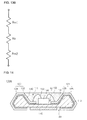
- Figs. 15A, 15B and 15C are diagrams respectively illustrating a heat-radiating path, a heat-radiating resistor and a circuit configuration corresponding to the light emitting device package in Fig. 14 .
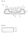
- Fig. 16 is a side-sectional view illustrating a light emitting device package according to a fourth embodiment.
- Figs. 17A , 17B and 17C are diagrams respectively illustrating a heat-radiating path, a heat-radiating resistor and a circuit configuration corresponding to the light emitting device package in Fig.16 .
- Fig. 1 is a cross-sectional view illustrating a light emitting device package according to a first embodiment.
- a light emitting device package 100 includes a package body 110, insulating layers 120 and 121, a plurality of wells (or doped regions) 131 to 134, first and second metal layers 140 and 141, a metal plate 145, and a light emitting device 150.
- the package body 110 may be formed with a conductive substrate or a Wafer Level Package (WLP) using a silicon material.
- a cavity 111 having a certain depth is formed at the upper portion of the package body 110.
- the cavity 111 may be formed as any one of a concave base tube shape, a concave polygonal shape and a concave circular shape. Other shapes are within the scope of the invention.
- the side surface of the cavity 111 of the package body 110 may be formed to be inclined, to be vertical at a certain angle, to have a certain curvature, or to have a step, for example.
- the perimeter of the top of the package body 110 may be formed to be flat, and the outside surfaces of the package body 110 may be formed to be bent at a certain angle, formed to be inclined, to be vertical at a certain angle, to have a certain curvature, or to have a step, for example.
- the insulating layers 120 and 121 are formed on a surface of the package body 110.
- the insulating layers 120 and 121 may be formed of at least one of insulating material or dielectric materials such as silicon thermal oxide, silicon carbide (SiC), aluminum nitride (AIN), alumina and silicon nitride.
- the insulating layers 120 and 121 may be formed of the silicon thermal oxide for forming a Zener diode structure in the package body 110.
- the region between the cavity 111 and the rear surface of the package body 110 may be formed to have a minimum thickness.
- the thickness between the bottom of the cavity 111 and the rear surface of the package body 110 for example, is about 500 um to about 2000 um.
- the thickness may be altered according to heat transfer efficiency without causing the breakage of a silicon wafer.
- a 1Ath insulating layer 122 and a 1Bth insulating layer 124 are integrally formed on an inclined side of the package body 110 in the cavity 111 and an inclined outside surface of the package body 110, respectively.
- the 1 Bth insulating layer 124 extends on the inclined outside surface and a portion of the under surface of the package body 110.
- the side of the package body 110 having the first insulating layer 120 may be referred to as a first side of the package body 110.
- a 2Ath insulating layer 123 and a 2Bth insulating layer 125 are integrally formed on an inclined side of the package body 110 in the cavity 111 and an inclined outside surface of package body 110 on the other side of the package body 110 from the first insulating layer 120.
- the 2Bth insulating layer 125 extends on the inclined outside surface and a portion of the rear surface of the package body 110 on the other side of the package body 110 from the first insulating layer 120.
- the side of the package body 110 having the second insulating layer 121 may be referred to as a second side of the package body 110.
- the first and second insulating layers 120 and 121 may be integrally formed at a region other than an open region A1 of the bottom of the cavity 111 and an open region A3 of the rear surface of the package body 110, or may be disposed under the first and second metal layers 140 and 141.
- the wells (or doped regions) 131 to 134 are formed at certain regions of the package body 110, respectively.
- a first well 131 is formed at the first side of the package body 110, and a second well 132 is formed at the second side of the package body 110.
- a third well 133 is formed at the cavity 111 of the package body 110, and a fourth well 134 is formed at the rear surface of the package body 110.
- the first well 131 is formed in the package body 110 at an open region (or an opening) of the first insulating layer 120
- the second well 132 is formed in the package body 110 at an open region (or an opening) of the second insulating layer 121.
- the first and second wells 131 and 132 may be formed by diffusing or injecting impurities into the package body 110.
- the diffused or injected impurities have a polarity that is opposite to the polarity of the package body 110, for example, the polarity of a silicon substrate.
- the first and second wells 131 and 132 may be realized as (or used in) Zener diodes that are formed in the package body 110.
- the third well 133 is disposed at the bottom of the cavity 111, and the fourth well 134 is formed at the under surface of the opposite side of the third well 133.
- the third and fourth well 133 and 134 may also be formed by diffusing or injecting the same types of impurities as the first and second wells 131 and 132 into the package body 110.
- the third well 133 is formed at the package body 110 that is exposed at the open region A1 of a center portion of the cavity 111
- the fourth well 134 is formed at the package body 110 that is exposed at the open region A3 of the rear surface of the package body 110.
- the third well 133 or/and the fourth well 134 is/are electrically insulated from the light emitting device 150 (i.e., a floating state), and thus may be realized as a constant-current transistor and a Zener diode for other device protection.
- the first and second insulating layers 120 and 121 may be a single continuous or contiguous insulating layer that covers the entire surface or most of the surface of the package body 110, which may be formed with a conductive substrate or a Wafer Level Package (WLP) using the silicon material.
- WLP Wafer Level Package
- one or more openings may be formed for use in forming the wells (i.e., the doped regions) in the package body 110.
- the first and second metal layers 140 and 141 having certain patterns are formed on the first and second insulating layers 120 and 121, respectively. Moreover, the first and second metal layers 140 and 141 are electrically insulated from each other, for example, by the open regions A1 and A3 of the package body 110, and are formed at a region of the cavity 111 and a portion of each of the top, side and under surfaces of the package body 110. Accordingly, where the first and second metal layers 140 and 141 are divided, an underlying portion of the insulating layer (e.g., 120 and 121) may be exposed.
- the first and second metal layers 140 and 141 each may be formed as a single layer or multi-layers of metal by using at least one of copper (Cu), nickel (Ni), gold (Au) and titanium (Ti), but they are not limited thereto.
- the first and second metal layers 140 and 141 may be used as two electrode leads, and the number of the leads may be varied according to a metal-layer pattern.
- a portion of the first metal layers 140 is formed on the first well 131 and thereby is electrically connected to the first well 131.
- the second metal layer 141 is formed on the second well 132 and thereby is electrically connected to the second well 132.
- the light emitting device 150 is mounted within the cavity 111 of the package body 110. At least one chip or at least one kind of chip may be mounted on the light emitting device 150.
- the light emitting device 150 is attached to the bottom (i.e., the surface of the package body) of the cavity 111.
- the light emitting device 150 may be a colored LED chip such as a blue LED chip, a green LED chip, a red LED chip and/or a yellow LED chip, or may be an ultraviolet (UV) LED chip.
- UV ultraviolet
- the light emitting device 150 may be attached onto the third well 133 that is formed at the open region A1 of the cavity 111 of the package body 110.
- the first and second metal layers 140 and 141 and the light emitting device 150 are electrically connected with a plurality wires 152.
- the package body 110 may be solder-bonded to a base substrate (for example, MOPCB) at the under and side surfaces thereof using Surface Mount Technology (SMT).
- a base substrate for example, MOPCB
- SMT Surface Mount Technology
- first and second wells 131 and 132 are connected to the light emitting device 150 in parallel, or the first and second wells 131 and 132 and the light emitting device 150 may be formed as independent devices, according to the patterns of the first and second metal layers 140 and 141.
- the third metal plate 145 is formed at the open region A3 of the rear surface of the package body 110.
- the third metal plate 145 may be formed of the same material as that of the first and second metal layers 140 and 141, or may be formed of another metal material having good heat radiation characteristic.
- the third metal plate 145 is formed at a region facing the bottom of the light emitting device 150, for example, under the fourth well 134.
- the third metal plate 145 radiates heat that is produced from the light emitting device 150.
- the third metal plate 145 may be effective for radiating heat when its size is formed to be greater than the contact-surface area of the light emitting device 150.
- the thickness of the third metal plate 145 may be formed to about 0.5 um to about 100 um, but it is not limited thereto.
- the light emitting device 150 and the third metal plate 145 are place on opposing surfaces of the package body 110.
- the contact area of the light emitting device 150 on the package body 110 is smaller than a contact area of the third metal plate 145 on the package body 110, but is not limited thereto.
- the light emitting device 150 and the third metal plate 145 are place on opposing surfaces of a thinnest part of the package body 110.
- the third metal plate 145 and the under surface of the package body 110 may be formed on the same plane.
- the third metal plate 145 is disposed in a structure where it is electrically opened to the first and second metal layers 140 and 141.
- a resin material 160 is formed at the cavity 111.
- the resin material 160 may be formed of a transparent resin material such as silicon or an epoxy. Moreover, at least one kind of phosphor may be contained to the resin material 160, but it is not limited thereto.
- the light emitting device 150 When a power source is attached, and power (e.g., current) is supplied through the first and second metal layers 140 and 141, the light emitting device 150 receives the power through the wire 152, which is connected to the first and second metal layers 140 and 141, to emit light.
- power e.g., current
- the package body 110 When heat is produced by driving of the light emitting device 150, a portion of the heat is conducted to the third metal plate 145 through the package body 110 beneath the light emitting device 150, and is thereby radiated. At this point, because the thickness of a region at which the third metal plate 145 is formed is thin, the package body 110 can effectively conduct heat. The heat is purposely conducted through the thin region of the package body 110 to the third metal place 145 because the heat transferred to parts of the package body other than where the third metal place 145 is located will not effectively radiate due to the presence of the insulating layers 120 and 121.
- Figs. 2A and 2B are diagrams respectively illustrating a heat-radiating path and a heat-radiating resistor of Fig. 1 .
- heat produced in the light emitting device 150 is transferred through the package body 110 and the third metal plate 145 that are disposed underneath the light emitting device 150 and is thereby radiated. That is, the heat produced in the light emitting device 150 is transferred through the package body 110 and the third metal plate 145 and is thereby radiated to the outside.
- the resistor Rs of the package body 110 and the resistor Rm of the third metal plate 145 are connected as the thermal resistors of the semiconductor emitting device package.
- the heat of the light emitting device 120 can be quickly radiated by the thermal resistors Rs and Rm. This reduces the number of the thermal resistors Rs and Rm that are disposed at the vertical down direction of the light emitting device 150, and thus a high-efficiency package can be manufactured. Accordingly, the light emitting device 150 stably operates, improving light emission efficiency.
- Fig. 3 is a circuit diagram illustrating an example of the equivalent circuit of the light emitting device package in Fig.1 .
- the light emitting device package includes a light emitting diode D1 and a Zener diode ZD1.
- the light emitting diode D1 and the Zener diode ZD1 may be connected in parallel.
- First and second electrodes P1 and P2 are connected to opposite ends of the light emitting diode D1 and the Zener diode ZD1, respectively.
- Zener diode ZD1 has been disclosed as a bi-directional Zener diode having a bi-directional threshold voltage
- a uni-directional Zener diode having a uni-directional threshold voltage may be connected to the light emitting diode D1 in anti-parallel, and it may be selectively used within the spirit and scope of the above-described technology.
- anti-parallel or inverse-parallel refers to an arrangement of devices that are connected in parallel but with their polarities reversed.
- Fig. 4 is a circuit diagram illustrating another example of the equivalent circuit of the light emitting device package in Fig. 1 .
- the light emitting device package includes a light emitting diode D1, a first Zener diode ZD1, and a second Zener diode ZD2.
- the light emitting diode D1 and the first Zener diode ZD1 may be connected in parallel, and the second Zener diode ZD2 is configured as a circuit that differs from the first Zener diode ZD1. That is, the first and second wells 131 and 132 in Fig. 1 may be realized as the first Zener diode ZD1, and the third and fourth wells 133 and 134 in Fig. 1 may be realized as the second Zener diode ZD2.
- Figs. 5 to 11 are diagrams illustrating a method for manufacturing the light emitting device package in Fig. 1 .
- the package body 110 may be formed with a conductive substrate or a WLP using a silicon material.
- the cavity 111 having a certain depth is formed at the upper portion of the package body 110.
- a mask pattern is formed on and under the package body 110 and the cavity 111 may be formed through an etching process.
- the etching process may use a wet etching process or a dry etching process.
- the surface of cavity 111 may be formed as a concave base tube shape, a concave polygonal shape or a concave circular shape, but is not limited thereto.
- the side surface of the cavity 111 may be formed to be inclined, to be vertical at a certain angle, to be at a certain curvature, or to have a step, for example.
- the perimeter of the top of the package body 110 may be formed to be flat, and the opposite side surfaces of the package body 110 may be formed to be bent at a certain angel.
- the region between the cavity 111 and the under surface of the package body 110 may be formed to a minimum thickness of the package body 110.
- the thickness between the bottom of the cavity 111 and the under surface of the package body 110 for example, is about 500 um to about 2000 um.
- the thickness may be altered according to heat transfer efficiency without causing breakage of a silicon wafer (the package body 110).
- an insulating layer 120A is formed on the entire surface of the package body 110, but is not limited thereto.
- the insulating layer 120A may be formed of at least one of dielectric materials, such as silicon thermal oxide, SiC, AIN, alumina and silicon nitride, or may use a dielectric material that is used in a silicon semiconductor process.
- the insulating layer 120A may be used as a silicon thermal oxide.
- a patterning process is performed on the insulating layer 120A.
- the insulating layer 120A By forming the open region A1 of the cavity 111 and the both-side well open region A2 and rear-surface open region A3 of the package body 110 through the patterning process via removal of portions of the insulating layer 120A, the insulating layer 120A is opened. Accordingly, the insulating layer 120A may be disposed as the first and second insulating layers 120 and 121 by the patterning process.
- the first and second insulating layers 120 and 121 may be integrally formed or may be disposed in a divided structure.
- the 1Ath insulating layer 122 and the 1Bth insulating layer 124 are integrally formed at the one side (the first side) of the cavity 111 of the package body 110 and the one side (the first side) of the body of the package body 110.
- the 1Bth insulating layer 124 is extended to the one-side (the first side) surface of the package body 110 and a portion of the rear surface of the package body 110.
- the 2Ath insulating layer 123 and the 2Bth insulating layer 125 are integrally formed at the other side (the second side) of the cavity 111 of the package body 110 and the other side (the second side) of the body of the package body 110.
- the 2Bth insulating layer 125 is extended to the other-side (the second side) surface of the package body 110 and a portion of the under surface of the package body 110.
- the first and second insulating layers 120 and 121 may be integrally formed at a region other than the open region A1 of the bottom of the cavity 111 and the open region A3 of the rear surface of the package body 110, or may be divided in plurality.
- a diffusion process is performed on the open regions A1 to A3 from which the insulating layers 120 and 121 has been removed.
- the diffusion process is a process that diffuses impurities into the package body 110 through the open regions A1 to A3, wherein the impurities opposite to the polarity of a silicon substrate are injected or doped. Accordingly, the first to fourth wells (or doped regions) 131 to 134 are formed at the package body 110 of the open regions A1 to A3.
- the first well 131 is formed at the one-side (the first side) open region A2 of the package body 110
- the second well 132 is formed at the other-side (the second side) open region A2 of the package body 110.
- the third well 133 is formed at the open region A1 of the cavity 111 of the package body 110
- the fourth well 134 is formed at the rear-surface open region A3 of the package body 110.
- the first and second wells 131 and 132 may be realized as Zener diodes, and the third and fourth wells 133 and 134 may be realized as Zener diodes for other device protection.
- the third well 133 or/and the fourth well 134 is/are electrically insulated from the light emitting device 150 (i.e., a floating state), and thus may be realized as a constant-current transistor and a Zener diode for other device protection.
- a metal forming process is performed.
- the first and second metal layers 140 and 141 and the third metal plate 145 are formed using a mask pattern in a sputtering process or a thin film deposition process, but is not limited thereto.
- the first and second metal layers 140 and 141 are formed on the insulating layers 120 and 121, and the third metal plate 145 is formed at the under-surface open region A3 of the package body 110.
- the first and second metal layers 140 and 141 are electrically opened, and are extended to the region of the cavity 111 and a portion of the side surface and under surface of the package body 110.
- the third metal plate 145 may serve as an under-surface heat radiating plate.
- the first and second metal layers 140 and 141 may be used as at least two electrode leads, and the number of the leads may be varied according to a metal-layer pattern.
- the first and second metal layers 140 and 141 and the third metal plate 145 may be formed in the same process and may be formed as single layers or multi layers by using at least one of Cu, Ni, Au and Ti, but they are not limited thereto.
- the third metal plate 145 is formed under the fourth well 134.
- the third metal plate 145 may be effective for radiating heat.
- the thickness of the third metal plate 145 may be formed to about 0.5 um to about 100 um, but it is not limited thereto.
- the first and second metal layers 140 and 141 are formed on the first and second wells 131 and 132, and are electrically connected to the first and second wells 131 and 132.
- a process is performed which mounts the light emitting device 150.
- the light emitting device 150 is attached in the cavity 111 of the package body 110. At least one the light emitting 150 may be disposed on the third well 133.
- the light emitting device 150 is electrically connected to the first and second metal layers 140 and 141 through the plurality of wires 152, but such a connection scheme is not limited thereto.
- the light emitting device 150 may be a colored LED chip such as a blue LED chip, a green LED chip, a red LED chip and/or a yellow LED chip, or may be realized as an ultraviolet (UV) LED chip.
- the kind and number of the light emitting device 150 are not limited thereto.
- first and second wells 131 and 132 and the light emitting device 150 may be formed as a parallel circuit or may be formed as independent circuits, according to the patterns of the first and second metal layers 140 and 141.
- the resin material 160 is formed in the cavity 111.
- the resin material 160 may be formed of a transparent resin material such as silicon or an epoxy, or at least one kind of phosphor may be contained to the resin material 160.
- a lens may be formed or is attached on the cavity 111, but is not limited thereto.
- the first and second metal layers 140 and 141 may be solder bonded to a base substrate (for example, MOPCB) at the under and side surfaces of the package body 110 in SMT.
- a base substrate for example, MOPCB
- Fig. 12 is a side-sectional view illustrating a light emitting device package according to a second embodiment.
- Figs. 13A and 13B are diagrams respectively illustrating the heat-radiating path and the heat-radiating resistor corresponding to the light emitting device package in Fig. 12 .
- repetitive description on the same elements as those of the first embodiment will be omitted and reference will be made to the first embodiment.
- a fourth metal plate 147 is formed on the third well 133 of the package body 110, and a third metal plate 145 is formed under the fourth well 134.
- Heat radiated from the light emitting device 150 is radiated along the fourth metal plate 147, the package body 110 and the third metal plate 145.
- the third and fourth metal plates 145 and 147 are electrically disconnected from the first and second metal plates 140 and 141.
- the size of the fourth metal plate 145 may be formed to be greater than the contact-surface area of the light emitting device 150, but is not limited thereto.
- the light emitting device 150 can stably operate, thereby improving the reliability of the light emitting device package.
- Fig. 14 is a side-sectional view illustrating a light emitting device package according to a third embodiment.
- Figs. 15A, 15B and 15C are diagrams respectively illustrating a heat-radiating path, a heat-radiating resistor and a circuit configuration corresponding to the light emitting device package in Fig. 14 .
- repetitive description on the same elements as those of the first embodiment will be omitted and reference will be made to the first embodiment.
- a light emitting device package 100B has a structure in which a well (or a doped region) is not formed at the package body 110.
- the light emitting device 150 is attached to the open region A1 of the bottom of the cavity 111 of the package body 110.
- the third metal plate 145 is formed at an under-surface open region A3.
- a heat-radiating resistor has a structure in which a package body resistor Rs and a third metal plate resistor Rm are connected.
- a well is not formed from the package body 110, only a light emitting device D1 is included.
- Fig. 16 is a side-sectional view illustrating a light emitting device package according to a fourth embodiment.
- Figs. 17A , 17B and 17C are diagrams respectively illustrating a heat-radiating path, a heat-radiating resistor and a circuit configuration corresponding to the light emitting device package in Fig. 16 .
- repetitive description on the same elements as those of the third embodiment will be omitted and reference will be made to the third embodiment.
- a fourth metal plate 137 is disposed under a light emitting device 150 and is disposed at the bottom of the cavity 111 of the package body 110.
- a third metal plate 145 is disposed at the under-surface open region A3 of the package body 110.
- a heat-radiating resistor in a heat-radiating path, heat produced from the light emitting device 150 is radiated through the fourth metal plate 137, the package body 110 and the third metal plate 145.
- a heat-radiating resistor includes a fourth metal plate resistor Rm1, a package body resistor Rs and a third metal plate resistor Rm2. The heat is conducted trough the heat-radiating resistors Rm1, Rs and Rm2.
- the light emitting device package is configured with a circuit including a light emitting diode D1.
- a metal plate or/and a well is/are disposed at the cavity 111 of the package body 110, and a metal plate or/and a well is/are disposed at a surface opposite to this. Accordingly, radiant heat can be induced by the minimum number of resistors, and a protection device can be manufactured.
- the heat-transferring path of the light emitting device is improved in the semiconductor emitting device package, improving the light emission efficiency of the light emitting device.
- the light emitting device can be protected from an abnormal power source.
- heat radiation efficiency can improve by about 5 % to about 20 % in the semiconductor emitting device package.
- the reliability of the semiconductor emitting device package can improve.
- An embodiment of the invention provides a method for manufacturing a light emitting device package including forming a cavity at a package body; forming an insulating layer at a surface of the package body; forming a plurality of metal layers on the insulating layer; forming a metal plate under the package body; attaching a light emitting device on the package body in the cavity; and electrically connecting the light emitting device to the metal layers.
Landscapes
- Led Device Packages (AREA)
Abstract
Description
- Embodiments of the invention relate to a light emitting device package.
- A light emitting diode (LED) may constitute a light emitting source, and may use compound semiconductor materials such as GaAs-based materials, AlGaAs-based materials, GaN-based materials, InGaN-based materials and InGaAlP-based materials.
- Such an LED is packaged, and thereby is being used as a light emitting device for emitting various color lights. The light emitting device is being used as a light source in various fields, for example, lighting display devices, character display devices and image display devices.
- Embodiments of the invention provide a light emitting device package in which a thermal resistance is improved.
- Embodiments of the invention provide a light emitting device package in which a heat-radiating path of a light emitting device is improved.
- An embodiment of the invention provides a light emitting device package including a package body comprising a cavity disposed at an upper portion; an insulating layer disposed on a surface of the package body; a plurality of metal layers disposed on the insulating layer; a light emitting device disposed in the cavity; and a first metal plate disposed on a rear surface of the package body at a location corresponding to the light emitting device.
- An embodiment of the invention provides a light emitting device package including a package body having a cavity; a plurality of metal layers disposed on the package body; an insulating layer disposed between the plurality of metal layers and the package body; at least one well formed in the package body; a light emitting device disposed on the package body in the cavity; and a first metal plate disposed under the package body at a region corresponding to the light emitting device
- An embodiment of the invention provides a light emitting device package including a package body having a cavity, and formed of a silicon material; at least one light emitting device disposed in the cavity of the package body; and a first metal plate disposed at a region corresponding to a region of the light emitting device at an under surface of the package body.
- The details of one or more embodiments of the invention are set forth in the accompanying drawings and the description below. Other features will be apparent from the description and drawings, and from the claims.
-
Fig. 1 is a cross-sectional view illustrating a light emitting device package according to a first embodiment. -
Figs. 2A and 2B are diagrams respectively illustrating a heat-radiating path and a heat-radiating resistor corresponding to the light emitting device package inFig.1 . -
Fig. 3 is a circuit diagram illustrating an example of the equivalent circuit of the light emitting device package inFig. 1 . -
Fig. 4 is a circuit diagram illustrating another example of the equivalent circuit of the light emitting device package inFig. 1 . -
Figs. 5 to 11 are diagrams illustrating a method for manufacturing the light emitting device package inFig. 1 . -
Fig. 12 is a side-sectional view illustrating a light emitting device package according to a second embodiment. -
Figs. 13A and13B are diagrams respectively illustrating a heat-radiating path and a heat-radiating resistor corresponding to the light emitting device package inFig. 12 . -
Fig. 14 is a side-sectional view illustrating a light emitting device package according to a third embodiment. -
Figs. 15A, 15B and 15C are diagrams respectively illustrating a heat-radiating path, a heat-radiating resistor and a circuit configuration corresponding to the light emitting device package inFig. 14 . -
Fig. 16 is a side-sectional view illustrating a light emitting device package according to a fourth embodiment. -
Figs. 17A ,17B and 17C are diagrams respectively illustrating a heat-radiating path, a heat-radiating resistor and a circuit configuration corresponding to the light emitting device package inFig.16 . - Reference will now be made in detail to the embodiments of the invention, examples of which are illustrated in the accompanying drawings. In description of embodiments, the 'on' or 'under' of each layer may be described with reference to the accompanying drawings, and the thickness of the each layer will also be described as an example and is not limited to the thickness of the accompanying drawings.
- In the description of embodiments, it will be understood that when a layer (or film), region, pattern or structure is referred to as being 'on' or 'under' another layer (or film), region, pad or pattern, the terminology of 'on' and 'under' includes both the meanings of 'directly' and 'indirectly'. Further, the reference about 'on' and 'under' each layer will be made on the basis of drawings. Also, the thickness of each layer in the drawings is an example, and is not limited thereto.
-
Fig. 1 is a cross-sectional view illustrating a light emitting device package according to a first embodiment. Referring toFig. 1 , a lightemitting device package 100 includes apackage body 110,insulating layers second metal layers metal plate 145, and alight emitting device 150. - The
package body 110 may be formed with a conductive substrate or a Wafer Level Package (WLP) using a silicon material. Acavity 111 having a certain depth is formed at the upper portion of thepackage body 110. Thecavity 111 may be formed as any one of a concave base tube shape, a concave polygonal shape and a concave circular shape. Other shapes are within the scope of the invention. - The side surface of the
cavity 111 of thepackage body 110 may be formed to be inclined, to be vertical at a certain angle, to have a certain curvature, or to have a step, for example. The perimeter of the top of thepackage body 110 may be formed to be flat, and the outside surfaces of thepackage body 110 may be formed to be bent at a certain angle, formed to be inclined, to be vertical at a certain angle, to have a certain curvature, or to have a step, for example. - The
insulating layers package body 110. Theinsulating layers insulating layers package body 110. - In the
package body 110, the region between thecavity 111 and the rear surface of thepackage body 110 may be formed to have a minimum thickness. The thickness between the bottom of thecavity 111 and the rear surface of thepackage body 110, for example, is about 500 um to about 2000 um. The thickness may be altered according to heat transfer efficiency without causing the breakage of a silicon wafer. - In the first
insulating layer 120, a1Ath insulating layer 122 and a1Bth insulating layer 124 are integrally formed on an inclined side of thepackage body 110 in thecavity 111 and an inclined outside surface of thepackage body 110, respectively. Herein, the 1Bth insulating layer 124 extends on the inclined outside surface and a portion of the under surface of thepackage body 110. The side of thepackage body 110 having the first insulatinglayer 120 may be referred to as a first side of thepackage body 110. - In the second
insulating layer 121, a2Ath insulating layer 123 and a2Bth insulating layer 125 are integrally formed on an inclined side of thepackage body 110 in thecavity 111 and an inclined outside surface ofpackage body 110 on the other side of thepackage body 110 from the firstinsulating layer 120. Herein, the2Bth insulating layer 125 extends on the inclined outside surface and a portion of the rear surface of thepackage body 110 on the other side of thepackage body 110 from the firstinsulating layer 120. The side of thepackage body 110 having the secondinsulating layer 121 may be referred to as a second side of thepackage body 110. - The first and second
insulating layers cavity 111 and an open region A3 of the rear surface of thepackage body 110, or may be disposed under the first andsecond metal layers - The wells (or doped regions) 131 to 134 are formed at certain regions of the
package body 110, respectively. Afirst well 131 is formed at the first side of thepackage body 110, and asecond well 132 is formed at the second side of thepackage body 110. Athird well 133 is formed at thecavity 111 of thepackage body 110, and afourth well 134 is formed at the rear surface of thepackage body 110. - The
first well 131 is formed in thepackage body 110 at an open region (or an opening) of the firstinsulating layer 120, and thesecond well 132 is formed in thepackage body 110 at an open region (or an opening) of thesecond insulating layer 121. The first andsecond wells package body 110. The diffused or injected impurities have a polarity that is opposite to the polarity of thepackage body 110, for example, the polarity of a silicon substrate. The first andsecond wells package body 110. - The
third well 133 is disposed at the bottom of thecavity 111, and thefourth well 134 is formed at the under surface of the opposite side of thethird well 133. The third andfourth well second wells package body 110. - The
third well 133 is formed at thepackage body 110 that is exposed at the open region A1 of a center portion of thecavity 111, and thefourth well 134 is formed at thepackage body 110 that is exposed at the open region A3 of the rear surface of thepackage body 110. The third well 133 or/and thefourth well 134 is/are electrically insulated from the light emitting device 150 (i.e., a floating state), and thus may be realized as a constant-current transistor and a Zener diode for other device protection. In embodiments of the invention, the first and second insulatinglayers package body 110, which may be formed with a conductive substrate or a Wafer Level Package (WLP) using the silicon material. In the single continuous insulating layer, one or more openings may be formed for use in forming the wells (i.e., the doped regions) in thepackage body 110. - The first and
second metal layers layers second metal layers package body 110, and are formed at a region of thecavity 111 and a portion of each of the top, side and under surfaces of thepackage body 110. Accordingly, where the first andsecond metal layers - The first and
second metal layers - The first and
second metal layers - A portion of the
first metal layers 140 is formed on thefirst well 131 and thereby is electrically connected to thefirst well 131. Thesecond metal layer 141 is formed on thesecond well 132 and thereby is electrically connected to thesecond well 132. - The
light emitting device 150 is mounted within thecavity 111 of thepackage body 110. At least one chip or at least one kind of chip may be mounted on thelight emitting device 150. Thelight emitting device 150 is attached to the bottom (i.e., the surface of the package body) of thecavity 111. For example, thelight emitting device 150 may be a colored LED chip such as a blue LED chip, a green LED chip, a red LED chip and/or a yellow LED chip, or may be an ultraviolet (UV) LED chip. The kind and number of thelight emitting device 150, however, are not limited thereto. - Herein, the
light emitting device 150 may be attached onto the third well 133 that is formed at the open region A1 of thecavity 111 of thepackage body 110. - The first and
second metal layers light emitting device 150 are electrically connected with aplurality wires 152. Thepackage body 110 may be solder-bonded to a base substrate (for example, MOPCB) at the under and side surfaces thereof using Surface Mount Technology (SMT). - Herein, the first and
second wells light emitting device 150 in parallel, or the first andsecond wells light emitting device 150 may be formed as independent devices, according to the patterns of the first andsecond metal layers - The
third metal plate 145 is formed at the open region A3 of the rear surface of thepackage body 110. Thethird metal plate 145 may be formed of the same material as that of the first andsecond metal layers third metal plate 145 is formed at a region facing the bottom of thelight emitting device 150, for example, under thefourth well 134. Thethird metal plate 145 radiates heat that is produced from thelight emitting device 150. For this, thethird metal plate 145 may be effective for radiating heat when its size is formed to be greater than the contact-surface area of thelight emitting device 150. The thickness of thethird metal plate 145 may be formed to about 0.5 um to about 100 um, but it is not limited thereto. - As shown in
Fig. 1 , thelight emitting device 150 and thethird metal plate 145 are place on opposing surfaces of thepackage body 110. The contact area of thelight emitting device 150 on thepackage body 110 is smaller than a contact area of thethird metal plate 145 on thepackage body 110, but is not limited thereto. Thelight emitting device 150 and thethird metal plate 145 are place on opposing surfaces of a thinnest part of thepackage body 110. - The
third metal plate 145 and the under surface of thepackage body 110 may be formed on the same plane. Thethird metal plate 145 is disposed in a structure where it is electrically opened to the first andsecond metal layers - A
resin material 160 is formed at thecavity 111. Theresin material 160 may be formed of a transparent resin material such as silicon or an epoxy. Moreover, at least one kind of phosphor may be contained to theresin material 160, but it is not limited thereto. - When a power source is attached, and power (e.g., current) is supplied through the first and
second metal layers light emitting device 150 receives the power through thewire 152, which is connected to the first andsecond metal layers - When heat is produced by driving of the
light emitting device 150, a portion of the heat is conducted to thethird metal plate 145 through thepackage body 110 beneath thelight emitting device 150, and is thereby radiated. At this point, because the thickness of a region at which thethird metal plate 145 is formed is thin, thepackage body 110 can effectively conduct heat. The heat is purposely conducted through the thin region of thepackage body 110 to thethird metal place 145 because the heat transferred to parts of the package body other than where thethird metal place 145 is located will not effectively radiate due to the presence of the insulatinglayers -
Figs. 2A and 2B are diagrams respectively illustrating a heat-radiating path and a heat-radiating resistor ofFig. 1 . Referring toFigs. 1 and 2A , heat produced in thelight emitting device 150 is transferred through thepackage body 110 and thethird metal plate 145 that are disposed underneath thelight emitting device 150 and is thereby radiated. That is, the heat produced in thelight emitting device 150 is transferred through thepackage body 110 and thethird metal plate 145 and is thereby radiated to the outside. As illustrated inFig. 2B , the resistor Rs of thepackage body 110 and the resistor Rm of thethird metal plate 145 are connected as the thermal resistors of the semiconductor emitting device package. The heat of thelight emitting device 120 can be quickly radiated by the thermal resistors Rs and Rm. This reduces the number of the thermal resistors Rs and Rm that are disposed at the vertical down direction of thelight emitting device 150, and thus a high-efficiency package can be manufactured. Accordingly, thelight emitting device 150 stably operates, improving light emission efficiency. -
Fig. 3 is a circuit diagram illustrating an example of the equivalent circuit of the light emitting device package inFig.1 . - Referring to
Fig. 3 , the light emitting device package includes a light emitting diode D1 and a Zener diode ZD1. The light emitting diode D1 and the Zener diode ZD1 may be connected in parallel. First and second electrodes P1 and P2 are connected to opposite ends of the light emitting diode D1 and the Zener diode ZD1, respectively. - Although the Zener diode ZD1 has been disclosed as a bi-directional Zener diode having a bi-directional threshold voltage, a uni-directional Zener diode having a uni-directional threshold voltage may be connected to the light emitting diode D1 in anti-parallel, and it may be selectively used within the spirit and scope of the above-described technology. In embodiments of the invention, anti-parallel or inverse-parallel refers to an arrangement of devices that are connected in parallel but with their polarities reversed.
-
Fig. 4 is a circuit diagram illustrating another example of the equivalent circuit of the light emitting device package inFig. 1 . Referring toFig. 4 , the light emitting device package includes a light emitting diode D1, a first Zener diode ZD1, and a second Zener diode ZD2. The light emitting diode D1 and the first Zener diode ZD1 may be connected in parallel, and the second Zener diode ZD2 is configured as a circuit that differs from the first Zener diode ZD1. That is, the first andsecond wells Fig. 1 may be realized as the first Zener diode ZD1, and the third andfourth wells Fig. 1 may be realized as the second Zener diode ZD2. -
Figs. 5 to 11 are diagrams illustrating a method for manufacturing the light emitting device package inFig. 1 . Referring toFig. 5 , thepackage body 110 may be formed with a conductive substrate or a WLP using a silicon material. Thecavity 111 having a certain depth is formed at the upper portion of thepackage body 110. - A mask pattern is formed on and under the
package body 110 and thecavity 111 may be formed through an etching process. The etching process may use a wet etching process or a dry etching process. - The surface of
cavity 111 may be formed as a concave base tube shape, a concave polygonal shape or a concave circular shape, but is not limited thereto. The side surface of thecavity 111 may be formed to be inclined, to be vertical at a certain angle, to be at a certain curvature, or to have a step, for example. The perimeter of the top of thepackage body 110 may be formed to be flat, and the opposite side surfaces of thepackage body 110 may be formed to be bent at a certain angel. - In the
package body 110, the region between thecavity 111 and the under surface of thepackage body 110 may be formed to a minimum thickness of thepackage body 110. The thickness between the bottom of thecavity 111 and the under surface of thepackage body 110, for example, is about 500 um to about 2000 um. The thickness may be altered according to heat transfer efficiency without causing breakage of a silicon wafer (the package body 110). - Referring to
Fig. 6 , an insulatinglayer 120A is formed on the entire surface of thepackage body 110, but is not limited thereto. The insulatinglayer 120A may be formed of at least one of dielectric materials, such as silicon thermal oxide, SiC, AIN, alumina and silicon nitride, or may use a dielectric material that is used in a silicon semiconductor process. When a Zener diode is realized at thepackage body 110, the insulatinglayer 120A may be used as a silicon thermal oxide. - Referring to
Figs. 6 to 8 , a patterning process is performed on the insulatinglayer 120A. By forming the open region A1 of thecavity 111 and the both-side well open region A2 and rear-surface open region A3 of thepackage body 110 through the patterning process via removal of portions of the insulatinglayer 120A, the insulatinglayer 120A is opened. Accordingly, the insulatinglayer 120A may be disposed as the first and second insulatinglayers layers - In the first insulating
layer 120, the1Ath insulating layer 122 and the1Bth insulating layer 124 are integrally formed at the one side (the first side) of thecavity 111 of thepackage body 110 and the one side (the first side) of the body of thepackage body 110. Herein, the1Bth insulating layer 124 is extended to the one-side (the first side) surface of thepackage body 110 and a portion of the rear surface of thepackage body 110. - In the second insulating
layer 121, the2Ath insulating layer 123 and the2Bth insulating layer 125 are integrally formed at the other side (the second side) of thecavity 111 of thepackage body 110 and the other side (the second side) of the body of thepackage body 110. Herein, the2Bth insulating layer 125 is extended to the other-side (the second side) surface of thepackage body 110 and a portion of the under surface of thepackage body 110. - The first and second insulating
layers cavity 111 and the open region A3 of the rear surface of thepackage body 110, or may be divided in plurality. - Referring to
Figs. 7 and 8 , a diffusion process is performed on the open regions A1 to A3 from which the insulatinglayers package body 110 through the open regions A1 to A3, wherein the impurities opposite to the polarity of a silicon substrate are injected or doped. Accordingly, the first to fourth wells (or doped regions) 131 to 134 are formed at thepackage body 110 of the open regions A1 to A3. - The
first well 131 is formed at the one-side (the first side) open region A2 of thepackage body 110, and thesecond well 132 is formed at the other-side (the second side) open region A2 of thepackage body 110. Thethird well 133 is formed at the open region A1 of thecavity 111 of thepackage body 110, and thefourth well 134 is formed at the rear-surface open region A3 of thepackage body 110. - The first and
second wells fourth wells fourth well 134 is/are electrically insulated from the light emitting device 150 (i.e., a floating state), and thus may be realized as a constant-current transistor and a Zener diode for other device protection. - Referring to
Figs. 8 and9 , a metal forming process is performed. The first andsecond metal layers third metal plate 145 are formed using a mask pattern in a sputtering process or a thin film deposition process, but is not limited thereto. The first andsecond metal layers layers third metal plate 145 is formed at the under-surface open region A3 of thepackage body 110. - The first and
second metal layers cavity 111 and a portion of the side surface and under surface of thepackage body 110. Thethird metal plate 145 may serve as an under-surface heat radiating plate. - Herein, the first and
second metal layers - The first and
second metal layers third metal plate 145 may be formed in the same process and may be formed as single layers or multi layers by using at least one of Cu, Ni, Au and Ti, but they are not limited thereto. - The
third metal plate 145 is formed under thefourth well 134. For example, when the size of thethird metal plate 145 is formed to greater than the contact-surface area of thelight emitting device 150, thethird metal plate 145 may be effective for radiating heat. The thickness of thethird metal plate 145 may be formed to about 0.5 um to about 100 um, but it is not limited thereto. - The first and
second metal layers second wells second wells - Referring to
Figs. 9 and 10 , a process is performed which mounts thelight emitting device 150. Thelight emitting device 150 is attached in thecavity 111 of thepackage body 110. At least one the light emitting 150 may be disposed on thethird well 133. Thelight emitting device 150 is electrically connected to the first andsecond metal layers wires 152, but such a connection scheme is not limited thereto. - The
light emitting device 150 may be a colored LED chip such as a blue LED chip, a green LED chip, a red LED chip and/or a yellow LED chip, or may be realized as an ultraviolet (UV) LED chip. The kind and number of thelight emitting device 150, however, are not limited thereto. - Herein, the first and
second wells light emitting device 150 may be formed as a parallel circuit or may be formed as independent circuits, according to the patterns of the first andsecond metal layers - Referring to
Figs. 10 and11 , theresin material 160 is formed in thecavity 111. Theresin material 160 may be formed of a transparent resin material such as silicon or an epoxy, or at least one kind of phosphor may be contained to theresin material 160. A lens may be formed or is attached on thecavity 111, but is not limited thereto. - The first and
second metal layers package body 110 in SMT. - When heat is produced by driving of the
light emitting device 150, a portion of the heat is conducted to thethird metal plate 145 through thepackage body 110 and is thereby radiated. At this point, because the thickness of a region at which thethird metal plate 145 is formed is thin, thepackage body 110 can effectively conduct heat. -
Fig. 12 is a side-sectional view illustrating a light emitting device package according to a second embodiment.Figs. 13A and13B are diagrams respectively illustrating the heat-radiating path and the heat-radiating resistor corresponding to the light emitting device package inFig. 12 . In the description of the second embodiment, repetitive description on the same elements as those of the first embodiment will be omitted and reference will be made to the first embodiment. - Referring to
Fig. 12 , in a light emittingdevice package 100A, afourth metal plate 147 is formed on the third well 133 of thepackage body 110, and athird metal plate 145 is formed under thefourth well 134. - Heat radiated from the
light emitting device 150, as illustrated inFig. 13A , is radiated along thefourth metal plate 147, thepackage body 110 and thethird metal plate 145. - The third and
fourth metal plates second metal plates fourth metal plate 145 may be formed to be greater than the contact-surface area of thelight emitting device 150, but is not limited thereto. - As illustrated in
Fig. 13B , in the heat-radiating path of thelight emitting device 150, heat is transferred through the fourth metal plate resistor Rm1, the package body resistor Rs and the third metal plate resistor Rm2. At this point, the fourth metal plate resistor Rm1 primarily diffuses and transfers the heat of thelight emitting device 150. - Accordingly, because heat radiated from the
light emitting device 150 is effectively radiated, thelight emitting device 150 can stably operate, thereby improving the reliability of the light emitting device package. -
Fig. 14 is a side-sectional view illustrating a light emitting device package according to a third embodiment.Figs. 15A, 15B and 15C are diagrams respectively illustrating a heat-radiating path, a heat-radiating resistor and a circuit configuration corresponding to the light emitting device package inFig. 14 . In description of the third embodiment, repetitive description on the same elements as those of the first embodiment will be omitted and reference will be made to the first embodiment. - Referring to
Fig. 14 , a light emittingdevice package 100B has a structure in which a well (or a doped region) is not formed at thepackage body 110. Thelight emitting device 150 is attached to the open region A1 of the bottom of thecavity 111 of thepackage body 110. Thethird metal plate 145 is formed at an under-surface open region A3. - Referring to
Fig. 15A , in the heat-radiating path of thelight emitting device 150, heat is radiated trough thethird metal plate 145 via thepackage body 110. Referring toFig. 15B , a heat-radiating resistor has a structure in which a package body resistor Rs and a third metal plate resistor Rm are connected. Referring toFig. 15C , because a well is not formed from thepackage body 110, only a light emitting device D1 is included. -
Fig. 16 is a side-sectional view illustrating a light emitting device package according to a fourth embodiment.Figs. 17A ,17B and 17C are diagrams respectively illustrating a heat-radiating path, a heat-radiating resistor and a circuit configuration corresponding to the light emitting device package inFig. 16 . In description of the fourth embodiment, repetitive description on the same elements as those of the third embodiment will be omitted and reference will be made to the third embodiment. - Referring to
Fig. 16 , in a light emittingdevice package 100C, afourth metal plate 137 is disposed under alight emitting device 150 and is disposed at the bottom of thecavity 111 of thepackage body 110. Athird metal plate 145 is disposed at the under-surface open region A3 of thepackage body 110. - Referring to
Fig. 17A , in a heat-radiating path, heat produced from thelight emitting device 150 is radiated through thefourth metal plate 137, thepackage body 110 and thethird metal plate 145. Referring toFig. 17B , a heat-radiating resistor includes a fourth metal plate resistor Rm1, a package body resistor Rs and a third metal plate resistor Rm2. The heat is conducted trough the heat-radiating resistors Rm1, Rs and Rm2. Referring toFig. 17C , the light emitting device package is configured with a circuit including a light emitting diode D1. - According to embodiments of the invention, a metal plate or/and a well is/are disposed at the
cavity 111 of thepackage body 110, and a metal plate or/and a well is/are disposed at a surface opposite to this. Accordingly, radiant heat can be induced by the minimum number of resistors, and a protection device can be manufactured. - According to embodiments of the invention, the heat-transferring path of the light emitting device is improved in the semiconductor emitting device package, improving the light emission efficiency of the light emitting device.
- According to embodiments of the invention, the light emitting device can be protected from an abnormal power source.
- According to embodiments of the invention, heat radiation efficiency can improve by about 5 % to about 20 % in the semiconductor emitting device package.
- According to embodiments of the invention, the reliability of the semiconductor emitting device package can improve.
- An embodiment of the invention provides a method for manufacturing a light emitting device package including forming a cavity at a package body; forming an insulating layer at a surface of the package body; forming a plurality of metal layers on the insulating layer; forming a metal plate under the package body; attaching a light emitting device on the package body in the cavity; and electrically connecting the light emitting device to the metal layers.
- Although embodiments have been described with reference to a number of illustrative embodiments thereof, it should be understood that numerous other modifications and embodiments can be devised by those skilled in the art that will fall within the spirit and scope of the principles of this disclosure. More particularly, various variations and modifications are possible in the component parts and/or arrangements of the subject combination arrangement within the scope of the disclosure, the drawings and the appended claims. In addition to variations and modifications in the component parts and/or arrangements, alternative uses will also be apparent to those skilled in the art.
Claims (15)
- A light emitting device package, comprising:a package body comprising a cavity disposed at an upper portion;an insulating layer disposed on a surface of the package body;a plurality of metal layers disposed on the insulating layer;a light emitting device disposed in the cavity; anda first metal plate disposed on a rear surface of the package body at a location corresponding to the light emitting device.
- The light emitting device package according to claim 1, further comprising a second metal plate formed between the light emitting device and the package body.
- The light emitting device package according to claim 1, wherein the light emitting device is directly contacted on the package body, and the third metal plate is directly contacted on the rear surface of the package body.
- The light emitting device package according to claim 1, wherein the package body comprises:a first well comprising impurities, and being electrically connected to a first metal layer of the plurality of metal layers; anda second well comprising impurities, and being electrically connected to a second metal layer of the plurality of metal layers.
- The light emitting device package according to claim 4, wherein the first and second wells constitutes a Zener diode connected to the light emitting device in anti-parallel.
- The light emitting device package according to claim 4, wherein the package body further comprises a third well formed in at least one region of the package body corresponding to the first metal plate and the light emitting device.
- The light emitting device package according to claim 6, wherein the third well is electrically opened with the first and second metal layers of the plurality of metal layers, and comprises impurities having a polarity different from a polarity of the package body.
- The light emitting device package according to claim 1, further comprising at least one of a resin material formed at the cavity and a resin material to which a phosphor is included.
- The light emitting device package according to claim 4, wherein:the light emitting device comprises a colored Light Emitting Diode (LED) chip or an Ultraviolet (UV) LED chip, andthe package body is a silicon wafer or a conductive substrate.
- A light emitting device package, comprising:a package body comprising a cavity;a plurality of metal layers disposed on the package body;an insulating layer disposed between the plurality of metal layers and the package body;at least one well formed in the package body;a light emitting device disposed on the package body in the cavity; anda first metal plate disposed under the package body at a region corresponding to the light emitting device.
- The light emitting device package according to claim 10, further comprising a second metal plate disposed between the package body and the light emitting device.
- The light emitting device package according to claim 10, wherein the at least one well comprises impurities, and a plurality of the wells being formed in the package body.
- The light emitting device package according to claim 10, wherein the at least one well is formed in at least one of a region of the package body under the light emitting device and a region of the package body at the first metal plate.
- The light emitting device package according to claim 10, wherein the first metal plate is formed to have an area greater than a bottom area of the light emitting device.
- A light emitting device package, comprising:a package body comprising a cavity, and formed of a silicon material;at least one light emitting device in the cavity of the package body; anda first metal plate disposed at an under surface of the package body at a region corresponding to the light emitting device.
Applications Claiming Priority (1)
| Application Number | Priority Date | Filing Date | Title |
|---|---|---|---|
| KR1020080135988A KR101047801B1 (en) | 2008-12-29 | 2008-12-29 | Light emitting device package and manufacturing method thereof |
Publications (2)
| Publication Number | Publication Date |
|---|---|
| EP2209144A1 true EP2209144A1 (en) | 2010-07-21 |
| EP2209144B1 EP2209144B1 (en) | 2013-04-24 |
Family
ID=42124509
Family Applications (1)
| Application Number | Title | Priority Date | Filing Date |
|---|---|---|---|
| EP09180830.3A Not-in-force EP2209144B1 (en) | 2008-12-29 | 2009-12-28 | Light emitting device package |
Country Status (5)
| Country | Link |
|---|---|
| US (2) | US8227824B2 (en) |
| EP (1) | EP2209144B1 (en) |
| JP (1) | JP5571946B2 (en) |
| KR (1) | KR101047801B1 (en) |
| CN (1) | CN101794852B (en) |
Cited By (1)
| Publication number | Priority date | Publication date | Assignee | Title |
|---|---|---|---|---|
| TWI416773B (en) * | 2011-03-21 | 2013-11-21 | 榮創能源科技股份有限公司 | Light-emitting diode manufacturing method |
Families Citing this family (14)
| Publication number | Priority date | Publication date | Assignee | Title |
|---|---|---|---|---|
| KR101114592B1 (en) * | 2009-02-17 | 2012-03-09 | 엘지이노텍 주식회사 | Lighting emitting device and fabrication method thereof |
| US8525213B2 (en) * | 2010-03-30 | 2013-09-03 | Lg Innotek Co., Ltd. | Light emitting device having multiple cavities and light unit having the same |
| KR101154709B1 (en) | 2010-07-28 | 2012-06-08 | 엘지이노텍 주식회사 | Light emitting device, method for fabricating the light emitting device, light emitting device package and lighting system |
| KR20120075946A (en) * | 2010-12-29 | 2012-07-09 | 서울반도체 주식회사 | Light emitting module having a wafer with a power supply integrated |
| JP6110310B2 (en) * | 2011-01-24 | 2017-04-05 | コーニンクレッカ フィリップス エヌ ヴェKoninklijke Philips N.V. | LIGHT EMITTING DEVICE AND LIGHT EMITTING DEVICE MANUFACTURING METHOD |
| CN102163661B (en) * | 2011-02-26 | 2012-11-28 | 潍坊广生新能源有限公司 | Packaging method of white LED (light-emitting diode) |
| JP2012238830A (en) * | 2011-05-09 | 2012-12-06 | Lumirich Co Ltd | Light emitting diode element |
| KR101972050B1 (en) * | 2012-11-30 | 2019-04-24 | 엘지이노텍 주식회사 | Light emitting device package |
| US8907319B2 (en) * | 2011-12-12 | 2014-12-09 | Lg Innotek Co., Ltd. | Light emitting device package |
| KR102080777B1 (en) * | 2013-09-05 | 2020-02-24 | 엘지이노텍 주식회사 | Light emitting device and light emitting module including the device |
| DE102013110733A1 (en) | 2013-09-27 | 2015-04-02 | Osram Opto Semiconductors Gmbh | Optoelectronic semiconductor component and method for producing an optoelectronic semiconductor component |
| DE102014114982B4 (en) * | 2014-10-15 | 2023-01-26 | Infineon Technologies Ag | Method of forming a chip package |
| TWI655892B (en) * | 2016-05-31 | 2019-04-01 | 日商Jx金屬股份有限公司 | Structure with heat dissipation metal material, printed circuit board and electronic equipment, heat dissipation metal material |
| CN108770187B (en) * | 2018-06-13 | 2019-09-10 | 深圳玛斯兰电路科技实业发展有限公司 | A kind of PCB circuit board |
Citations (5)
| Publication number | Priority date | Publication date | Assignee | Title |
|---|---|---|---|---|
| EP1587151A2 (en) * | 2004-04-17 | 2005-10-19 | Lg Electronics Inc. | Semiconductor light emitting device and fabrication method thereof |
| EP1876653A2 (en) * | 2006-07-07 | 2008-01-09 | LG Electronics Inc. | Sub-mount for mounting light emitting device and light emitting device package |
| EP1937041A2 (en) * | 2006-12-21 | 2008-06-25 | LG Electronics Inc. | Printed circuit board, light emitting apparatus having the same and manufacturing method thereof |
| WO2008078900A1 (en) * | 2006-12-27 | 2008-07-03 | Lg Innotek Co., Ltd | Semiconductor light emitting device package |
| US20090278153A1 (en) * | 2008-05-07 | 2009-11-12 | Bum Chul Cho | Light emitting device |
Family Cites Families (16)
| Publication number | Priority date | Publication date | Assignee | Title |
|---|---|---|---|---|
| JP2000106458A (en) * | 1998-09-29 | 2000-04-11 | Matsushita Electronics Industry Corp | Light-emitting device for image writing |
| JP3910144B2 (en) | 2003-01-06 | 2007-04-25 | シャープ株式会社 | Semiconductor light emitting device and manufacturing method thereof |
| US7777235B2 (en) | 2003-05-05 | 2010-08-17 | Lighting Science Group Corporation | Light emitting diodes with improved light collimation |
| US7633093B2 (en) * | 2003-05-05 | 2009-12-15 | Lighting Science Group Corporation | Method of making optical light engines with elevated LEDs and resulting product |
| KR100696062B1 (en) * | 2005-01-05 | 2007-03-15 | 엘지이노텍 주식회사 | Light Emitting Semiconductor Package |
| KR100696063B1 (en) | 2005-01-05 | 2007-03-15 | 엘지이노텍 주식회사 | Array light emitting device |
| JP4915058B2 (en) * | 2005-06-06 | 2012-04-11 | パナソニック株式会社 | LED component and manufacturing method thereof |
| JP4674487B2 (en) | 2005-04-25 | 2011-04-20 | パナソニック電工株式会社 | Surface mount light emitting device |
| JP4452216B2 (en) | 2005-06-29 | 2010-04-21 | 日本特殊陶業株式会社 | Ceramic package for light emitting device and method for manufacturing the same |
| JP2007087452A (en) | 2005-09-20 | 2007-04-05 | Funai Electric Co Ltd | Optical disk device |
| EP1837041A1 (en) | 2006-03-20 | 2007-09-26 | Tissuemed Limited | Tissue-adhesive materials |
| JP2007250979A (en) | 2006-03-17 | 2007-09-27 | Zeniya Sangyo Kk | Semiconductor package |
| KR100735432B1 (en) * | 2006-05-18 | 2007-07-04 | 삼성전기주식회사 | Light emitting device package and light emitting device package array |
| US7679099B2 (en) * | 2006-12-04 | 2010-03-16 | Avago Technologies Ecbu Ip (Singapore) Pte. Ltd. | Low thermal resistance high power LED |
| JP2007067452A (en) | 2006-12-11 | 2007-03-15 | Sharp Corp | Semiconductor light emitting device |
| KR100958024B1 (en) * | 2008-08-05 | 2010-05-17 | 삼성엘이디 주식회사 | Light emitting diode package and manufacturing method thereof |
-
2008
- 2008-12-29 KR KR1020080135988A patent/KR101047801B1/en not_active Expired - Fee Related
-
2009
- 2009-12-28 US US12/647,881 patent/US8227824B2/en not_active Expired - Fee Related
- 2009-12-28 EP EP09180830.3A patent/EP2209144B1/en not_active Not-in-force
- 2009-12-29 CN CN2009102152760A patent/CN101794852B/en not_active Expired - Fee Related
- 2009-12-29 JP JP2009299135A patent/JP5571946B2/en not_active Expired - Fee Related
-
2012
- 2012-06-26 US US13/533,726 patent/US8847259B2/en active Active
Patent Citations (5)
| Publication number | Priority date | Publication date | Assignee | Title |
|---|---|---|---|---|
| EP1587151A2 (en) * | 2004-04-17 | 2005-10-19 | Lg Electronics Inc. | Semiconductor light emitting device and fabrication method thereof |
| EP1876653A2 (en) * | 2006-07-07 | 2008-01-09 | LG Electronics Inc. | Sub-mount for mounting light emitting device and light emitting device package |
| EP1937041A2 (en) * | 2006-12-21 | 2008-06-25 | LG Electronics Inc. | Printed circuit board, light emitting apparatus having the same and manufacturing method thereof |
| WO2008078900A1 (en) * | 2006-12-27 | 2008-07-03 | Lg Innotek Co., Ltd | Semiconductor light emitting device package |
| US20090278153A1 (en) * | 2008-05-07 | 2009-11-12 | Bum Chul Cho | Light emitting device |
Cited By (1)
| Publication number | Priority date | Publication date | Assignee | Title |
|---|---|---|---|---|
| TWI416773B (en) * | 2011-03-21 | 2013-11-21 | 榮創能源科技股份有限公司 | Light-emitting diode manufacturing method |
Also Published As
| Publication number | Publication date |
|---|---|
| CN101794852A (en) | 2010-08-04 |
| KR20100077909A (en) | 2010-07-08 |
| JP5571946B2 (en) | 2014-08-13 |
| US8847259B2 (en) | 2014-09-30 |
| US8227824B2 (en) | 2012-07-24 |
| CN101794852B (en) | 2013-10-30 |
| KR101047801B1 (en) | 2011-07-07 |
| US20100163905A1 (en) | 2010-07-01 |
| US20120273832A1 (en) | 2012-11-01 |
| EP2209144B1 (en) | 2013-04-24 |
| JP2010157738A (en) | 2010-07-15 |
Similar Documents
| Publication | Publication Date | Title |
|---|---|---|
| EP2209144B1 (en) | Light emitting device package | |
| US8525211B2 (en) | Light emitting device package and a lighting unit with base having via hole | |
| US8759867B2 (en) | Semiconductor light emitting device | |
| US10186643B2 (en) | Light-emitting module and light unit having thereof | |
| US9306139B2 (en) | Light emitting device, method of fabricating the same and lighting system | |
| US9620693B2 (en) | Light emitting device and lighting system having the same | |
| CN107710029B (en) | Optical lens and light-emitting module having the same | |
| US9249957B2 (en) | Light emitting device and lighting system including the same | |
| US20180226552A1 (en) | Light-emitting element package | |
| KR20140116654A (en) | Light emittng device package | |
| US8916899B2 (en) | Light emitting apparatus and lighting system | |
| CN101154656A (en) | Multi-chip light-emitting diode module structure and manufacturing method thereof | |
| US9897298B2 (en) | Light emitting module and light unit having the same | |
| KR20170028175A (en) | light emitting device package | |
| KR20160109892A (en) | Light emitting diode | |
| KR20130054864A (en) | The light emitting system | |
| KR101946910B1 (en) | Light emitting device, lightr emitting module and lighting system | |
| KR20170048907A (en) | light emitting device package | |
| HK1165609A (en) | Semiconductor light-emitting device |
Legal Events
| Date | Code | Title | Description |
|---|---|---|---|
| PUAI | Public reference made under article 153(3) epc to a published international application that has entered the european phase |
Free format text: ORIGINAL CODE: 0009012 |
|
| 17P | Request for examination filed |
Effective date: 20091228 |
|
| AK | Designated contracting states |
Kind code of ref document: A1 Designated state(s): AT BE BG CH CY CZ DE DK EE ES FI FR GB GR HR HU IE IS IT LI LT LU LV MC MK MT NL NO PL PT RO SE SI SK SM TR |
|
| AX | Request for extension of the european patent |
Extension state: AL BA RS |
|
| RAP1 | Party data changed (applicant data changed or rights of an application transferred) |
Owner name: LG INNOTEK CO., LTD. |
|
| GRAP | Despatch of communication of intention to grant a patent |
Free format text: ORIGINAL CODE: EPIDOSNIGR1 |
|
| GRAS | Grant fee paid |
Free format text: ORIGINAL CODE: EPIDOSNIGR3 |
|
| GRAA | (expected) grant |
Free format text: ORIGINAL CODE: 0009210 |
|
| AK | Designated contracting states |
Kind code of ref document: B1 Designated state(s): AT BE BG CH CY CZ DE DK EE ES FI FR GB GR HR HU IE IS IT LI LT LU LV MC MK MT NL NO PL PT RO SE SI SK SM TR |
|
| REG | Reference to a national code |
Ref country code: GB Ref legal event code: FG4D |
|
| REG | Reference to a national code |
Ref country code: CH Ref legal event code: EP |
|
| REG | Reference to a national code |
Ref country code: AT Ref legal event code: REF Ref document number: 609078 Country of ref document: AT Kind code of ref document: T Effective date: 20130515 |
|
| REG | Reference to a national code |
Ref country code: IE Ref legal event code: FG4D |
|
| REG | Reference to a national code |
Ref country code: DE Ref legal event code: R096 Ref document number: 602009015173 Country of ref document: DE Effective date: 20130620 |
|
| REG | Reference to a national code |
Ref country code: NL Ref legal event code: T3 |
|
| REG | Reference to a national code |
Ref country code: AT Ref legal event code: MK05 Ref document number: 609078 Country of ref document: AT Kind code of ref document: T Effective date: 20130424 |
|
| REG | Reference to a national code |
Ref country code: LT Ref legal event code: MG4D |
|
| PG25 | Lapsed in a contracting state [announced via postgrant information from national office to epo] |
Ref country code: BE Free format text: LAPSE BECAUSE OF FAILURE TO SUBMIT A TRANSLATION OF THE DESCRIPTION OR TO PAY THE FEE WITHIN THE PRESCRIBED TIME-LIMIT Effective date: 20130424 Ref country code: GR Free format text: LAPSE BECAUSE OF FAILURE TO SUBMIT A TRANSLATION OF THE DESCRIPTION OR TO PAY THE FEE WITHIN THE PRESCRIBED TIME-LIMIT Effective date: 20130725 Ref country code: LT Free format text: LAPSE BECAUSE OF FAILURE TO SUBMIT A TRANSLATION OF THE DESCRIPTION OR TO PAY THE FEE WITHIN THE PRESCRIBED TIME-LIMIT Effective date: 20130424 Ref country code: SI Free format text: LAPSE BECAUSE OF FAILURE TO SUBMIT A TRANSLATION OF THE DESCRIPTION OR TO PAY THE FEE WITHIN THE PRESCRIBED TIME-LIMIT Effective date: 20130424 Ref country code: AT Free format text: LAPSE BECAUSE OF FAILURE TO SUBMIT A TRANSLATION OF THE DESCRIPTION OR TO PAY THE FEE WITHIN THE PRESCRIBED TIME-LIMIT Effective date: 20130424 Ref country code: NO Free format text: LAPSE BECAUSE OF FAILURE TO SUBMIT A TRANSLATION OF THE DESCRIPTION OR TO PAY THE FEE WITHIN THE PRESCRIBED TIME-LIMIT Effective date: 20130724 Ref country code: PT Free format text: LAPSE BECAUSE OF FAILURE TO SUBMIT A TRANSLATION OF THE DESCRIPTION OR TO PAY THE FEE WITHIN THE PRESCRIBED TIME-LIMIT Effective date: 20130826 Ref country code: FI Free format text: LAPSE BECAUSE OF FAILURE TO SUBMIT A TRANSLATION OF THE DESCRIPTION OR TO PAY THE FEE WITHIN THE PRESCRIBED TIME-LIMIT Effective date: 20130424 Ref country code: IS Free format text: LAPSE BECAUSE OF FAILURE TO SUBMIT A TRANSLATION OF THE DESCRIPTION OR TO PAY THE FEE WITHIN THE PRESCRIBED TIME-LIMIT Effective date: 20130824 Ref country code: SE Free format text: LAPSE BECAUSE OF FAILURE TO SUBMIT A TRANSLATION OF THE DESCRIPTION OR TO PAY THE FEE WITHIN THE PRESCRIBED TIME-LIMIT Effective date: 20130424 Ref country code: ES Free format text: LAPSE BECAUSE OF FAILURE TO SUBMIT A TRANSLATION OF THE DESCRIPTION OR TO PAY THE FEE WITHIN THE PRESCRIBED TIME-LIMIT Effective date: 20130804 |
|
| PG25 | Lapsed in a contracting state [announced via postgrant information from national office to epo] |
Ref country code: HR Free format text: LAPSE BECAUSE OF FAILURE TO SUBMIT A TRANSLATION OF THE DESCRIPTION OR TO PAY THE FEE WITHIN THE PRESCRIBED TIME-LIMIT Effective date: 20130424 Ref country code: CY Free format text: LAPSE BECAUSE OF FAILURE TO SUBMIT A TRANSLATION OF THE DESCRIPTION OR TO PAY THE FEE WITHIN THE PRESCRIBED TIME-LIMIT Effective date: 20130424 Ref country code: BG Free format text: LAPSE BECAUSE OF FAILURE TO SUBMIT A TRANSLATION OF THE DESCRIPTION OR TO PAY THE FEE WITHIN THE PRESCRIBED TIME-LIMIT Effective date: 20130724 Ref country code: PL Free format text: LAPSE BECAUSE OF FAILURE TO SUBMIT A TRANSLATION OF THE DESCRIPTION OR TO PAY THE FEE WITHIN THE PRESCRIBED TIME-LIMIT Effective date: 20130424 Ref country code: LV Free format text: LAPSE BECAUSE OF FAILURE TO SUBMIT A TRANSLATION OF THE DESCRIPTION OR TO PAY THE FEE WITHIN THE PRESCRIBED TIME-LIMIT Effective date: 20130424 |
|
| PG25 | Lapsed in a contracting state [announced via postgrant information from national office to epo] |
Ref country code: CZ Free format text: LAPSE BECAUSE OF FAILURE TO SUBMIT A TRANSLATION OF THE DESCRIPTION OR TO PAY THE FEE WITHIN THE PRESCRIBED TIME-LIMIT Effective date: 20130424 Ref country code: SK Free format text: LAPSE BECAUSE OF FAILURE TO SUBMIT A TRANSLATION OF THE DESCRIPTION OR TO PAY THE FEE WITHIN THE PRESCRIBED TIME-LIMIT Effective date: 20130424 Ref country code: DK Free format text: LAPSE BECAUSE OF FAILURE TO SUBMIT A TRANSLATION OF THE DESCRIPTION OR TO PAY THE FEE WITHIN THE PRESCRIBED TIME-LIMIT Effective date: 20130424 Ref country code: EE Free format text: LAPSE BECAUSE OF FAILURE TO SUBMIT A TRANSLATION OF THE DESCRIPTION OR TO PAY THE FEE WITHIN THE PRESCRIBED TIME-LIMIT Effective date: 20130424 |
|
| PG25 | Lapsed in a contracting state [announced via postgrant information from national office to epo] |
Ref country code: RO Free format text: LAPSE BECAUSE OF FAILURE TO SUBMIT A TRANSLATION OF THE DESCRIPTION OR TO PAY THE FEE WITHIN THE PRESCRIBED TIME-LIMIT Effective date: 20130424 Ref country code: IT Free format text: LAPSE BECAUSE OF FAILURE TO SUBMIT A TRANSLATION OF THE DESCRIPTION OR TO PAY THE FEE WITHIN THE PRESCRIBED TIME-LIMIT Effective date: 20130424 |
|
| PLBE | No opposition filed within time limit |
Free format text: ORIGINAL CODE: 0009261 |
|
| STAA | Information on the status of an ep patent application or granted ep patent |
Free format text: STATUS: NO OPPOSITION FILED WITHIN TIME LIMIT |
|
| 26N | No opposition filed |
Effective date: 20140127 |
|
| REG | Reference to a national code |
Ref country code: DE Ref legal event code: R097 Ref document number: 602009015173 Country of ref document: DE Effective date: 20140127 |
|
| REG | Reference to a national code |
Ref country code: CH Ref legal event code: PL |
|
| PG25 | Lapsed in a contracting state [announced via postgrant information from national office to epo] |
Ref country code: LU Free format text: LAPSE BECAUSE OF FAILURE TO SUBMIT A TRANSLATION OF THE DESCRIPTION OR TO PAY THE FEE WITHIN THE PRESCRIBED TIME-LIMIT Effective date: 20131228 Ref country code: MC Free format text: LAPSE BECAUSE OF FAILURE TO SUBMIT A TRANSLATION OF THE DESCRIPTION OR TO PAY THE FEE WITHIN THE PRESCRIBED TIME-LIMIT Effective date: 20130424 |
|
| REG | Reference to a national code |
Ref country code: IE Ref legal event code: MM4A |
|
| PG25 | Lapsed in a contracting state [announced via postgrant information from national office to epo] |
Ref country code: LI Free format text: LAPSE BECAUSE OF NON-PAYMENT OF DUE FEES Effective date: 20131231 Ref country code: CH Free format text: LAPSE BECAUSE OF NON-PAYMENT OF DUE FEES Effective date: 20131231 Ref country code: IE Free format text: LAPSE BECAUSE OF NON-PAYMENT OF DUE FEES Effective date: 20131228 |
|
| PG25 | Lapsed in a contracting state [announced via postgrant information from national office to epo] |
Ref country code: SM Free format text: LAPSE BECAUSE OF FAILURE TO SUBMIT A TRANSLATION OF THE DESCRIPTION OR TO PAY THE FEE WITHIN THE PRESCRIBED TIME-LIMIT Effective date: 20130424 |
|
| PG25 | Lapsed in a contracting state [announced via postgrant information from national office to epo] |
Ref country code: TR Free format text: LAPSE BECAUSE OF FAILURE TO SUBMIT A TRANSLATION OF THE DESCRIPTION OR TO PAY THE FEE WITHIN THE PRESCRIBED TIME-LIMIT Effective date: 20130424 |
|
| PG25 | Lapsed in a contracting state [announced via postgrant information from national office to epo] |
Ref country code: MK Free format text: LAPSE BECAUSE OF FAILURE TO SUBMIT A TRANSLATION OF THE DESCRIPTION OR TO PAY THE FEE WITHIN THE PRESCRIBED TIME-LIMIT Effective date: 20130424 Ref country code: HU Free format text: LAPSE BECAUSE OF FAILURE TO SUBMIT A TRANSLATION OF THE DESCRIPTION OR TO PAY THE FEE WITHIN THE PRESCRIBED TIME-LIMIT; INVALID AB INITIO Effective date: 20091228 |
|
| PG25 | Lapsed in a contracting state [announced via postgrant information from national office to epo] |
Ref country code: MT Free format text: LAPSE BECAUSE OF FAILURE TO SUBMIT A TRANSLATION OF THE DESCRIPTION OR TO PAY THE FEE WITHIN THE PRESCRIBED TIME-LIMIT Effective date: 20130424 |
|
| REG | Reference to a national code |
Ref country code: FR Ref legal event code: PLFP Year of fee payment: 7 |
|
| REG | Reference to a national code |
Ref country code: FR Ref legal event code: PLFP Year of fee payment: 8 |
|
| PGFP | Annual fee paid to national office [announced via postgrant information from national office to epo] |
Ref country code: GB Payment date: 20161109 Year of fee payment: 8 Ref country code: FR Payment date: 20161114 Year of fee payment: 8 Ref country code: NL Payment date: 20161109 Year of fee payment: 8 |
|
| REG | Reference to a national code |
Ref country code: NL Ref legal event code: MM Effective date: 20180101 |
|
| GBPC | Gb: european patent ceased through non-payment of renewal fee |
Effective date: 20171228 |
|
| PG25 | Lapsed in a contracting state [announced via postgrant information from national office to epo] |
Ref country code: NL Free format text: LAPSE BECAUSE OF NON-PAYMENT OF DUE FEES Effective date: 20180101 |
|
| REG | Reference to a national code |
Ref country code: FR Ref legal event code: ST Effective date: 20180831 |
|
| PG25 | Lapsed in a contracting state [announced via postgrant information from national office to epo] |
Ref country code: FR Free format text: LAPSE BECAUSE OF NON-PAYMENT OF DUE FEES Effective date: 20180102 |
|
| PG25 | Lapsed in a contracting state [announced via postgrant information from national office to epo] |
Ref country code: GB Free format text: LAPSE BECAUSE OF NON-PAYMENT OF DUE FEES Effective date: 20171228 |
|
| PGFP | Annual fee paid to national office [announced via postgrant information from national office to epo] |
Ref country code: DE Payment date: 20181105 Year of fee payment: 10 |
|
| REG | Reference to a national code |
Ref country code: DE Ref legal event code: R119 Ref document number: 602009015173 Country of ref document: DE |
|
| PG25 | Lapsed in a contracting state [announced via postgrant information from national office to epo] |
Ref country code: DE Free format text: LAPSE BECAUSE OF NON-PAYMENT OF DUE FEES Effective date: 20200701 |