EP2208806A1 - Heating element CVD system - Google Patents
Heating element CVD system Download PDFInfo
- Publication number
- EP2208806A1 EP2208806A1 EP10003577A EP10003577A EP2208806A1 EP 2208806 A1 EP2208806 A1 EP 2208806A1 EP 10003577 A EP10003577 A EP 10003577A EP 10003577 A EP10003577 A EP 10003577A EP 2208806 A1 EP2208806 A1 EP 2208806A1
- Authority
- EP
- European Patent Office
- Prior art keywords
- processing chamber
- heating element
- material gas
- heating
- power supply
- Prior art date
- Legal status (The legal status is an assumption and is not a legal conclusion. Google has not performed a legal analysis and makes no representation as to the accuracy of the status listed.)
- Withdrawn
Links
Images


Classifications
-
- H—ELECTRICITY
- H10—SEMICONDUCTOR DEVICES; ELECTRIC SOLID-STATE DEVICES NOT OTHERWISE PROVIDED FOR
- H10P—GENERIC PROCESSES OR APPARATUS FOR THE MANUFACTURE OR TREATMENT OF DEVICES COVERED BY CLASS H10
- H10P72/00—Handling or holding of wafers, substrates or devices during manufacture or treatment thereof
- H10P72/04—Apparatus for manufacture or treatment
- H10P72/0431—Apparatus for thermal treatment
-
- C—CHEMISTRY; METALLURGY
- C23—COATING METALLIC MATERIAL; COATING MATERIAL WITH METALLIC MATERIAL; CHEMICAL SURFACE TREATMENT; DIFFUSION TREATMENT OF METALLIC MATERIAL; COATING BY VACUUM EVAPORATION, BY SPUTTERING, BY ION IMPLANTATION OR BY CHEMICAL VAPOUR DEPOSITION, IN GENERAL; INHIBITING CORROSION OF METALLIC MATERIAL OR INCRUSTATION IN GENERAL
- C23C—COATING METALLIC MATERIAL; COATING MATERIAL WITH METALLIC MATERIAL; SURFACE TREATMENT OF METALLIC MATERIAL BY DIFFUSION INTO THE SURFACE, BY CHEMICAL CONVERSION OR SUBSTITUTION; COATING BY VACUUM EVAPORATION, BY SPUTTERING, BY ION IMPLANTATION OR BY CHEMICAL VAPOUR DEPOSITION, IN GENERAL
- C23C16/00—Chemical coating by decomposition of gaseous compounds, without leaving reaction products of surface material in the coating, i.e. chemical vapour deposition [CVD] processes
- C23C16/22—Chemical coating by decomposition of gaseous compounds, without leaving reaction products of surface material in the coating, i.e. chemical vapour deposition [CVD] processes characterised by the deposition of inorganic material, other than metallic material
- C23C16/24—Deposition of silicon only
-
- C—CHEMISTRY; METALLURGY
- C23—COATING METALLIC MATERIAL; COATING MATERIAL WITH METALLIC MATERIAL; CHEMICAL SURFACE TREATMENT; DIFFUSION TREATMENT OF METALLIC MATERIAL; COATING BY VACUUM EVAPORATION, BY SPUTTERING, BY ION IMPLANTATION OR BY CHEMICAL VAPOUR DEPOSITION, IN GENERAL; INHIBITING CORROSION OF METALLIC MATERIAL OR INCRUSTATION IN GENERAL
- C23C—COATING METALLIC MATERIAL; COATING MATERIAL WITH METALLIC MATERIAL; SURFACE TREATMENT OF METALLIC MATERIAL BY DIFFUSION INTO THE SURFACE, BY CHEMICAL CONVERSION OR SUBSTITUTION; COATING BY VACUUM EVAPORATION, BY SPUTTERING, BY ION IMPLANTATION OR BY CHEMICAL VAPOUR DEPOSITION, IN GENERAL
- C23C16/00—Chemical coating by decomposition of gaseous compounds, without leaving reaction products of surface material in the coating, i.e. chemical vapour deposition [CVD] processes
- C23C16/44—Chemical coating by decomposition of gaseous compounds, without leaving reaction products of surface material in the coating, i.e. chemical vapour deposition [CVD] processes characterised by the method of coating
-
- C—CHEMISTRY; METALLURGY
- C23—COATING METALLIC MATERIAL; COATING MATERIAL WITH METALLIC MATERIAL; CHEMICAL SURFACE TREATMENT; DIFFUSION TREATMENT OF METALLIC MATERIAL; COATING BY VACUUM EVAPORATION, BY SPUTTERING, BY ION IMPLANTATION OR BY CHEMICAL VAPOUR DEPOSITION, IN GENERAL; INHIBITING CORROSION OF METALLIC MATERIAL OR INCRUSTATION IN GENERAL
- C23C—COATING METALLIC MATERIAL; COATING MATERIAL WITH METALLIC MATERIAL; SURFACE TREATMENT OF METALLIC MATERIAL BY DIFFUSION INTO THE SURFACE, BY CHEMICAL CONVERSION OR SUBSTITUTION; COATING BY VACUUM EVAPORATION, BY SPUTTERING, BY ION IMPLANTATION OR BY CHEMICAL VAPOUR DEPOSITION, IN GENERAL
- C23C16/00—Chemical coating by decomposition of gaseous compounds, without leaving reaction products of surface material in the coating, i.e. chemical vapour deposition [CVD] processes
- C23C16/44—Chemical coating by decomposition of gaseous compounds, without leaving reaction products of surface material in the coating, i.e. chemical vapour deposition [CVD] processes characterised by the method of coating
- C23C16/4412—Details relating to the exhausts, e.g. pumps, filters, scrubbers, particle traps
Definitions
- the unshown gate valve is opened for taking out the substrate 9 from the processing chamber 1 by the unshown conveying mechanism. Thereby, a series of the film forming process can be finished.
Landscapes
- Chemical & Material Sciences (AREA)
- General Chemical & Material Sciences (AREA)
- Chemical Kinetics & Catalysis (AREA)
- Engineering & Computer Science (AREA)
- Materials Engineering (AREA)
- Mechanical Engineering (AREA)
- Metallurgy (AREA)
- Organic Chemistry (AREA)
- Inorganic Chemistry (AREA)
- Chemical Vapour Deposition (AREA)
Abstract
A CVD system comprising:
a processing chamber (1);
a substrate holder (5) in said processing chamber;
an evacuating system (2) configured to evacuate said processing chamber, said evacuating system connected to said processing chamber;
a material gas supplying chamber (32) enclosing the electric power supply unit (321) therein; and having a gas blowing face provided with a plurality of holes (320), said material gas supplying device configured to supply a material gas into said processing chamber through the holes; and
a heating element (4) configured to be heated by electric power supplied from the electric power supply unit in said processing chamber, for heating the material gas supplied into the processing chamber from the holes to decompose and/or activate the material gas supplied into the processing chamber from the holes;
wherein the material gas supplying chamber contains therein two power supply terminals disposed respectively at both lateral sides aside the gas blowing face, for detachably holding said heating element to extend in front of the gas blowing face and between the power supply terminals, for an electrical connection of the heating element to the electric power supply unit, and
wherein power supply terminals enclosed inside the material gas supplying chamber are located in a space partitioned from the processing chamber to be prevented from contacting the material gas supplied into the processing chamber from the holes.
a processing chamber (1);
a substrate holder (5) in said processing chamber;
an evacuating system (2) configured to evacuate said processing chamber, said evacuating system connected to said processing chamber;
a material gas supplying chamber (32) enclosing the electric power supply unit (321) therein; and having a gas blowing face provided with a plurality of holes (320), said material gas supplying device configured to supply a material gas into said processing chamber through the holes; and
a heating element (4) configured to be heated by electric power supplied from the electric power supply unit in said processing chamber, for heating the material gas supplied into the processing chamber from the holes to decompose and/or activate the material gas supplied into the processing chamber from the holes;
wherein the material gas supplying chamber contains therein two power supply terminals disposed respectively at both lateral sides aside the gas blowing face, for detachably holding said heating element to extend in front of the gas blowing face and between the power supply terminals, for an electrical connection of the heating element to the electric power supply unit, and
wherein power supply terminals enclosed inside the material gas supplying chamber are located in a space partitioned from the processing chamber to be prevented from contacting the material gas supplied into the processing chamber from the holes.
Description
- The present invention relates to a heating element CVD system and a heating element CVD method for depositing a thin film on a substrate disposed in the vacuum chamber (processing chamber) by providing a heating element maintained at a predetermined temperature in a vacuum chamber (processing chamber), and decomposing and/or activating a material gas by the said heating element.
- In production of various kinds of semiconductor devices such as an LSI (large scale integrated circuit), LCDs (liquid crystal displays), solar cells, or the like, the chemical vapor deposition (CVD) method is used widely as a process for forming a predetermined thin film on a substrate.
- As the CVD method in addition to a plasma CVD method for forming a film by decomposing and/or activating a material gas in a discharge plasma, a thermal CVD method for forming a film by heating a substrate for generating the chemical reaction by the heat, or the like, a CVD method for forming a film by decomposing and/or activating a material gas by a heating element maintained at a predetermined high temperature (hereinafter referred to as the "heating element CVD method) can be presented. A film formation processing system for executing the heating element CVD method (heating element CVD system) is provided in a configuration of introducing a material gas while maintaining a heating element made of a high melting point metal such as a tungsten at a high temperature of about 1,000 to 2,000°C in a processing chamber capable of evacuating to the vacuum. The introduced material gas is decomposed or activated at the time of passing by the surface of the heating element. By having the same reaching at a substrate, a thin film of a finally targeted substance (such as a silicon film) is deposited on the substrate surface.
- Among the heating element CVD methods, those using a wire-like heating element are referred to as a hot wire CVD method. Moreover, those utilizing the catalytic-CVD reaction of a heating element in the decomposition or activation of the material gas by the heating element are referred to as a catalytic-CVD (Cat-CVD) method.
- According to the heating element CVD method, since the decomposition or activation of the material gas is generated at the time of passing by the heating element, compared with the thermal CVD method of generating reaction only by the heat of the substrate, it is advantageous in that the substrate temperature can be made lower.
- Moreover, unlike the plasma CVD method, since the plasma is not formed, a problem of the damage on the substrate by the plasma can be eliminated. From these viewpoints, the heating element CVD method is regarded as a promising film forming method for the next generation devices or the like with the larger scale integration and higher function.
- However, although the heating element CVD method is highly useful, it has not achieved stable formation of a high quality polycrystalline silicon film with a good reproductivity. Here, the high quality polycrystalline silicon film refers to those having for example, the electron mobility improved to 20 cm2/Vs as the electronic devices. In general, in the case a silicon film is formed using a conventional heating element CVD system, although a polycrystalline state can be realized, the degree of crystallization in the stage after the film formation is not good, and a film quality close to the amorphous state is provided. That is, the as-deposited polycrystalline silicon film formed by a conventional heating element CVD method has not attained the quality required for the electronic devices in the industry.
- Therefore, the present inventors have studied elaborately, paying attention to the importance of the film formation environment at the time of the silicon film formation in the processing chamber, in particular, the importance of maintenance and stabilization of the atomic hydrogen for establishment of the apparatus configuration and the film forming method capable of maintaining the film forming environment which are not present in prior art.
- That is, the present inventors concluded that, in a silicon film formation, it is indispensable for the high quality polycrystalline silicon film formation to create the environment where the deactivation of an atomic hydrogen produced in decomposition process and/or activation process of silane (SiH4) or hydrogen (H2) can be restrained, thereby the atomic hydrogen can exist stably in the processing chamber. And the present inventors aimed at putting into practice as the heating element CVD system and the heating element CVD method of the present invention.
- A silicon film is formed on a substrate by decomposing and/or activating a silane (SiH4) or a hydrogen (H2) as the material gas by a heating element. At the same time, a silicon film is formed on the inner wall of processing chamber. And the atomic hydrogen produced in the decomposition process and/or activation process of silane (SiH4) or hydrogen (H2) produces a secondary product by the reaction with the adhered film deposited on the inner wall of processing chamber, this influences the quality of the silicon film in the formation process on the substrate so as to disturb production of a high quality silicon film. This phenomenon is also learned.
- This phenomenon is reported by Atsushi Masuda, et al. in the preliminary reports for the lectures for the 48th applied physics related association assembly 2001 29a-ZQ-3, p. 949.
- In view of the above-mentioned conventional heating element CVD system and heating element CVD method, an object of the present invention is to provide a heating element CVD system and a heating element CVD method capable of forming a high quality polycrystalline silicon film (polysilicon film) as a device, in the case of producing a silicon film using a heating element CVD system.
- Like the conventionally known heating element CVD system, a heating element CVD system proposed by the present invention comprises a processing chamber(vacuum chamber) for applying a predetermined process to a substrate held by a substrate holder provided inside the said processing chamber, an evacuating system connected with the processing chamber for evacuating the inside of the processing chamber to the vacuum, a material gas supplying system for supplying a predetermined material gas into the processing chamber, and a heating element disposed in the processing chamber for receiving the electric power supply from an electric power supplying mechanism so as to be at a high temperature. Then, a thin film is formed on the substrate held by the substrate holder by the decomposition and/or the activation of the material gas introduced from the material gas supplying system into the processing chamber by the heating element maintained at a high temperature.
- According to the heating element CVD system of the above-mentioned configuration, in the heating element CVD system proposed by the present invention, the inner surface of a structure surrounding the space between the substrate holder and the heating element is heated during the film formation of the thin film on the substrate.
- According to the heating element CVD system of the present invention, since the inner surface of the structure surrounding the space between the substrate holder and the heating element is heated during the film formation of the thin film, such as a silicon film, on the substrate, the atomic hydrogen can exist stably in the space between the substrate holder and the heating element, and the specific environment can be obtained under which the secondary product, generated at the same time when the silicon film is formed, can be reduced. Thereby, a high quality polycrystalline silicon film can be formed.
- In the above-mentioned heating element CVD system of the present invention, the before described predetermined process denotes, for example, the thin film formation on the substrate disposed in the processing chamber, cleaning for eliminating the adhered substance on the processing chamber inside, or the like. Moreover, the predetermined material gas can be determined variously depending on the thin film to be formed. For example, in the case of forming a silicon film, a gas mixture of a silane (SiH4) and a hydrogen (H2) is used as the predetermined material gas. And, in the case of forming a silicon carbide film, a gas mixture of silane (SiH4), hydrogen (H2) and at least one selected from the group consisting of a methane(CH4), and acetylene (C2H2) and an ethane (C2H6) is used as the predetermined gas. Also, in the case of forming a silicon germanium film, a gas mixture of silane (SiH4), germane (GeH4) and hydrogen (H2) is used as the predetermined gas. Furthermore, the high temperature at which the heated heating element maintains is about 1,600 to 2,000°C at the time of the film formation, and about 2,000 to 2,500°C at the time of cleaning (at the time of eliminating the adhered substance on the processing chamber inside).
- In the before described heating element CVD system of the present invention, as the structure surrounding the space between the substrate holder and the heating element, any one may be adopted as long as it is a structure provided with a heating mechanism in itself, such as a jig provided with a heating mechanism in itself and surrounding the space between the substrate holder and the heating element in consideration of the efficiency in terms of the electric power.
- Therefore, a heating jig disposed so as to surround the space between the substrate holder and the heating element inside of the inner wall of the processing chamber and a heating of the inner surface of the said heating jig is carried out by a heating mechanism stored therein can be adopted as the structure surrounding the space between the substrate holder and the heating element.
- Moreover, it is also possible to use the inner wall of the processing chamber as the structure surrounding the space between the substrate holder and the heating element. In this case, the heating of the inner surface of the structure(inner wall of the processing chamber) is carried out by a heating mechanism stored in the inner wall of the processing chamber.
- The heating mechanism may be composed of for example, a heater, a temperature detection sensor, a heating temperature adjusting device for adjusting the input electric power to the heater based on a signal from the temperature detection sensor, or the like.
- Furthermore, in the above-mentioned heating element CVD system of the present invention, the heating is carried out so as to have the inner surface of the structure heated and maintained at least 200°C or higher, preferably 350°C or higher.
- It is preferable to maintain the temperature of the inner surface of the structure at least 350°C or higher in a pressure range in which the heating element CVD system is used ordinarily, such as a several tens Pa area. In the several tens Pa pressure area, by surrounding the space between the substrate holder and the heating element by the inner surface of the structure maintained at least 350°C or higher, during the film formation of the silicon film on the substrate, the atomic hydrogen can exist stably in the said space, and the specific environment can be obtained under which the secondary product, generated at the same time during the film formation of the silicon film, can be reduced.
- In the case the heating element CVD system is used in a slightly low pressure range, such as a several Pa area, by maintaining the temperature of the inner surface of the structure at least 200°C or higher, during the film formation of the silicon film on the substrate, the atomic hydrogen can exist stably in the said space between the substrate holder and the heating element, and the specific environment can be obtained under which the secondary product, generated at the same time during the film formation of the silicon film, can be reduced. Therefore, in the case the heating element CVD system is used in a slightly low pressure range, such as several Pa, it is sufficient to maintain the temperature of the inner surface of the structure at least 200°C or higher.
- The upper limit of the temperature of the inner surface of the structure surrounding the space between the substrate holder and the heating element is not particularly limited as long as it is in a temperature range not to give the thermal damage on the substrate with the thin film formed.
- Next, in order to achieve the above-mentioned object, a heating element CVD method proposed by the present invention is carried out using the above-mentioned heating element CVD system of the present invention, wherein the thin film formed on the substrate is anyone of silicon film, silicon carbide film, or silicon germanium film, etc., and the inner surface of the structure surrounding the space between the substrate holder and the heating element is heated and maintained at least 200°C or higher, preferably 350°C or higher during the film formation of the before described silicon films for the above-mentioned reason.
- According to the heating element CVD system and the heating element CVD method of the present invention, by forming a silicon film, silicon carbide film,or silicon germanium film, etc., with heating the inner surface of the structure surrounding the space between the substrate holder and the heating element and maintaining the temperature of the said inner surface at least 200°C or higher, preferably at least 350°C or higher, a high quality polycrystalline silicon film having a good device characteristic can be formed.
-
-
Fig. 1 is a front cross-sectional schematic view for explaining the configuration of a heating element CVD system of the present invention. -
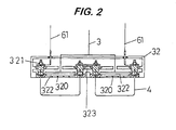
Fig. 2 is a cross-sectional schematic view of a material gas supplying device used for the heating element CVD system ofFig.1 . -
Fig. 3(a) is a partially omitted view of the inside of a processing chamber in a heating element CVD system of the present invention viewed from above, andFig. 3(b) is a perspective view of the side surface of a heating jig. - Hereinafter, with reference to the accompanied drawings, preferable embodiments of the present invention will be explained. However, the configuration, the shaped and the arrangement relationships are shown schematically to the degree that the present invention can be understood, and furthermore, the numerical values and the compositions (materials) of the configurations are merely examples. Therefore, the present invention is not limited to the embodiments explained below, and it can be modified in various forms within the technological scope grasped from the claims.
-
Fig. 1 is a front cross-sectional schematic view for explaining the configuration of a heating element CVD system of the present invention. - The heating element CVD system shown in
Fig. 1 provides a processing chamber 1. A predetermined process, such as the thin film formation on asubstrate 9, and cleaning, is carried out inside the processing chamber 1. The processing chamber 1 provides anevacuating system 2 for evacuating the inside of the processing chamber 1 to a predetermined pressure. Moreover, the processing chamber 1 is connected with agas supplying system 3 for supplying a predetermined material gas (such as a silane (SiH4) gas and a hydrogen (H2) gas in the case of producing a silicon film) into the processing chamber 1. Aheating element 4 is provided in the processing chamber 1 such that the supplied material gas passes by the surface. Theheating element 4 is connected with an electricpower supplying mechanism 6 for giving an energy for maintaining theheating element 4 at a predetermined high temperature (such as 1,600°C to 2,500°C). Thesubstrate 9 is held by asubstrate holder 5 at a predetermined position in the processing chamber 1. The material gas supplied into the processing chamber 1 as the before described is decomposed and/or activated by theheating element 4 maintained at the predetermined high temperature so that a predetermined thin film is produced on thesubstrate 9. Thesubstrate holder 5 can be moved in the vertical direction by an unshown driving system. - Moreover, the
substrate 9 and thesubstrate holder 5 are contacted closely by an unshown electrostatic chucking mechanism. At the time of forming a silicon film, thesubstrate 9 is heated at 300 to 350°C. - As shown in
Fig. 1 , theheating element 4 is held by a materialgas supplying device 32. The materialgas supplying device 32 is connected with thegas supplying system 3 such that a material gas is introduced into the processing chamber 1 via the materialgas supplying device 32 so as to pass by theheating element 4 maintained at a predetermined high temperature. - The processing chamber 1 is an airtight vacuum chamber, providing an unshown gate valve for placing or removing the
substrate 9. - The processing chamber 1 provides an evacuating
opening 11 such that the inside of the processing chamber 1 can be evacuated through the evacuatingopening 11. - The evacuating
system 2 provides avacuum pump 21 such as a turbo molecular pump. The evacuatingsystem 2 connected with the evacuatingopening 11 of the processing chamber 1 is provided so as to evacuate the inside of the processing chamber 1 to about 10-5 to 10-7 Pa. The evacuatingsystem 2 provides an evacuationspeed adjusting device 22 such as a variable orifice. - The
gas supplying system 3 is composed of a gas bomb 31a storing a silane (SiH4) as the material gas, a gas bomb 31b storing a hydrogen (H2) to be mixed with the silane (SiH4), apipe 33 connecting the gas bombs 31a, 31b and the materialgas supplying device 32, avalve 34 and a flowrate adjusting device 35 provided on thepipe 33. - That is, the silane (SiH4) and the hydrogen (H2) from the gas bombs 31a, 31b are mixed halfway in the
pipe 33 become the material gas so as to be introduced into the materialgas supplying device 32. The material gas is blown from agas blowing hole 320 of the materialgas supplying device 32 toward theheating element 4 so as to be supplied into the processing chamber 1. - The
heating element 4 is made of a high melting point metal, such as a tungsten, a molybdenum, and a tantalum. Moreover, the electricpower supplying system 6 is composed so as to energize theheating element 4 for generate the Joule's heat in theheating element 4. That is, the electricpower supplying mechanism 6 is composed so as to maintain theheating element 4 at a predetermined high temperature, for example about 1,600°C to 2,500°C by supplying the electric power. - In
Fig. 1 , the member shown by thenumeral 8 is a structure (heating jig) providing a heating mechanism in itself, for surrounding the space between thesubstrate holder 5 and theheating element 4, which is characteristic of the heating element CVD system of the embodiment of the present invention. - As shown in
Fig. 1 , theheating jig 8 is disposed so as to surround the space between thesubstrate holder 5 and theheating element 4 on the inner side of the inner wall of the processing chamber 1. The inner wall of theheating jig 8 is heated and maintained at least 200°C or higher, preferably at least 350°C or higher by the heating mechanism stored in theheating jig 8. -
Fig. 2 is a cross-sectional schematic view of the materialgas supplying device 32 with theheating element 4 held. The materialgas supplying device 32 is composed of connectingterminals 321 connected with awiring 61 for holding theheating element 4, interlocked with the electricpower supplying mechanism 6 for supplying the electric power to theheating element 4, an interlockingplate 323 for connecting the connectingterminals 321, and materialgas supplying chambers 322 connected with the materialgas supplying system 3 for supplying the supplied material gas from thegas blowing hole 320 into the processing chamber 1 passing through theheating element 4. - Since the construction in which the connecting
terminals 321 and the interlockingplate 323 are not contacted with the material gas is adopted, there is no risk of corrosion, deterioration, or the like. - Since the
heating element 4 is fixed on the connectingterminals 321 fixed on the inside of the materialgas supplying device 32 by a pressuring spring (not shown) or the like, it can be detached easily. Moreover, the distance between thesubstrate 9 and theheating element 4 can be adjusted and/or the distance between theheating elements 4 mounted on the materialgas supplying device 32 can be adjusted according to the size of thesubstrate 9 held by thesubstrate holder 5, the process condition, or the like. -
Fig. 3(a) is a partially omitted view of the inside of the processing chamber 1 of an embodiment of a heating element CVD system characteristic of the present invention, viewed from above (from the materialgas supplying device 32 side) to thesubstrate holder 5 side. In order to explain the installation position of theheating jig 8 for surrounding the space between thesubstrate holder 5 and theheating element 4, the positional relationship of theheating jig 8 is shown with respect to thesubstrate 9 held by thesubstrate holder 5.Fig. 3(b) is a perspective view of the side surface of aheating jig 8. - In
Fig. 3(a) , thesubstrate 9 held on the substrate holder (not shown) is disposed on the center of the processing chamber 1, with the outer circumference thereof surrounded by theheating jig 8 storing theheater 13. - The embodiment is advantageous for effectively heating the space between the
substrate holder 5 and theheating element 4. - The method for fixing the processing chamber 1 and the
heating jig 8 is not limited to the embodiment of being fixed on the upper surface of the processing chamber 1 (shown inFig. 1 ), and a structure without hindering the conveyance of thesubstrate 9 to thesubstrate holder 5, such as an embodiment of being supported on the lower surface of the processing chamber 1 (connecting surface of the evacuating opening 11) by a fixing bracket can be adopted as well. - In
Fig. 3(b) , thenumeral 7 denotes aheating mechanism 7 for heating and maintaining the inner wall ofheating jig 8 at a predetermined temperature. Theheating mechanism 7 is composed of aheater 13 stored in theheating jig 8, asensor 14 for detecting the temperature of theheating jig 8, a heatingtemperature adjusting device 15 for adjusting the input electric power to theheater 13 based on a signal from thesensor 14, awiring 16 for connecting theheater 13, thesensor 14 and the heatingtemperature adjusting device 15, and a connectingpart 12 provided on theheating jig 8 for thewiring 16. - Moreover, in
Fig.3(b) , although theheater 13 is wound spirally for even heating and temperature adjustment, the arrangement of theheater 13 in theheating jig 8 is not limited thereto. Furthermore, inFig.3(b) , although theheater 13 is stored in theheating jig 8 for preventing corrosion or deterioration by the contact with the material gas (silane, hydrogen), theheater 13 can be arranged optionally as long as the heating and temperature adjustment can be carried out so as to maintain the inner wall of theheating jig 8 at least 200°C or higher, or at least 350°C or higher and corrosion and deterioration of theheater 13 is prevented. - The embodiment of the heating element CVD system of the present invention is not limited as the before described.
- For example, although it is not shown, an embodiment having the structure surrounding the space between the
substrate holder 5 and theheating element 4 is the inner wall of the processing chamber 1 such that a heating of the inner surface of the structure is carried out by a heating mechanism stored in the inner wall of the processing chamber 1 thereby the inner wall of the processing chamber 1 can be heated and maintained at least 200°C or higher, preferably at least 350°C or higher can be adopted as well. - Next, the operation of the system of an embodiment shown in
Figs. 1 to 3(b) will be explained together with the explanation for the CVD method of the present invention. - The inside of the preliminary vacuum chamber(not shown) and the processing chamber 1 is evacuated to a predetermined pressure with the
substrate 9 disposed in a preliminary vacuum chamber. With a gate valve (not shown) opened, thesubstrate 9 is conveyed into the processing chamber 1 by an unshown conveying mechanism. According to an unshown driving system, thesubstrate holder 5 is moved vertically so that thesubstrate 9 is placed and held on thesubstrate holder 5. - At the time, the
substrate holder 5 is maintained at a predetermined temperature (for example, 300 to 350°C), and thesubstrate 9 and thesubstrate holder 5 are contacted closely by the electrostatic chuck (not shown). - Next, the electric
power supplying mechanism 6 starts to energize theheating element 4 so as to maintain theheating element 4 at a predetermined high temperature. Moreover, theheater 13 stored in theheating jig 8 is energized so as to operate the heatingtemperature adjusting device 15 for heating the heater13 to a predetermined temperature, for example 350°C. In the case theheating element 4 is maintained at a predetermined temperature, and the inner surface temperature of theheating jig 8 is confirmed to have reached at 350°C by thesensor 14, thegas supplying system 3 is operated so that the material gas, that is, a silane gas mixed with a hydrogen gas is introduced into the processing chamber 1 while adjusting the flow rate by the flowrate adjusting device 35. Thereafter, the inside of the processing chamber 1 is maintained at a predetermined pressure by the evacuatingsystem 2. - The electric power supply amount of the
heater 13 is adjusted such that the inner surface of theheating jig 8 is maintained at least 350°C or higher in the case the heating element CVD system of the present invention is used in a several tens Pa pressure area, and the inner surface of theheating jig 8 is heated and maintained at least 200°C or higher in the case the heating element CVD system of the present invention is used in a relatively low pressure range, for example, of a several Pa pressure area. - Since it takes a long time for heating to 350°C or higher, the production efficiency can be improved by adjusting the temperature to 200°C or higher even in the case the film forming is not executed for shortening the heating time to 350°C or higher.
- As a result, the material gas decomposed and/or activated on the surface of the
heating element 4 can efficiently reach the surface of thesubstrate 9 so that a polycrystalline silicon film can be deposited on the surface of thesubstrate 9. - After passage of a time needed for having the thin film thickness reaching at a predetermined thickness, the
valve 34 of thegas supplying system 3 is closed as well as the operation of the electricpower supplying mechanism 6 is stopped. As needed, the electric power supply to theheating element 4 and theheater 13 may be blocked. - After operating the evacuating
system 2 so as to evacuate the inside of the processing chamber 1 again to the predetermined pressure, the unshown gate valve is opened for taking out thesubstrate 9 from the processing chamber 1 by the unshown conveying mechanism. Thereby, a series of the film forming process can be finished. - An example of the film forming condition for forming a silicon film (film thickness: 1,000 nm) by a CVD method of the present invention using a heating element CVD system of the present invention will be shown below. In this example, a
heating jig 8 surrounding the space between thesubstrate holder 5 and theheating element 4 on the inner side of the processing chamber 1 as in the embodiment shown inFig. 1 is used as the structure surrounding the space between thesubstrate holder 5 and theheating element 4.Substrate φ8 Si substrate Pressure in the processing chamber 1 2 Pa SiH4 flow rate 3 ml/min H2 flow rate 100 ml/min Temperature of the heating element 41,800°C Temperature of the inner surface of the heating jig 8350°C Distance between the heating element 4 and thesubstrate 945 mm - In contrast, a silicon film (film thickness: 1,000 nm) was formed in the same condition except that the heating operation by the
heating jig 8 was not carried out, using the same heating element CVD system, and it was provided as a comparative example. - The electron mobility was measured for the both silicon films (film thickness: 1,000 nm).
- As a result, it was confirmed that the electron mobility of the silicon film of the comparative example was at most 1 cm2/Vs, which is substantially same as an amorphous film, but the electron mobility was improved according to the silicon film formed with the inner surface of the
heating jig 8 maintained at 350°C using the system and the method of the present invention. - The other heating element CVD system of the present invention is used, in which the inner wall of the processing chamber 1 is used as the structure surrounding the space between the
substrate holder 5 and theheating element 4. A silicon film(film thickness:1,000nm)was formed in the same condition as the before described using this heating element CVD system with the inner surface of the wall of processing chamber 1 maintained at 350°C. The electron mobility was measured for this silicon film. And, it was also confirmed that the electron mobility of this silicon film was improved. - Although preferable embodiments in the polycrystalline silicon film formation have been described in the above-mentioned examples, the configuration of the heating element CVD system and the heating element CVD method disclosed in the present invention are essential in stably forming of high quality thin film. Therefore, the heating element CVD system and the heating element CVD method using the same of the present invention can be adopted for formation of the kinds of films with the atomic hydrogen produced during the film formation, such as a silicon carbide film obtained using the material gas comprising at least one selected from the group consisting of a methane (CH4), an acetylene (C2H2) and an ethane (C2H6), and a silane (SiH4) and a hydrogen (H2), a silicon germanium film obtained using the material gas comprising a silane (SiH4), a germane (GeH4) and a hydrogen (H2), or the like.
Claims (1)
- A CVD system comprising:a processing chamber (1);a substrate holder (5) in said processing chamber;an evacuating system (2) configured to evacuate said processing chamber, said evacuating system connected to said processing chamber;a material gas supplying chamber (32) enclosing the electric power supply unit (321) therein; and having a gas blowing face provided with a plurality of holes (320), said material gas supplying device configured to supply a material gas into said processing chamber through the holes; anda heating element (4) configured to be heated by electric power supplied from the electric power supply unit in said processing chamber, for heating the material gas supplied into the processing chamber from the holes to decompose and/or activate the material gas supplied into the processing chamber from the holes;wherein the material gas supplying chamber contains therein two power supply terminals disposed respectively at both lateral sides aside the gas blowing face, for detachably holding said heating element to extend in front of the gas blowing face and between the power supply terminals, for an electrical connection of the heating element to the electric power supply unit, andwherein power supply terminals enclosed inside the material gas supplying chamber are located in a space partitioned from the processing chamber to be prevented from contacting the material gas supplied into the processing chamber from the holes.
Applications Claiming Priority (2)
| Application Number | Priority Date | Filing Date | Title |
|---|---|---|---|
| JP2001349075 | 2001-11-14 | ||
| EP02257886A EP1312698A1 (en) | 2001-11-14 | 2002-11-14 | Heating element CVD System and heating element CVD method using the same |
Related Parent Applications (1)
| Application Number | Title | Priority Date | Filing Date |
|---|---|---|---|
| EP02257886.8 Division | 2002-11-14 |
Publications (1)
| Publication Number | Publication Date |
|---|---|
| EP2208806A1 true EP2208806A1 (en) | 2010-07-21 |
Family
ID=19161799
Family Applications (2)
| Application Number | Title | Priority Date | Filing Date |
|---|---|---|---|
| EP02257886A Withdrawn EP1312698A1 (en) | 2001-11-14 | 2002-11-14 | Heating element CVD System and heating element CVD method using the same |
| EP10003577A Withdrawn EP2208806A1 (en) | 2001-11-14 | 2002-11-14 | Heating element CVD system |
Family Applications Before (1)
| Application Number | Title | Priority Date | Filing Date |
|---|---|---|---|
| EP02257886A Withdrawn EP1312698A1 (en) | 2001-11-14 | 2002-11-14 | Heating element CVD System and heating element CVD method using the same |
Country Status (5)
| Country | Link |
|---|---|
| US (1) | US20060254516A1 (en) |
| EP (2) | EP1312698A1 (en) |
| KR (2) | KR20030040119A (en) |
| CN (1) | CN1276472C (en) |
| TW (1) | TWI245329B (en) |
Families Citing this family (7)
| Publication number | Priority date | Publication date | Assignee | Title |
|---|---|---|---|---|
| JP4157718B2 (en) | 2002-04-22 | 2008-10-01 | キヤノンアネルバ株式会社 | Silicon nitride film manufacturing method and silicon nitride film manufacturing apparatus |
| JP3787816B2 (en) * | 2002-10-04 | 2006-06-21 | キヤノンアネルバ株式会社 | Heating element CVD equipment |
| US7422983B2 (en) * | 2005-02-24 | 2008-09-09 | International Business Machines Corporation | Ta-TaN selective removal process for integrated device fabrication |
| CN100466164C (en) * | 2005-12-08 | 2009-03-04 | 北京圆合电子技术有限责任公司 | A gas filling system for a vacuum chamber |
| JP4948021B2 (en) * | 2006-04-13 | 2012-06-06 | 株式会社アルバック | Catalytic chemical vapor deposition system |
| WO2009049477A1 (en) * | 2007-09-20 | 2009-04-23 | Changzhou Ennoah Energy Technology Corporation Ltd. | Process and apparatus for producing polysilicon sheets |
| AT519217B1 (en) * | 2016-10-04 | 2018-08-15 | Carboncompetence Gmbh | Apparatus and method for applying a carbon layer |
Citations (2)
| Publication number | Priority date | Publication date | Assignee | Title |
|---|---|---|---|---|
| JPH03239320A (en) * | 1990-02-16 | 1991-10-24 | Fuji Electric Co Ltd | Catalyst cvd apparatus |
| WO2002025712A1 (en) * | 2000-09-14 | 2002-03-28 | Japan As Represented By President Of Japan Advanced Institute Of Science And Technology | Heating element cvd device |
Family Cites Families (27)
| Publication number | Priority date | Publication date | Assignee | Title |
|---|---|---|---|---|
| US3373198A (en) * | 1967-04-27 | 1968-03-12 | American Cyanamid Co | Substituted 5a, 11a-dehydro-6-epitetracyclines |
| JPS59207620A (en) * | 1983-05-10 | 1984-11-24 | Zenko Hirose | Amorphous silicon film forming apparatus |
| DE3539981C1 (en) * | 1985-11-11 | 1987-06-11 | Telog Systems Gmbh | Method and device for treating semiconductor materials |
| US5594280A (en) * | 1987-10-08 | 1997-01-14 | Anelva Corporation | Method of forming a thin film and apparatus of forming a metal thin film utilizing temperature controlling means |
| US5128515A (en) * | 1990-05-21 | 1992-07-07 | Tokyo Electron Sagami Limited | Heating apparatus |
| WO1992016671A1 (en) * | 1991-03-20 | 1992-10-01 | Canon Kabushiki Kaisha | Method and device for forming film by sputtering process |
| JP2532401Y2 (en) * | 1991-04-16 | 1997-04-16 | ソニー株式会社 | Bias ECR plasma CVD equipment |
| JPH05243167A (en) * | 1992-02-28 | 1993-09-21 | Sony Corp | Manufacture of semiconductor device |
| US5383984A (en) * | 1992-06-17 | 1995-01-24 | Tokyo Electron Limited | Plasma processing apparatus etching tunnel-type |
| JP3165938B2 (en) * | 1993-06-24 | 2001-05-14 | 東京エレクトロン株式会社 | Gas treatment equipment |
| US5522933A (en) * | 1994-05-19 | 1996-06-04 | Geller; Anthony S. | Particle-free microchip processing |
| JPH088194A (en) * | 1994-06-16 | 1996-01-12 | Kishimoto Sangyo Kk | Heating device in vapor phase growth mechanism and heat treatment mechanism |
| US5735960A (en) * | 1996-04-02 | 1998-04-07 | Micron Technology, Inc. | Apparatus and method to increase gas residence time in a reactor |
| US5788799A (en) * | 1996-06-11 | 1998-08-04 | Applied Materials, Inc. | Apparatus and method for cleaning of semiconductor process chamber surfaces |
| JPH10134996A (en) * | 1996-10-31 | 1998-05-22 | Nec Corp | Plasma treatment equipment |
| US6055927A (en) * | 1997-01-14 | 2000-05-02 | Applied Komatsu Technology, Inc. | Apparatus and method for white powder reduction in silicon nitride deposition using remote plasma source cleaning technology |
| US5993679A (en) * | 1997-11-06 | 1999-11-30 | Anelva Corporation | Method of cleaning metallic films built up within thin film deposition apparatus |
| JP3132489B2 (en) * | 1998-11-05 | 2001-02-05 | 日本電気株式会社 | Chemical vapor deposition apparatus and thin film deposition method |
| WO2000063956A1 (en) * | 1999-04-20 | 2000-10-26 | Sony Corporation | Method and apparatus for thin-film deposition, and method of manufacturing thin-film semiconductor device |
| KR100302609B1 (en) * | 1999-05-10 | 2001-09-13 | 김영환 | Temperature controllable gas distributor |
| US6227140B1 (en) * | 1999-09-23 | 2001-05-08 | Lam Research Corporation | Semiconductor processing equipment having radiant heated ceramic liner |
| JP2001152338A (en) * | 1999-11-29 | 2001-06-05 | Japan Science & Technology Corp | High conductivity diamond-like carbon thin film production equipment |
| JP2001210594A (en) * | 2000-01-26 | 2001-08-03 | Matsushita Electric Ind Co Ltd | Thin film deposition apparatus and thin film deposition method |
| JP4522527B2 (en) * | 2000-03-06 | 2010-08-11 | キヤノンアネルバ株式会社 | Substrate mounting method in semiconductor manufacturing equipment |
| KR100507753B1 (en) * | 2000-03-17 | 2005-08-10 | 가부시키가이샤 히타치세이사쿠쇼 | Method of manufacturing semiconductor and manufacturing apparatus |
| US20020011205A1 (en) * | 2000-05-02 | 2002-01-31 | Shunpei Yamazaki | Film-forming apparatus, method of cleaning the same, and method of manufacturing a light-emitting device |
| US6461435B1 (en) * | 2000-06-22 | 2002-10-08 | Applied Materials, Inc. | Showerhead with reduced contact area |
-
2002
- 2002-11-13 KR KR1020020070237A patent/KR20030040119A/en not_active Ceased
- 2002-11-13 TW TW091133289A patent/TWI245329B/en not_active IP Right Cessation
- 2002-11-14 CN CNB021504814A patent/CN1276472C/en not_active Expired - Fee Related
- 2002-11-14 EP EP02257886A patent/EP1312698A1/en not_active Withdrawn
- 2002-11-14 EP EP10003577A patent/EP2208806A1/en not_active Withdrawn
-
2006
- 2006-07-20 US US11/489,522 patent/US20060254516A1/en not_active Abandoned
-
2010
- 2010-02-23 KR KR1020100016125A patent/KR100972962B1/en not_active Expired - Fee Related
Patent Citations (3)
| Publication number | Priority date | Publication date | Assignee | Title |
|---|---|---|---|---|
| JPH03239320A (en) * | 1990-02-16 | 1991-10-24 | Fuji Electric Co Ltd | Catalyst cvd apparatus |
| WO2002025712A1 (en) * | 2000-09-14 | 2002-03-28 | Japan As Represented By President Of Japan Advanced Institute Of Science And Technology | Heating element cvd device |
| EP1258914A1 (en) * | 2000-09-14 | 2002-11-20 | Japan as represented by President of Japan Advanced Institute of Science and Technology | Heating element cvd device |
Also Published As
| Publication number | Publication date |
|---|---|
| KR100972962B1 (en) | 2010-07-30 |
| KR20030040119A (en) | 2003-05-22 |
| EP1312698A1 (en) | 2003-05-21 |
| CN1419268A (en) | 2003-05-21 |
| US20060254516A1 (en) | 2006-11-16 |
| TWI245329B (en) | 2005-12-11 |
| CN1276472C (en) | 2006-09-20 |
| KR20100037071A (en) | 2010-04-08 |
| TW200300271A (en) | 2003-05-16 |
Similar Documents
| Publication | Publication Date | Title |
|---|---|---|
| US20210010160A1 (en) | Method and apparatus for precleaning a substrate surface prior to epitaxial growth | |
| US6656282B2 (en) | Atomic layer deposition apparatus and process using remote plasma | |
| US6755151B2 (en) | Hot-filament chemical vapor deposition chamber and process with multiple gas inlets | |
| US20090277386A1 (en) | Catalytic chemical vapor deposition apparatus | |
| EP1258914B1 (en) | Heating element cvd device | |
| KR101976559B1 (en) | Methods for cleaning a surface of a substrate using a hot wire chemical vapor deposition (hwcvd) chamber | |
| US8071477B2 (en) | Method of manufacturing semiconductor device and substrate processing apparatus | |
| WO2019103995A1 (en) | Methods of reducing or eliminating defects in tungsten film | |
| JP2566914B2 (en) | Thin film semiconductor device and method of forming the same | |
| US7211152B2 (en) | Heating element CVD system and connection structure between heating element and electric power supply mechanism in the heating element CVD system | |
| KR100972962B1 (en) | Heating element cvd apparatus | |
| JPH1154441A (en) | Catalytic chemical vapor deposition equipment | |
| US20030131795A1 (en) | Heating element CVD system and heating element CVD method using the same | |
| US20070105373A1 (en) | Method of direct deposition of polycrystalline silicon | |
| EP0240306A1 (en) | Method for forming deposited film | |
| EP0240314B1 (en) | Method for forming deposited film | |
| JP4221489B2 (en) | Heating element CVD apparatus and heating element CVD method using the same | |
| RU2769751C1 (en) | Device for deposition of ultra-thick layers of polycrystalline silicon | |
| JP3887690B2 (en) | Connection structure between heating element and power supply mechanism in heating element CVD device | |
| Rondiya et al. | Physical Methods for Synthesis and Thin-Film Deposition | |
| JP2006319306A (en) | In situ growth method for polycrystalline thin films. | |
| JPH08100264A (en) | Formation of thin film and device therefor | |
| EP2485248B1 (en) | Film forming method using catalytic cvd device | |
| JP4093238B2 (en) | Thin film formation method | |
| JPH11260726A (en) | Manufacture of single crystalline silicon thin film and polycrystalline silicon thin film |
Legal Events
| Date | Code | Title | Description |
|---|---|---|---|
| PUAI | Public reference made under article 153(3) epc to a published international application that has entered the european phase |
Free format text: ORIGINAL CODE: 0009012 |
|
| 17P | Request for examination filed |
Effective date: 20100331 |
|
| AC | Divisional application: reference to earlier application |
Ref document number: 1312698 Country of ref document: EP Kind code of ref document: P |
|
| AK | Designated contracting states |
Kind code of ref document: A1 Designated state(s): DE ES FR GB NL PT |
|
| STAA | Information on the status of an ep patent application or granted ep patent |
Free format text: STATUS: THE APPLICATION IS DEEMED TO BE WITHDRAWN |
|
| 18D | Application deemed to be withdrawn |
Effective date: 20110122 |