EP2204856A1 - Light emitting diode drive device, illumination device, in-vehicle cabin illumination device, and vehicle illumination device - Google Patents
Light emitting diode drive device, illumination device, in-vehicle cabin illumination device, and vehicle illumination device Download PDFInfo
- Publication number
- EP2204856A1 EP2204856A1 EP08841637A EP08841637A EP2204856A1 EP 2204856 A1 EP2204856 A1 EP 2204856A1 EP 08841637 A EP08841637 A EP 08841637A EP 08841637 A EP08841637 A EP 08841637A EP 2204856 A1 EP2204856 A1 EP 2204856A1
- Authority
- EP
- European Patent Office
- Prior art keywords
- light emitting
- circuit section
- emitting diode
- voltage
- drive device
- Prior art date
- Legal status (The legal status is an assumption and is not a legal conclusion. Google has not performed a legal analysis and makes no representation as to the accuracy of the status listed.)
- Granted
Links
Images


Classifications
-
- H—ELECTRICITY
- H05—ELECTRIC TECHNIQUES NOT OTHERWISE PROVIDED FOR
- H05B—ELECTRIC HEATING; ELECTRIC LIGHT SOURCES NOT OTHERWISE PROVIDED FOR; CIRCUIT ARRANGEMENTS FOR ELECTRIC LIGHT SOURCES, IN GENERAL
- H05B45/00—Circuit arrangements for operating light-emitting diodes [LED]
- H05B45/50—Circuit arrangements for operating light-emitting diodes [LED] responsive to malfunctions or undesirable behaviour of LEDs; responsive to LED life; Protective circuits
- H05B45/58—Circuit arrangements for operating light-emitting diodes [LED] responsive to malfunctions or undesirable behaviour of LEDs; responsive to LED life; Protective circuits involving end of life detection of LEDs
-
- H—ELECTRICITY
- H05—ELECTRIC TECHNIQUES NOT OTHERWISE PROVIDED FOR
- H05B—ELECTRIC HEATING; ELECTRIC LIGHT SOURCES NOT OTHERWISE PROVIDED FOR; CIRCUIT ARRANGEMENTS FOR ELECTRIC LIGHT SOURCES, IN GENERAL
- H05B45/00—Circuit arrangements for operating light-emitting diodes [LED]
- H05B45/10—Controlling the intensity of the light
-
- H—ELECTRICITY
- H05—ELECTRIC TECHNIQUES NOT OTHERWISE PROVIDED FOR
- H05B—ELECTRIC HEATING; ELECTRIC LIGHT SOURCES NOT OTHERWISE PROVIDED FOR; CIRCUIT ARRANGEMENTS FOR ELECTRIC LIGHT SOURCES, IN GENERAL
- H05B45/00—Circuit arrangements for operating light-emitting diodes [LED]
- H05B45/30—Driver circuits
- H05B45/37—Converter circuits
- H05B45/3725—Switched mode power supply [SMPS]
- H05B45/38—Switched mode power supply [SMPS] using boost topology
-
- H—ELECTRICITY
- H05—ELECTRIC TECHNIQUES NOT OTHERWISE PROVIDED FOR
- H05B—ELECTRIC HEATING; ELECTRIC LIGHT SOURCES NOT OTHERWISE PROVIDED FOR; CIRCUIT ARRANGEMENTS FOR ELECTRIC LIGHT SOURCES, IN GENERAL
- H05B45/00—Circuit arrangements for operating light-emitting diodes [LED]
- H05B45/30—Driver circuits
- H05B45/37—Converter circuits
- H05B45/3725—Switched mode power supply [SMPS]
- H05B45/385—Switched mode power supply [SMPS] using flyback topology
Definitions
- the present invention relates to a light emitting diode drive device, as well as an illumination device, an in-vehicle cabin illumination device and a vehicle illumination device each employing the light emitting diode drive device.
- a light emitting diode As compared with an incandescent bulb, a light emitting diode is long in service life and excellent in responsivity of light emission upon reception of electric power because of light emission principles thereof. Moreover, a light emitting diode can be used in a compact and stereoscopic manner, and therefore is less susceptible to restrictions regarding a shape as an illumination device. Further, a light emitting diode can readily realize light emission of various colors without filters or the like. Accordingly, there have been proposed various illumination devices each including such a light emitting diode serving as a light source and various light emitting diode drive devices for supplying electric power to the light emitting diode.
- a white light emitting diode has been put into practical use, and therefore uses of an illumination device including such a light emitting diode serving as a light source have been increased.
- a white light emitting diode is used for vehicle illumination devices such as an in-vehicle cabin illuminator, a headlight, an auxiliary lamp and a daytime running lamp.
- a light emitting diode drive device for supplying electric power to a light emitting diode includes a drive circuit section that applies a predetermined direct-current voltage to a light source including a plurality of light emitting diodes connected in series in order to secure a quantity of light and allows the light source to light up.
- Examples of such a light emitting diode drive device include a device that controls a drive circuit section in a PWM manner in order to stably supply desired electric current or electric power to a light source, and a device that detects an electrical abnormality of a light emitting diode (e.g., refer to Patent Document 1, Patent Document 2).
- a light emitting diode drive device that allows light emission from a light source including a plurality of light emitting diodes connected in series, it is desirable to detect a short circuit of the light emitting diode which lights up.
- a light emitting diode drive device having the following structure. That is, a drive circuit section 3 receives electric power from a power supply 8, converts the electric power into a predetermined direct-current voltage, and applies the direct-current voltage to a light source 2.
- the light source 2 includes a plurality of light emitting diodes 1, and a plurality of voltage detection circuit sections 4' each detect a voltage across the relevant light emitting diode 1.
- An abnormality detection circuit section 5' detects an abnormality of each light emitting diode 1, based on the voltage detected by the voltage detection circuit section 4'.
- a light emitting diode drive device having the following structure. That is, a plurality of light emitting diodes are divided into several sets, and an abnormality detection circuit section detects a voltage across each set.
- the light emitting diode drive device including the abnormality detection circuit section described above can widely detect electrical abnormalities such as a short circuit and a break of the light emitting diode.
- the light emitting diode drive device needs to detect the voltage at each of the plurality of light emitting diodes. Consequently, the light emitting diode drive device requires the voltage detection circuit sections 4' which are equal in number to the plurality of light emitting diodes. This structure complicates a circuit configuration.
- the present invention has been devised in view of the circumstances described above, and one object thereof is to provide a light emitting diode drive device for applying a direct-current voltage to a light source including a plurality of light emitting diodes connected in series to allow the light source to light up.
- This light emitting diode drive device can determine whether or not the light emitting diode, which lights up, is short-circuited with a simple circuit configuration as compared with a conventional light emitting diode drive device having circuitry for detecting voltages at a plurality of light emitting diodes.
- this light emitting diode drive device can be manufactured with smaller manufacturing steps at lower manufacturing cost as compared with a conventional light emitting diode drive device including a plurality of voltage detection circuit sections.
- Another object of the present invention is to provide an illumination device, an in-vehicle cabin illumination device and a vehicle illumination device each employing the light emitting diode drive device.
- the following embodiments will exemplify a light emitting diode drive device for use in a headlight of a vehicle.
- the light emitting diode drive device A includes a drive circuit section 3 that converts electric power supplied from a power supply 8 into a direct-current voltage and outputs the direct-current voltage, a voltage detection circuit section 4 that detects a voltage across a light source 2 including a plurality of light emitting diodes 1 connected in series, a malfunction determination circuit section 5 that determines whether or not the light emitting diode 1, which lights up, is short-circuited, based on the voltage detected by the voltage detection circuit section 4, a display section 6 that displays the result of determination by the malfunction determination circuit section 5, and a current detection circuit section 7 that detects an electric current to be fed to the light source 2.
- the power supply 8 for supplying electric power to the light emitting diode drive device A is a battery that outputs a direct-current voltage.
- the power supply 8 has an output terminal connected with an input side of the drive circuit section 3.
- the drive circuit section 3 boosts the direct-current voltage output from the power supply 8, and outputs the boosted direct-current voltage through an output side thereof.
- the light source 2 is connected to the output side of the drive circuit section 3 and receives the boosted direct-current voltage, so that the plurality of light emitting diodes 1, which form the light source 2, each emit light.
- the voltage detection circuit section 4 includes voltage detection resistors 4a and 4b connected in series between two terminals of the light source 2.
- the voltage detection resistors 4a and 4b each divide the voltage across the light source 2 and output the divided voltage. This divided voltage is proportional to the voltage across the light source 2, and therefore allows detection of the voltage across the light source 2.
- the current detection circuit section 7 includes a current detection resistor 7a. The current detection resistor 7a outputs a voltage drop at the current detection resistor 7a in a form of signal voltage. This signal voltage is proportional to an electric current flowing through the light source 2, and therefore allows detection of the electric current flowing through the light source 2.
- the malfunction determination circuit section 5 determines whether or not the light emitting diode 1, which lights up, is short-circuited, based on the detected divided voltage.
- the display section 6 displays the fact that the light emitting diode 1 is short-circuited or is not short-circuited, which is determined by the malfunction determination circuit section 5.
- Fig. 2 shows a simplified portion regarding PWM control.
- the drive circuit section 3 is a booster converter 3a which is a step-up type switching power supply circuit.
- the booster converter 3a serving as the drive circuit section 3 boosts a direct-current voltage from the power supply 8 to output a required voltage, and then supplies the voltage to the light source 2.
- the booster converter 3a includes an inductor 9 having a first end connected to a high-voltage side of the power supply 8, a backflow prevention diode 10 having an anode connected to a second end of the inductor 9, a capacitor 11 connected between a cathode side of the diode 10 and a low-voltage side of the power supply 8, and a switch element 12 connected between the anode side of the diode 10 and the low-voltage side of the power supply 8.
- the switch element 12 may include a power MOSFET (Metal Oxide Semiconductor Field Effect Transistor) and the like.
- the capacitor 11 is electrically charged when the switch element 12 is turned off while the inductor 9 receives electric current when the switch element 12 is turned on.
- the electric current flowing through the inductor 9 increases because of self induction as a time elapses.
- the switch element 12 is turned off again, no electric current flows through the inductor 9 and a magnetic flux formed by the electric current in the inductor 9 decreases, so that there occurs a change in magnetic flux. Accordingly, an inverted electromotive force is generated in a direction that the change in magnetic force is prevented, that is, a direction that an electric current is continuously fed to the inductor 9.
- the voltage across the capacitor 11 (the output voltage) is generated in such a manner that a voltage based on the inverted electromotive force generated in the inductor 9 is superimposed on a voltage based on the electrical charge in the capacitor 11 in the state in which the switch element 12 is turned off.
- the resultant voltage is equal to or more than the voltage at the power supply 8.
- the switch element 12 is turned on and off periodically to boost the voltage.
- the magnitude of the inverted electromotive force generated at the inductor 9 depends on the magnitude of the formed magnetic flux, and therefore the inverted electromotive force becomes large as the electric current flowing through the inductor 9 is large. Moreover, since the electric current increases as a time elapses, the magnitude of the output direct-current voltage becomes high as the ON period of the switch element 12 is long. A change in ratio between the ON period and the OFF period of the switch element 12 in one cycle allows a change in magnitude of the direct-current voltage to be output from the booster converter 3a.
- duty control control for changing a ratio between an ON period and an OFF period of a switch element in one cycle
- PWM Pulse Width Modulation
- the output from the booster converter 3a is controlled using this PWM control, so that the electric power to be supplied to the light source 2 is set suitable for light emission from the light source 2 and is kept at a certain level.
- the electric power to be supplied to the light source 2 is kept at a certain level, the intensity of light emitted from the light emitting diode 1 becomes stable.
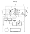
- Fig. 3 shows details of the PWM control which is shown in Fig. 2 in a simplified manner. The PWM control is described with reference to Fig. 3 .
- the booster converter 3a includes a PWM control circuit section 13 and a driver circuit section 18.
- the PWM control circuit section 13 includes a power supply circuit section 14, a reference value generation circuit section 16 and a PWM control signal generation circuit section 17.
- the power supply circuit section 14 receives the electric power from the power supply 8 to generate an operating power supply voltage for the PWM control circuit section 13, and drives the PWM control circuit section 13.
- An amplification circuit section 15 includes a divided voltage amplifier 15a and a signal voltage amplifier 15b.
- the amplification circuit section 15 amplifies a divided voltage to output an amplified divided voltage, and also amplifies a signal voltage to output an amplified signal voltage.
- the amplified divided voltage is input to the reference value generation circuit section 16 through the PWM control signal generation circuit section 17.
- the reference value generation circuit section 16 divides a target electric power value set therein by the amplified divided voltage to set a target electric current to be fed to the light source 2, and generates a reference voltage corresponding to the set target electric current.
- the PWM control signal generation circuit section 17 compares the amplified signal voltage with a reference voltage, and generates a PWM control signal corresponding to the difference between the amplified signal voltage and the reference voltage.
- a driver circuit section 18 receives the PWM control signal to output a drive signal for controlling the ON/OFF state of the switch element 12 of the booster converter 3a.
- the booster converter 3a is subjected to the PWM control, based on this drive signal, and the output therefrom is kept at a certain level.
- the malfunction determination circuit section 5 includes a first holding section 19 that holds a divided voltage of the voltage across the light source 2 (herein, the divided voltage is detected by the voltage detection circuit section 4) every predetermined sampling time T, a second holding section 20 that holds the divided voltage held by the first holding section 19 before the first holding section 19 holds a new divided voltage (i.e., a divided voltage acquired at a preceding sampling timing), a time setting circuit section 21 that sets the sampling time T, a differential circuit section 22 that outputs a differential value between the voltage held by the first holding section 19 and the voltage held by the second holding section 20, a threshold value setting circuit section 23 that sets a threshold value for determining whether or not the output from the differential circuit section 22 is adequate to a short circuit of the light emitting diode 1, and a comparison circuit section 24 that compares the output from the differential circuit section 22 with the threshold value to determine whether or not the light emitting diode 1 is short-circuited.
- a first holding section 19 that holds a divided voltage of the voltage across the light source
- a lateral axis indicates a time, in which "t1", “t2", ... and “t6" each represent a timing that the first holding section 19 holds a divided voltage detected by the voltage detection circuit section 4.
- a vertical axis indicates a voltage, in which " ⁇ V” represents a value of drop of the voltage across the light source 2 in a case where one light emitting diode 1 is short-circuited.
- the divided voltage detected by the voltage detection circuit section 4 is held by the first holding section 19 at the timing t3.
- the divided voltage, which is detected at the timing t3 and is held by the first holding section 19 is transferred to the second holding section 20 and is held by the second holding section 20.
- the divided voltage, which is detected at the timing t4 is held by the first holding section 19.
- the differential circuit section 22 outputs a differential value between the divided voltage held by the first holding section 19 and the divided voltage held by the second holding section 20.
- the comparison circuit section 24 compares the threshold value with the output from the differential circuit section 22, and when the output from the differential circuit section 22 is equal to or more than the threshold value, determines that the light emitting diode 1 is short-circuited.
- the threshold value is set with the forward voltage at one light emitting diode 1 used as a reference.
- the change of the voltage across the light source 2 because of the short circuit of the light emitting diode 1 depends on variations in characteristics of the light emitting diodes 1 in the process of manufacture, variations in voltage output from the power supply 8, and a secular change of the light emitting diode 1 caused by an ambient temperature and a light emitting operation. Accordingly, these factors occasionally lower accuracy of determining whether the light emitting diode 1, which lights up, is short-circuited.
- the threshold value can be changed by the threshold value setting circuit section 23.
- the threshold value setting circuit section 23 can change the threshold value, based on an external input signal.
- the light emitting diode drive device A may be provided with a knob for changing the settings, and this knob may be operated for changing the threshold value.
- the length of the sampling time T also exerts an adverse influence on the accuracy of determination about the short circuit, and therefore can be changed by the time setting circuit section 21.
- the time setting circuit section 21 can change the sampling time T, based on an external input signal.
- the light emitting diode drive device A may be provided with a knob for changing the settings, and this knob may be turned for changing the sampling time T.
- the result of determination by the malfunction determination circuit section 5, that is, the fact that the light emitting diode 1 is short-circuited or is not short-circuited is stored in a memory circuit section 40 (see Fig. 1 ) which is a nonvolatile memory circuit, for example.
- the display section 6 receives the result from the memory circuit section 40, and displays the fact that the light emitting diode 1 is short-circuited or is not short-circuited.
- the display section 6 is provided on a panel display section in an operating seat.
- the display section 6 prompts the user to repair the short-circuited light emitting diode 1.
- the PWM control signal generation circuit section 17 determines whether or not the memory circuit section 40 stores therein the fact that the light emitting diode 1 is short-circuited.
- the PWM control signal generation circuit section 17 turns the switch element 12 off, for example.
- the output voltage from the power supply 8 is set at a voltage having a value obtained by multiplying a numeric value which is smaller by one than the number of light emitting diodes 1 in the light source 2 by a value of a forward ON voltage at the light emitting diode 1, that is, a voltage which is lower than a threshold voltage required for allowing the light source 2 to light up in a state in which one of the light emitting diodes 1 is short-circuited.
- the power supply 8 is a battery for outputting a direct-current voltage; however, the present invention is not limited thereto.
- the power supply 8 may include an alternating-current power supply 8a.
- the PWM control signal generation circuit section 17 turns the switch element 12 off to lower the voltage to be applied to the light source 2 to a level below the threshold voltage, so that the light source 2 is turned out.
- the power supply 8 including the alternating-current power supply 8a also includes a rectifying diode 33 that rectifies an alternating current, and a smoothing capacitor 34 that smoothes the electric current rectified by the rectifying diode 33.
- a rectifying diode 33 that rectifies an alternating current
- a smoothing capacitor 34 that smoothes the electric current rectified by the rectifying diode 33.
- two ends of the smoothing capacitor 34 serve as output terminals of the power supply 8.
- a light emitting diode drive device A according to the present embodiment is different from the light emitting diode drive device A according to the first embodiment in a point that a flyback converter 3b including a flyback transformer 28 is provided in place of the drive circuit section 3.
- the remaining configuration is similar to that described in the first embodiment.
- constituent members identical with those in the first embodiment are denoted with the identical reference signs, and therefore the description thereof will not be given.
- the flyback converter 3b includes a flyback transformer 28 that includes a power supply-side wire 26 wound around a core (not shown) with a first end thereof connected to a high pressure side of a power supply 8 which is a direct-current power supply and a output-side wire 27 coupled magnetically to the power supply-side wire 26 and wound around a core (not shown) in a direction opposite to that of the power supply-side wire 26, a flyback switch element 29 connected to a second end of the power supply-side wire 26 and a low pressure side of the power supply 8, a backflow preventing flyback diode 30 having an anode connected to a first end of the output-side wire 27, and a flyback capacitor 31 connected to a cathode of the flyback diode 30 and a second end of the output-side wire 27.
- the flyback switch element 29 may include a power MOSFET and the like.
- the flyback switch element 29 During a period of time that the flyback switch element 29 is turned on, an electric current flows through the power supply-side wire 26.
- the electric current flowing through the power supply-side wire 26 increases because of self induction as a time elapses.
- an electromotive force is generated at the output-side wire 27 because of mutual induction, but is directed inversely since the output-side wire 27 is wound inversely with respect to the power supply-side wire 26. Accordingly, the flyback diode 30 prevents the electric current from flowing through the output-side wire 27.
- the flyback switch element 29 is turned off. When the flyback switch element 29 is turned off, a magnetic flux formed on the power supply-side wire 26 decreases.
- the electromotive force is generated because of the mutual induction at the output-side wire 27.
- This electromotive force serves as an output from the flyback converter 3b.
- the flyback switch element 29 when the flyback switch element 29 is turned on, a magnetic force is accumulated in the power supply-side wire 26.
- the flyback switch element 29 when the flyback switch element 29 is turned off, the magnetic force is released from the output-side wire 27.
- a voltage is generated at the output-side wire 27.
- the electric current flowing through the power supply-side wire 26 increases as the time elapses. For this reason, the magnetic force to be accumulated in the power supply-side wire 26 becomes strong as the ON period of the flyback switch element 29 is long, so that the output voltage becomes high.
- the booster converter 3a it is possible to control an output from the flyback converter 3b in such a manner that the flyback converter 3b is subjected to PWM control by control of a duty ratio.
- the output voltage of the flyback converter 3b is controlled by a PWM control circuit section which is similar to that described in the first embodiment, so that electric power to be supplied to a light source 2 is set at a predetermined level and is kept constantly.
- the voltage generated by the magnetic force released from the output-side wire 27 depends on a ratio regarding inductance between the power supply-side wire 26 and the output-side wire 27 and a duty ratio between an ON state and an OFF state of the flyback switch element 29. Therefore, the change in inductance ratio and duty ratio allows the flyback converter 3b to boost and lower a voltage. Accordingly, it is possible to realize a drive circuit section 3 irrespective of a direct-current voltage to be output from the direct-current power supply 8a.
- a light emitting diode drive device is different from the light emitting diode drive device according to the first embodiment in points that a microcomputer 25 includes a PWM control circuit section 13, a malfunction determination circuit section 5 and a memory circuit section 40 and the memory circuit section 40 is a flash memory.
- the remaining configuration is similar to that described in the first or second embodiment.
- constituent members identical with those in the first or second embodiment are denoted with the identical reference signs, and therefore the description thereof will not be given.
- the microcomputer 25 includes an output interface 36.
- a PWM control signal is generated by a PWM control signal generation circuit section 17 of the PWM control circuit section 13, and is output to a driver control section 18 via the output interface 36.
- the PWM control circuit section 13 configured with the microcomputer 25 can set the generation of the PWM control signal more finely, and can finely adjust electric power to be supplied to a light source 2 such that the electric power becomes stable at a certain level. Simultaneously, the malfunction determination circuit section 5 configured with the microcomputer 25 can be obtained at low cost. As described above, it is desirable that the microcomputer 25 includes at least the PWM control circuit section 13 and the malfunction determination circuit section 5.
- the microcomputer 25 also includes the memory circuit section 40 because a circuit configuration can be simplified.
- the memory circuit section 40 which is in a form of flash memory, can hold data with ease even in a case where no electric power is supplied thereto from a power supply circuit section 14.
- the memory circuit section 40 which is in the form of flash memory, allows rewrite of the data stored therein.
- the light emitting diode drive device A is accommodated together with the light source 2 in an apparatus main body (not shown) which is configured appropriately, so that an illumination device can be realized.
- the light emitting diode drive device A is accommodated together with the light source 2 in an in-vehicle light body (not shown).
- the light emitting diode drive device A may be used as an in-vehicle cabin illumination device to be installed in an interior of a vehicle, or may be used as a vehicle illumination device (e.g., a headlight, an auxiliary lamp, a daytime running lamp) to be attached to a vehicle body.
- a vehicle illumination device e.g., a headlight, an auxiliary lamp, a daytime running lamp
- a light emitting diode drive device including a drive circuit section that applies a direct-current voltage to a light source including a plurality of light emitting diodes connected in series to allow the light source to light up, a voltage detection circuit section that detects a voltage across the light source, and a malfunction determination circuit section that determines that the light emitting diode is short-circuited when the voltage detection circuit section detects a voltage drop and a potential between the voltage before being dropped and the voltage after being dropped is equal to or more than a predetermined threshold value.
- the light emitting diode drive device determines whether or not the light emitting diode, which lights up, is short-circuited, based on the change in voltage across the light source. Therefore, the light emitting diode drive device is simpler in circuit configuration than a conventional light emitting diode drive device that detects voltages at a plurality of light emitting diodes. Accordingly, it is possible to provide a light emitting diode drive device which is manufactured with smaller manufacturing steps at lower manufacturing cost as compared with a conventional light emitting diode drive device for detecting voltages at a plurality of light emitting diodes.
- the light emitting diode drive device further includes a display section that displays the fact that the light emitting diode is short-circuited or is not short-circuited, which is determined by the malfunction determination circuit section.
- the light emitting diode drive device can view the fact that the light emitting diode is short-circuited or is not short-circuited, through the display section. For this reason, the light emitting diode drive device can prompt the user to repair the light emitting diode. This configuration improves the convenience for the user.
- the light emitting diode drive device further includes a memory circuit section that stores therein the fact that the light emitting diode is short-circuited or is not short-circuited, which is determined by the malfunction determination circuit section.
- the memory circuit section stores therein the fact that the light emitting diode is short-circuited or is not short-circuited. Therefore, in a case where the light emitting diode drive device, which is halted, is used again, the user can check the fact that the light emitting diode is short-circuited or is not short-circuited, which is stored in the memory circuit section, before a direct-current voltage is applied to the light source. Accordingly, in the case where the light emitting diode drive device, which is halted, is used again, the user can check whether or not the light source is in a usable state. The light emitting diode drive device can select an operation in accordance with the state of the light source.
- the drive circuit section checks data stored in the memory circuit section prior to the application of the direct-current voltage to the light source, and when the memory circuit section stores therein the result of determination that the light emitting diode is short-circuited, lowers the voltage to be applied to the light source to a level below a threshold voltage required for light emission from the light source.
- the malfunction determination circuit section includes a first holding section that holds a voltage detected by the voltage detection circuit section every predetermined sampling time, a second holding section that holds the voltage held by the first holding section before the first holding section holds a new voltage, a differential circuit section that outputs a potential difference between the voltage held by the first holding section and the voltage held by the second holding section, and a comparison circuit section that determines that the light emitting diode is short-circuited, when the output from the differential circuit section is equal to or more than the threshold value.
- At least one of the sampling time and the threshold value is changeable.
- the sampling time and the threshold value is changeable. Therefore, it is possible to set a sampling time and a threshold value each capable of distinguishing a voltage variation within a normal range from a malfunction such as a short circuit of a light emitting diode.
- the voltage variation occurs in accordance with characteristics of the light emitting diodes, characteristics of the power supply for supplying electric power to the drive circuit section, a secular change of the light emitting diode because of an ambient temperature and a light emitting operation, and the like. Accordingly, it is possible to determine whether the light emitting diode, which lights up, is short-circuited with stable accuracy.
- At least one of the sampling time and the threshold value can be changed based on an external input signal.
- the sampling time and the threshold value can be changed using an external input signal. Therefore, it is possible to externally set a sampling time and a threshold value each capable of distinguishing a voltage variation within a normal range from a malfunction such as a short circuit of a light emitting diode.
- the voltage variation occurs in accordance with characteristics of the light emitting diodes, characteristics of the power supply for supplying electric power to the drive circuit section, a secular change of the light emitting diode because of an ambient temperature and a light emitting operation, and the like. Accordingly, it is possible to determine whether the light emitting diode, which lights up, is short-circuited with stable accuracy.
- the drive circuit section is a flyback converter that converts a direct-current voltage to be input thereto into a predetermined direct-current voltage, and outputs the direct-current voltage.
- the flyback converter serves as the drive circuit section. Therefore, it is possible to apply, to the light source, a direct-current voltage suitable for light emission from the light emitting diode by the drive circuit section even when a voltage at the power supply for supplying electric power to the light emitting diode drive device is different from a voltage for light emission from the light source.
- the drive circuit section is a step-up chopper type booster converter that boosts a direct-current voltage to be input thereto and outputs a predetermined direct-current voltage.
- the step-up chopper type booster converter for boosting a direct-current voltage to a predetermined level serves as the drive circuit section. Therefore, it is possible to boost a direct-current voltage to a level suitable for light emission from the light source by the drive circuit section and then to apply the boosted voltage to the light emitting diode even when a voltage at the power supply for supplying electric power to the light emitting diode drive device is lower than a voltage for light emission from the light source.
- the light emitting diode drive device further includes a current detection circuit section that detects an electric current to be fed to the light source, and a PWM control circuit section that has a reference value generation circuit section for setting a target electric current to be fed to the light source, based on the voltage detected by the voltage detection circuit section and a preset value of electric power.
- the PWM control circuit section controls the drive circuit section in a PWM manner such that the electric current detected by the current detection circuit section matches with the target electric current.
- At least the PWM control circuit section and the malfunction determination circuit section are configured with a microcomputer.
- the PWM control circuit section is configured with the microcomputer. Therefore, it is possible to finely adjust a PWM control signal and to control electric power to be output from the drive circuit section, with good accuracy.
- the microcomputer includes the memory circuit section.
- the memory circuit section is also configured with the microcomputer. Therefore, it is possible to simplify the circuit configuration.
- the memory circuit section is a flash memory.
- the flash memory serves as the memory circuit section. Therefore, it is possible to hold data even when no electric power is supplied to the light emitting diode drive device, and to readily rewrite the data.
- an illumination device including the light emitting diode drive device having any one of the configurations described above, and the light source.
- the illumination device employs the light emitting diode drive device described above, and therefore can be realized with a simple circuit configuration at low cost.
- an in-vehicle cabin illumination device including the light emitting diode drive device having any one of the configurations described above, and the light source.
- the in-vehicle cabin illumination device employs the light emitting diode drive device described above, and therefore can be realized with a simple circuit configuration at low cost.
- a vehicle illumination device including the light emitting diode drive device having any one of the configurations described above, and the light source.
- the vehicle illumination device e.g., a headlight, an auxiliary lamp, a daytime running lamp
- the vehicle illumination device employs the light emitting diode drive device described above, and therefore can be realized with a simple circuit configuration at low cost.
Abstract
Description
- The present invention relates to a light emitting diode drive device, as well as an illumination device, an in-vehicle cabin illumination device and a vehicle illumination device each employing the light emitting diode drive device.
- As compared with an incandescent bulb, a light emitting diode is long in service life and excellent in responsivity of light emission upon reception of electric power because of light emission principles thereof. Moreover, a light emitting diode can be used in a compact and stereoscopic manner, and therefore is less susceptible to restrictions regarding a shape as an illumination device. Further, a light emitting diode can readily realize light emission of various colors without filters or the like. Accordingly, there have been proposed various illumination devices each including such a light emitting diode serving as a light source and various light emitting diode drive devices for supplying electric power to the light emitting diode.
- In recent years, particularly, a white light emitting diode has been put into practical use, and therefore uses of an illumination device including such a light emitting diode serving as a light source have been increased. In the field of vehicles, for example, a white light emitting diode is used for vehicle illumination devices such as an in-vehicle cabin illuminator, a headlight, an auxiliary lamp and a daytime running lamp.
- A light emitting diode drive device for supplying electric power to a light emitting diode includes a drive circuit section that applies a predetermined direct-current voltage to a light source including a plurality of light emitting diodes connected in series in order to secure a quantity of light and allows the light source to light up. Examples of such a light emitting diode drive device include a device that controls a drive circuit section in a PWM manner in order to stably supply desired electric current or electric power to a light source, and a device that detects an electrical abnormality of a light emitting diode (e.g., refer to
Patent Document 1, Patent Document 2). - In a light emitting diode drive device that allows light emission from a light source including a plurality of light emitting diodes connected in series, it is desirable to detect a short circuit of the light emitting diode which lights up.
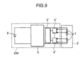
- As shown in
Fig. 9 , for example, there has been proposed a light emitting diode drive device having the following structure. That is, adrive circuit section 3 receives electric power from apower supply 8, converts the electric power into a predetermined direct-current voltage, and applies the direct-current voltage to alight source 2. Thelight source 2 includes a plurality oflight emitting diodes 1, and a plurality of voltage detection circuit sections 4' each detect a voltage across the relevantlight emitting diode 1. An abnormality detection circuit section 5' detects an abnormality of eachlight emitting diode 1, based on the voltage detected by the voltage detection circuit section 4'. Moreover, there has also been proposed a light emitting diode drive device having the following structure. That is, a plurality of light emitting diodes are divided into several sets, and an abnormality detection circuit section detects a voltage across each set. - The light emitting diode drive device including the abnormality detection circuit section described above can widely detect electrical abnormalities such as a short circuit and a break of the light emitting diode. However, the light emitting diode drive device needs to detect the voltage at each of the plurality of light emitting diodes. Consequently, the light emitting diode drive device requires the voltage detection circuit sections 4' which are equal in number to the plurality of light emitting diodes. This structure complicates a circuit configuration.
- Patent Document 1: Japanese Unexamined Patent Publication No.
Hei 9-288456 - Patent Document 2: Japanese Unexamined Patent Publication No.
2006-210835 - The present invention has been devised in view of the circumstances described above, and one object thereof is to provide a light emitting diode drive device for applying a direct-current voltage to a light source including a plurality of light emitting diodes connected in series to allow the light source to light up. This light emitting diode drive device can determine whether or not the light emitting diode, which lights up, is short-circuited with a simple circuit configuration as compared with a conventional light emitting diode drive device having circuitry for detecting voltages at a plurality of light emitting diodes. Moreover, this light emitting diode drive device can be manufactured with smaller manufacturing steps at lower manufacturing cost as compared with a conventional light emitting diode drive device including a plurality of voltage detection circuit sections. Another object of the present invention is to provide an illumination device, an in-vehicle cabin illumination device and a vehicle illumination device each employing the light emitting diode drive device.
- Objects, features and advantages of the present invention will become more apparent from the following detailed description and the attached drawings.
-
-
Fig. 1 shows a schematic circuit configuration of a light emitting diode drive device according to a first embodiment of the present invention. -
Fig. 2 shows a circuit configuration of the light emitting diode drive device according to the first embodiment of the present invention. -
Fig. 3 shows a circuit configuration of the light emitting diode drive device according to the first embodiment of the present invention. -
Fig. 4 shows a graph of a correlation between a detected voltage and a time in the light emitting diode drive device according to the first embodiment of the present invention. -
Fig. 5 shows a schematic circuit configuration of a power supply in the first embodiment of the present invention. -
Fig. 6 shows a circuit configuration of a light emitting diode drive device according to a second embodiment of the present invention. -
Fig. 7 shows a circuit configuration of a light emitting diode drive device according to a third embodiment of the present invention. -
Fig. 8 shows a block diagram of a malfunction determination circuit section in the light emitting diode drive device according to the third embodiment of the present invention. -
Fig. 9 shows a schematic circuit configuration of a conventional light emitting diode drive device. - The following embodiments will exemplify a light emitting diode drive device for use in a headlight of a vehicle.
- A circuit configuration and operations of a light emitting diode drive device A according to the present embodiment will be described with reference to
Figs. 1 through 6 . - First, the basic circuit configuration of the light emitting diode drive device A according to the present embodiment is described with reference to
Fig. 1 . - The light emitting diode drive device A according to the present embodiment includes a
drive circuit section 3 that converts electric power supplied from apower supply 8 into a direct-current voltage and outputs the direct-current voltage, a voltagedetection circuit section 4 that detects a voltage across alight source 2 including a plurality oflight emitting diodes 1 connected in series, a malfunctiondetermination circuit section 5 that determines whether or not thelight emitting diode 1, which lights up, is short-circuited, based on the voltage detected by the voltagedetection circuit section 4, adisplay section 6 that displays the result of determination by the malfunctiondetermination circuit section 5, and a currentdetection circuit section 7 that detects an electric current to be fed to thelight source 2. - In the present embodiment, the
power supply 8 for supplying electric power to the light emitting diode drive device A is a battery that outputs a direct-current voltage. Thepower supply 8 has an output terminal connected with an input side of thedrive circuit section 3. Thedrive circuit section 3 boosts the direct-current voltage output from thepower supply 8, and outputs the boosted direct-current voltage through an output side thereof. Thelight source 2 is connected to the output side of thedrive circuit section 3 and receives the boosted direct-current voltage, so that the plurality oflight emitting diodes 1, which form thelight source 2, each emit light. The voltagedetection circuit section 4 includesvoltage detection resistors light source 2. Thevoltage detection resistors light source 2 and output the divided voltage. This divided voltage is proportional to the voltage across thelight source 2, and therefore allows detection of the voltage across thelight source 2. The currentdetection circuit section 7 includes acurrent detection resistor 7a. Thecurrent detection resistor 7a outputs a voltage drop at thecurrent detection resistor 7a in a form of signal voltage. This signal voltage is proportional to an electric current flowing through thelight source 2, and therefore allows detection of the electric current flowing through thelight source 2. The malfunctiondetermination circuit section 5 determines whether or not thelight emitting diode 1, which lights up, is short-circuited, based on the detected divided voltage. Thedisplay section 6 displays the fact that thelight emitting diode 1 is short-circuited or is not short-circuited, which is determined by the malfunctiondetermination circuit section 5. - Next, a configuration and operations of the
drive circuit section 3 are described with reference toFig. 2. Fig. 2 shows a simplified portion regarding PWM control. - In the present embodiment, the
drive circuit section 3 is abooster converter 3a which is a step-up type switching power supply circuit. Thebooster converter 3a serving as thedrive circuit section 3 boosts a direct-current voltage from thepower supply 8 to output a required voltage, and then supplies the voltage to thelight source 2. - The
booster converter 3a includes aninductor 9 having a first end connected to a high-voltage side of thepower supply 8, abackflow prevention diode 10 having an anode connected to a second end of theinductor 9, acapacitor 11 connected between a cathode side of thediode 10 and a low-voltage side of thepower supply 8, and aswitch element 12 connected between the anode side of thediode 10 and the low-voltage side of thepower supply 8. Examples of theswitch element 12 may include a power MOSFET (Metal Oxide Semiconductor Field Effect Transistor) and the like. - The
capacitor 11 is electrically charged when theswitch element 12 is turned off while theinductor 9 receives electric current when theswitch element 12 is turned on. Herein, the electric current flowing through theinductor 9 increases because of self induction as a time elapses. When theswitch element 12 is turned off again, no electric current flows through theinductor 9 and a magnetic flux formed by the electric current in theinductor 9 decreases, so that there occurs a change in magnetic flux. Accordingly, an inverted electromotive force is generated in a direction that the change in magnetic force is prevented, that is, a direction that an electric current is continuously fed to theinductor 9. The voltage across the capacitor 11 (the output voltage) is generated in such a manner that a voltage based on the inverted electromotive force generated in theinductor 9 is superimposed on a voltage based on the electrical charge in thecapacitor 11 in the state in which theswitch element 12 is turned off. As a result, the resultant voltage is equal to or more than the voltage at thepower supply 8. By use of this voltage, theswitch element 12 is turned on and off periodically to boost the voltage. - The magnitude of the inverted electromotive force generated at the
inductor 9 depends on the magnitude of the formed magnetic flux, and therefore the inverted electromotive force becomes large as the electric current flowing through theinductor 9 is large. Moreover, since the electric current increases as a time elapses, the magnitude of the output direct-current voltage becomes high as the ON period of theswitch element 12 is long. A change in ratio between the ON period and the OFF period of theswitch element 12 in one cycle allows a change in magnitude of the direct-current voltage to be output from thebooster converter 3a. - Typically, control for changing a ratio between an ON period and an OFF period of a switch element in one cycle is referred to as duty control. Moreover, a method for controlling an output from a converter or the like in accordance with the duty control is referred to as PWM (Pulse Width Modulation) control.
- In the present embodiment, the output from the
booster converter 3a is controlled using this PWM control, so that the electric power to be supplied to thelight source 2 is set suitable for light emission from thelight source 2 and is kept at a certain level. When the electric power to be supplied to thelight source 2 is kept at a certain level, the intensity of light emitted from thelight emitting diode 1 becomes stable. Thus, it is possible to determine whether thelight emitting diode 1, which lights up, is short-circuited, with stable accuracy. -
Fig. 3 shows details of the PWM control which is shown inFig. 2 in a simplified manner. The PWM control is described with reference toFig. 3 . - In order to perform the PWM control, the
booster converter 3a includes a PWMcontrol circuit section 13 and adriver circuit section 18. The PWMcontrol circuit section 13 includes a powersupply circuit section 14, a reference valuegeneration circuit section 16 and a PWM control signalgeneration circuit section 17. - The power
supply circuit section 14 receives the electric power from thepower supply 8 to generate an operating power supply voltage for the PWMcontrol circuit section 13, and drives the PWMcontrol circuit section 13. Anamplification circuit section 15 includes a dividedvoltage amplifier 15a and asignal voltage amplifier 15b. Theamplification circuit section 15 amplifies a divided voltage to output an amplified divided voltage, and also amplifies a signal voltage to output an amplified signal voltage. The amplified divided voltage is input to the reference valuegeneration circuit section 16 through the PWM control signalgeneration circuit section 17. The reference valuegeneration circuit section 16 divides a target electric power value set therein by the amplified divided voltage to set a target electric current to be fed to thelight source 2, and generates a reference voltage corresponding to the set target electric current. The PWM control signalgeneration circuit section 17 compares the amplified signal voltage with a reference voltage, and generates a PWM control signal corresponding to the difference between the amplified signal voltage and the reference voltage. Adriver circuit section 18 receives the PWM control signal to output a drive signal for controlling the ON/OFF state of theswitch element 12 of thebooster converter 3a. Thebooster converter 3a is subjected to the PWM control, based on this drive signal, and the output therefrom is kept at a certain level. - Next, operations of the malfunction
determination circuit section 5 for determining the short circuit of thelight emitting diode 1 are described with reference toFig. 2 andFig. 4 . - The malfunction
determination circuit section 5 includes afirst holding section 19 that holds a divided voltage of the voltage across the light source 2 (herein, the divided voltage is detected by the voltage detection circuit section 4) every predetermined sampling time T, asecond holding section 20 that holds the divided voltage held by thefirst holding section 19 before thefirst holding section 19 holds a new divided voltage (i.e., a divided voltage acquired at a preceding sampling timing), a time settingcircuit section 21 that sets the sampling time T, adifferential circuit section 22 that outputs a differential value between the voltage held by thefirst holding section 19 and the voltage held by thesecond holding section 20, a threshold valuesetting circuit section 23 that sets a threshold value for determining whether or not the output from thedifferential circuit section 22 is adequate to a short circuit of thelight emitting diode 1, and acomparison circuit section 24 that compares the output from thedifferential circuit section 22 with the threshold value to determine whether or not thelight emitting diode 1 is short-circuited. - In
Fig. 4 , a lateral axis indicates a time, in which "t1", "t2", ... and "t6" each represent a timing that thefirst holding section 19 holds a divided voltage detected by the voltagedetection circuit section 4. On the other hand, a vertical axis indicates a voltage, in which "ΔV" represents a value of drop of the voltage across thelight source 2 in a case where onelight emitting diode 1 is short-circuited. - The case where the detected divided voltage is held at the timing t3 and the timing t4 is described. The divided voltage detected by the voltage
detection circuit section 4 is held by thefirst holding section 19 at the timing t3. After a lapse of the sampling time T set by the time settingcircuit section 21, in other words, at the timing t4, the divided voltage, which is detected at the timing t3 and is held by thefirst holding section 19, is transferred to thesecond holding section 20 and is held by thesecond holding section 20. Thereafter, the divided voltage, which is detected at the timing t4, is held by thefirst holding section 19. Herein, thedifferential circuit section 22 outputs a differential value between the divided voltage held by thefirst holding section 19 and the divided voltage held by thesecond holding section 20. Thecomparison circuit section 24 compares the threshold value with the output from thedifferential circuit section 22, and when the output from thedifferential circuit section 22 is equal to or more than the threshold value, determines that thelight emitting diode 1 is short-circuited. - When the
light emitting diode 1, which lights up, is short-circuited, the voltage across thelight source 2 is changed by an amount corresponding to a forward voltage at the short-circuitedlight emitting diode 1. Therefore, the threshold value is set with the forward voltage at onelight emitting diode 1 used as a reference. However, the change of the voltage across thelight source 2 because of the short circuit of thelight emitting diode 1 depends on variations in characteristics of thelight emitting diodes 1 in the process of manufacture, variations in voltage output from thepower supply 8, and a secular change of thelight emitting diode 1 caused by an ambient temperature and a light emitting operation. Accordingly, these factors occasionally lower accuracy of determining whether thelight emitting diode 1, which lights up, is short-circuited. In order to prevent this disadvantage, the threshold value can be changed by the threshold valuesetting circuit section 23. For example, the threshold valuesetting circuit section 23 can change the threshold value, based on an external input signal. Alternatively, the light emitting diode drive device A may be provided with a knob for changing the settings, and this knob may be operated for changing the threshold value. - Moreover, the length of the sampling time T also exerts an adverse influence on the accuracy of determination about the short circuit, and therefore can be changed by the time setting
circuit section 21. As in the case of the threshold value, for example, the time settingcircuit section 21 can change the sampling time T, based on an external input signal. Alternatively, the light emitting diode drive device A may be provided with a knob for changing the settings, and this knob may be turned for changing the sampling time T. - Next, operations of the malfunction
determination circuit section 5 after determining that thelight emitting diode 1 is short-circuited or is not short-circuited will be described. - The result of determination by the malfunction
determination circuit section 5, that is, the fact that thelight emitting diode 1 is short-circuited or is not short-circuited is stored in a memory circuit section 40 (seeFig. 1 ) which is a nonvolatile memory circuit, for example. Thedisplay section 6 receives the result from thememory circuit section 40, and displays the fact that thelight emitting diode 1 is short-circuited or is not short-circuited. Thedisplay section 6 is provided on a panel display section in an operating seat. Thus, a user can readily check the fact that thelight emitting diode 1 is short-circuited or is not short-circuited, and when thelight emitting diode 1 is short-circuited, thedisplay section 6 prompts the user to repair the short-circuitedlight emitting diode 1. - In accordance with the fact that the
light emitting diode 1 is short-circuited or is not short-circuited, which is stored in thememory circuit section 40, the electric power to be supplied to thelight source 2 is restricted upon emission of light again. More specifically, in order to drive the light emitting diode drive device A, the PWM control signalgeneration circuit section 17 determines whether or not thememory circuit section 40 stores therein the fact that thelight emitting diode 1 is short-circuited. When thememory circuit section 40 stores therein the fact that thelight emitting diode 1 is short-circuited, the PWM control signalgeneration circuit section 17 turns theswitch element 12 off, for example. Thus, since no voltage is boosted by thedrive circuit section 3, no electric power is supplied to thelight source 2. This configuration makes it possible to prevent continuous use of thelight source 2 with a reduced quantity of light. - The output voltage from the
power supply 8 is set at a voltage having a value obtained by multiplying a numeric value which is smaller by one than the number oflight emitting diodes 1 in thelight source 2 by a value of a forward ON voltage at thelight emitting diode 1, that is, a voltage which is lower than a threshold voltage required for allowing thelight source 2 to light up in a state in which one of thelight emitting diodes 1 is short-circuited. - In the present embodiment, the
power supply 8 is a battery for outputting a direct-current voltage; however, the present invention is not limited thereto. Alternatively, thepower supply 8 may include an alternating-current power supply 8a. With this configuration, the PWM control signalgeneration circuit section 17 turns theswitch element 12 off to lower the voltage to be applied to thelight source 2 to a level below the threshold voltage, so that thelight source 2 is turned out. - As shown in
Fig. 5 , thepower supply 8 including the alternating-current power supply 8a also includes a rectifyingdiode 33 that rectifies an alternating current, and a smoothingcapacitor 34 that smoothes the electric current rectified by the rectifyingdiode 33. Herein, two ends of the smoothingcapacitor 34 serve as output terminals of thepower supply 8. - As shown in
Fig. 6 , a light emitting diode drive device A according to the present embodiment is different from the light emitting diode drive device A according to the first embodiment in a point that aflyback converter 3b including aflyback transformer 28 is provided in place of thedrive circuit section 3. In the present embodiment, the remaining configuration is similar to that described in the first embodiment. In the present embodiment, constituent members identical with those in the first embodiment are denoted with the identical reference signs, and therefore the description thereof will not be given. - A configuration and operations of the
flyback converter 3b are described herein below with reference toFig. 6 . - The
flyback converter 3b includes aflyback transformer 28 that includes a power supply-side wire 26 wound around a core (not shown) with a first end thereof connected to a high pressure side of apower supply 8 which is a direct-current power supply and a output-side wire 27 coupled magnetically to the power supply-side wire 26 and wound around a core (not shown) in a direction opposite to that of the power supply-side wire 26, aflyback switch element 29 connected to a second end of the power supply-side wire 26 and a low pressure side of thepower supply 8, a backflow preventingflyback diode 30 having an anode connected to a first end of the output-side wire 27, and aflyback capacitor 31 connected to a cathode of theflyback diode 30 and a second end of the output-side wire 27. Herein, two ends of theflyback capacitor 31 serve as output terminals of theflyback converter 3b. Examples of theflyback switch element 29 may include a power MOSFET and the like. - During a period of time that the
flyback switch element 29 is turned on, an electric current flows through the power supply-side wire 26. The electric current flowing through the power supply-side wire 26 increases because of self induction as a time elapses. Herein, an electromotive force is generated at the output-side wire 27 because of mutual induction, but is directed inversely since the output-side wire 27 is wound inversely with respect to the power supply-side wire 26. Accordingly, theflyback diode 30 prevents the electric current from flowing through the output-side wire 27. Next, theflyback switch element 29 is turned off. When theflyback switch element 29 is turned off, a magnetic flux formed on the power supply-side wire 26 decreases. Herein, the electromotive force is generated because of the mutual induction at the output-side wire 27. This electromotive force serves as an output from theflyback converter 3b. In other words, when theflyback switch element 29 is turned on, a magnetic force is accumulated in the power supply-side wire 26. On the other hand, when theflyback switch element 29 is turned off, the magnetic force is released from the output-side wire 27. Thus, a voltage is generated at the output-side wire 27. - As described above, the electric current flowing through the power supply-
side wire 26 increases as the time elapses. For this reason, the magnetic force to be accumulated in the power supply-side wire 26 becomes strong as the ON period of theflyback switch element 29 is long, so that the output voltage becomes high. As in the case of thebooster converter 3a, it is possible to control an output from theflyback converter 3b in such a manner that theflyback converter 3b is subjected to PWM control by control of a duty ratio. - In the present embodiment, the output voltage of the
flyback converter 3b is controlled by a PWM control circuit section which is similar to that described in the first embodiment, so that electric power to be supplied to alight source 2 is set at a predetermined level and is kept constantly. - Moreover, the voltage generated by the magnetic force released from the output-
side wire 27 depends on a ratio regarding inductance between the power supply-side wire 26 and the output-side wire 27 and a duty ratio between an ON state and an OFF state of theflyback switch element 29. Therefore, the change in inductance ratio and duty ratio allows theflyback converter 3b to boost and lower a voltage. Accordingly, it is possible to realize adrive circuit section 3 irrespective of a direct-current voltage to be output from the direct-current power supply 8a. - As shown in
Fig. 7 andFig. 8 , a light emitting diode drive device according to the present embodiment is different from the light emitting diode drive device according to the first embodiment in points that amicrocomputer 25 includes a PWMcontrol circuit section 13, a malfunctiondetermination circuit section 5 and amemory circuit section 40 and thememory circuit section 40 is a flash memory. In the present embodiment, the remaining configuration is similar to that described in the first or second embodiment. In the present embodiment, constituent members identical with those in the first or second embodiment are denoted with the identical reference signs, and therefore the description thereof will not be given. - The
microcomputer 25 includes anoutput interface 36. A PWM control signal is generated by a PWM control signalgeneration circuit section 17 of the PWMcontrol circuit section 13, and is output to adriver control section 18 via theoutput interface 36. - The PWM
control circuit section 13 configured with themicrocomputer 25 can set the generation of the PWM control signal more finely, and can finely adjust electric power to be supplied to alight source 2 such that the electric power becomes stable at a certain level. Simultaneously, the malfunctiondetermination circuit section 5 configured with themicrocomputer 25 can be obtained at low cost. As described above, it is desirable that themicrocomputer 25 includes at least the PWMcontrol circuit section 13 and the malfunctiondetermination circuit section 5. - Further, it is more desirable that the
microcomputer 25 also includes thememory circuit section 40 because a circuit configuration can be simplified. In particular, thememory circuit section 40, which is in a form of flash memory, can hold data with ease even in a case where no electric power is supplied thereto from a powersupply circuit section 14. Further, thememory circuit section 40, which is in the form of flash memory, allows rewrite of the data stored therein. - The light emitting diode drive device A according to each embodiment is accommodated together with the
light source 2 in an apparatus main body (not shown) which is configured appropriately, so that an illumination device can be realized. - Alternatively, the light emitting diode drive device A according to each embodiment is accommodated together with the
light source 2 in an in-vehicle light body (not shown). As a result, the light emitting diode drive device A may be used as an in-vehicle cabin illumination device to be installed in an interior of a vehicle, or may be used as a vehicle illumination device (e.g., a headlight, an auxiliary lamp, a daytime running lamp) to be attached to a vehicle body. - As described above, according to one aspect of the present invention, there is provided a light emitting diode drive device including a drive circuit section that applies a direct-current voltage to a light source including a plurality of light emitting diodes connected in series to allow the light source to light up, a voltage detection circuit section that detects a voltage across the light source, and a malfunction determination circuit section that determines that the light emitting diode is short-circuited when the voltage detection circuit section detects a voltage drop and a potential between the voltage before being dropped and the voltage after being dropped is equal to or more than a predetermined threshold value.
- With this configuration, the light emitting diode drive device determines whether or not the light emitting diode, which lights up, is short-circuited, based on the change in voltage across the light source. Therefore, the light emitting diode drive device is simpler in circuit configuration than a conventional light emitting diode drive device that detects voltages at a plurality of light emitting diodes. Accordingly, it is possible to provide a light emitting diode drive device which is manufactured with smaller manufacturing steps at lower manufacturing cost as compared with a conventional light emitting diode drive device for detecting voltages at a plurality of light emitting diodes.
- In the configuration described above, the light emitting diode drive device further includes a display section that displays the fact that the light emitting diode is short-circuited or is not short-circuited, which is determined by the malfunction determination circuit section.
- With this configuration, a user of the light emitting diode drive device can view the fact that the light emitting diode is short-circuited or is not short-circuited, through the display section. For this reason, the light emitting diode drive device can prompt the user to repair the light emitting diode. This configuration improves the convenience for the user.
- In the configuration described above, the light emitting diode drive device further includes a memory circuit section that stores therein the fact that the light emitting diode is short-circuited or is not short-circuited, which is determined by the malfunction determination circuit section.
- With this configuration, the memory circuit section stores therein the fact that the light emitting diode is short-circuited or is not short-circuited. Therefore, in a case where the light emitting diode drive device, which is halted, is used again, the user can check the fact that the light emitting diode is short-circuited or is not short-circuited, which is stored in the memory circuit section, before a direct-current voltage is applied to the light source. Accordingly, in the case where the light emitting diode drive device, which is halted, is used again, the user can check whether or not the light source is in a usable state. The light emitting diode drive device can select an operation in accordance with the state of the light source.
- In the configuration described above, the drive circuit section checks data stored in the memory circuit section prior to the application of the direct-current voltage to the light source, and when the memory circuit section stores therein the result of determination that the light emitting diode is short-circuited, lowers the voltage to be applied to the light source to a level below a threshold voltage required for light emission from the light source.
- With this configuration, in the case where the light emitting diode drive device, which is halted, is used again, if the memory circuit section stores therein the result of determination that the light emitting diode is short-circuited, the voltage to be applied to the light source is lowered to a level below the threshold voltage for light emission from the light source. Therefore, it is possible to prevent continuous use of the light source in a state in which a quantity of light is reduced.
- In the configuration described above, the malfunction determination circuit section includes a first holding section that holds a voltage detected by the voltage detection circuit section every predetermined sampling time, a second holding section that holds the voltage held by the first holding section before the first holding section holds a new voltage, a differential circuit section that outputs a potential difference between the voltage held by the first holding section and the voltage held by the second holding section, and a comparison circuit section that determines that the light emitting diode is short-circuited, when the output from the differential circuit section is equal to or more than the threshold value.
- With this configuration, it is determined whether or not the light emitting diode, which lights up, is short-circuited, based on whether or not the change of the voltage across the light source at the predetermined sampling time is equal to or more than the threshold value. Therefore, it is possible to distinguish a voltage variation within a normal range from a voltage drop due to a short circuit of a light emitting diode. Accordingly, it is possible to determine whether or not the light emitting diode, which lights up, is short-circuited with improved accuracy.
- In the configuration described above, at least one of the sampling time and the threshold value is changeable.
- With this configuration, at least one of the sampling time and the threshold value is changeable. Therefore, it is possible to set a sampling time and a threshold value each capable of distinguishing a voltage variation within a normal range from a malfunction such as a short circuit of a light emitting diode. Herein, the voltage variation occurs in accordance with characteristics of the light emitting diodes, characteristics of the power supply for supplying electric power to the drive circuit section, a secular change of the light emitting diode because of an ambient temperature and a light emitting operation, and the like. Accordingly, it is possible to determine whether the light emitting diode, which lights up, is short-circuited with stable accuracy.
- In the configuration described above, at least one of the sampling time and the threshold value can be changed based on an external input signal.
- With this configuration, at least one of the sampling time and the threshold value can be changed using an external input signal. Therefore, it is possible to externally set a sampling time and a threshold value each capable of distinguishing a voltage variation within a normal range from a malfunction such as a short circuit of a light emitting diode. Herein, the voltage variation occurs in accordance with characteristics of the light emitting diodes, characteristics of the power supply for supplying electric power to the drive circuit section, a secular change of the light emitting diode because of an ambient temperature and a light emitting operation, and the like. Accordingly, it is possible to determine whether the light emitting diode, which lights up, is short-circuited with stable accuracy.
- In the configuration described above, the drive circuit section is a flyback converter that converts a direct-current voltage to be input thereto into a predetermined direct-current voltage, and outputs the direct-current voltage.
- With this configuration, the flyback converter serves as the drive circuit section. Therefore, it is possible to apply, to the light source, a direct-current voltage suitable for light emission from the light emitting diode by the drive circuit section even when a voltage at the power supply for supplying electric power to the light emitting diode drive device is different from a voltage for light emission from the light source.
- In the configuration described above, the drive circuit section is a step-up chopper type booster converter that boosts a direct-current voltage to be input thereto and outputs a predetermined direct-current voltage.
- With this configuration, the step-up chopper type booster converter for boosting a direct-current voltage to a predetermined level serves as the drive circuit section. Therefore, it is possible to boost a direct-current voltage to a level suitable for light emission from the light source by the drive circuit section and then to apply the boosted voltage to the light emitting diode even when a voltage at the power supply for supplying electric power to the light emitting diode drive device is lower than a voltage for light emission from the light source.
- In the configuration described above, the light emitting diode drive device further includes a current detection circuit section that detects an electric current to be fed to the light source, and a PWM control circuit section that has a reference value generation circuit section for setting a target electric current to be fed to the light source, based on the voltage detected by the voltage detection circuit section and a preset value of electric power. Herein, the PWM control circuit section controls the drive circuit section in a PWM manner such that the electric current detected by the current detection circuit section matches with the target electric current.
- With this configuration, it is possible to supply a desired amount of electric power to the light source and to keep the supplied electric power at a certain level. Accordingly, it is possible to keep a quantity of light from the light emitting diode at a desired level. Moreover, it is possible to determine whether or not the light emitting diode, which lights up, is short-circuited, with stable accuracy since the electric power is supplied stably.
- In the configuration described above, at least the PWM control circuit section and the malfunction determination circuit section are configured with a microcomputer.
- With this configuration, the PWM control circuit section is configured with the microcomputer. Therefore, it is possible to finely adjust a PWM control signal and to control electric power to be output from the drive circuit section, with good accuracy.
- Moreover, it is possible to reduce a parts count since both the PWM control circuit section and the malfunction determination circuit section are configured with the microcomputer.
- In the configuration described above, the microcomputer includes the memory circuit section.
- With this configuration, the memory circuit section is also configured with the microcomputer. Therefore, it is possible to simplify the circuit configuration.
- In the configuration described above, the memory circuit section is a flash memory.
- With this configuration, the flash memory serves as the memory circuit section. Therefore, it is possible to hold data even when no electric power is supplied to the light emitting diode drive device, and to readily rewrite the data.
- According to another aspect of the present invention, there is provided an illumination device including the light emitting diode drive device having any one of the configurations described above, and the light source.
- With this configuration, the illumination device employs the light emitting diode drive device described above, and therefore can be realized with a simple circuit configuration at low cost.
- According to still another aspect of the present invention, there is provided an in-vehicle cabin illumination device including the light emitting diode drive device having any one of the configurations described above, and the light source.
- With this configuration, the in-vehicle cabin illumination device employs the light emitting diode drive device described above, and therefore can be realized with a simple circuit configuration at low cost.
- According to yet another aspect of the present invention, there is provided a vehicle illumination device including the light emitting diode drive device having any one of the configurations described above, and the light source.
- With this configuration, the vehicle illumination device (e.g., a headlight, an auxiliary lamp, a daytime running lamp) employs the light emitting diode drive device described above, and therefore can be realized with a simple circuit configuration at low cost.
Claims (16)
- A light emitting diode drive device comprising:a drive circuit section that applies a direct-current voltage to a light source including a plurality of light emitting diodes connected in series to allow the light source to light up;a voltage detection circuit section that detects a voltage across the light source; anda malfunction determination circuit section that determines that the light emitting diode is short-circuited when the voltage detection circuit section detects a voltage drop and a potential between the voltage before being dropped and the voltage after being dropped is equal to or more than a predetermined threshold value.
- The light emitting diode drive device according to claim 1, further comprising
a display section that displays the fact that the light emitting diode is short-circuited or is not short-circuited, which is determined by the malfunction determination circuit section. - The light emitting diode drive device according to claim 1 or 2, further comprising
a memory circuit section that stores therein the fact that the light emitting diode is short-circuited or is not short-circuited, which is determined by the malfunction determination circuit section. - The light emitting diode drive device according to claim 3, wherein:the drive circuit section checks data stored in the memory circuit section prior to the application of the direct-current voltage to the light source, and when the memory circuit section stores therein the result of determination that the light emitting diode is short-circuited, lowers the voltage to be applied to the light source to a level below a threshold voltage required for light emission from the light source.
- The light emitting diode drive device according to any one of claims 1 through 4, wherein:the malfunction determination circuit section includes:a first holding section that holds a voltage detected by the voltage detection circuit section every predetermined sampling time;a second holding section that holds the voltage held by the first holding section before the first holding section holds a new voltage;a differential circuit section that outputs a potential difference between the voltage held by the first holding section and the voltage held by the second holding section; anda comparison circuit section that determines that the light emitting diode is short-circuited, when the output from the differential circuit section is equal to or more than the threshold value.
- The light emitting diode drive device according to claim 5, wherein:at least one of the sampling time and the threshold value is changeable.
- The light emitting diode drive device according to claim 5, wherein:at least one of the sampling time and the threshold value can be changed based on an external input signal.
- The light emitting diode drive device according to any one of claims 1 through 7, wherein:the drive circuit section is a flyback converter that converts a direct-current voltage to be input thereto into a predetermined direct-current voltage, and outputs the direct-current voltage.
- The light emitting diode drive device according to any one of claims 1 through 7, wherein:the drive circuit section is a step-up chopper type booster converter that boosts a direct-current voltage to be input thereto and outputs a predetermined direct-current voltage.
- The light emitting diode drive device according to claim 8 or 9, further comprising:a current detection circuit section that detects an electric current to be fed to the light source; anda PWM control circuit section that has a reference value generation circuit section for setting a target electric current to be fed to the light source, based on the voltage detected by the voltage detection circuit section and a preset value of electric power, wherein:the PWM control circuit section controls the drive circuit section in a PWM manner such that the electric current detected by the current detection circuit section matches with the target electric current.
- The light emitting diode drive device according to claim 10, wherein:at least the PWM control circuit section and the malfunction determination circuit section are configured with a microcomputer.
- The light emitting diode drive device according to claim 11, further comprising
a memory circuit section that stores therein the fact that the light emitting diode is short-circuited or is not short-circuited, which is determined by the malfunction determination circuit section, wherein:the microcomputer includes the memory circuit section. - The light emitting diode drive device according to claim 12, wherein:the memory circuit section is a flash memory.
- An illumination device comprising the light emitting diode drive device according to any one of claims 1 through 13, and the light source.
- An in-vehicle cabin illumination device comprising the light emitting diode drive device according to any one of claims 1 through 13, and the light source.
- A vehicle illumination device comprising the light emitting diode drive device according to any one of claims 1 through 13, and the light source.
Applications Claiming Priority (2)
| Application Number | Priority Date | Filing Date | Title |
|---|---|---|---|
| JP2007279684A JP2009111035A (en) | 2007-10-26 | 2007-10-26 | Light emitting diode drive device, illumination device using light emitting diode drive device, in-vehicle cabin illumination device, and vehicle illumination device |
| PCT/JP2008/067394 WO2009054224A1 (en) | 2007-10-26 | 2008-09-26 | Light emitting diode drive device, illumination device, in-vehicle cabin illumination device, and vehicle illumination device |
Publications (3)
| Publication Number | Publication Date |
|---|---|
| EP2204856A1 true EP2204856A1 (en) | 2010-07-07 |
| EP2204856A4 EP2204856A4 (en) | 2014-03-19 |
| EP2204856B1 EP2204856B1 (en) | 2017-11-08 |
Family
ID=40579331
Family Applications (1)
| Application Number | Title | Priority Date | Filing Date |
|---|---|---|---|
| EP08841637.5A Not-in-force EP2204856B1 (en) | 2007-10-26 | 2008-09-26 | Light emitting diode drive device, illumination device, in-vehicle cabin illumination device, and vehicle illumination device |
Country Status (5)
| Country | Link |
|---|---|
| US (1) | US8362639B2 (en) |
| EP (1) | EP2204856B1 (en) |
| JP (1) | JP2009111035A (en) |
| CN (1) | CN101842914B (en) |
| WO (1) | WO2009054224A1 (en) |
Cited By (8)
| Publication number | Priority date | Publication date | Assignee | Title |
|---|---|---|---|---|
| EP2605620A1 (en) * | 2011-12-16 | 2013-06-19 | Samsung Electro-Mechanics Co., Ltd. | LED driving apparatus and method of driving LED |
| US20130176031A1 (en) * | 2012-01-10 | 2013-07-11 | Sirius Light Technology Co., Ltd. | Apparatus for detecting abnormality in an led vehicle lamp |
| WO2014204971A2 (en) | 2013-06-18 | 2014-12-24 | Dialight Corporation | Long life, fail safe traffic light |
| EP2244531A3 (en) * | 2008-11-25 | 2015-06-10 | Panasonic Intellectual Property Management Co., Ltd. | Lighting device |
| EP2998789A1 (en) * | 2014-09-04 | 2016-03-23 | Koito Manufacturing Co., Ltd. | Vehicle lamp device and abnormality detector of light source thereof |
| US9658274B2 (en) | 2011-07-05 | 2017-05-23 | Nec Lighting Ltd. | Light-emitting element failure detector and method for detecting light-emitting element failure |
| US9709637B2 (en) | 2011-07-04 | 2017-07-18 | Nec Lighting, Ltd. | Light-emitting element failure detector and method for detecting light-emitting element failure |
| WO2020173712A1 (en) * | 2019-02-27 | 2020-09-03 | Osram Opto Semiconductors Gmbh | Device and method for replacing at least one chip |
Families Citing this family (37)
| Publication number | Priority date | Publication date | Assignee | Title |
|---|---|---|---|---|
| WO2011030381A1 (en) * | 2009-09-10 | 2011-03-17 | 三菱電機株式会社 | Led lighting apparatus for head lamp, and head lamp lighting system for vehicle |
| JP5576638B2 (en) * | 2009-11-06 | 2014-08-20 | パナソニック株式会社 | Lighting device and headlight lighting device, headlight, vehicle using the same |
| JP2011203593A (en) * | 2010-03-26 | 2011-10-13 | Panasonic Corp | Electronic flash apparatus |
| CN102725685A (en) * | 2010-02-01 | 2012-10-10 | 松下电器产业株式会社 | Light emitting element drive device and mobile apparatus |
| JP2011162008A (en) * | 2010-02-08 | 2011-08-25 | Mitsubishi Electric Corp | Led lighting device for head lamp |
| JP2011198913A (en) * | 2010-03-18 | 2011-10-06 | Nec Access Technica Ltd | Light-emitting device driving device and method |
| JP5537286B2 (en) * | 2010-06-28 | 2014-07-02 | パナソニック株式会社 | LED lighting device |
| JP5622460B2 (en) * | 2010-07-05 | 2014-11-12 | オリンパス株式会社 | Endoscope device |
| JP5056921B2 (en) * | 2010-08-24 | 2012-10-24 | カシオ計算機株式会社 | Semiconductor light source device, semiconductor light source control method, and projection device |
| US8400076B2 (en) * | 2010-10-07 | 2013-03-19 | Century Concept Ltd. | Current leakage protection device for LED applications |
| JP5760171B2 (en) | 2010-12-28 | 2015-08-05 | パナソニックIpマネジメント株式会社 | LED lighting device and lighting apparatus using the same |
| EP2487999A1 (en) * | 2011-02-09 | 2012-08-15 | National Semiconductor Corporation | Technique for identifying at least one faulty light emitting diode in multiple strings of light emitting diodes |
| EP2487998A1 (en) * | 2011-02-09 | 2012-08-15 | National Semiconductor Corporation | Technique for identifying at least one faulty light emitting diode in a string of light emitting diodes |
| TWI425661B (en) * | 2011-05-13 | 2014-02-01 | Ruei Jen Chen | Light emitting diode device |
| KR101875220B1 (en) * | 2011-06-08 | 2018-07-06 | 매그나칩 반도체 유한회사 | Led driver circuit |
| US9192014B2 (en) * | 2011-07-19 | 2015-11-17 | Nxp B.V. | LED short circuit protection |
| JP5214003B2 (en) * | 2011-08-12 | 2013-06-19 | シャープ株式会社 | Power supply device and lighting device |
| US8796930B2 (en) * | 2011-09-07 | 2014-08-05 | JST Performance, Inc. | LED device with power removal detection and method for using the same |
| JP5962946B2 (en) * | 2011-11-21 | 2016-08-03 | パナソニックIpマネジメント株式会社 | LIGHT EMITTING ELEMENT LIGHTING DEVICE AND LIGHTING DEVICE HAVING THE CIRCUIT |
| JP5984203B2 (en) * | 2012-03-05 | 2016-09-06 | Necライティング株式会社 | Method and circuit for detecting short circuit failure in organic EL element |
| JP6054620B2 (en) | 2012-03-29 | 2016-12-27 | トランスフォーム・ジャパン株式会社 | Compound semiconductor device and manufacturing method thereof |
| JP2014002946A (en) * | 2012-06-19 | 2014-01-09 | Sanken Electric Co Ltd | Power supply for led illumination |
| DE102012013039B4 (en) * | 2012-06-29 | 2020-07-23 | Diehl Aerospace Gmbh | Lighting device and method for operating the lighting device in a dimming mode |
| CN103048605B (en) * | 2012-12-22 | 2015-10-14 | 三峡电力职业学院 | The detection screening technique that a kind of LED is aging |
| JP6160955B2 (en) * | 2013-07-10 | 2017-07-12 | パナソニックIpマネジメント株式会社 | LIGHT EMITTING DIODE DRIVING DEVICE, VEHICLE LIGHTING DEVICE HAVING THE SAME, AND VEHICLE |
| KR101489948B1 (en) * | 2014-06-23 | 2015-02-06 | 유원엘디에스(주) | Method for judging quality of LED element and LED module and Apparatus for judging quality of LED element and LED module |
| DE102015105914B3 (en) | 2015-04-17 | 2016-08-11 | Siteco Beleuchtungstechnik Gmbh | Method and device for determining a life expectancy information of an LED module |
| CN107454704B (en) * | 2016-05-31 | 2020-04-03 | 西门子瑞士有限公司 | Light alarm |
| KR101694899B1 (en) * | 2016-07-13 | 2017-01-10 | 현대아이티에스전자(주) | LED electronic display board controller for detecting error and method for detecting error thereof |
| WO2018198284A1 (en) * | 2017-04-27 | 2018-11-01 | 三菱電機株式会社 | Semiconductor light source lighting device and vehicle lamp |
| CN107300665A (en) * | 2017-06-13 | 2017-10-27 | 江苏固立得精密光电有限公司 | A kind of LED chip pressure drop method for monitoring abnormality of multiple light courcess |
| CN108322959B (en) * | 2017-11-03 | 2024-03-15 | 赛尔富电子有限公司 | Dimming system of LED lamp |
| US10945324B2 (en) | 2017-11-30 | 2021-03-09 | Osram Gmbh | External assessment device for a lighting system and method of assessing a lighting system |
| JP7193529B2 (en) * | 2018-03-28 | 2022-12-20 | 株式会社小糸製作所 | Lighting circuit and vehicle lamp |
| US11495120B2 (en) * | 2018-04-10 | 2022-11-08 | Advancetrex Sensor Technologies Corp. | Universal programmable optic/acoustic signaling device with self-diagnosis |
| CN111065187B (en) * | 2018-10-17 | 2022-04-26 | 戴洛格半导体(英国)有限公司 | Current regulator |
| DE102022115153A1 (en) | 2021-07-19 | 2023-01-19 | Varroc Lighting Systems, s.r.o | METHOD AND SYSTEM FOR DETECTING LED FAILURE IN AN AUTOMOTIVE LIGHTING SYSTEM |
Citations (5)
| Publication number | Priority date | Publication date | Assignee | Title |
|---|---|---|---|---|
| US20050179393A1 (en) * | 2004-02-16 | 2005-08-18 | Koito Manufacturing Co., Ltd. | Vehicular lamp |
| US20070085494A1 (en) * | 2005-10-19 | 2007-04-19 | Koito Manufacturing Co., Ltd. | Lighting controller for lighting device for vehicle |
| US20070108843A1 (en) * | 2005-11-17 | 2007-05-17 | Preston Nigel A | Series connected power supply for semiconductor-based vehicle lighting systems |
| US20070185677A1 (en) * | 2006-01-31 | 2007-08-09 | Fujitsu Ten Limited | Vehicle abnormality detecting device |
| US20100049454A1 (en) * | 2008-08-21 | 2010-02-25 | ASIC Advanatage Inc. | Light emitting diode fault monitoring |
Family Cites Families (20)
| Publication number | Priority date | Publication date | Assignee | Title |
|---|---|---|---|---|
| JP3423529B2 (en) | 1996-04-19 | 2003-07-07 | キヤノン株式会社 | Flat panel image forming apparatus for wall installation and system for wall installation |
| JP2003249383A (en) * | 2002-02-25 | 2003-09-05 | Patoraito:Kk | Failure diagnostic circuit for led indicator |
| JP4236894B2 (en) * | 2002-10-08 | 2009-03-11 | 株式会社小糸製作所 | Lighting circuit |
| WO2004066687A1 (en) | 2003-01-17 | 2004-08-05 | Matsushita Electric Works, Ltd. | Discharge lamp lighting device, illuminating device, projector |
| JP2004296782A (en) * | 2003-03-27 | 2004-10-21 | Kyocera Corp | Led light-emitting device |
| JP3882773B2 (en) * | 2003-04-03 | 2007-02-21 | ソニー株式会社 | Image display device, drive circuit device, and light-emitting diode defect detection method |
| JP3549160B1 (en) * | 2003-05-15 | 2004-08-04 | 株式会社テクノローグ | LED degradation inspection method and device |
| JP2005093196A (en) * | 2003-09-17 | 2005-04-07 | Moritex Corp | Lighting method, and lighting system and component for the same |
| JP4093239B2 (en) | 2005-01-31 | 2008-06-04 | 松下電工株式会社 | LIGHT EMITTING DIODE DRIVING DEVICE, LIGHTING APPARATUS USING THE SAME, LIGHTING DEVICE FOR VEHICLE, LIGHTING DEVICE FOR VEHICLE |
| JP4148224B2 (en) * | 2005-01-31 | 2008-09-10 | 松下電工株式会社 | LED driving device and lighting device using the same |
| JP4640248B2 (en) | 2005-07-25 | 2011-03-02 | 豊田合成株式会社 | Light source device |
| JP4744966B2 (en) * | 2005-07-26 | 2011-08-10 | パナソニック電工株式会社 | DC power supply device for light emitting diode and lighting apparatus using the same |
| JP2007109747A (en) | 2005-10-12 | 2007-04-26 | Stanley Electric Co Ltd | Led lighting controller |
| JP2007161012A (en) * | 2005-12-12 | 2007-06-28 | Koito Mfg Co Ltd | Vehicular light emission device |
| JP5085033B2 (en) * | 2005-12-12 | 2012-11-28 | 株式会社小糸製作所 | Light emitting device for vehicle |
| JP2007182158A (en) * | 2006-01-10 | 2007-07-19 | Koito Mfg Co Ltd | Lighting control device of lighting fixture for vehicle |
| JP2007200610A (en) * | 2006-01-24 | 2007-08-09 | Koito Mfg Co Ltd | Lighting control device of vehicular lamp |
| TWI299405B (en) | 2006-03-02 | 2008-08-01 | Macroblock Inc | Method and apparatus for silent current detection |
| US7675245B2 (en) * | 2007-01-04 | 2010-03-09 | Allegro Microsystems, Inc. | Electronic circuit for driving a diode load |
| EP2129192A4 (en) | 2007-02-19 | 2012-05-30 | Panasonic Corp | Discharge lamp operation device, illumination device, and liquid crystal display device |
-
2007
- 2007-10-26 JP JP2007279684A patent/JP2009111035A/en active Pending
-
2008
- 2008-09-26 CN CN2008801140261A patent/CN101842914B/en active Active
- 2008-09-26 EP EP08841637.5A patent/EP2204856B1/en not_active Not-in-force
- 2008-09-26 WO PCT/JP2008/067394 patent/WO2009054224A1/en active Application Filing
- 2008-09-26 US US12/738,119 patent/US8362639B2/en active Active
Patent Citations (5)
| Publication number | Priority date | Publication date | Assignee | Title |
|---|---|---|---|---|
| US20050179393A1 (en) * | 2004-02-16 | 2005-08-18 | Koito Manufacturing Co., Ltd. | Vehicular lamp |
| US20070085494A1 (en) * | 2005-10-19 | 2007-04-19 | Koito Manufacturing Co., Ltd. | Lighting controller for lighting device for vehicle |
| US20070108843A1 (en) * | 2005-11-17 | 2007-05-17 | Preston Nigel A | Series connected power supply for semiconductor-based vehicle lighting systems |
| US20070185677A1 (en) * | 2006-01-31 | 2007-08-09 | Fujitsu Ten Limited | Vehicle abnormality detecting device |
| US20100049454A1 (en) * | 2008-08-21 | 2010-02-25 | ASIC Advanatage Inc. | Light emitting diode fault monitoring |
Non-Patent Citations (1)
| Title |
|---|
| See also references of WO2009054224A1 * |
Cited By (11)
| Publication number | Priority date | Publication date | Assignee | Title |
|---|---|---|---|---|
| EP2244531A3 (en) * | 2008-11-25 | 2015-06-10 | Panasonic Intellectual Property Management Co., Ltd. | Lighting device |
| US9709637B2 (en) | 2011-07-04 | 2017-07-18 | Nec Lighting, Ltd. | Light-emitting element failure detector and method for detecting light-emitting element failure |
| US9658274B2 (en) | 2011-07-05 | 2017-05-23 | Nec Lighting Ltd. | Light-emitting element failure detector and method for detecting light-emitting element failure |
| EP2605620A1 (en) * | 2011-12-16 | 2013-06-19 | Samsung Electro-Mechanics Co., Ltd. | LED driving apparatus and method of driving LED |
| US20130176031A1 (en) * | 2012-01-10 | 2013-07-11 | Sirius Light Technology Co., Ltd. | Apparatus for detecting abnormality in an led vehicle lamp |
| EP2628641A1 (en) * | 2012-01-10 | 2013-08-21 | Sirius Light Technology Co., Ltd | Apparatus for detecting abnormality in an led vehicle lamp |
| WO2014204971A2 (en) | 2013-06-18 | 2014-12-24 | Dialight Corporation | Long life, fail safe traffic light |
| EP3011806A4 (en) * | 2013-06-18 | 2017-03-08 | Dialight Corporation | Long life, fail safe traffic light |
| EP2998789A1 (en) * | 2014-09-04 | 2016-03-23 | Koito Manufacturing Co., Ltd. | Vehicle lamp device and abnormality detector of light source thereof |
| US9880106B2 (en) | 2014-09-04 | 2018-01-30 | Koito Manaufacturing Co., Ltd. | Vehicle lamp device and abnormality detector of light source thereof |
| WO2020173712A1 (en) * | 2019-02-27 | 2020-09-03 | Osram Opto Semiconductors Gmbh | Device and method for replacing at least one chip |
Also Published As
| Publication number | Publication date |
|---|---|
| US8362639B2 (en) | 2013-01-29 |
| WO2009054224A1 (en) | 2009-04-30 |
| EP2204856A4 (en) | 2014-03-19 |
| EP2204856B1 (en) | 2017-11-08 |
| US20100225235A1 (en) | 2010-09-09 |
| JP2009111035A (en) | 2009-05-21 |
| CN101842914A (en) | 2010-09-22 |
| CN101842914B (en) | 2012-01-18 |
Similar Documents
| Publication | Publication Date | Title |
|---|---|---|
| EP2204856B1 (en) | Light emitting diode drive device, illumination device, in-vehicle cabin illumination device, and vehicle illumination device | |
| JP6160955B2 (en) | LIGHT EMITTING DIODE DRIVING DEVICE, VEHICLE LIGHTING DEVICE HAVING THE SAME, AND VEHICLE | |
| JP4148224B2 (en) | LED driving device and lighting device using the same | |
| JP4093239B2 (en) | LIGHT EMITTING DIODE DRIVING DEVICE, LIGHTING APPARATUS USING THE SAME, LIGHTING DEVICE FOR VEHICLE, LIGHTING DEVICE FOR VEHICLE | |
| US8581512B2 (en) | Light source module, lighting apparatus, and illumination device using the same | |
| RU2563042C2 (en) | Light diode circuit layout | |
| JP5237727B2 (en) | LED driving device, lighting device and lighting fixture | |
| US7034607B2 (en) | Switching constant-current power device | |
| JP4799493B2 (en) | Vehicle lighting | |
| US20070159736A1 (en) | Led-based lamp apparatus | |
| EP2369897A2 (en) | Load determination device and illumination apparatus using the same | |
| JP2006261682A (en) | Method for driving light emitting diode and circuit structure | |
| CN109936893B (en) | Vehicle headlamp illumination system and control method thereof | |
| US9167654B2 (en) | Solid light source lighting device, illumination apparatus, and illumination system | |
| CN109392220A (en) | Drive circuit, lighting apparatus and motor vehicles for light-emitting diode assembly | |
| JP4731231B2 (en) | Power supply device and vehicular lamp provided with power supply device | |
| JP2018019025A (en) | Voltage conversion circuit, LED drive circuit and control method of voltage conversion circuit | |
| US8878385B2 (en) | Apparatus for controlling power supplied to discharge lamp in response to command supplied from outside the apparatus | |
| JP4909727B2 (en) | Semiconductor device | |
| JP4506593B2 (en) | Lighting device | |
| CN112369124B (en) | Light source driving device and method thereof | |
| JP7122628B2 (en) | Illumination lighting device, lighting device, and lighting fixture | |
| CN110650563B (en) | Driver, method for controlling driver, and lighting module | |
| JP2021136705A (en) | Lighting device and luminaire | |
| JP2016081756A (en) | Discharge lamp lighting device |
Legal Events
| Date | Code | Title | Description |
|---|---|---|---|
| PUAI | Public reference made under article 153(3) epc to a published international application that has entered the european phase |
Free format text: ORIGINAL CODE: 0009012 |
|
| 17P | Request for examination filed |
Effective date: 20100422 |
|
| AK | Designated contracting states |
Kind code of ref document: A1 Designated state(s): AT BE BG CH CY CZ DE DK EE ES FI FR GB GR HR HU IE IS IT LI LT LU LV MC MT NL NO PL PT RO SE SI SK TR |
|
| AX | Request for extension of the european patent |
Extension state: AL BA MK RS |
|
| DAX | Request for extension of the european patent (deleted) | ||
| RAP1 | Party data changed (applicant data changed or rights of an application transferred) |
Owner name: PANASONIC CORPORATION |
|
| A4 | Supplementary search report drawn up and despatched |
Effective date: 20140217 |
|
| RIC1 | Information provided on ipc code assigned before grant |
Ipc: H01L 33/00 20100101AFI20140211BHEP Ipc: H05B 33/08 20060101ALI20140211BHEP |
|
| RAP1 | Party data changed (applicant data changed or rights of an application transferred) |
Owner name: PANASONIC INTELLECTUAL PROPERTY MANAGEMENT CO., LT |
|
| 17Q | First examination report despatched |
Effective date: 20160817 |
|
| GRAP | Despatch of communication of intention to grant a patent |
Free format text: ORIGINAL CODE: EPIDOSNIGR1 |
|
| INTG | Intention to grant announced |
Effective date: 20170419 |
|
| GRAS | Grant fee paid |
Free format text: ORIGINAL CODE: EPIDOSNIGR3 |
|
| GRAA | (expected) grant |
Free format text: ORIGINAL CODE: 0009210 |
|
| AK | Designated contracting states |
Kind code of ref document: B1 Designated state(s): AT BE BG CH CY CZ DE DK EE ES FI FR GB GR HR HU IE IS IT LI LT LU LV MC MT NL NO PL PT RO SE SI SK TR |
|
| REG | Reference to a national code |
Ref country code: GB Ref legal event code: FG4D |
|
| REG | Reference to a national code |
Ref country code: CH Ref legal event code: EP Ref country code: AT Ref legal event code: REF Ref document number: 944931 Country of ref document: AT Kind code of ref document: T Effective date: 20171115 |
|
| REG | Reference to a national code |
Ref country code: IE Ref legal event code: FG4D |
|
| REG | Reference to a national code |
Ref country code: DE Ref legal event code: R096 Ref document number: 602008052906 Country of ref document: DE |
|
| REG | Reference to a national code |
Ref country code: NL Ref legal event code: MP Effective date: 20171108 |
|
| REG | Reference to a national code |
Ref country code: LT Ref legal event code: MG4D |
|
| REG | Reference to a national code |
Ref country code: AT Ref legal event code: MK05 Ref document number: 944931 Country of ref document: AT Kind code of ref document: T Effective date: 20171108 |
|
| PG25 | Lapsed in a contracting state [announced via postgrant information from national office to epo] |
Ref country code: SE Free format text: LAPSE BECAUSE OF FAILURE TO SUBMIT A TRANSLATION OF THE DESCRIPTION OR TO PAY THE FEE WITHIN THE PRESCRIBED TIME-LIMIT Effective date: 20171108 Ref country code: FI Free format text: LAPSE BECAUSE OF FAILURE TO SUBMIT A TRANSLATION OF THE DESCRIPTION OR TO PAY THE FEE WITHIN THE PRESCRIBED TIME-LIMIT Effective date: 20171108 Ref country code: LT Free format text: LAPSE BECAUSE OF FAILURE TO SUBMIT A TRANSLATION OF THE DESCRIPTION OR TO PAY THE FEE WITHIN THE PRESCRIBED TIME-LIMIT Effective date: 20171108 Ref country code: NO Free format text: LAPSE BECAUSE OF FAILURE TO SUBMIT A TRANSLATION OF THE DESCRIPTION OR TO PAY THE FEE WITHIN THE PRESCRIBED TIME-LIMIT Effective date: 20180208 Ref country code: ES Free format text: LAPSE BECAUSE OF FAILURE TO SUBMIT A TRANSLATION OF THE DESCRIPTION OR TO PAY THE FEE WITHIN THE PRESCRIBED TIME-LIMIT Effective date: 20171108 Ref country code: NL Free format text: LAPSE BECAUSE OF FAILURE TO SUBMIT A TRANSLATION OF THE DESCRIPTION OR TO PAY THE FEE WITHIN THE PRESCRIBED TIME-LIMIT Effective date: 20171108 |
|
| PG25 | Lapsed in a contracting state [announced via postgrant information from national office to epo] |
Ref country code: BG Free format text: LAPSE BECAUSE OF FAILURE TO SUBMIT A TRANSLATION OF THE DESCRIPTION OR TO PAY THE FEE WITHIN THE PRESCRIBED TIME-LIMIT Effective date: 20180208 Ref country code: GR Free format text: LAPSE BECAUSE OF FAILURE TO SUBMIT A TRANSLATION OF THE DESCRIPTION OR TO PAY THE FEE WITHIN THE PRESCRIBED TIME-LIMIT Effective date: 20180209 Ref country code: HR Free format text: LAPSE BECAUSE OF FAILURE TO SUBMIT A TRANSLATION OF THE DESCRIPTION OR TO PAY THE FEE WITHIN THE PRESCRIBED TIME-LIMIT Effective date: 20171108 Ref country code: LV Free format text: LAPSE BECAUSE OF FAILURE TO SUBMIT A TRANSLATION OF THE DESCRIPTION OR TO PAY THE FEE WITHIN THE PRESCRIBED TIME-LIMIT Effective date: 20171108 Ref country code: IS Free format text: LAPSE BECAUSE OF FAILURE TO SUBMIT A TRANSLATION OF THE DESCRIPTION OR TO PAY THE FEE WITHIN THE PRESCRIBED TIME-LIMIT Effective date: 20180308 Ref country code: AT Free format text: LAPSE BECAUSE OF FAILURE TO SUBMIT A TRANSLATION OF THE DESCRIPTION OR TO PAY THE FEE WITHIN THE PRESCRIBED TIME-LIMIT Effective date: 20171108 |
|
| PG25 | Lapsed in a contracting state [announced via postgrant information from national office to epo] |
Ref country code: SK Free format text: LAPSE BECAUSE OF FAILURE TO SUBMIT A TRANSLATION OF THE DESCRIPTION OR TO PAY THE FEE WITHIN THE PRESCRIBED TIME-LIMIT Effective date: 20171108 Ref country code: CY Free format text: LAPSE BECAUSE OF FAILURE TO SUBMIT A TRANSLATION OF THE DESCRIPTION OR TO PAY THE FEE WITHIN THE PRESCRIBED TIME-LIMIT Effective date: 20171108 Ref country code: CZ Free format text: LAPSE BECAUSE OF FAILURE TO SUBMIT A TRANSLATION OF THE DESCRIPTION OR TO PAY THE FEE WITHIN THE PRESCRIBED TIME-LIMIT Effective date: 20171108 Ref country code: EE Free format text: LAPSE BECAUSE OF FAILURE TO SUBMIT A TRANSLATION OF THE DESCRIPTION OR TO PAY THE FEE WITHIN THE PRESCRIBED TIME-LIMIT Effective date: 20171108 Ref country code: DK Free format text: LAPSE BECAUSE OF FAILURE TO SUBMIT A TRANSLATION OF THE DESCRIPTION OR TO PAY THE FEE WITHIN THE PRESCRIBED TIME-LIMIT Effective date: 20171108 |
|
| REG | Reference to a national code |
Ref country code: DE Ref legal event code: R097 Ref document number: 602008052906 Country of ref document: DE |
|
| PG25 | Lapsed in a contracting state [announced via postgrant information from national office to epo] |
Ref country code: RO Free format text: LAPSE BECAUSE OF FAILURE TO SUBMIT A TRANSLATION OF THE DESCRIPTION OR TO PAY THE FEE WITHIN THE PRESCRIBED TIME-LIMIT Effective date: 20171108 Ref country code: PL Free format text: LAPSE BECAUSE OF FAILURE TO SUBMIT A TRANSLATION OF THE DESCRIPTION OR TO PAY THE FEE WITHIN THE PRESCRIBED TIME-LIMIT Effective date: 20171108 Ref country code: IT Free format text: LAPSE BECAUSE OF FAILURE TO SUBMIT A TRANSLATION OF THE DESCRIPTION OR TO PAY THE FEE WITHIN THE PRESCRIBED TIME-LIMIT Effective date: 20171108 |
|
| PLBE | No opposition filed within time limit |
Free format text: ORIGINAL CODE: 0009261 |
|
| STAA | Information on the status of an ep patent application or granted ep patent |
Free format text: STATUS: NO OPPOSITION FILED WITHIN TIME LIMIT |
|
| 26N | No opposition filed |
Effective date: 20180809 |
|
| PG25 | Lapsed in a contracting state [announced via postgrant information from national office to epo] |
Ref country code: SI Free format text: LAPSE BECAUSE OF FAILURE TO SUBMIT A TRANSLATION OF THE DESCRIPTION OR TO PAY THE FEE WITHIN THE PRESCRIBED TIME-LIMIT Effective date: 20171108 |
|
| PG25 | Lapsed in a contracting state [announced via postgrant information from national office to epo] |
Ref country code: MC Free format text: LAPSE BECAUSE OF FAILURE TO SUBMIT A TRANSLATION OF THE DESCRIPTION OR TO PAY THE FEE WITHIN THE PRESCRIBED TIME-LIMIT Effective date: 20171108 |
|
| REG | Reference to a national code |
Ref country code: CH Ref legal event code: PL |
|
| GBPC | Gb: european patent ceased through non-payment of renewal fee |
Effective date: 20180926 |
|
| REG | Reference to a national code |
Ref country code: BE Ref legal event code: MM Effective date: 20180930 |
|
| REG | Reference to a national code |
Ref country code: IE Ref legal event code: MM4A |
|
| PG25 | Lapsed in a contracting state [announced via postgrant information from national office to epo] |
Ref country code: LU Free format text: LAPSE BECAUSE OF NON-PAYMENT OF DUE FEES Effective date: 20180926 |
|
| PG25 | Lapsed in a contracting state [announced via postgrant information from national office to epo] |
Ref country code: IE Free format text: LAPSE BECAUSE OF NON-PAYMENT OF DUE FEES Effective date: 20180926 |
|
| PG25 | Lapsed in a contracting state [announced via postgrant information from national office to epo] |
Ref country code: BE Free format text: LAPSE BECAUSE OF NON-PAYMENT OF DUE FEES Effective date: 20180930 Ref country code: CH Free format text: LAPSE BECAUSE OF NON-PAYMENT OF DUE FEES Effective date: 20180930 Ref country code: LI Free format text: LAPSE BECAUSE OF NON-PAYMENT OF DUE FEES Effective date: 20180930 Ref country code: FR Free format text: LAPSE BECAUSE OF NON-PAYMENT OF DUE FEES Effective date: 20180930 |
|
| PG25 | Lapsed in a contracting state [announced via postgrant information from national office to epo] |
Ref country code: GB Free format text: LAPSE BECAUSE OF NON-PAYMENT OF DUE FEES Effective date: 20180926 |
|
| PG25 | Lapsed in a contracting state [announced via postgrant information from national office to epo] |
Ref country code: MT Free format text: LAPSE BECAUSE OF NON-PAYMENT OF DUE FEES Effective date: 20180926 |
|
| PG25 | Lapsed in a contracting state [announced via postgrant information from national office to epo] |
Ref country code: TR Free format text: LAPSE BECAUSE OF FAILURE TO SUBMIT A TRANSLATION OF THE DESCRIPTION OR TO PAY THE FEE WITHIN THE PRESCRIBED TIME-LIMIT Effective date: 20171108 |
|
| PG25 | Lapsed in a contracting state [announced via postgrant information from national office to epo] |
Ref country code: HU Free format text: LAPSE BECAUSE OF FAILURE TO SUBMIT A TRANSLATION OF THE DESCRIPTION OR TO PAY THE FEE WITHIN THE PRESCRIBED TIME-LIMIT; INVALID AB INITIO Effective date: 20080926 Ref country code: PT Free format text: LAPSE BECAUSE OF FAILURE TO SUBMIT A TRANSLATION OF THE DESCRIPTION OR TO PAY THE FEE WITHIN THE PRESCRIBED TIME-LIMIT Effective date: 20171108 |
|
| PGFP | Annual fee paid to national office [announced via postgrant information from national office to epo] |
Ref country code: DE Payment date: 20210920 Year of fee payment: 14 |
|
| REG | Reference to a national code |
Ref country code: DE Ref legal event code: R119 Ref document number: 602008052906 Country of ref document: DE |
|
| PG25 | Lapsed in a contracting state [announced via postgrant information from national office to epo] |
Ref country code: DE Free format text: LAPSE BECAUSE OF NON-PAYMENT OF DUE FEES Effective date: 20230401 |