EP2200176A1 - Adjustable integrator using a single capacitance - Google Patents
Adjustable integrator using a single capacitance Download PDFInfo
- Publication number
- EP2200176A1 EP2200176A1 EP08368021A EP08368021A EP2200176A1 EP 2200176 A1 EP2200176 A1 EP 2200176A1 EP 08368021 A EP08368021 A EP 08368021A EP 08368021 A EP08368021 A EP 08368021A EP 2200176 A1 EP2200176 A1 EP 2200176A1
- Authority
- EP
- European Patent Office
- Prior art keywords
- current
- output
- amplifier
- input
- current source
- Prior art date
- Legal status (The legal status is an assumption and is not a legal conclusion. Google has not performed a legal analysis and makes no representation as to the accuracy of the status listed.)
- Withdrawn
Links
Images


Classifications
-
- H—ELECTRICITY
- H03—ELECTRONIC CIRCUITRY
- H03F—AMPLIFIERS
- H03F1/00—Details of amplifiers with only discharge tubes, only semiconductor devices or only unspecified devices as amplifying elements
- H03F1/34—Negative-feedback-circuit arrangements with or without positive feedback
-
- G—PHYSICS
- G06—COMPUTING OR CALCULATING; COUNTING
- G06G—ANALOGUE COMPUTERS
- G06G7/00—Devices in which the computing operation is performed by varying electric or magnetic quantities
- G06G7/12—Arrangements for performing computing operations, e.g. operational amplifiers specially adapted therefor
- G06G7/18—Arrangements for performing computing operations, e.g. operational amplifiers specially adapted therefor for integration or differentiation; for forming integrals
- G06G7/184—Arrangements for performing computing operations, e.g. operational amplifiers specially adapted therefor for integration or differentiation; for forming integrals using capacitive elements
- G06G7/186—Arrangements for performing computing operations, e.g. operational amplifiers specially adapted therefor for integration or differentiation; for forming integrals using capacitive elements using an operational amplifier comprising a capacitor or a resistor in the feedback loop
Definitions
- the invention relates to a circuit and a method for an integrating amplifier which increases the input range of the charge that can be measured, and more particularly to an integrating amplifier on an IC where an internal feedback loop is added thereby eliminating the need for a another external capacitor and pad.
- an amplifier wired as an integrator could be used.
- the charge to be measured is injected into the input of the amplifier and from there is fed, via an integrating capacitance, to the output of the amplifier.
- the measurement is initiated by a current pulse on the input of the integrator.
- the integrating capacitance connected between the negative input and the output of the amplifier, collects the charge transferred by the input pulse. Because of the limited output swing of the amplifier the amount of the charge that can be measured is limited.
- the range for the charge to be measured is changed by changing the integration capacitance.
- this method requires not only an additional capacitor but an additional pad. This is a disadvantage for designs which need to be placed inside small packages and where pads are either at a premium or not at all available.
- Circuit 10 comprises an amplifier 11 a having a minus (-) and a plus (+) input, and an output OUT.
- the plus input is coupled to a reference voltage V REF , for example GROUND.
- Output OUT providing current I OUT and voltage V OUT , is coupled via pad 12b, an external integrating capacitor12a (C INT ), and pad 12c to the minus input of amplifier 11 a.
- Output OUT is also coupled via switch 14 (S1), additional pad 13b, a second external integrating capacitor 13a (C INT* ), and pad 12c to the minus input of amplifier 11a.
- charge is transferred to the capacitance to be measured by a voltage pulse causing an integration current to flow.
- the amplifier delivers this current by adjusting its output voltage.
- the integration capacitor needs to be adjusted, that is another external capacitor needs to be added .
- the disadvantage of this circuit is that it needs an additional pad and that other external capacitor, leading to a higher module cost and a bigger die area. There is presently no known way to avoid this problem.
- the below described invention is directed to a circuit arrangement which offers a novel solution.
- U.S. Patent 6,608,516 discloses a system and method for adjusting the time constant of an integrator.
- a variable time constant integrator includes an amplifier, a capacitor, and a variable gain element.
- the variable gain element may include a MDAC (Multiplying Digital to Analog Converter).
- the Patent refers to signal conditioning and uses a voltage feedback to limit the range.
- U.S. Patent Application 2007/0229161 (Killat) teaches methods and circuits for a low noise and high linear voltage-to-current converter which requires only small integration resistors.
- the circuit uses a shunt to measure the current, where a current IDC used as feedback is static and is derived from a bias voltage. Current IDC is used to set the DC operating point.
- U.S. Patent 4,059,812 (Proctor) describes a phase-locked-loop which comprises an adjustable integrator further comprising an integrating amplifier and an adjustable voltage source applied to one integrating amplifier input.
- the output of the integrating amplifier changes the set time of one or more one-shot controls feeding back to the adjustable integrator and thus to the integrating amplifier.
- an output stage comprising a current mirror
- the output of the first current source of the current mirror is coupled via the external integrating capacitor to the input of the integrating amplifier.
- the output of the second current source of the current mirror which mirrors the current of the first current source and thus the output current of the integrating amplifier, is fed back to the output of the integrating amplifier.
- the output of the first current source is also coupled to a load device, the active load, which generates the bias current for the first current source.
- the second current source replicates the output current of the first current source by a factor "m", where the factor "m” is variable and is determined by the range switching required.
- a switch is coupled between the first current source and the load device to switch off the active load for the output stage during the integration phase.
- a current mirror is used in the output stage of the amplifier which feeds back a duplicate of the output current of the amplifier to its input node. This is be done on the die (chip) without requiring an extra pad.
- the range in the present invention is not limited to the voltage output range of the amplifier.
- the present invention utilizes only one capacitor and thus requires only two pads to handle the range switching.
- the extra current I EXTRA is generated by mirroring the current I OUT in the output stage of the amplifier.
- the active load for the output stage is switched off during the integration phase.
- range switching is used to measure different charges with the same feedback capacitor (C INT ). This is achieved by a replication of the output current I OUT of the amplifier through the current mirror of the output stage which comprises a first and a second current source.
- the first current source with current I OUT is inserted between the output of the amplifier and output OUT, and the second current source with a replication factor m (relative to the first current source) and current I EXTRA is coupled between the output of the amplifier and its input node. Range switching, that is changing current I EXTRA, is accomplished by changing the replication factor m.
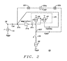
- Circuit 20 comprises an amplifier means 21 a (Amplifier) with an input 21 b and an output 21 c.
- Output 21c is coupled to output stage 25, a current mirror with current sources 26 and 27, where output 21 c is coupled to the control gates of current sources 26 and 27,.
- the output of current source 26 is output OUT providing a current I OUT .
- Output OUT is coupled via pad 22b, an external integrating capacitor means 22a (C INT ), and pad 22c to input 21 b of amplifier means 21 a.
- a switching means 24 S
- load device current source 28, the active load
- V REF reference potential
- switching means 24 is depicted as "OPEN", indicating the integration phase.
- the purpose of switching means 24 is to switch off the active load for the output stage during the integration phase to avoid a DC offset in the currents of current sources 26 and 27.
- the output of current source 27, which provides a current I EXTRA is coupled back directly to the input 21 b of amplifier means 21 a.
- the current I OUT relates to current I EXTRA as 1:m, where the selection of the replication factor "m" depends on the application.
- Amplifiers 36 and 37 represent components of current sources 26 and 27, respectively and are depicted as PMOS transistors by way of example.
- Amplifiers 36 and 37 are tied to a voltage potential +V (shown as sources of transistors ).
- the inputs of amplifiers 36 and 37 are tied together and receive their input via output 21 c (shown as gates of transistors).
- the outputs of amplifiers 36 and 37 represent outputs I OUT and I EXTRA , respectively (shown as drains of transistors).
- the output of amplifier 36 is output OUT and the output of amplifier 37 is output EXTRA.
- output OUT, switching means 24 (S), and current source 28 are arranged as in Fig. 2 .
- the output, device of amplifier 36 (depicted as the drain of a transistor) is loaded with current source 28 and thus forms the output of amplifier 36.
- Current source 28 generates the bias current for amplifier 36.
- the current in the output device of amplifier 36 would be the output current I OUT plus the current flowing through current source 28.
- One aspect of the invention relies on the fact that the current I EXTRA is a precise multiplication of the output current I OUT .
- the current through the output device of amplifier 37 (depicted as the drain of a transistor) and current source 28 are equal.
- the switching means 24 is opened and the current I EXTRA is the exact replication of the output current I OUT.
- Amplifier means implies a device which amplifies a signal, and may be a transistor or a transistor circuit, either of these in discrete form or in integrated circuits (IC), a discrete amplifier, or a relay. These devices are cited by way of illustration and not of limitation, as applied to amplifier means.
- Capacitor means implies a device which holds an electrical charge, and may be a transistor or a transistor circuit, either of these in discrete form or in integrated circuits (IC), wired to function as a capacitor, a capacitor in an integrated circuit (IC) or a discrete capacitor.
- Switching means may imply devices such as a transistor or a transistor circuit, either of these in discrete form or in integrated circuits (IC), a relay, or a mechanical switch. These devices are cited by way of illustration and not of limitation, as applied to switching means.
Landscapes
- Engineering & Computer Science (AREA)
- Physics & Mathematics (AREA)
- Power Engineering (AREA)
- Mathematical Physics (AREA)
- Theoretical Computer Science (AREA)
- Software Systems (AREA)
- Computer Hardware Design (AREA)
- General Physics & Mathematics (AREA)
- Amplifiers (AREA)
Abstract
Description
- The invention relates to a circuit and a method for an integrating amplifier which increases the input range of the charge that can be measured, and more particularly to an integrating amplifier on an IC where an internal feedback loop is added thereby eliminating the need for a another external capacitor and pad.
- To measure charge and thus capacitance, an amplifier wired as an integrator could be used. The charge to be measured is injected into the input of the amplifier and from there is fed, via an integrating capacitance, to the output of the amplifier. The measurement is initiated by a current pulse on the input of the integrator. The integrating capacitance, connected between the negative input and the output of the amplifier, collects the charge transferred by the input pulse. Because of the limited output swing of the amplifier the amount of the charge that can be measured is limited. In current designs the range for the charge to be measured is changed by changing the integration capacitance. In integrated circuits, where an external device is used as integration capacitor, this method requires not only an additional capacitor but an additional pad. This is a disadvantage for designs which need to be placed inside small packages and where pads are either at a premium or not at all available.
- Referring now to
Fig. 1 , we describe acircuit 10 of the current practice requiring an additional pad for a second external integrating capacitor.Circuit 10 comprises anamplifier 11 a having a minus (-) and a plus (+) input, and an output OUT. The minus input is coupled via pad 11 b to input IN which provides current pulses Q= IINt from acurrent pulse generator 15. The plus input is coupled to a reference voltage VREF, for example GROUND. Output OUT, providing current IOUT and voltage VOUT, is coupled via pad 12b, an external integrating capacitor12a (CINT), andpad 12c to the minus input ofamplifier 11 a. Output OUT is also coupled via switch 14 (S1), additional pad 13b, a secondexternal integrating capacitor 13a (CINT*), andpad 12c to the minus input ofamplifier 11a. - In an ordinary integrator, charge is transferred to the capacitance to be measured by a voltage pulse causing an integration current to flow. The amplifier delivers this current by adjusting its output voltage. The charge on the capacitor CINT is equal to the charge introduced by the current pulses at input IN:


- To measure a larger charge within the given output voltage range in current designs, the integration capacitor needs to be adjusted, that is another external capacitor needs to be added . The disadvantage of this circuit is that it needs an additional pad and that other external capacitor, leading to a higher module cost and a bigger die area. There is presently no known way to avoid this problem. The below described invention is directed to a circuit arrangement which offers a novel solution.
-
U.S. Patent 6,608,516 (Lennous) discloses a system and method for adjusting the time constant of an integrator. In one embodiment, a variable time constant integrator includes an amplifier, a capacitor, and a variable gain element. In another embodiment, the variable gain element may include a MDAC (Multiplying Digital to Analog Converter). The Patent refers to signal conditioning and uses a voltage feedback to limit the range. -
U.S. Patent Application 2007/0229161 (Killat) teaches methods and circuits for a low noise and high linear voltage-to-current converter which requires only small integration resistors. The circuit uses a shunt to measure the current, where a current IDC used as feedback is static and is derived from a bias voltage. Current IDC is used to set the DC operating point. -
U.S. Patent 4,059,812 (Proctor) describes a phase-locked-loop which comprises an adjustable integrator further comprising an integrating amplifier and an adjustable voltage source applied to one integrating amplifier input. The output of the integrating amplifier changes the set time of one or more one-shot controls feeding back to the adjustable integrator and thus to the integrating amplifier. - It should be noted that none of the above-cited examples of the related art have the features and advantages of the invention described below.
- It is an object of at least one embodiment of the present invention to provide a method and an apparatus to increase the amount of charge that can be measured by an integrating amplifier.
- It is another object of the present invention to limit the number of external capacitors to one.
- It is yet another object of the present invention to increase the input range of the charge without using an additional capacitor.
- It is still another object of the present invention to make the input range adjustable.
- It is a further object of the present invention to limit the number of pads needed for measuring the amount of charge to two.
- It is yet a further object of the present invention to prevent a DC offset in a current mirror.
- These and many other objects have been achieved by coupling an output stage, comprising a current mirror, to the integrating amplifier. The output of the first current source of the current mirror is coupled via the external integrating capacitor to the input of the integrating amplifier. The output of the second current source of the current mirror, which mirrors the current of the first current source and thus the output current of the integrating amplifier, is fed back to the output of the integrating amplifier. The output of the first current source is also coupled to a load device, the active load, which generates the bias current for the first current source. The second current source replicates the output current of the first current source by a factor "m", where the factor "m" is variable and is determined by the range switching required. To avoid a DC offset in the current of the current mirror, a switch is coupled between the first current source and the load device to switch off the active load for the output stage during the integration phase.
- These and many other objects and advantages of the present invention will be readily apparent to one skilled in the art to which the invention pertains from a perusal of the claims, the appended drawings, and the following detailed description of the preferred embodiments.
-
-
FIG. 1 is a circuit diagram of the prior art. -
FIG. 2 is a circuit diagram of the preferred embodiment of the present invention. -
FIG. 3 is a detailed view of a portion of the circuit ofFIG. 2 . -
FIG. 4 is a block diagram of the method of the present invention. - In the preferred embodiment of the present invention of an adjustable integrator, a current mirror is used in the output stage of the amplifier which feeds back a duplicate of the output current of the amplifier to its input node. This is be done on the die (chip) without requiring an extra pad. This method results in an integrator output voltage of:

where with reference toFig. 2 : - VOUT is the voltage at output OUT,
IIN is the current flowing into the input of the amplifier, - CINT is the integrating capacitor, and
- m is a factor for the current feedback replication.
- Using current feedback, the range in the present invention is not limited to the voltage output range of the amplifier. The present invention utilizes only one capacitor and thus requires only two pads to handle the range switching. The extra current IEXTRA is generated by mirroring the current IOUT in the output stage of the amplifier. To avoid a DC offset in the mirrored current, the active load for the output stage is switched off during the integration phase. In the present invention, range switching is used to measure different charges with the same feedback capacitor (CINT). This is achieved by a replication of the output current IOUT of the amplifier through the current mirror of the output stage which comprises a first and a second current source. The first current source with current IOUT is inserted between the output of the amplifier and output OUT, and the second current source with a replication factor m (relative to the first current source) and current IEXTRA is coupled between the output of the amplifier and its input node. Range switching, that is changing current IEXTRA, is accomplished by changing the replication factor m.
- Referring to
Fig. 2 , we now describe theadjustable integrator circuit 20 of the present invention.Circuit 20 comprises an amplifier means 21 a (Amplifier) with an input 21 b and anoutput 21 c. Input 21 b of amplifier means 21 a is coupled to input IN which provides current pulses Q= IINt from acurrent pulse generator 15 which in turn is tied to a reference potential VREF (typically GROUND).Output 21c is coupled tooutput stage 25, a current mirror withcurrent sources output 21 c is coupled to the control gates ofcurrent sources current source 26 is output OUT providing a current IOUT. Output OUT is coupled via pad 22b, an external integrating capacitor means 22a (CINT), andpad 22c to input 21 b of amplifier means 21 a. Also coupled to output OUT is a switching means 24 (S), which in turn is coupled via load device (current source 28, the active load) to a reference potential VREF (typically GROUND). InFig. 2 , switching means 24 is depicted as "OPEN", indicating the integration phase. The purpose of switching means 24 is to switch off the active load for the output stage during the integration phase to avoid a DC offset in the currents ofcurrent sources current source 27, which provides a current IEXTRA, is coupled back directly to the input 21 b of amplifier means 21 a. The current IOUT relates to current IEXTRA as 1:m, where the selection of the replication factor "m" depends on the application. - Referring now to
Fig. 3 , we show a preferred embodiment of the output stages ofcurrent sources Amplifiers current sources Amplifiers amplifiers output 21 c (shown as gates of transistors). The outputs ofamplifiers amplifier 36 is output OUT and the output ofamplifier 37 is output EXTRA. As inFig. 2 , output OUT, switching means 24 (S), andcurrent source 28 are arranged as inFig. 2 . - Still referring to
Fig. 3 , the output, device of amplifier 36 (depicted as the drain of a transistor) is loaded withcurrent source 28 and thus forms the output ofamplifier 36.Current source 28, generates the bias current foramplifier 36. Without switching means 24 (S), the current in the output device ofamplifier 36 would be the output current IOUT plus the current flowing throughcurrent source 28. One aspect of the invention relies on the fact that the current IEXTRA is a precise multiplication of the output current IOUT. During the reset phase of the integrator, when switching means 24 is closed and the amplifier is at its DC operating point, the current through the output device of amplifier 37 (depicted as the drain of a transistor) andcurrent source 28 are equal. During the integration phase the switching means 24 is opened and the current IEXTRA is the exact replication of the output current IOUT. - Amplifier means implies a device which amplifies a signal, and may be a transistor or a transistor circuit, either of these in discrete form or in integrated circuits (IC), a discrete amplifier, or a relay. These devices are cited by way of illustration and not of limitation, as applied to amplifier means.
- Capacitor means implies a device which holds an electrical charge, and may be a transistor or a transistor circuit, either of these in discrete form or in integrated circuits (IC), wired to function as a capacitor, a capacitor in an integrated circuit (IC) or a discrete capacitor. Switching means may imply devices such as a transistor or a transistor circuit, either of these in discrete form or in integrated circuits (IC), a relay, or a mechanical switch. These devices are cited by way of illustration and not of limitation, as applied to switching means.
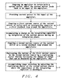
- We now describe the method of the preferred embodiment of the present invention of providing an adjustable integrator using a single capacitor:
- a)
Block 1 couples an amplifier in series with a current mirror, where the current mirror feeds back to an input of the amplifier; - b)
Block 2 provides current pulses to the input of the amplifier; - c)
Block 3 couples a first current source of the current mirror in series with an integrating capacitor as a first feedback loop around the amplifier; - d)
Block 4 accumulates a charge on the integrating capacitor by integration of the current pulses during an integration phase; - e)
Block 5 couples a second current source of the current mirror as a second feedback loop around the amplifier; - f)
Block 6 replicates the current of the first current source in the second current source by a replicating factor thereby increasing the amount of charge that can be measured by the amplifier; and - g)
Block 7 accomplishes range switching by adjusting the replication factor of the second current source where the capacitance of the integrating capacitor is unchanged. - Advantages of the present invention are:
- 1. Only one external capacitor is needed;
- 2. Only two pads for connecting one external capacitor are needed;
- 3. An additional current, fed back to the input of the amplifier, can be used to increase the input range of the charge that can be measured.
- While the invention has been particularly shown and described with reference to the preferred embodiments thereof, it will be understood by those skilled in the art that various changes in form and details may be made without departing from the spirit and scope of the invention.
Claims (16)
- An adjustable integrator, comprising:- an amplifier having an input and an output, where a signal applied at said input of said amplifier provides an amplified signal at said output;- a first feedback loop coupled between said output and said input, said first feedback loop comprising a capacitor, where said first feedback loop provides a first current for placing a charge on said capacitor, said capacitor thereby providing integration of said first current;- a second feedback loop coupled between said output and said input, said second feedback loop providing a mirrored current of said first current and fed back to said input to increase the input range of said charge.
- The adjustable integrator of claim 1, wherein said first current is derived from a first current source.
- The adjustable integrator of claim 2, wherein said mirrored current mirrors said first current by a replication factor 1:m.
- The adjustable integrator of claim 3, wherein said replication factor 1:m is adjustable.
- The adjustable integrator of claim 1, wherein a load device for generating a bias current, is coupled to an output of said first current source to provide an active load for said first feedback loop.
- The adjustable integrator of claim 5, wherein said load device is switched OFF during an integration phase.
- An adjustable integrator, comprising:- an amplifier having an input and an output, where a signal applied at said input of said amplifier provides an amplified signal at said output;- an output stage with an input and a first and a second output, said input of said output stage coupled to said output of said amplifier, said output stage comprising a current mirror which feeds back to said input of said amplifier a replication of an output current of said amplifier, said output stage further comprising:- a first feedback loop comprising in series a first current source of said current mirror and a capacitor, where said first current source, at said first output of said output stage, provides a first current for placing a charge on said capacitor, said capacitor thereby providing integration of said first current; and- a second feedback loop comprising a second current source of said current mirror which mirrors said first current source by a replication factor 1:m, where said second current source, at said second output of said output stage, provides a second current fed back to said input of said amplifier thereby increasing the input range of said charge; anda load device for generating a bias current, coupled to said first current source, at said first output of said output stage, to provide an active load for said first feedback loop.
- The adjustable integrator of claim 7, wherein the replication factor 1:m of said second current source is adjustable.
- The adjustable integrator of claim 7, wherein a switch is coupled in series with said first current source, at said first output of said output stage, and said load device.
- The adjustable integrator of claim 9, wherein said switch may be a transistor, in discrete form or an integrated circuit, or a transistor circuit, in discrete form or an integrated circuit, or a relay, or a mechanical switch.
- The adjustable integrator of claim 7, wherein said load device is switched OFF during an integration phase to prevent a DC offset in said first and second current source.
- The adjustable integrator of claim 5 or 7, wherein said load device is switched ON during a reset phase.
- The adjustable integrator of claim 1 or 7, wherein said capacitor is a discrete or an integrated capacitor.
- A method of creating an adjustable integrator using a single capacitor, comprising the steps of:a) coupling an amplifier in series with a current mirror, where said current mirror feeds back to an input of said amplifier;b) providing current pulses to said input of said amplifier;c) coupling a first current source of said current mirror in series with an integrating capacitor as a first feedback loop around said amplifier;d) accumulating a charge on said integrating capacitor by integration of said current pulses during an integration phase;e) coupling a second current source of said current mirror as a second feedback loop around said amplifier;f) replicating the current of the first current source in the second current source by a replicating factor thereby increasing the amount of charge that can be measured by said amplifier ; andg) accomplishing range switching by adjusting the replication factor of the second current source where the capacitance of said integrating capacitor stays is unchanged.
- The method of claim 14, wherein a load device is coupled to the output of said first current source to provide an active load for said first current source.
- The method of claim 14, wherein a DC offset in the currents of said first and second current sources is avoided by switching off said active load during the integration phase.
Priority Applications (2)
| Application Number | Priority Date | Filing Date | Title |
|---|---|---|---|
| EP08368021A EP2200176A1 (en) | 2008-12-19 | 2008-12-19 | Adjustable integrator using a single capacitance |
| JP2009287476A JP2010148111A (en) | 2008-12-19 | 2009-12-18 | Adjustable integrator using single capacitor |
Applications Claiming Priority (1)
| Application Number | Priority Date | Filing Date | Title |
|---|---|---|---|
| EP08368021A EP2200176A1 (en) | 2008-12-19 | 2008-12-19 | Adjustable integrator using a single capacitance |
Publications (1)
| Publication Number | Publication Date |
|---|---|
| EP2200176A1 true EP2200176A1 (en) | 2010-06-23 |
Family
ID=40589855
Family Applications (1)
| Application Number | Title | Priority Date | Filing Date |
|---|---|---|---|
| EP08368021A Withdrawn EP2200176A1 (en) | 2008-12-19 | 2008-12-19 | Adjustable integrator using a single capacitance |
Country Status (2)
| Country | Link |
|---|---|
| EP (1) | EP2200176A1 (en) |
| JP (1) | JP2010148111A (en) |
Cited By (2)
| Publication number | Priority date | Publication date | Assignee | Title |
|---|---|---|---|---|
| US7830197B2 (en) | 2008-12-22 | 2010-11-09 | Dialog Semiconductor Gmbh | Adjustable integrator using a single capacitance |
| EP2804313A1 (en) * | 2013-05-17 | 2014-11-19 | Nxp B.V. | Transconductance amplifier |
Citations (7)
| Publication number | Priority date | Publication date | Assignee | Title |
|---|---|---|---|---|
| US4059812A (en) | 1976-11-22 | 1977-11-22 | Control Data Corporation | Synchronous pulse generator including flywheel tank circuit with phase locked loop |
| US4251743A (en) * | 1977-10-28 | 1981-02-17 | Nippon Electric Co., Ltd. | Current source circuit |
| EP0944246A2 (en) * | 1998-03-18 | 1999-09-22 | Nec Corporation | Clamp circuit |
| US20030058039A1 (en) * | 2001-09-27 | 2003-03-27 | Masao Noro | Self-operating PWM amplifier |
| US6608516B1 (en) | 2002-01-30 | 2003-08-19 | National Instruments Corporation | Adjustable time constant integrator |
| US20050179468A1 (en) * | 2004-02-17 | 2005-08-18 | Binling Zhou | Implementation of MOS capacitor in CT scanner data acquisition system |
| US20070229161A1 (en) | 2006-04-04 | 2007-10-04 | Dialog Semiconductor, Gmbh | Voltage-to-current converter |
-
2008
- 2008-12-19 EP EP08368021A patent/EP2200176A1/en not_active Withdrawn
-
2009
- 2009-12-18 JP JP2009287476A patent/JP2010148111A/en active Pending
Patent Citations (7)
| Publication number | Priority date | Publication date | Assignee | Title |
|---|---|---|---|---|
| US4059812A (en) | 1976-11-22 | 1977-11-22 | Control Data Corporation | Synchronous pulse generator including flywheel tank circuit with phase locked loop |
| US4251743A (en) * | 1977-10-28 | 1981-02-17 | Nippon Electric Co., Ltd. | Current source circuit |
| EP0944246A2 (en) * | 1998-03-18 | 1999-09-22 | Nec Corporation | Clamp circuit |
| US20030058039A1 (en) * | 2001-09-27 | 2003-03-27 | Masao Noro | Self-operating PWM amplifier |
| US6608516B1 (en) | 2002-01-30 | 2003-08-19 | National Instruments Corporation | Adjustable time constant integrator |
| US20050179468A1 (en) * | 2004-02-17 | 2005-08-18 | Binling Zhou | Implementation of MOS capacitor in CT scanner data acquisition system |
| US20070229161A1 (en) | 2006-04-04 | 2007-10-04 | Dialog Semiconductor, Gmbh | Voltage-to-current converter |
Cited By (3)
| Publication number | Priority date | Publication date | Assignee | Title |
|---|---|---|---|---|
| US7830197B2 (en) | 2008-12-22 | 2010-11-09 | Dialog Semiconductor Gmbh | Adjustable integrator using a single capacitance |
| EP2804313A1 (en) * | 2013-05-17 | 2014-11-19 | Nxp B.V. | Transconductance amplifier |
| US9276535B2 (en) | 2013-05-17 | 2016-03-01 | Nxp B.V. | Transconductance amplifier |
Also Published As
| Publication number | Publication date |
|---|---|
| JP2010148111A (en) | 2010-07-01 |
Similar Documents
| Publication | Publication Date | Title |
|---|---|---|
| KR100733439B1 (en) | A constant-voltage circuit | |
| JP7004585B2 (en) | Current detection method for semiconductor devices, load drive systems and inductor currents | |
| DE102019119875B4 (en) | OUTPUT CURRENT MEASUREMENT FOR A DC/DC CONVERTER WITH EXTERNAL POWER STAGE | |
| KR101719852B1 (en) | Digital Charge Amplifier and Method for Converting Charge Signals into Digital Signals | |
| EP0707381B1 (en) | Circuit and method for generating a clock signal | |
| EP0911978B1 (en) | Generation of temperature compensated low noise symmetrical reference voltages | |
| US8736354B2 (en) | Electronic device and method providing a voltage reference | |
| EP2846212A1 (en) | Circuit to reduce output capacitor of LDOs | |
| US20250279712A1 (en) | Rdson-based current sensing system | |
| US8269550B2 (en) | Temperature and process driven reference | |
| JPS6331206A (en) | Charge amplifying circuit | |
| KR950014094B1 (en) | Sampled Analog Electrical Signal Processing Method and Apparatus | |
| US4396890A (en) | Variable gain amplifier | |
| EP1282131A3 (en) | Reference generator circuit and method for nonvolatile memory devices | |
| US7830197B2 (en) | Adjustable integrator using a single capacitance | |
| US7863908B2 (en) | Current measurement based on a charge in a capacitor | |
| US7265616B2 (en) | Charge amplifier | |
| US20030228024A1 (en) | Shock sound prevention circuit | |
| US7248105B2 (en) | Method and circuit for input offset correction in an amplifier circuit | |
| US20040263243A1 (en) | BTL amplifier capable of providing stability of offset compensation | |
| US6977510B1 (en) | Very precise resistance measurement | |
| JP2010148111A (en) | Adjustable integrator using single capacitor | |
| US6335657B1 (en) | MOSFET amplifier circuit | |
| US20060097806A1 (en) | Wideband Gaussian White Noise Source | |
| CN115248342B (en) | A current sampling circuit, a sampling method and an integrated circuit using the same |
Legal Events
| Date | Code | Title | Description |
|---|---|---|---|
| PUAI | Public reference made under article 153(3) epc to a published international application that has entered the european phase |
Free format text: ORIGINAL CODE: 0009012 |
|
| AK | Designated contracting states |
Kind code of ref document: A1 Designated state(s): AT BE BG CH CY CZ DE DK EE ES FI FR GB GR HR HU IE IS IT LI LT LU LV MC MT NL NO PL PT RO SE SI SK TR |
|
| AX | Request for extension of the european patent |
Extension state: AL BA MK RS |
|
| 17P | Request for examination filed |
Effective date: 20101223 |
|
| AKX | Designation fees paid |
Designated state(s): AT BE BG CH CY CZ DE DK EE ES FI FR GB GR HR HU IE IS IT LI LT LU LV MC MT NL NO PL PT RO SE SI SK TR |
|
| 17Q | First examination report despatched |
Effective date: 20110520 |
|
| STAA | Information on the status of an ep patent application or granted ep patent |
Free format text: STATUS: THE APPLICATION IS DEEMED TO BE WITHDRAWN |
|
| 18D | Application deemed to be withdrawn |
Effective date: 20160203 |