EP2197113A2 - Controlled current source - Google Patents
Controlled current source Download PDFInfo
- Publication number
- EP2197113A2 EP2197113A2 EP09177772A EP09177772A EP2197113A2 EP 2197113 A2 EP2197113 A2 EP 2197113A2 EP 09177772 A EP09177772 A EP 09177772A EP 09177772 A EP09177772 A EP 09177772A EP 2197113 A2 EP2197113 A2 EP 2197113A2
- Authority
- EP
- European Patent Office
- Prior art keywords
- current
- current source
- switching
- transistor
- transistors
- Prior art date
- Legal status (The legal status is an assumption and is not a legal conclusion. Google has not performed a legal analysis and makes no representation as to the accuracy of the status listed.)
- Granted
Links
- 239000003990 capacitor Substances 0.000 description 4
- 230000005669 field effect Effects 0.000 description 4
- 230000001419 dependent effect Effects 0.000 description 3
- 238000010586 diagram Methods 0.000 description 2
- 230000001105 regulatory effect Effects 0.000 description 1
- 239000004065 semiconductor Substances 0.000 description 1
Images



Classifications
-
- H—ELECTRICITY
- H03—ELECTRONIC CIRCUITRY
- H03K—PULSE TECHNIQUE
- H03K17/00—Electronic switching or gating, i.e. not by contact-making and –breaking
- H03K17/16—Modifications for eliminating interference voltages or currents
- H03K17/161—Modifications for eliminating interference voltages or currents in field-effect transistor switches
- H03K17/165—Modifications for eliminating interference voltages or currents in field-effect transistor switches by feedback from the output circuit to the control circuit
Definitions
- the present invention is related to a controlled current source.
- Controlled current sources are known from US 5,111,205 and WO 2006/120246 .
- Current sources in integrated devices provide the required supply current and supply voltage to a plurality of sub-circuits, those sub-circuits providing different functions for the integrated device.
- mobile or handheld devices require different supply voltages for their sub-circuits. Consequently, a DC supply voltage provided, for example, by a battery has to be converted into different supply voltage required by the sub-circuits.
- charge pumps for converting a first voltage into a second output voltage.
- the second output voltage can be higher than the first voltage, at which the charge pump is also referred to as voltage up-converter.
- Those charge pumps are connected to current sources providing the required current to the sub-circuits.
- the charge pump comprises a reservoir capacitor, which may produce ripples across the output signal of the charge pump. It is therefore necessary that the current source must provide power supply ripple rejection (PSRR) means to prevent incorrect operation of sub-circuits connected to those current sources. Since the charge pump switching frequencies are relatively high, the power supply ripple rejection has to be achieved at such high frequencies.
- PSRR power supply ripple rejection
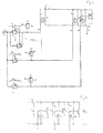
- FIG. 7 shows a controlled current source according to the state of the art known to the inventor.
- the current source 10a comprises a control input 11 at which a control signal Vg1 is being applied. That control signal is derived by a comparison between a reference signal Iref and a feedback signal Ifb.
- the feedback signal is provided by a current sensing path comprising two transistors M4, M8 connected in series. Transistor M4 is part of a current mirror mirroring the sensed current Is to an output current 13.
- ripples due to the switching frequencies of the charge pump connected to the current source 10a may become quite high and distort the overall output signal Io as illustrated in curve C1 of FIG. 6 .
- a main aspect of the present invention is related to the improvement of matching of the output signal Vd and control reference signal Vr. This is achieved by improving the matching of the signal phases applied to several switching and controlled transistors of the current source. Particularly, RC time constants including the gate to source capacitances of the switching transistors within the current source are equalized while at the same time the AC components of the supply signal provided to the current source are mirrored into the output current.
- a controlled current source may comprise a supply source, providing a supply signal having a DC and an AC component and an adjustable current source.
- the current source is coupled to the supply source and comprises switching transistors and switching devices coupled to the transistors to provide an output signal in response to an adjustment word and a control signal.
- the controlled current source further includes control means with a feedback circuit for providing the control signal based on signal provided by sensing means for sensing the DC and the AC component of the supply signal. Means for mirroring mirror the AC component in the supply signal and means for equalizing are provided to match the sensing means to the switching transistors and switching devices of the adjustable current source.
- the means for equalizing comprise at least one of a resistive element and a dummy transistor to match an RC time constant of the sensing means to an RC time constant of the switching transistors and switching devices.
- the means may also comprise a current path to provide a control current, said current path arranged between the supply source and the means for mirroring.
- the adjustable current source may comprise a plurality of switching transistors arranged between the supply source and a current output terminal as well as a plurality of switching devices.
- the switching devices are adapted to be switched in response to the adjustment word.
- Each switching device is arranged between a respective gate of the plurality of switching transistors and a control signal terminal at which the control signal may be applied.
- the resistance of the switching devices and the gate-source capacitance of the respective switching transistors connected thereto are adjusted such that the RC time constants given by the each of the plurality of switching devices and the respective switching transistor connected thereto are substantially equal.
- a controlled current source comprises an adjustable current source having a supply input terminal and an adjustment terminal. At the adjustment terminal, an adjustment word can be applied to adjust an output current provided by the current source.
- the current source comprises a plurality of switching transistors arranged between the supply input terminal and a current output terminal.
- the current source further comprises a plurality of switching devices to be switched in response to the adjustment word. Each switching device of the plurality of switching devices is arranged between a gate of each of the plurality of switching transistors and a control signal terminal.
- the controlled current source comprises a control circuit having a first current sensing path coupled to the supply input terminal to sense an AC portion of a supply signal and coupled to a current mirror to mirror said AC portion to the output current.
- the first current sensing path may comprise a control transistor and a resistive element arranged between a gate of the control transistor and the control signal terminal.
- the additional resistive element connected to the gate of the control transistor allows to adjust the RC time constant given by the product of the resistive value and the gate-source capacitance of the control transistor to be substantially equal to the RC time constant of the resistive value of one of the switching devices and the gate-source capacitance of the respective switching transistor connected thereto.
- the path resistance-capacitance given by the gate to source capacitance of the respective switching transistors and the switching devices connected thereto are substantially equal. Consequently, any AC signal component coupled into the control signal terminal has substantially the same phase. AC matching is therefore improved.
- At least one of the switching devices of the plurality of switching devices comprises a first switch and at least a second switch arranged parallel or series to the first switch. Since each switch comprises a specific resistance, arranging a plurality of switches in parallel to each other receiving the same component of the adjustment word reduces the overall resistance of the switching device.
- the additional switches arranged in parallel can be used to equalize the RC constant given by the product of the resistive value and the gate-source capacitance of the switching transistor connected thereto to the RC time constant given by the product of the resistance and the capacitance of a second switching path.
- the current source may comprise at least one floating dummy transistor, said at least one floating dummy transistor coupled with its gate to the gate of the switching transistor of the plurality of switching transistors.
- the at least one floating dummy transistor and said switching transistor may comprise substantially the same size.
- the dummy transistor may have different geometric dimensions compared to the switching transistors connected to the dummy transistor.
- the drain terminal of the dummy transistor may be floating.
- the additional dummy transistor adjusts the gate-source capacitance of the switching transistor, thereby equalizing, as already explained above, the RC time constant given by the product of the resistance of the switching device and the gate-source capacitance of the switching transistor to respective other switching devices and switching transistors connected thereto.
- Two adjacent switching transistors may comprise geometric dimensions or geometric size which differs by a factor of two.
- control circuit comprises a second current sensing path having a sensing transistor arranged in parallel to the sensing transistor of the first current sensing path.
- the sensing transistors of both current sensing paths may comprise the same geometric proportions and/or substantially the same gate to source capacitances.
- the first current sensing path may be used to provide the DC portion.
- the gate terminal of the sensing transistor of the first and second current path may be coupled via a switching device to a reference current source.
- the first current sensing path may also comprise a second reference source.
- the current sensed by the current sensing transistor of the second current sensing path may be regulated close to the difference of the reference currents of the first and second reference current sources.
- the gate-source capacitance of the sensing transistors of both current sensing paths may be selected such that they are equal to 2 k times the gate-source capacitance of one of the switching transistors, wherein k is an integer.
- the controlled current source may comprise in a further embodiment a dummy transistor.
- the gate of the dummy transistor is coupled to the gate of the sensing transistor of the first current sensing path.
- the size of the dummy transistor may be selected to satisfy the above-mentioned condition. Further, the dummy transistor may be floating.
- circuits or elements are represented enlarged with respect to other elements. Such enlargement is for illustration purposes and does not reflect differences in real size when implementing those elements.
- the circuits and sub-circuits shown herein can be implemented in a single semiconductor body as an integrated circuit or as separated circuits using integrated as well as discrete components and devices.
- FIG. 1A illustrates an embodiment of a controlled current source including a charge pump arrangement.
- Charge pump arrangement 1 comprises a clock input terminal for clock signal CLK and a supply terminal Vsup.
- the clocked charge pump is operated in two successive periods of a cycle of signal CLK. In a first period of clock signal CLK, one or more capacitors are charged using the externally applied supply voltage Vsup. In a second period of clock signal CLK applied to clock input terminal, the charge stored in the capacitors is provided at an output terminal.
- the output voltage provided at the output of the charge pump can be higher than the externally applied supply voltage Vsup.
- the controlled current source connected to the output terminal of charge pump 1 draws the charge provided at the output of the charge pump continuously.
- charge pump 1 may have to operate continuously, thereby producing ripples on its provided output voltage.
- the output voltage is dependent on the load connected to the controlled current source.
- the ripples may be in the range of 100 mV at 4 V output voltage and 100 mA current drawn from the output voltage.
- the controlled current source comprises a current source 10 with supply terminal 13 connected to charge pump 1 and an output terminal 12 at which a controlled output voltage Vd is provided.
- the output voltage Vd is dependent on the load connected to the output terminal 12.
- a control circuit 2 of the controlled current source is connected to output terminal 12 of current source 10 as well as to a control signal terminal 11 of the current source.
- the control circuit 2 uses two current sensing paths Is1 and Is2 to sense the AC and DC portion of the current provided by current source 10. Due to some AC component in the supply voltage provided by charge pump 1, the voltages applied to gates of switching transistors within current source 10 may be different due to finite switch resistances of switches and gate-source capacitance of the switching transistors.
- the control circuit now senses the AC component and provides a respective control signal to the current source.
- FIG. 1B shows a more detailed view of the controlled current source according to the present invention.
- the current source 10 comprises a supply terminal 13 at which the supply voltage from the charge pump (not shown) is received.
- Output terminal 12 providing the load voltage Vd is connected to load 40.
- the current source comprises a control signal terminal 11.
- control circuit 2 comprises a first current path 16 as well as a second current path 15, both current paths sensing a current flowing through current source 10.
- the second current sensing path 15 comprises a current sensing transistor (not shown herein) as well as two field-effect transistors M4 and M8 forming a series circuit.
- the current sensing provides the sensing current Is.
- the gate voltage Vg1 is controlled in such a way that the current through the sensing transistor of the second sensing path 15 satisfies the equation. This is achieved by comparing the current Is at terminal Ifb of comparator 30 with a reference current at terminal Iref.
- the first current path 16 comprises transistors M5 and M9 connected in series with a current sensing transistor in the current source 10 (not shown) of the first current sensing path 16.
- the gate terminals of transistors M5 and M9 are connected to the respective gate terminals of transistors M4 and M8 of the second current sensing path 15.
- the sensed current Is1 is used to determine currents Ib3 and Ib4 of paths 17 and 18.
- Path 17 includes diode M7 and a further field-effect transistor M10 which represents the current mirror transistor to mirror the AC component of M10 to transistors M8 and M9 of current sensing paths 15 and 16, respectively.
- Diode M7 is also coupled to output terminal 12 of the current source.
- a second current path 18 with the reference current Ib3 comprises transistor M6 as well as a further transistor M3 (not shown herein), said transistor being part of current source 10.
- the transistor M3 provides current 13, being substantially equal to reference currents Ib3 and Ib4.
- the AC component of the second path 18 is coupled via current mirror transistor M6 into transistors M4 and M5, respectively.
- the transistors M4 and M6 carry the same proportion of AC and DC signal components.
- Such structure is one aspect to improve the AC matching of the controlled current source according to the current invention.
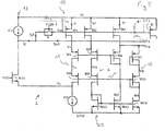
- FIG. 2 now illustrates a new switching arrangement of the current source to obtain equal gate voltages at the respective gates of the switching transistors.
- the current source comprises a plurality of switching transistors MP 1 to MP n being arranged in parallel between supply input terminal 13 and output terminal 12.
- the transistors MP 1 to MP n each comprise a specified width/length ratio.
- each transistor MP k of the transistors MP 1 to MP n comprise the width/length ratio satisfying the term (width/length * 2 k-1 ). Therefore, transistor MP 1 has half the ratio compared to transistor MP 2 and so forth.
- each gate of the respective switching transistors and the supply terminal 13 a gate-source capacitance given by Cg 1 to Cg n can be specified.
- the gate terminals of each transistor MP 1 to MP n are connected to respective switching devices 100 1 , 100 2 to 100 n .
- Switching device 100 1 comprises a single switch arranged between control terminal 11 and the respective gate of the first switching transistor MP 1 . Further, a node between switch S 1 of switching device 100 1 and gate of switching transistor MP 1 is connected to an additional switch xs1 being coupled to the supply potential Vs.
- either switch s1 or switch xs1 of each switching device is closed while the other one is open.
- each switching transistor of the switching devices 100 1 to 100 n is either activated or deactivated in response to the adjustment word D.
- the second switching device 100 2 comprises two switches s1 arranged in parallel. Each switch is closed or opened by the respective adjustment component d 2 of adjustment word D. Accordingly, switching device 100 n comprises n switches S1 arranged in parallel.
- Each switch of the switching devices 100 1 to 100 n comprises a resistance R 1 , R 2 to R n .
- the parallel arrangement of additional switches keeps the RC time constant of path resistance and gate-source capacitance equal to each other. For instance, product R 1 * Cg 1 equals R 2 * Cg 2 due to the fact that the second switching transistor MP 2 has twice the capacitance of the first switching transistor but R 2 is half the resistance of R 1 .
- the AC components g 1 , to g n at the gates of the switching transistors MP 1 to MP n are substantially equal to each other.
- FIG. 4 shows an arrangement also improving the matching of the AC voltage components g 1 to g n .
- an additional dummy transistor MP 1d is provided, said dummy transistor having a floating drain terminal.
- the dimensions of the dummy transistor are set equal to the dimension of the first switching transistor MP 1 .
- the gate of the dummy transistor MP 1d is connected to the gate of the first switching transistor MP 1 .
- the overall gate-source capacitance of the first switching transistor and the first dummy switching transistor equals the second switching transistor.
- gate-source capacitance represents the capacitance between the gate and the source terminal. Consequently, the resistance R 1 of the first switching device and R 2 of the second switching device can be equalized as well.
- the last switching transistor MP n is connected with its gate to a switching device 100 n comprising n-1 switches arranged in parallel.
- a plurality of dummy transistors MP 1d , MP 2d and MP 3d are connected to respective switching transistors MP 1 , MP 2 and MP 3 .
- the respective drain terminals of each dummy transistor are floating.
- FIG. 5 shows an embodiment of a new regulation circuit according to the proposed current source.
- the regulation circuit comprises four current paths 15, 16, 17 and 18, each of them having a plurality of transistors connected in series.
- a first current sensing path 16 comprises a sensing transistor M2 as well as two transistors M5 and M9 connected in series and coupled to a current mirror transistor M12 of a current mirror 20.
- Current mirror transistor 12 of current mirror 20 mirrors the current into transistors M13 and M14 of respective current paths 17 and 18.
- a second current sensing path 15 comprises sensing transistor M1 as well two transistors M4 and M8 connected in series and coupled to a reference current source Ib2.
- the gates of sensing transistors M1 and M2 are coupled to the gate of a third current transistor M3 providing the current for paths 17 and 18.
- the gates of transistors M1, M2 and M3 are connected to a gate of a dummy transistor D and a switch S1. The purpose of dummy transistor D will be explained later in greater detail.
- the voltage Vg1 applied to the gates of the respective transistors are provided by the comparator 30 as shown in FIG. 1B .
- a current source Ib1 is arranged between supply terminal 13 providing the supply voltage Vs and transistor M11.
- the gate of transistor M11 receives the bias voltage Vb2 and its drain is connected to the current source Ib2 of the second current sensing path 15.
- a node between the reference current source Ib1 and the bias transistor M11 is connected to terminal 11 to provide the control voltage Vg.
- Said control voltage Vg is applied to terminal 11a of the circuits shown in Figures 2 and 3 .
- Switch Rs1 connected to the gates of the respective current transistors M1, M2, M3 and the dummy transistor D is also coupled to said node.
- the sensed current Is1 is used to define via current mirror transistor M12 the reference currents Ib3 and Ib4 of the current paths 17 and 18. Due to the fact that a sense current Is1 is proportional to the sense current Is of the second current path, the reference currents Ib3 and Ib4 will carry proportionate DC and AC components.
- the size of current sensing transistors M1 and particularly of M2 is equal to the size of switching transistor MP 1 .
- Transistors M6 and M7 of current paths 17 and 18 are connected with their respective gates to their respective drain terminals, thereby forming a diode. Accordingly, the voltage drop over transistors M6 and M7 comprise an AC as well as a DC component. The AC component of transistor M6 is now mirrored to transistors M4 and M5 of the second and first current sensing paths, respectively.
- the output voltage Vd is defined by a load connected thereto.
- the current drawn by the load is substantially provided by switching transistors MP 1 to MP n of the current source portion shown in Figures 2 and 3 .
- the current paths 17 and 18 will draw a current which is provided by the transistor M3. Therefore, the current 13 is similar to the current flowing through transistors M6 and M7 of current paths 17 and 18.
- Current 13 may also be a little bit smaller than the current through M6 and M7 wherein the remaining current is provided by the switching transistors MP.
- I ⁇ 3 I ⁇ b ⁇ 3 + I ⁇ b ⁇ 4 + ⁇ s ⁇ o ⁇ m ⁇ e s ⁇ m ⁇ a ⁇ l ⁇ l r ⁇ e ⁇ s ⁇ t p ⁇ r ⁇ o ⁇ v ⁇ i ⁇ d ⁇ e ⁇ d b ⁇ y t ⁇ r ⁇ a ⁇ n ⁇ s ⁇ i ⁇ s ⁇ t ⁇ o ⁇ r ⁇ s M ⁇ P ⁇
- the voltage Vr of the second current sensing path equals the output voltage Vd.
- the DC component of current Ig is substantially zero, because there are no currents flowing through the gates of the switching transistors as well as of the current sensing transistors.
- the AC component of current Ig is non-zero if the supply voltage Vs comprises an AC component, e.g. some ripples. Accordingly, the AC component in current Ig adds to the AC component of Is and Is1 leading to a ripple in sense current Is.
- a switch Rs1 is connected in series to the gates of the current sensing transistors M1, M2 as well as of transistor M3 and D. Although in this embodiment, only a single switch Rs1 is shown, it may be required to connect several switches in parallel or in series.
- the purpose of the switch RS1 is to equalize the RC time constants of the current (sensing) transistors M1, M2, M3 and D with the switching transistors and the switches connected thereto.
- the multiplication product of the path resistance between the gate-source capacitance of current sensing transistors M1 or M2 and the resistance of the switching device Rs1 connected to those gates should be equal to the multiplication product of the resistance of the switching device connected to the first switching transistor and the respective gate-source capacitance of the first switching transistor.
- the gate-source capacitance of transistors M1, M2, M3 and the dummy transistor D together is selected such that it is equal to 2 k times the gate-source capacitance of the first switching transistor MP 1 , wherein k is a positive integer.
- the AC component of voltage Vg1 and the voltages of the gates at the switching transistors MP 1 to MP n are all maintained the same.
- the accuracy of the feedback current Is is improved and the regulation circuit regulates the current Is close to the reference current Ib3 - Ib1. This will reduce the overall ripple in the output current 10 drawn by the load.
- FIG. 6 shows a time current diagram illustrating the AC ripples in the output current.
- Curve C1 shows the output current including some ripples without any AC component matching.
- the second curve C2 illustrates the output current if the gate-source capacitance of the respective switching transistors and the switching devices connected thereto are matched. As one can see, a small improvement is already achieved.
- curve C3 shows the output current of a current source according to the proposed embodiments including the resistance and gate-source capacitance matching of the transistors in the control circuit, the switching transistors as well as the additional current mirroring of the AC component to the output current.
- the present invention proposes to improve the AC matching using weighted resistance switches or weighted gate-source capacitance to equalize the time constant between the several switching transistors and switches connected to the respective gates. Further, an additional sense current is used to improve the drain voltage matching.
Landscapes
- Dc-Dc Converters (AREA)
- Power Conversion In General (AREA)
- Static Random-Access Memory (AREA)
- Electronic Switches (AREA)
Abstract
Description
- The present invention is related to a controlled current source.
- Controlled current sources are known from
US 5,111,205 andWO 2006/120246 . Current sources in integrated devices provide the required supply current and supply voltage to a plurality of sub-circuits, those sub-circuits providing different functions for the integrated device. Particularly, mobile or handheld devices require different supply voltages for their sub-circuits. Consequently, a DC supply voltage provided, for example, by a battery has to be converted into different supply voltage required by the sub-circuits. - It is common practice to use charge pumps for converting a first voltage into a second output voltage. The second output voltage can be higher than the first voltage, at which the charge pump is also referred to as voltage up-converter. Those charge pumps are connected to current sources providing the required current to the sub-circuits. In such cases, the charge pump comprises a reservoir capacitor, which may produce ripples across the output signal of the charge pump. It is therefore necessary that the current source must provide power supply ripple rejection (PSRR) means to prevent incorrect operation of sub-circuits connected to those current sources. Since the charge pump switching frequencies are relatively high, the power supply ripple rejection has to be achieved at such high frequencies.
-
FIG. 7 shows a controlled current source according to the state of the art known to the inventor. The current source 10a comprises acontrol input 11 at which a control signal Vg1 is being applied. That control signal is derived by a comparison between a reference signal Iref and a feedback signal Ifb. The feedback signal is provided by a current sensing path comprising two transistors M4, M8 connected in series. Transistor M4 is part of a current mirror mirroring the sensed current Is to anoutput current 13. - Due to the presence of an AC component in the sensed current Is, the voltage signals Vr and the voltage output signal Vd defined by the load connected thereto are different. Further, the AC component of the current through the transistors M4 and M6 are different because no AC component is flowing through transistor M6. The current through the load is now given by internal switching transistors of the current source 10a, while the current in M6 and M7 is defined by Ib3 and Ib4.
- Nevertheless, ripples due to the switching frequencies of the charge pump connected to the current source 10a may become quite high and distort the overall output signal Io as illustrated in curve C1 of
FIG. 6 . - It is therefore desirable to provide an improved controlled current source with reduced power supply ripples.
- This and other objectives of the present invention are solved by
independent claim 1. Further embodiments and advantages of the present invention are presented in the dependent claims. A main aspect of the present invention is related to the improvement of matching of the output signal Vd and control reference signal Vr. This is achieved by improving the matching of the signal phases applied to several switching and controlled transistors of the current source. Particularly, RC time constants including the gate to source capacitances of the switching transistors within the current source are equalized while at the same time the AC components of the supply signal provided to the current source are mirrored into the output current. - In an embodiment a controlled current source may comprise a supply source, providing a supply signal having a DC and an AC component and an adjustable current source. The current source is coupled to the supply source and comprises switching transistors and switching devices coupled to the transistors to provide an output signal in response to an adjustment word and a control signal. The controlled current source further includes control means with a feedback circuit for providing the control signal based on signal provided by sensing means for sensing the DC and the AC component of the supply signal. Means for mirroring mirror the AC component in the supply signal and means for equalizing are provided to match the sensing means to the switching transistors and switching devices of the adjustable current source.
- In an embodiment the means for equalizing comprise at least one of a resistive element and a dummy transistor to match an RC time constant of the sensing means to an RC time constant of the switching transistors and switching devices. The means may also comprise a current path to provide a control current, said current path arranged between the supply source and the means for mirroring.
- The adjustable current source may comprise a plurality of switching transistors arranged between the supply source and a current output terminal as well as a plurality of switching devices. The switching devices are adapted to be switched in response to the adjustment word. Each switching device is arranged between a respective gate of the plurality of switching transistors and a control signal terminal at which the control signal may be applied. The resistance of the switching devices and the gate-source capacitance of the respective switching transistors connected thereto are adjusted such that the RC time constants given by the each of the plurality of switching devices and the respective switching transistor connected thereto are substantially equal.
- In an another embodiment, a controlled current source comprises an adjustable current source having a supply input terminal and an adjustment terminal. At the adjustment terminal, an adjustment word can be applied to adjust an output current provided by the current source. For this purpose, the current source comprises a plurality of switching transistors arranged between the supply input terminal and a current output terminal. The current source further comprises a plurality of switching devices to be switched in response to the adjustment word. Each switching device of the plurality of switching devices is arranged between a gate of each of the plurality of switching transistors and a control signal terminal. Finally, the controlled current source comprises a control circuit having a first current sensing path coupled to the supply input terminal to sense an AC portion of a supply signal and coupled to a current mirror to mirror said AC portion to the output current.
- The first current sensing path may comprise a control transistor and a resistive element arranged between a gate of the control transistor and the control signal terminal. The additional resistive element connected to the gate of the control transistor allows to adjust the RC time constant given by the product of the resistive value and the gate-source capacitance of the control transistor to be substantially equal to the RC time constant of the resistive value of one of the switching devices and the gate-source capacitance of the respective switching transistor connected thereto. In other words, the path resistance-capacitance given by the gate to source capacitance of the respective switching transistors and the switching devices connected thereto are substantially equal. Consequently, any AC signal component coupled into the control signal terminal has substantially the same phase. AC matching is therefore improved.
- In an embodiment, at least one of the switching devices of the plurality of switching devices comprises a first switch and at least a second switch arranged parallel or series to the first switch. Since each switch comprises a specific resistance, arranging a plurality of switches in parallel to each other receiving the same component of the adjustment word reduces the overall resistance of the switching device. The additional switches arranged in parallel can be used to equalize the RC constant given by the product of the resistive value and the gate-source capacitance of the switching transistor connected thereto to the RC time constant given by the product of the resistance and the capacitance of a second switching path.
- Alternately, the current source may comprise at least one floating dummy transistor, said at least one floating dummy transistor coupled with its gate to the gate of the switching transistor of the plurality of switching transistors. The at least one floating dummy transistor and said switching transistor may comprise substantially the same size. Alternately, the dummy transistor may have different geometric dimensions compared to the switching transistors connected to the dummy transistor. The drain terminal of the dummy transistor may be floating.
- The additional dummy transistor adjusts the gate-source capacitance of the switching transistor, thereby equalizing, as already explained above, the RC time constant given by the product of the resistance of the switching device and the gate-source capacitance of the switching transistor to respective other switching devices and switching transistors connected thereto.
- Two adjacent switching transistors may comprise geometric dimensions or geometric size which differs by a factor of two.
- In a further embodiment, the control circuit comprises a second current sensing path having a sensing transistor arranged in parallel to the sensing transistor of the first current sensing path. The sensing transistors of both current sensing paths may comprise the same geometric proportions and/or substantially the same gate to source capacitances.
- While the second current sensing path comprises the current mirror transistor to mirror the AC signal portion of the supply voltage signal to the output current, the first current sensing path may be used to provide the DC portion. The gate terminal of the sensing transistor of the first and second current path may be coupled via a switching device to a reference current source.
- The first current sensing path may also comprise a second reference source. As a result, the current sensed by the current sensing transistor of the second current sensing path may be regulated close to the difference of the reference currents of the first and second reference current sources.
- In addition, the gate-source capacitance of the sensing transistors of both current sensing paths may be selected such that they are equal to 2k times the gate-source capacitance of one of the switching transistors, wherein k is an integer. To satisfy such condition, the controlled current source may comprise in a further embodiment a dummy transistor. The gate of the dummy transistor is coupled to the gate of the sensing transistor of the first current sensing path. The size of the dummy transistor may be selected to satisfy the above-mentioned condition. Further, the dummy transistor may be floating.
- Several embodiments and various aspects of the present invention will be described in greater detail with reference to the accompanying drawings in which
- FIG. 1A
- shows an embodiment of a controlled current source including a charge pump arrangement to provide the respective supply voltage,
- FIG. 1B
- shows an example of a controlled current source ac- cording to the present invention,
- FIG. 2
- shows a schematic of an embodiment of a current source being part of the controlled current source according to the present invention,
- FIG. 3
- shows an alternate embodiment of the current source according to the present invention,
- FIG. 4
- shows a further alternate embodiment of a current source according to the present invention,
- FIG. 5
- shows an embodiment of the control circuit accord- ing to the present invention,
- FIG. 6
- shows a time current diagram to illustrate the ef- fect of improved AC matching according to an em- bodiment of the present invention,
- FIG. 7
- shows a known controlled current source.
- In the following detailed description, several aspects of the present invention are explained in greater detail with reference to the accompanying drawings. However, those features shown in the figures are not restricted to the respective embodiments, but can be combined in different ways by a person skilled in the art. The switches for the current source, the control circuit as well for other sub-circuits of the arrangement according to the present invention are implemented by field-effect transistors for illustration purposes. However, those switches are not restricted to field-effect transistors, but can be implemented in different ways. The clocked charge pump can be implemented in various ways and is therefore not restricted to any exemplary embodiment shown herein.
- Some sub-circuits or elements are represented enlarged with respect to other elements. Such enlargement is for illustration purposes and does not reflect differences in real size when implementing those elements. The circuits and sub-circuits shown herein can be implemented in a single semiconductor body as an integrated circuit or as separated circuits using integrated as well as discrete components and devices.
-
FIG. 1A illustrates an embodiment of a controlled current source including a charge pump arrangement.Charge pump arrangement 1 comprises a clock input terminal for clock signal CLK and a supply terminal Vsup. The clocked charge pump is operated in two successive periods of a cycle of signal CLK. In a first period of clock signal CLK, one or more capacitors are charged using the externally applied supply voltage Vsup. In a second period of clock signal CLK applied to clock input terminal, the charge stored in the capacitors is provided at an output terminal. Depending on the capacitors and the structure ofcharge pump 1, the output voltage provided at the output of the charge pump can be higher than the externally applied supply voltage Vsup. In any case, the controlled current source connected to the output terminal ofcharge pump 1 draws the charge provided at the output of the charge pump continuously. As a consequence,charge pump 1 may have to operate continuously, thereby producing ripples on its provided output voltage. The output voltage is dependent on the load connected to the controlled current source. The ripples may be in the range of 100 mV at 4 V output voltage and 100 mA current drawn from the output voltage. - The controlled current source comprises a
current source 10 withsupply terminal 13 connected to chargepump 1 and anoutput terminal 12 at which a controlled output voltage Vd is provided. The output voltage Vd is dependent on the load connected to theoutput terminal 12. - A
control circuit 2 of the controlled current source is connected tooutput terminal 12 ofcurrent source 10 as well as to acontrol signal terminal 11 of the current source. Thecontrol circuit 2 uses two current sensing paths Is1 and Is2 to sense the AC and DC portion of the current provided bycurrent source 10. Due to some AC component in the supply voltage provided bycharge pump 1, the voltages applied to gates of switching transistors withincurrent source 10 may be different due to finite switch resistances of switches and gate-source capacitance of the switching transistors. The control circuit now senses the AC component and provides a respective control signal to the current source. -
FIG. 1B shows a more detailed view of the controlled current source according to the present invention. Thecurrent source 10 comprises asupply terminal 13 at which the supply voltage from the charge pump (not shown) is received.Output terminal 12 providing the load voltage Vd is connected to load 40. In addition, the current source comprises acontrol signal terminal 11. To match the AC components and improve the charge pump ripple rejection,control circuit 2 comprises a firstcurrent path 16 as well as a secondcurrent path 15, both current paths sensing a current flowing throughcurrent source 10. The secondcurrent sensing path 15 comprises a current sensing transistor (not shown herein) as well as two field-effect transistors M4 and M8 forming a series circuit. - The current sensing provides the sensing current Is. The sensing current transistor is selected such that the sensed current Is satisfies the equation Is = s2/s*ILSB, wherein s2 is the width/length ratio of the current sensing transistor, s is the width/length ratio of one of the switching transistors of
current source 10, explained later in greater detail, and ILSB represents the current through the switching transistor corresponding to the least significant bit of the current source. - The gate voltage Vg1 is controlled in such a way that the current through the sensing transistor of the
second sensing path 15 satisfies the equation. This is achieved by comparing the current Is at terminal Ifb ofcomparator 30 with a reference current at terminal Iref. - The first
current path 16 comprises transistors M5 and M9 connected in series with a current sensing transistor in the current source 10 (not shown) of the firstcurrent sensing path 16. The gate terminals of transistors M5 and M9 are connected to the respective gate terminals of transistors M4 and M8 of the secondcurrent sensing path 15. The sensed current Is1 is used to determine currents Ib3 and Ib4 ofpaths 17 and 18. - Since current Is1 is proportional to current Is of
path 15, reference currents Ib3 and Ib4 will also carry proportionate AC components. Path 17 includes diode M7 and a further field-effect transistor M10 which represents the current mirror transistor to mirror the AC component of M10 to transistors M8 and M9 ofcurrent sensing paths output terminal 12 of the current source. A secondcurrent path 18 with the reference current Ib3 comprises transistor M6 as well as a further transistor M3 (not shown herein), said transistor being part ofcurrent source 10. The transistor M3 provides current 13, being substantially equal to reference currents Ib3 and Ib4. - The AC component of the
second path 18 is coupled via current mirror transistor M6 into transistors M4 and M5, respectively. As a result, the transistors M4 and M6 carry the same proportion of AC and DC signal components. Such structure is one aspect to improve the AC matching of the controlled current source according to the current invention. -
FIG. 2 now illustrates a new switching arrangement of the current source to obtain equal gate voltages at the respective gates of the switching transistors. - The current source comprises a plurality of switching transistors MP1 to MPn being arranged in parallel between
supply input terminal 13 andoutput terminal 12. The transistors MP1 to MPn each comprise a specified width/length ratio. Particularly, each transistor MPk of the transistors MP1 to MPn comprise the width/length ratio satisfying the term (width/length * 2k-1). Therefore, transistor MP1 has half the ratio compared to transistor MP2 and so forth. - Between each gate of the respective switching transistors and the
supply terminal 13, a gate-source capacitance given by Cg1 to Cgn can be specified. The gate terminals of each transistor MP1 to MPn are connected torespective switching devices Switching device 1001 comprises a single switch arranged betweencontrol terminal 11 and the respective gate of the first switching transistor MP1. Further, a node between switch S1 of switchingdevice 1001 and gate of switching transistor MP1 is connected to an additional switch xs1 being coupled to the supply potential Vs. Depending on the adjustment word D having the components d1 to dn, either switch s1 or switch xs1 of each switching device is closed while the other one is open. Accordingly, at gate of the switching transistor MP1, either the voltage Vg from thecontrol terminal 11 or the supply voltage Vs is applied. Consequently, each switching transistor of theswitching devices 1001 to 100n is either activated or deactivated in response to the adjustment word D. Thesecond switching device 1002 comprises two switches s1 arranged in parallel. Each switch is closed or opened by the respective adjustment component d2 of adjustment word D. Accordingly, switchingdevice 100n comprises n switches S1 arranged in parallel. - Each switch of the
switching devices 1001 to 100n comprises a resistance R1, R2 to Rn. The parallel arrangement of additional switches keeps the RC time constant of path resistance and gate-source capacitance equal to each other. For instance, product R1 * Cg1 equals R2 * Cg2 due to the fact that the second switching transistor MP2 has twice the capacitance of the first switching transistor but R2 is half the resistance of R1. In summary, the arrangement equals theequation 
- As an overall result, the AC components g1, to gn at the gates of the switching transistors MP1 to MPn are substantially equal to each other.
- As an alternative embodiment,
FIG. 4 shows an arrangement also improving the matching of the AC voltage components g1 to gn. In this embodiment, an additional dummy transistor MP1d is provided, said dummy transistor having a floating drain terminal. The dimensions of the dummy transistor are set equal to the dimension of the first switching transistor MP1. The gate of the dummy transistor MP1d is connected to the gate of the first switching transistor MP1. - As a result, the overall gate-source capacitance of the first switching transistor and the first dummy switching transistor equals the second switching transistor. In this respect gate-source capacitance represents the capacitance between the gate and the source terminal. Consequently, the resistance R1 of the first switching device and R2 of the second switching device can be equalized as well. In such case, the last switching transistor MPn is connected with its gate to a
switching device 100n comprising n-1 switches arranged in parallel. - In a further embodiment shown in
FIG. 4 , a plurality of dummy transistors MP1d, MP2d and MP3d are connected to respective switching transistors MP1, MP2 and MP3. The respective drain terminals of each dummy transistor are floating. The size of the dummy transistors MP1d to MP3d is selected such that the overall gate-source capacitance of a dummy transistor connected to the respective switching transistor is equal and satisfies the equation Cg1 = Cg2 = Cg3. Consequently, the resistance of theswitches 1001 to 1003 connected to the respective gates of the switching transistors MP1 to MP3 should be selected equal. -
FIG. 5 shows an embodiment of a new regulation circuit according to the proposed current source. - The regulation circuit comprises four
current paths current sensing path 16 comprises a sensing transistor M2 as well as two transistors M5 and M9 connected in series and coupled to a current mirror transistor M12 of acurrent mirror 20.Current mirror transistor 12 ofcurrent mirror 20 mirrors the current into transistors M13 and M14 of respectivecurrent paths 17 and 18. - A second
current sensing path 15 comprises sensing transistor M1 as well two transistors M4 and M8 connected in series and coupled to a reference current source Ib2. The gates of sensing transistors M1 and M2 are coupled to the gate of a third current transistor M3 providing the current forpaths 17 and 18. Finally the gates of transistors M1, M2 and M3 are connected to a gate of a dummy transistor D and a switch S1. The purpose of dummy transistor D will be explained later in greater detail. - The voltage Vg1 applied to the gates of the respective transistors are provided by the
comparator 30 as shown inFIG. 1B . In addition, a current source Ib1 is arranged betweensupply terminal 13 providing the supply voltage Vs and transistor M11. The gate of transistor M11 receives the bias voltage Vb2 and its drain is connected to the current source Ib2 of the secondcurrent sensing path 15. - A node between the reference current source Ib1 and the bias transistor M11 is connected to terminal 11 to provide the control voltage Vg. Said control voltage Vg is applied to terminal 11a of the circuits shown in
Figures 2 and3 . Switch Rs1 connected to the gates of the respective current transistors M1, M2, M3 and the dummy transistor D is also coupled to said node. - In operation of the control circuit, the sensed current Is1 is used to define via current mirror transistor M12 the reference currents Ib3 and Ib4 of the
current paths 17 and 18. Due to the fact that a sense current Is1 is proportional to the sense current Is of the second current path, the reference currents Ib3 and Ib4 will carry proportionate DC and AC components. In an embodiment, the size of current sensing transistors M1 and particularly of M2 is equal to the size of switching transistor MP1. - Transistors M6 and M7 of
current paths 17 and 18 are connected with their respective gates to their respective drain terminals, thereby forming a diode. Accordingly, the voltage drop over transistors M6 and M7 comprise an AC as well as a DC component. The AC component of transistor M6 is now mirrored to transistors M4 and M5 of the second and first current sensing paths, respectively. - The output voltage Vd is defined by a load connected thereto. The current drawn by the load is substantially provided by switching transistors MP1 to MPn of the current source portion shown in
Figures 2 and3 . Still, thecurrent paths 17 and 18 will draw a current which is provided by the transistor M3. Therefore, the current 13 is similar to the current flowing through transistors M6 and M7 ofcurrent paths 17 and 18. Current 13 may also be a little bit smaller than the current through M6 and M7 wherein the remaining current is provided by the switching transistors MP. Current 13 therefore satisfies the equation
- Due to the current mirrors M6 and M10 of
current paths 17 and 18, the voltage Vr of the second current sensing path equals the output voltage Vd. - In operation, the DC component of current Ig is substantially zero, because there are no currents flowing through the gates of the switching transistors as well as of the current sensing transistors. However, the AC component of current Ig is non-zero if the supply voltage Vs comprises an AC component, e.g. some ripples. Accordingly, the AC component in current Ig adds to the AC component of Is and Is1 leading to a ripple in sense current Is.
- To improve the AC component matching of the control circuit as well as of the current source, a switch Rs1 is connected in series to the gates of the current sensing transistors M1, M2 as well as of transistor M3 and D. Although in this embodiment, only a single switch Rs1 is shown, it may be required to connect several switches in parallel or in series. The purpose of the switch RS1 is to equalize the RC time constants of the current (sensing) transistors M1, M2, M3 and D with the switching transistors and the switches connected thereto. The multiplication product of the path resistance between the gate-source capacitance of current sensing transistors M1 or M2 and the resistance of the switching device Rs1 connected to those gates should be equal to the multiplication product of the resistance of the switching device connected to the first switching transistor and the respective gate-source capacitance of the first switching transistor.
- At the same time, the gate-source capacitance of transistors M1, M2, M3 and the dummy transistor D together is selected such that it is equal to 2k times the gate-source capacitance of the first switching transistor MP1, wherein k is a positive integer. In other words,
equation 1 as well asequation 2 is to be satisfied whereinequation 1 is given by
- Wherein RS1 is the resistance of switch Rs1 and CM1 is the gate-source capacitance of Transistor M1.
Equation 2 is given by
- In the above-mentioned condition, the AC component of voltage Vg1 and the voltages of the gates at the switching transistors MP1 to MPn are all maintained the same. The accuracy of the feedback current Is is improved and the regulation circuit regulates the current Is close to the reference current Ib3 - Ib1. This will reduce the overall ripple in the output current 10 drawn by the load.
-
FIG. 6 shows a time current diagram illustrating the AC ripples in the output current. - Curve C1 shows the output current including some ripples without any AC component matching. The second curve C2 illustrates the output current if the gate-source capacitance of the respective switching transistors and the switching devices connected thereto are matched. As one can see, a small improvement is already achieved.
- An even better improvement with only small ripples in the range of roughly 1 mA is illustrated in curve C3. This curve shows the output current of a current source according to the proposed embodiments including the resistance and gate-source capacitance matching of the transistors in the control circuit, the switching transistors as well as the additional current mirroring of the AC component to the output current.
- The present invention proposes to improve the AC matching using weighted resistance switches or weighted gate-source capacitance to equalize the time constant between the several switching transistors and switches connected to the respective gates. Further, an additional sense current is used to improve the drain voltage matching.
Claims (6)
- A controlled current source, comprising:- a supply source, providing a supply signal having a DC and an AC component;- an adjustable current source (10) coupled to the supply source and comprising switching transistors (MP1, MPn) and switching devices (1001, 100n) coupled thereto to provide an output signal (Vd, 10) in response to an adjustment word and a control signal (Vg);- control means with a feedback circuit for providing the control signal (Vg) based on signal provided by sensing means for sensing the DC and the AC component of the supply signal;- means for mirroring the AC component in the supply signal;- means for equalizing the sensing means to the switching transistors (MP1, MPn) and switching devices (1001, 100n) of the adjustable current source (10).
- The current source according to claim 1, wherein the sensing means comprise a first sensing path (16) and a second sensing path (15), the first sensing path connected to the means for mirroring and the second sensing path (15) coupled to the feedback circuit.
- The current source according to any of claims 1 to 2, wherein the means for equalizing comprise at least one of a resistive element (Rs1) and a dummy transistor (D) to match an RC time constant of the sensing means to an RC time constant of the switching transistors (MP1, MPn) and switching devices (1001, 100n).
- The current source according to any of claims 1 to 3, wherein the means for equalizing comprise a current path (17) to provide a control current, said current path (17) arranged between the supply source and the means for mirroring.
- The current source according to claim 4, wherein the adjustable current source comprises- a plurality of switching transistors (MP1, MPn) arranged between the supply source and a current output terminal (12);- a plurality of switching devices (1001, 100n) to be switched in response to the adjustment word, each switching device of the plurality of switching devices (1001, 100n) arranged between a respective gate of the plurality of switching transistors (MP1, MPn) and a control signal terminal (11a) at which the control signal (Vg) is applicable;wherein the RC time constants given by the each of the plurality of switching devices and the respective switching transistor connected thereto are substantially equal.
- The current source according to any of claims 1 to 5, wherein the supply source comprises a clocked charge pump.
Priority Applications (1)
| Application Number | Priority Date | Filing Date | Title |
|---|---|---|---|
| EP09177772.2A EP2197113B1 (en) | 2008-11-26 | 2008-11-26 | Controlled current source |
Applications Claiming Priority (2)
| Application Number | Priority Date | Filing Date | Title |
|---|---|---|---|
| EP20080020586 EP2192688B1 (en) | 2008-11-26 | 2008-11-26 | Controlled current source |
| EP09177772.2A EP2197113B1 (en) | 2008-11-26 | 2008-11-26 | Controlled current source |
Related Parent Applications (1)
| Application Number | Title | Priority Date | Filing Date |
|---|---|---|---|
| EP08020586.7 Division | 2008-11-26 |
Publications (3)
| Publication Number | Publication Date |
|---|---|
| EP2197113A2 true EP2197113A2 (en) | 2010-06-16 |
| EP2197113A3 EP2197113A3 (en) | 2011-04-27 |
| EP2197113B1 EP2197113B1 (en) | 2013-09-18 |
Family
ID=40373504
Family Applications (2)
| Application Number | Title | Priority Date | Filing Date |
|---|---|---|---|
| EP20080020586 Not-in-force EP2192688B1 (en) | 2008-11-26 | 2008-11-26 | Controlled current source |
| EP09177772.2A Not-in-force EP2197113B1 (en) | 2008-11-26 | 2008-11-26 | Controlled current source |
Family Applications Before (1)
| Application Number | Title | Priority Date | Filing Date |
|---|---|---|---|
| EP20080020586 Not-in-force EP2192688B1 (en) | 2008-11-26 | 2008-11-26 | Controlled current source |
Country Status (1)
| Country | Link |
|---|---|
| EP (2) | EP2192688B1 (en) |
Citations (2)
| Publication number | Priority date | Publication date | Assignee | Title |
|---|---|---|---|---|
| US5111205A (en) | 1990-12-18 | 1992-05-05 | Vlsi Technology, Inc. | Digital-to-analog and analog-to-digital converters |
| WO2006120246A1 (en) | 2005-05-13 | 2006-11-16 | Texas Instruments Deutschland Gmbh | Voltage controlled current source device |
-
2008
- 2008-11-26 EP EP20080020586 patent/EP2192688B1/en not_active Not-in-force
- 2008-11-26 EP EP09177772.2A patent/EP2197113B1/en not_active Not-in-force
Patent Citations (2)
| Publication number | Priority date | Publication date | Assignee | Title |
|---|---|---|---|---|
| US5111205A (en) | 1990-12-18 | 1992-05-05 | Vlsi Technology, Inc. | Digital-to-analog and analog-to-digital converters |
| WO2006120246A1 (en) | 2005-05-13 | 2006-11-16 | Texas Instruments Deutschland Gmbh | Voltage controlled current source device |
Also Published As
| Publication number | Publication date |
|---|---|
| EP2197113A3 (en) | 2011-04-27 |
| EP2192688B1 (en) | 2013-10-23 |
| EP2197113B1 (en) | 2013-09-18 |
| EP2192688A1 (en) | 2010-06-02 |
Similar Documents
| Publication | Publication Date | Title |
|---|---|---|
| KR910001643B1 (en) | Boost circuit | |
| US6791396B2 (en) | Stack element circuit | |
| US7893671B2 (en) | Regulator with improved load regulation | |
| JP2783044B2 (en) | Boost circuit | |
| US20230229186A1 (en) | Bandgap reference circuit | |
| US10122270B2 (en) | Tunable voltage regulator circuit | |
| US8810219B2 (en) | Voltage regulator with transient response | |
| US6002599A (en) | Voltage regulation circuit with adaptive swing clock scheme | |
| EP2779452A1 (en) | Switchable current source circuit and method | |
| CN105474118B (en) | Regulator circuit and method of operation for providing output voltage level at output node | |
| US20080218252A1 (en) | Voltage regulator outputting positive and negative voltages with the same offsets | |
| WO2004025817A1 (en) | Voltage detecting circuit and internal voltage generating circuit comprising it | |
| JP2000295047A (en) | Switched capacitor bias circuit that generates a reference signal proportional to absolute temperature, capacitance and clock frequency | |
| US7304530B2 (en) | Utilization of device types having different threshold voltages | |
| US6049200A (en) | Voltage regulator capable of lowering voltage applied across phase compensating capacitor | |
| JP2000505574A (en) | CMOS current mirror | |
| JP6817053B2 (en) | Charge pump circuit and booster circuit | |
| US20070001746A1 (en) | Selectably boosted control signal based on supply voltage | |
| CN108459644B (en) | Low dropout voltage stabilizer and method of operation | |
| CN111953203A (en) | Negative voltage generating circuit | |
| EP2197113B1 (en) | Controlled current source | |
| TW201823908A (en) | Voltage dividers | |
| US20170262005A1 (en) | Voltage to current converter | |
| CN111937310B (en) | Self-capacitance drive offset cancellation in touch controller ICs | |
| CN116909341B (en) | Low dropout regulator circuit, corresponding equipment and methods |
Legal Events
| Date | Code | Title | Description |
|---|---|---|---|
| PUAI | Public reference made under article 153(3) epc to a published international application that has entered the european phase |
Free format text: ORIGINAL CODE: 0009012 |
|
| AC | Divisional application: reference to earlier application |
Ref document number: 2192688 Country of ref document: EP Kind code of ref document: P |
|
| AK | Designated contracting states |
Kind code of ref document: A2 Designated state(s): AT BE BG CH CY CZ DE DK EE ES FI FR GB GR HR HU IE IS IT LI LT LU LV MC MT NL NO PL PT RO SE SI SK TR |
|
| AX | Request for extension of the european patent |
Extension state: AL BA MK RS |
|
| PUAL | Search report despatched |
Free format text: ORIGINAL CODE: 0009013 |
|
| AK | Designated contracting states |
Kind code of ref document: A3 Designated state(s): AT BE BG CH CY CZ DE DK EE ES FI FR GB GR HR HU IE IS IT LI LT LU LV MC MT NL NO PL PT RO SE SI SK TR |
|
| AX | Request for extension of the european patent |
Extension state: AL BA MK RS |
|
| 17P | Request for examination filed |
Effective date: 20111026 |
|
| 17Q | First examination report despatched |
Effective date: 20120201 |
|
| GRAP | Despatch of communication of intention to grant a patent |
Free format text: ORIGINAL CODE: EPIDOSNIGR1 |
|
| INTG | Intention to grant announced |
Effective date: 20130417 |
|
| GRAS | Grant fee paid |
Free format text: ORIGINAL CODE: EPIDOSNIGR3 |
|
| RIN1 | Information on inventor provided before grant (corrected) |
Inventor name: SINGNURKAR, PRAMOD |
|
| GRAA | (expected) grant |
Free format text: ORIGINAL CODE: 0009210 |
|
| RAP1 | Party data changed (applicant data changed or rights of an application transferred) |
Owner name: AMS AG |
|
| AC | Divisional application: reference to earlier application |
Ref document number: 2192688 Country of ref document: EP Kind code of ref document: P |
|
| AK | Designated contracting states |
Kind code of ref document: B1 Designated state(s): AT BE BG CH CY CZ DE DK EE ES FI FR GB GR HR HU IE IS IT LI LT LU LV MC MT NL NO PL PT RO SE SI SK TR |
|
| REG | Reference to a national code |
Ref country code: GB Ref legal event code: FG4D |
|
| REG | Reference to a national code |
Ref country code: CH Ref legal event code: EP |
|
| REG | Reference to a national code |
Ref country code: IE Ref legal event code: FG4D |
|
| REG | Reference to a national code |
Ref country code: AT Ref legal event code: REF Ref document number: 633235 Country of ref document: AT Kind code of ref document: T Effective date: 20131015 |
|
| REG | Reference to a national code |
Ref country code: DE Ref legal event code: R096 Ref document number: 602008027717 Country of ref document: DE Effective date: 20131114 |
|
| PG25 | Lapsed in a contracting state [announced via postgrant information from national office to epo] |
Ref country code: CY Free format text: LAPSE BECAUSE OF FAILURE TO SUBMIT A TRANSLATION OF THE DESCRIPTION OR TO PAY THE FEE WITHIN THE PRESCRIBED TIME-LIMIT Effective date: 20130828 Ref country code: NO Free format text: LAPSE BECAUSE OF FAILURE TO SUBMIT A TRANSLATION OF THE DESCRIPTION OR TO PAY THE FEE WITHIN THE PRESCRIBED TIME-LIMIT Effective date: 20131218 Ref country code: LT Free format text: LAPSE BECAUSE OF FAILURE TO SUBMIT A TRANSLATION OF THE DESCRIPTION OR TO PAY THE FEE WITHIN THE PRESCRIBED TIME-LIMIT Effective date: 20130918 Ref country code: SE Free format text: LAPSE BECAUSE OF FAILURE TO SUBMIT A TRANSLATION OF THE DESCRIPTION OR TO PAY THE FEE WITHIN THE PRESCRIBED TIME-LIMIT Effective date: 20130918 Ref country code: HR Free format text: LAPSE BECAUSE OF FAILURE TO SUBMIT A TRANSLATION OF THE DESCRIPTION OR TO PAY THE FEE WITHIN THE PRESCRIBED TIME-LIMIT Effective date: 20130918 |
|
| PGFP | Annual fee paid to national office [announced via postgrant information from national office to epo] |
Ref country code: DE Payment date: 20131122 Year of fee payment: 6 |
|
| REG | Reference to a national code |
Ref country code: NL Ref legal event code: VDEP Effective date: 20130918 |
|
| REG | Reference to a national code |
Ref country code: AT Ref legal event code: MK05 Ref document number: 633235 Country of ref document: AT Kind code of ref document: T Effective date: 20130918 |
|
| REG | Reference to a national code |
Ref country code: LT Ref legal event code: MG4D |
|
| PG25 | Lapsed in a contracting state [announced via postgrant information from national office to epo] |
Ref country code: GR Free format text: LAPSE BECAUSE OF FAILURE TO SUBMIT A TRANSLATION OF THE DESCRIPTION OR TO PAY THE FEE WITHIN THE PRESCRIBED TIME-LIMIT Effective date: 20131219 Ref country code: LV Free format text: LAPSE BECAUSE OF FAILURE TO SUBMIT A TRANSLATION OF THE DESCRIPTION OR TO PAY THE FEE WITHIN THE PRESCRIBED TIME-LIMIT Effective date: 20130918 Ref country code: FI Free format text: LAPSE BECAUSE OF FAILURE TO SUBMIT A TRANSLATION OF THE DESCRIPTION OR TO PAY THE FEE WITHIN THE PRESCRIBED TIME-LIMIT Effective date: 20130918 Ref country code: SI Free format text: LAPSE BECAUSE OF FAILURE TO SUBMIT A TRANSLATION OF THE DESCRIPTION OR TO PAY THE FEE WITHIN THE PRESCRIBED TIME-LIMIT Effective date: 20130918 |
|
| PG25 | Lapsed in a contracting state [announced via postgrant information from national office to epo] |
Ref country code: CY Free format text: LAPSE BECAUSE OF FAILURE TO SUBMIT A TRANSLATION OF THE DESCRIPTION OR TO PAY THE FEE WITHIN THE PRESCRIBED TIME-LIMIT Effective date: 20130918 Ref country code: BE Free format text: LAPSE BECAUSE OF FAILURE TO SUBMIT A TRANSLATION OF THE DESCRIPTION OR TO PAY THE FEE WITHIN THE PRESCRIBED TIME-LIMIT Effective date: 20130918 |
|
| PG25 | Lapsed in a contracting state [announced via postgrant information from national office to epo] |
Ref country code: CZ Free format text: LAPSE BECAUSE OF FAILURE TO SUBMIT A TRANSLATION OF THE DESCRIPTION OR TO PAY THE FEE WITHIN THE PRESCRIBED TIME-LIMIT Effective date: 20130918 Ref country code: NL Free format text: LAPSE BECAUSE OF FAILURE TO SUBMIT A TRANSLATION OF THE DESCRIPTION OR TO PAY THE FEE WITHIN THE PRESCRIBED TIME-LIMIT Effective date: 20130918 Ref country code: SK Free format text: LAPSE BECAUSE OF FAILURE TO SUBMIT A TRANSLATION OF THE DESCRIPTION OR TO PAY THE FEE WITHIN THE PRESCRIBED TIME-LIMIT Effective date: 20130918 Ref country code: IS Free format text: LAPSE BECAUSE OF FAILURE TO SUBMIT A TRANSLATION OF THE DESCRIPTION OR TO PAY THE FEE WITHIN THE PRESCRIBED TIME-LIMIT Effective date: 20140118 Ref country code: EE Free format text: LAPSE BECAUSE OF FAILURE TO SUBMIT A TRANSLATION OF THE DESCRIPTION OR TO PAY THE FEE WITHIN THE PRESCRIBED TIME-LIMIT Effective date: 20130918 |
|
| PG25 | Lapsed in a contracting state [announced via postgrant information from national office to epo] |
Ref country code: PL Free format text: LAPSE BECAUSE OF FAILURE TO SUBMIT A TRANSLATION OF THE DESCRIPTION OR TO PAY THE FEE WITHIN THE PRESCRIBED TIME-LIMIT Effective date: 20130918 Ref country code: AT Free format text: LAPSE BECAUSE OF FAILURE TO SUBMIT A TRANSLATION OF THE DESCRIPTION OR TO PAY THE FEE WITHIN THE PRESCRIBED TIME-LIMIT Effective date: 20130918 Ref country code: ES Free format text: LAPSE BECAUSE OF FAILURE TO SUBMIT A TRANSLATION OF THE DESCRIPTION OR TO PAY THE FEE WITHIN THE PRESCRIBED TIME-LIMIT Effective date: 20130918 |
|
| REG | Reference to a national code |
Ref country code: DE Ref legal event code: R097 Ref document number: 602008027717 Country of ref document: DE |
|
| PG25 | Lapsed in a contracting state [announced via postgrant information from national office to epo] |
Ref country code: PT Free format text: LAPSE BECAUSE OF FAILURE TO SUBMIT A TRANSLATION OF THE DESCRIPTION OR TO PAY THE FEE WITHIN THE PRESCRIBED TIME-LIMIT Effective date: 20140120 |
|
| REG | Reference to a national code |
Ref country code: CH Ref legal event code: PL |
|
| PLBE | No opposition filed within time limit |
Free format text: ORIGINAL CODE: 0009261 |
|
| STAA | Information on the status of an ep patent application or granted ep patent |
Free format text: STATUS: NO OPPOSITION FILED WITHIN TIME LIMIT |
|
| PG25 | Lapsed in a contracting state [announced via postgrant information from national office to epo] |
Ref country code: CH Free format text: LAPSE BECAUSE OF NON-PAYMENT OF DUE FEES Effective date: 20131130 Ref country code: LI Free format text: LAPSE BECAUSE OF NON-PAYMENT OF DUE FEES Effective date: 20131130 Ref country code: MC Free format text: LAPSE BECAUSE OF FAILURE TO SUBMIT A TRANSLATION OF THE DESCRIPTION OR TO PAY THE FEE WITHIN THE PRESCRIBED TIME-LIMIT Effective date: 20130918 |
|
| REG | Reference to a national code |
Ref country code: FR Ref legal event code: ST Effective date: 20140731 |
|
| 26N | No opposition filed |
Effective date: 20140619 |
|
| GBPC | Gb: european patent ceased through non-payment of renewal fee |
Effective date: 20131218 |
|
| REG | Reference to a national code |
Ref country code: IE Ref legal event code: MM4A |
|
| PG25 | Lapsed in a contracting state [announced via postgrant information from national office to epo] |
Ref country code: IT Free format text: LAPSE BECAUSE OF FAILURE TO SUBMIT A TRANSLATION OF THE DESCRIPTION OR TO PAY THE FEE WITHIN THE PRESCRIBED TIME-LIMIT Effective date: 20130918 |
|
| REG | Reference to a national code |
Ref country code: DE Ref legal event code: R097 Ref document number: 602008027717 Country of ref document: DE Effective date: 20140619 |
|
| PG25 | Lapsed in a contracting state [announced via postgrant information from national office to epo] |
Ref country code: DK Free format text: LAPSE BECAUSE OF FAILURE TO SUBMIT A TRANSLATION OF THE DESCRIPTION OR TO PAY THE FEE WITHIN THE PRESCRIBED TIME-LIMIT Effective date: 20130918 |
|
| PG25 | Lapsed in a contracting state [announced via postgrant information from national office to epo] |
Ref country code: IE Free format text: LAPSE BECAUSE OF NON-PAYMENT OF DUE FEES Effective date: 20131126 |
|
| PG25 | Lapsed in a contracting state [announced via postgrant information from national office to epo] |
Ref country code: GB Free format text: LAPSE BECAUSE OF NON-PAYMENT OF DUE FEES Effective date: 20131218 Ref country code: FR Free format text: LAPSE BECAUSE OF NON-PAYMENT OF DUE FEES Effective date: 20131202 |
|
| PG25 | Lapsed in a contracting state [announced via postgrant information from national office to epo] |
Ref country code: RO Free format text: LAPSE BECAUSE OF FAILURE TO SUBMIT A TRANSLATION OF THE DESCRIPTION OR TO PAY THE FEE WITHIN THE PRESCRIBED TIME-LIMIT Effective date: 20130918 |
|
| REG | Reference to a national code |
Ref country code: DE Ref legal event code: R119 Ref document number: 602008027717 Country of ref document: DE |
|
| PG25 | Lapsed in a contracting state [announced via postgrant information from national office to epo] |
Ref country code: TR Free format text: LAPSE BECAUSE OF FAILURE TO SUBMIT A TRANSLATION OF THE DESCRIPTION OR TO PAY THE FEE WITHIN THE PRESCRIBED TIME-LIMIT Effective date: 20130918 |
|
| PG25 | Lapsed in a contracting state [announced via postgrant information from national office to epo] |
Ref country code: LU Free format text: LAPSE BECAUSE OF NON-PAYMENT OF DUE FEES Effective date: 20131126 Ref country code: BG Free format text: LAPSE BECAUSE OF FAILURE TO SUBMIT A TRANSLATION OF THE DESCRIPTION OR TO PAY THE FEE WITHIN THE PRESCRIBED TIME-LIMIT Effective date: 20130918 Ref country code: HU Free format text: LAPSE BECAUSE OF FAILURE TO SUBMIT A TRANSLATION OF THE DESCRIPTION OR TO PAY THE FEE WITHIN THE PRESCRIBED TIME-LIMIT; INVALID AB INITIO Effective date: 20081126 |
|
| PG25 | Lapsed in a contracting state [announced via postgrant information from national office to epo] |
Ref country code: MT Free format text: LAPSE BECAUSE OF FAILURE TO SUBMIT A TRANSLATION OF THE DESCRIPTION OR TO PAY THE FEE WITHIN THE PRESCRIBED TIME-LIMIT Effective date: 20130918 |
|
| PG25 | Lapsed in a contracting state [announced via postgrant information from national office to epo] |
Ref country code: DE Free format text: LAPSE BECAUSE OF NON-PAYMENT OF DUE FEES Effective date: 20150602 |