EP2197023A1 - Semiconductor substrate and semiconductor device - Google Patents
Semiconductor substrate and semiconductor device Download PDFInfo
- Publication number
- EP2197023A1 EP2197023A1 EP08835197A EP08835197A EP2197023A1 EP 2197023 A1 EP2197023 A1 EP 2197023A1 EP 08835197 A EP08835197 A EP 08835197A EP 08835197 A EP08835197 A EP 08835197A EP 2197023 A1 EP2197023 A1 EP 2197023A1
- Authority
- EP
- European Patent Office
- Prior art keywords
- substrate
- semiconductor
- terraces
- substantially same
- semiconductor substrate
- Prior art date
- Legal status (The legal status is an assumption and is not a legal conclusion. Google has not performed a legal analysis and makes no representation as to the accuracy of the status listed.)
- Ceased
Links
Images




Classifications
-
- H—ELECTRICITY
- H10—SEMICONDUCTOR DEVICES; ELECTRIC SOLID-STATE DEVICES NOT OTHERWISE PROVIDED FOR
- H10D—INORGANIC ELECTRIC SEMICONDUCTOR DEVICES
- H10D62/00—Semiconductor bodies, or regions thereof, of devices having potential barriers
- H10D62/40—Crystalline structures
- H10D62/405—Orientations of crystalline planes
-
- H—ELECTRICITY
- H10—SEMICONDUCTOR DEVICES; ELECTRIC SOLID-STATE DEVICES NOT OTHERWISE PROVIDED FOR
- H10D—INORGANIC ELECTRIC SEMICONDUCTOR DEVICES
- H10D30/00—Field-effect transistors [FET]
- H10D30/60—Insulated-gate field-effect transistors [IGFET]
-
- H—ELECTRICITY
- H10—SEMICONDUCTOR DEVICES; ELECTRIC SOLID-STATE DEVICES NOT OTHERWISE PROVIDED FOR
- H10P—GENERIC PROCESSES OR APPARATUS FOR THE MANUFACTURE OR TREATMENT OF DEVICES COVERED BY CLASS H10
- H10P14/00—Formation of materials, e.g. in the shape of layers or pillars
- H10P14/20—Formation of materials, e.g. in the shape of layers or pillars of semiconductor materials
- H10P14/29—Formation of materials, e.g. in the shape of layers or pillars of semiconductor materials characterised by the substrates
- H10P14/2901—Materials
- H10P14/2902—Materials being Group IVA materials
- H10P14/2905—Silicon, silicon germanium or germanium
-
- H—ELECTRICITY
- H10—SEMICONDUCTOR DEVICES; ELECTRIC SOLID-STATE DEVICES NOT OTHERWISE PROVIDED FOR
- H10P—GENERIC PROCESSES OR APPARATUS FOR THE MANUFACTURE OR TREATMENT OF DEVICES COVERED BY CLASS H10
- H10P14/00—Formation of materials, e.g. in the shape of layers or pillars
- H10P14/20—Formation of materials, e.g. in the shape of layers or pillars of semiconductor materials
- H10P14/29—Formation of materials, e.g. in the shape of layers or pillars of semiconductor materials characterised by the substrates
- H10P14/2926—Crystal orientations
Definitions
- This invention relates to a semiconductor substrate, such as a semiconductor wafer, and to a semiconductor device which is formed using the semiconductor substrate.
- an asperity of a substrate surface on which a semiconductor device is formed is represented by using a statistic index, such as an average surface roughness (Ra) (Patent Document 1).
- a statistic index such as an average surface roughness (Ra)
- Those values, such as 0.02nm, 0.07nm, 0.09nm, and 0.11 nm, which are unrelated to surface atoms are used as the index. This is because there has been no technique of industrially flattening a semiconductor substrate surface at an atomic level and surface flattening has been performed by isotropic oxidation or the like (Non-Patent Document 1).
- Non-Patent Documents 2 and 3 As regards flattening of a silicon substrate surface, it is reported that the substrate surface inclined by approximately 4 degrees from a silicon crystal plane (100) is flattened at the atomic level by oxidation and etching with a strongly-acid solution with respect to a substrate surface (Non-Patent Document 4). It is also proposed that a (110) plane or a plane inclined from the (110) plane is flattened at the atomic level and provided with a step at the atomic level (Patent Document 2).
- Non-Patent Document 4 and Patent Document 2 mentioned above the substrate surface is flattened at the atomic level. However, it is impossible to control directions of steps and terraces and widths of the terraces at the atomic level.
- Fig. 1 shows STM (Scanning Tunneling Microscope) images of silicon surfaces.
- the normal silicon surface shown in Fig. 1(A) has a random surface structure and is not flattened at the atomic level.
- the silicon surface shown in Fig. 1(B) according to the technique of Non-Patent Document 4 is flattened at the atomic level. However, it is understood that the directions of the steps and the terraces and the widths of the terraces at the atomic level are not controlled. Further, in Non-Patent Document 4, no description is made at all about forming a semiconductor device on the surface and it is impossible to form the semiconductor device.
- a semiconductor substrate characterized in that a substrate surface is provided with a plurality of terraces formed stepwise by an atomic step and formed in the substantially same direction.
- a crystal at the substrate surface is a silicon crystal and has (100) orientation.
- a semiconductor substrate characterized in that a substrate surface has the substantially same off angle throughout an entire surface of the substrate.
- a semiconductor substrate characterized in that a substrate surface has the substantially same off angle throughout an entire surface of the substrate and is provided with a plurality of terraces formed stepwise by an atomic step and formed in the substantially same direction.
- a crystal at the substrate surface is a silicon crystal and has (100) orientation.
- the above-mentioned semiconductor substrate characterized in that the terraces have the substantially same direction throughout a substantially entire surface of the substrate.
- the above-mentioned semiconductor substrate characterized in that the terraces have the substantially same width throughout a substantially entire surface of the substrate.
- a semiconductor device characterized by being formed using the semiconductor substrate.
- a semiconductor device characterized by comprising a plurality of semiconductor elements formed on a semiconductor chip provided with a plurality of terraces formed stepwise by an atomic step and formed in the substantially same direction throughout substantially all portions of a semiconductor crystal surface.
- the semiconductor device characterized in that the semiconductor elements are formed so that carriers are transported in a direction substantially same as that of the terraces.
- the semiconductor device characterized in that the semiconductor elements are MOS transistors and each of the MOS transistors has a source-drain direction substantially same as that of the terraces.
- the semiconductor device characterized in that a crystal surface of the semiconductor chip is silicon and has (100) orientation.
- the semiconductor substrate characterized in that the terraces have the substantially same direction throughout a substantially entire surface of the substrate.
- the semiconductor substrate characterized in that the terraces have the substantially same width throughout a substantially entire surface of the substrate.
- the directions of the terraces at the atomic level are controlled to be substantially same throughout a substantially entire area of the semiconductor substrate surface.
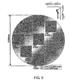
- FIG. 3 shows AFM (Atomic Force Microscope) images of a substrate surface at different positions (9 points) on a silicon substrate.
- Figs. 4(A), (B), and (C) show an atomic model (A), a schematic view (B) thereof, and a correlation diagram (C) of an off angle and an atomic step length (terrace width), for describing steps and terraces, respectively.
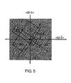
- Fig. 5 shows a plan view for describing a MOS transistor and a crystal direction.
- Figs. 6 (A), (B), and (C) show a sectional view (A) and a three-dimensional overview (B) of the MOS transistor, and a crystal direction view (C) of a substrate respectively.
- a silicon substrate is prepared in which a crystal at a substrate surface has a (100) plane and a plane orientation is inclined by 0.06° as an off angle with respect to the (100) plane in a direction inclined by 36° toward a ⁇ 011> direction with respect to a ⁇ 01-1> direction.
- the off angle is an angle evaluated by XRD (X-Ray Diffraction).
- argon (Ar) atmosphere As an annealing atmosphere, other inactive gases may be used instead of argon (Ar).
- Fig. 3 shows the AFM images at one point of a central part of the semiconductor substrate and at eight points of peripheral parts of the substrate, which are obtained by generally equally dividing a circumference into eight segments. An off direction and an off angle at each point are shown at an upper row and a lower row, respectively.
- the peripheral parts at the eight points encompass a region except an outermost peripheral part of the substrate.
- the AFM images at the nine points are substantially same and the surface of the entire substrate is flattened by a step/terrace structure uniformly extending in the same direction.
- an off direction is 126° and an off angle is 0.056°.
- terrace widths are the same and steps are formed in the same direction.
- the off directions are the same and the off angles are the same throughout the entire surface of the semiconductor substrate.
- the steps and terraces are periodically formed in the same direction throughout the entire surface of the semiconductor substrate.
- a silicon surface is inclined by an off angle ( ⁇ ) from a Just (100) plane.
- ⁇ an off angle
- lattice points on the surface are different as shown in Fig. 4(A) .
- steps S A and S B are formed.
- the steps have a height of 0.13nm which is equal to a mono atomic step on the silicon (100) surface.
- the mono atomic step length L is equal to the terrace width.
- the terrace widths have variation of several atoms. However, the variation is as small as on the order of nm and falls within a range such that the influence on a characteristic is negligible or small. Therefore, the terrace widths are substantially same.
- the directions of the steps are not aligned in a straight line and have unevenness of several atoms at the atomic level. However, the unevenness is also as small as on the order of nm and falls within a range such that the influence on a characteristic is negligible or small. Accordingly, the directions of the steps are regarded to be substantially linear and aligned in one direction. Therefore, the steps are formed in the substantially same direction.
- the off angles are the substantially same angle, similarly as an average angle. In the following description, it will simply be represented that the step directions are the same, the terrace widths are the same, and the off angles are the same.
- Fig. 4(C) shows a relationship between the off angle ( ⁇ ) and a mono atomic step length (L) of the silicon (100) surface.
- a distance between the step S A and the step S B is the mono atomic step length which is the terrace width.
- the off direction (tilt direction) of the substrate with respect to the (100) plane the step and the terrace directions can be controlled and, by the off angle (tilt angle), the terrace width can be controlled.
- the off direction is 126° and the off angle is 0.056°.
- the silicon substrate prepared has the off angle of 0.06°. It is understood that the evaluated off angle of 0.056° falls within the tolerance from the preset off angle of 0.06° and these off angles well correspond with each other.
- the off angle ( ⁇ ) when the off angle ( ⁇ ) is 0.016°, the off direction varies between 25° and 108° depending on a position on the substrate surface and the widths and the directions of the terraces vary also. It is understood that, by controlling the off angle, the substrate according to the present invention can be obtained in which the terraces are aligned in the same direction at any positions on the silicon substrate surface.
- a carrier traveling (transport) direction (source-drain direction) of the MOS transistor is set to a direction in which roughness is extremely small and a carrier mobility is high.
- the carrier traveling direction is set to a direction parallel to the steps so that the steps do not intersect with the carrier traveling direction.
- Non-Patent Document 5 A surface of the semiconductor substrate 1 subjected to the above-mentioned treatment is cleaned by a cleaning method using no alkaline solution (Non-Patent Document 5).
- a SiO 2 film 2 having a thickness of 7nm is formed by radical oxidation in which a substrate surface is directly oxidized by oxygen radicals generated by plasma.
- a SiO 2 film 3 having a thickness of 300nm is formed by CVD.
- An active region where the MOS transistor is to be formed is opened by photolithography.
- a source (S)-drain(D) structure is set in a direction inclined toward a ⁇ 011> direction by 54° with respect to a ⁇ 01-1> direction so that no step exists in the source-drain direction.
- the opening is formed at each of a plurality of (a number of) portions where transistors are to be formed, respectively. In Fig. 6 , one of the opening portions and one of the transistors are shown. Thereafter, an exposed semiconductor surface is cleaned by the cleaning method using no alkaline solution. Then, by radical oxidation, a SiO 2 film 4 having a thickness of 5.6nm is formed as a gate insulating film and polycrystalline polysilicon is formed as a gate electrode 5.
- the thickness of the gate insulating film is mentioned by way of example only.
- isotropic oxidation such as radical oxidation
- an interface flatness is not degraded regardless of a film thickness.
- the MOS transistor can be formed by a normal MOS transistor forming method.
- the MOS transistor is formed by formation of a source diffusion layer 6 and a drain diffusion layer 7, deposition of an interlayer insulating film 8, opening of a contact hole, and formation of a gate extraction electrode 9, a source extraction electrode 10, and a drain extraction electrode 11.
- Fig. 6 shows a sectional view (A) and a three-dimensional overview (B) of the formed MOS transistor, and a crystal orientation view (C) of the substrate respectively.
- the MOS transistor has the silicon substrate surface which is flat at the atomic level and has the source-drain structure formed in the direction inclined toward the ⁇ 011> direction by 54° with respect to the ⁇ 01-1> direction. Therefore, it is possible to realize the MOS transistor in which a silicon/gate-insulating-film interface is flat at the atomic level and which has an extremely low roughness and a high carrier mobility in the carrier traveling direction (source-drain direction).
- the steps and the terraces on the silicon surface are uniform throughout the entire substrate. Therefore, at any portion on the chip taken from any portion on the substrate, the MOS transistor has the same mobility.
- the gate insulating film may be formed by any method as long as the semiconductor substrate is isotropically oxidized or nitrided.
- STI Shallow Trench Isolation
- LOCOS Lical Oxidation of Silicon
- any method may be used as long as the film thickness of the similar level is obtained.
- the semiconductor substrate in which a plurality of terraces formed stepwise by an atomic step are formed in the substantially same direction throughout the substantially entire surface of the semiconductor substrate and in which the semiconductor substrate surface has the substantially same off angle.
- the MOS transistor is formed so that no step exists in the carrier traveling direction (source-drain direction).
- carriers are free from degradation in carrier mobility due to the surface asperity of the substrate and have the same carrier mobility.
Landscapes
- Insulated Gate Type Field-Effect Transistor (AREA)
- Element Separation (AREA)
- Metal-Oxide And Bipolar Metal-Oxide Semiconductor Integrated Circuits (AREA)
Abstract
Description
- This invention relates to a semiconductor substrate, such as a semiconductor wafer, and to a semiconductor device which is formed using the semiconductor substrate.
- Conventionally, an asperity of a substrate surface on which a semiconductor device is formed is represented by using a statistic index, such as an average surface roughness (Ra) (Patent Document 1). Those values, such as 0.02nm, 0.07nm, 0.09nm, and 0.11 nm, which are unrelated to surface atoms are used as the index. This is because there has been no technique of industrially flattening a semiconductor substrate surface at an atomic level and surface flattening has been performed by isotropic oxidation or the like (Non-Patent Document 1).
- In the conventional method, it is impossible, in principle, to eliminate the asperity at the atomic level and, as a result, degradation in carrier mobility is induced in a semiconductor device due to a surface asperity (Non-Patent
Documents 2 and 3). Meanwhile, as regards flattening of a silicon substrate surface, it is reported that the substrate surface inclined by approximately 4 degrees from a silicon crystal plane (100) is flattened at the atomic level by oxidation and etching with a strongly-acid solution with respect to a substrate surface (Non-Patent Document 4). It is also proposed that a (110) plane or a plane inclined from the (110) plane is flattened at the atomic level and provided with a step at the atomic level (Patent Document 2). - In the above-mentioned prior documents, no description is made about the problem addressed by the present invention and the means to solve the problem. The above-mentioned prior documents do not disclose a semiconductor substrate and a semiconductor device, in which steps and terraces are controlled in direction and width throughout a substantially entire area of the substrate surface to suppress degradation in carrier mobility due to the surface asperity.
-
- Patent Document 1:
JP-A-2004-356114 - Patent Document 2:
JP-A-2004-265918 - Non-Patent Document 1: A. Teramoto et al., "Very High Carrier Mobility for High-Performance CMOS on a Si(110) Surface," IEEE Electron Devices, Vol. 54, No. 6, pp.1438-1445, June 2007.
- Non-Patent Document 2: S.Takagi et al., "On the universality of inversion layer mobility in Si MOSFET's: Part I-effects of substrate impurity concentration," IEEE Electron Devices, Vol. 41, No. 12, pp. 2357-2362, Dec. 1994.
- Non-Patent Document 3: T. Ohmi et al., "Revolutional Progress of Silicon Technologies Exhibiting Very High Speed Performance Over a 50-GHz Clock rate," IEEE Electron Devices, Vol. 54, No. 6, pp. 1471-1477, June 2007.
- Non-Patent Document 4: Y. Morita et al., "Atomic scale flattening and hydrogen termination of the Si(001) surface by wet-chemical treatment," J. Vac. Sci. Technol. A, Vac. Surf. Film, Vol. 14, No. 3, pp.854-858, May 1996.
- Non-Patent Document 5: T. Ohmi, "Total room temperature wet cleaning Si substrate surface," J. Electrochem. Soc., Vol.143, No. 9, pp. 2957-2964, Sep. 1996.
- In
Non-Patent Document 4 andPatent Document 2 mentioned above, the substrate surface is flattened at the atomic level. However, it is impossible to control directions of steps and terraces and widths of the terraces at the atomic level.Fig. 1 shows STM (Scanning Tunneling Microscope) images of silicon surfaces. The normal silicon surface shown inFig. 1(A) has a random surface structure and is not flattened at the atomic level. The silicon surface shown inFig. 1(B) according to the technique of Non-PatentDocument 4 is flattened at the atomic level. However, it is understood that the directions of the steps and the terraces and the widths of the terraces at the atomic level are not controlled. Further, in Non-PatentDocument 4, no description is made at all about forming a semiconductor device on the surface and it is impossible to form the semiconductor device. - It is an object of the present invention to provide a semiconductor substrate and a semiconductor device, which are capable of controlling directions and widths of steps and terraces at the atomic level on a semiconductor substrate surface so as to suppress degradation in carrier mobility due to a surface asperity.
- According to the present invention, there is provided a semiconductor substrate characterized in that a substrate surface is provided with a plurality of terraces formed stepwise by an atomic step and formed in the substantially same direction.
- According to the present invention, there is provided the above-mentioned semiconductor substrate characterized in that a crystal at the substrate surface is a silicon crystal and has (100) orientation.
- According to the present invention, there is provided a semiconductor substrate characterized in that a substrate surface has the substantially same off angle throughout an entire surface of the substrate.
- According to the present invention, there is provided a semiconductor substrate characterized in that a substrate surface has the substantially same off angle throughout an entire surface of the substrate and is provided with a plurality of terraces formed stepwise by an atomic step and formed in the substantially same direction.
- According to the present invention, there is provided the above-mentioned semiconductor substrate characterized in that a crystal at the substrate surface is a silicon crystal and has (100) orientation.
- According to the present invention, there is provided the above-mentioned semiconductor substrate characterized in that the terraces have the substantially same direction throughout a substantially entire surface of the substrate.
- According to the present invention, there is provided the above-mentioned semiconductor substrate characterized in that the terraces have the substantially same width throughout a substantially entire surface of the substrate.
- According to the present invention, there is provided a semiconductor device characterized by being formed using the semiconductor substrate.
- According to the present invention, there is provided a semiconductor device characterized by comprising a plurality of semiconductor elements formed on a semiconductor chip provided with a plurality of terraces formed stepwise by an atomic step and formed in the substantially same direction throughout substantially all portions of a semiconductor crystal surface.
- According to the present invention, there is provided the semiconductor device characterized in that the semiconductor elements are formed so that carriers are transported in a direction substantially same as that of the terraces.
- According to the present invention, there is provided the semiconductor device characterized in that the semiconductor elements are MOS transistors and each of the MOS transistors has a source-drain direction substantially same as that of the terraces.
- According to the present invention, there is provided the semiconductor device characterized in that a crystal surface of the semiconductor chip is silicon and has (100) orientation.
- According to the present invention, there is provided the semiconductor substrate characterized in that the terraces have the substantially same direction throughout a substantially entire surface of the substrate.
- According to the present invention, there is provided the semiconductor substrate characterized in that the terraces have the substantially same width throughout a substantially entire surface of the substrate.
- According to the present invention, the directions of the terraces at the atomic level are controlled to be substantially same throughout a substantially entire area of the semiconductor substrate surface. As a result, it is possible to obtain a semiconductor device in which all semiconductor elements of the same size formed at different positions on a chip surface have the same characteristic while it was impossible in the past.
-
-
Fig. 1A shows an AFM image of a normal silicon substrate surface. -
Fig. 1B shows an AFM image of a silicon substrate surface according to the technique of Non-PatentDocument 4. -
Fig. 2A shows AFM images of a semiconductor substrate surface when an off angle is 0.016°. -
Fig. 2B is an atomic schematic view for describing steps and terraces. -
Fig. 2C is a correlation diagram of an off angle and a mono atomic step length (terrace width). -
Fig. 3 shows AFM images of a semiconductor substrate surface in the present invention. -
Fig. 4A is an atomic model view for describing steps and terraces in the present invention. -
Fig. 4B is an atomic schematic view for describing the steps and the terraces in the present invention. -
Fig. 4C is a correlation diagram of an off angle and a mono atomic step length (terrace width) for describing the steps and terraces in the present invention. -
Fig. 5 is a plan view for describing a MOS transistor according to the present invention and a crystal direction. -
Fig. 6A is a sectional view of the MOS transistor according to the present invention. -
Fig. 6B is a three-dimensional overview of the MOS transistor according to the present invention. -
Fig. 6C is a crystal orientation view of a substrate of the MOS transistor according to the present invention. - Hereinbelow, an embodiment of a semiconductor substrate and a semiconductor device according to the present invention will be described in detail with reference to
Figs. 3 through 6 .Fig. 3 shows AFM (Atomic Force Microscope) images of a substrate surface at different positions (9 points) on a silicon substrate.Figs. 4(A), (B), and (C) show an atomic model (A), a schematic view (B) thereof, and a correlation diagram (C) of an off angle and an atomic step length (terrace width), for describing steps and terraces, respectively.Fig. 5 shows a plan view for describing a MOS transistor and a crystal direction.Figs. 6 (A), (B), and (C) show a sectional view (A) and a three-dimensional overview (B) of the MOS transistor, and a crystal direction view (C) of a substrate respectively. - A silicon substrate is prepared in which a crystal at a substrate surface has a (100) plane and a plane orientation is inclined by 0.06° as an off angle with respect to the (100) plane in a direction inclined by 36° toward a <011> direction with respect to a <01-1> direction. The off angle is an angle evaluated by XRD (X-Ray Diffraction). The substrate surface is treated with a solution of HF/H2O = 0.05% to peel an oxide film on the surface and subjected to heat treatment (annealing) in an argon (Ar) atmosphere at 1200°C for 30 minutes. As an annealing atmosphere, other inactive gases may be used instead of argon (Ar).
- The AFM images of the silicon substrate surface are shown in
Fig. 3. Fig. 3 shows the AFM images at one point of a central part of the semiconductor substrate and at eight points of peripheral parts of the substrate, which are obtained by generally equally dividing a circumference into eight segments. An off direction and an off angle at each point are shown at an upper row and a lower row, respectively. The peripheral parts at the eight points encompass a region except an outermost peripheral part of the substrate. By the nine points in total including the one point at the central part, it is possible to evaluate an entire surface of the substrate. A substantially entire surface of the semiconductor substrate may be a narrower region where a number of semiconductor elements are actually formed. It is understood that the AFM images at the nine points are substantially same and the surface of the entire substrate is flattened by a step/terrace structure uniformly extending in the same direction. In all of evaluation results at the nine points, an off direction is 126° and an off angle is 0.056°. Throughout the entire surface of the semiconductor substrate, terrace widths are the same and steps are formed in the same direction. Also, the off directions are the same and the off angles are the same throughout the entire surface of the semiconductor substrate. As mentioned above, the steps and terraces are periodically formed in the same direction throughout the entire surface of the semiconductor substrate. - Referring to
Fig. 4 in addition, the step/terrace structure will be described. Herein, a silicon surface is inclined by an off angle (θ) from a Just (100) plane. At the atomic level, in a case of inclination by the off angle (θ), lattice points on the surface are different as shown inFig. 4(A) . At positions where the lattice points on the surface are changed, steps SA and SB are formed. The steps have a height of 0.13nm which is equal to a mono atomic step on the silicon (100) surface. As shown inFig. 4(B) , in a case of an off angle (0.06°), an average mono atomic step length is L = 0.13/sin(0.06°) = 124nm. The mono atomic step length L is equal to the terrace width. - At the atomic level, the terrace widths have variation of several atoms. However, the variation is as small as on the order of nm and falls within a range such that the influence on a characteristic is negligible or small. Therefore, the terrace widths are substantially same. Likewise the directions of the steps are not aligned in a straight line and have unevenness of several atoms at the atomic level. However, the unevenness is also as small as on the order of nm and falls within a range such that the influence on a characteristic is negligible or small. Accordingly, the directions of the steps are regarded to be substantially linear and aligned in one direction. Therefore, the steps are formed in the substantially same direction. Further, the off angles are the substantially same angle, similarly as an average angle. In the following description, it will simply be represented that the step directions are the same, the terrace widths are the same, and the off angles are the same.
-
Fig. 4(C) shows a relationship between the off angle (θ) and a mono atomic step length (L) of the silicon (100) surface. A distance between the step SA and the step SB is the mono atomic step length which is the terrace width. The step has the height of 0.13nm which is the mono atomic step on the silicon (100) surface and an average value of terrace widths having the off angle (0.06°) is 124nm (= 0.13/sin(0.06°)). It is understood that average values of terrace widths having off angles of (0.03°), (0.5°), and (4.0°) are approximately 250nm, 15nm, and 2nm, respectively. Thus, by the off direction (tilt direction) of the substrate with respect to the (100) plane, the step and the terrace directions can be controlled and, by the off angle (tilt angle), the terrace width can be controlled. - In the AFM images in
Fig. 3 , evaluation results are obtained which show that the off direction is 126° and the off angle is 0.056°. The silicon substrate prepared has the off angle of 0.06°. It is understood that the evaluated off angle of 0.056° falls within the tolerance from the preset off angle of 0.06° and these off angles well correspond with each other. The terrace widths are uniform and the same and the directions of the steps are linear. As mentioned above, by the off angle (θ), the terrace width = 0.13/sin θ (θ: off angle) can be controlled. Thus, by setting the off direction and the off angle, it is possible to obtain a step/terrace structure which is linear and periodical in a specific direction. - Now referring to
Fig. 2 , when the off angle (θ) is 0.016°, the off direction varies between 25° and 108° depending on a position on the substrate surface and the widths and the directions of the terraces vary also. It is understood that, by controlling the off angle, the substrate according to the present invention can be obtained in which the terraces are aligned in the same direction at any positions on the silicon substrate surface. - Referring to
Figs. 5 and6 , description will be made about a method of forming a MOS transistor using a semiconductor substrate 1 which is treated as illustrated inFig. 3 . As shown inFig. 5 , a carrier traveling (transport) direction (source-drain direction) of the MOS transistor is set to a direction in which roughness is extremely small and a carrier mobility is high. Specifically, the carrier traveling direction is set to a direction parallel to the steps so that the steps do not intersect with the carrier traveling direction. With this structure, it is possible to realize a MOS transistor having an extremely small roughness and a high carrier mobility in the carrier traveling direction. - A surface of the semiconductor substrate 1 subjected to the above-mentioned treatment is cleaned by a cleaning method using no alkaline solution (Non-Patent Document 5). A SiO2 film 2 having a thickness of 7nm is formed by radical oxidation in which a substrate surface is directly oxidized by oxygen radicals generated by plasma. Thereafter, a SiO2 film 3 having a thickness of 300nm is formed by CVD. An active region where the MOS transistor is to be formed is opened by photolithography. At this time, as shown in
Fig. 5 , a source (S)-drain(D) structure is set in a direction inclined toward a <011> direction by 54° with respect to a <01-1> direction so that no step exists in the source-drain direction. - Using photoresist as a mask material, the SiO2 film 2 and the SiO2 film 3 at an opening portion are removed by a solution of HCl/HF = 19/1. The photoresist is removed by a solution of H2SO4/H2O2 = 4:1. The opening is formed at each of a plurality of (a number of) portions where transistors are to be formed, respectively. In
Fig. 6 , one of the opening portions and one of the transistors are shown. Thereafter, an exposed semiconductor surface is cleaned by the cleaning method using no alkaline solution. Then, by radical oxidation, a SiO2 film 4 having a thickness of 5.6nm is formed as a gate insulating film and polycrystalline polysilicon is formed as agate electrode 5. Herein, the thickness of the gate insulating film is mentioned by way of example only. In a case of isotropic oxidation, such as radical oxidation, an interface flatness is not degraded regardless of a film thickness. Thereafter, the MOS transistor can be formed by a normal MOS transistor forming method. For example, the MOS transistor is formed by formation of asource diffusion layer 6 and adrain diffusion layer 7, deposition of an interlayer insulating film 8, opening of a contact hole, and formation of agate extraction electrode 9, asource extraction electrode 10, and adrain extraction electrode 11. -
Fig. 6 shows a sectional view (A) and a three-dimensional overview (B) of the formed MOS transistor, and a crystal orientation view (C) of the substrate respectively. The MOS transistor has the silicon substrate surface which is flat at the atomic level and has the source-drain structure formed in the direction inclined toward the <011> direction by 54° with respect to the <01-1> direction. Therefore, it is possible to realize the MOS transistor in which a silicon/gate-insulating-film interface is flat at the atomic level and which has an extremely low roughness and a high carrier mobility in the carrier traveling direction (source-drain direction). The steps and the terraces on the silicon surface are uniform throughout the entire substrate. Therefore, at any portion on the chip taken from any portion on the substrate, the MOS transistor has the same mobility. - There is no special limitation on the method of forming the MOS transistor. The gate insulating film may be formed by any method as long as the semiconductor substrate is isotropically oxidized or nitrided. As a technique of device isolation between a number of transistors thus formed, STI (Shallow Trench Isolation), LOCOS (Local Oxidation of Silicon), or the like may be used. As a method of cleaning a surface of the active region and a method of forming an oxide film or a nitride film, any method may be used as long as the film thickness of the similar level is obtained.
- According to the present invention, it is possible to obtain the semiconductor substrate in which a plurality of terraces formed stepwise by an atomic step are formed in the substantially same direction throughout the substantially entire surface of the semiconductor substrate and in which the semiconductor substrate surface has the substantially same off angle. Using the semiconductor substrate, the MOS transistor is formed so that no step exists in the carrier traveling direction (source-drain direction). In the MOS transistor, carriers are free from degradation in carrier mobility due to the surface asperity of the substrate and have the same carrier mobility. As a result, it is possible to obtain the semiconductor device in which all semiconductor elements of the same size formed at different positions on a surface of a semiconductor chip have the same characteristic.
- In the foregoing, the present invention has been described in detail based on the embodiment. However, it will readily be understood that the present invention is not limited to the above-mentioned embodiment and may be modified in various manners within the scope of the present invention.
- This application claims priority based on Japanese Patent Application No.
2007-261096 filed on October 4, 2007
Claims (14)
- A semiconductor substrate characterized in that a substrate surface is provided with a plurality of terraces formed stepwise by an atomic step and formed in the substantially same direction.
- The semiconductor substrate as claimed in claim 1, characterized in that a crystal at the substrate surface is a silicon crystal and has (100) orientation.
- A semiconductor substrate characterized in that a substrate surface has the substantially same off angle throughout an entire surface of the substrate.
- A semiconductor substrate characterized in that a substrate surface has the substantially same off angle throughout an entire surface of the substrate and is provided with a plurality of terraces formed stepwise by an atomic step and formed in the substantially same direction.
- The semiconductor substrate as claimed in claim 4, characterized in that a crystal at the substrate surface is a silicon crystal and has (100) orientation.
- The semiconductor substrate as claimed in any one of claims 1, 2, 4, and 5, characterized in that the terraces have the substantially same direction throughout a substantially entire surface of the substrate.
- The semiconductor substrate as claimed in any one of claims 1, 2, 4, 5, and 6, characterized in that the terraces have the substantially same width throughout a substantially entire surface of the substrate.
- A semiconductor device characterized by being formed using the semiconductor substrate claimed in any one of claims 1 through 7.
- A semiconductor device characterized by comprising a plurality of semiconductor elements formed on a semiconductor chip provided with a plurality of terraces formed stepwise by an atomic step and formed in the substantially same direction throughout substantially all portions of a semiconductor crystal surface.
- The semiconductor device as claimed in claim 9, characterized in that the semiconductor elements are formed so that carriers are transported in a direction substantially same as that of the terraces.
- The semiconductor device as claimed in claim 10, characterized in that the semiconductor elements are MOS transistors and each of the MOS transistors has a source-drain direction substantially same as that of the terraces.
- The semiconductor device as claimed in any one of claims 9 through 11, characterized in that a crystal surface of the semiconductor chip is silicon and has (100) orientation.
- The semiconductor device as claimed in any one of claims 9 through 12, characterized in that the terraces have the substantially same direction throughout a substantially entire surface of the semiconductor chip.
- The semiconductor device as claimed in any one of claims 9 through 13, characterized in that the terraces have the substantially same width throughout a substantially entire surface of the semiconductor chip.
Applications Claiming Priority (2)
| Application Number | Priority Date | Filing Date | Title |
|---|---|---|---|
| JP2007261096A JP2009094156A (en) | 2007-10-04 | 2007-10-04 | Semiconductor substrate and semiconductor device |
| PCT/JP2008/068183 WO2009044917A1 (en) | 2007-10-04 | 2008-10-06 | Semiconductor substrate and semiconductor device |
Publications (2)
| Publication Number | Publication Date |
|---|---|
| EP2197023A1 true EP2197023A1 (en) | 2010-06-16 |
| EP2197023A4 EP2197023A4 (en) | 2013-05-22 |
Family
ID=40526329
Family Applications (1)
| Application Number | Title | Priority Date | Filing Date |
|---|---|---|---|
| EP08835197.8A Ceased EP2197023A4 (en) | 2007-10-04 | 2008-10-06 | SEMICONDUCTOR SUBSTRATE AND SEMICONDUCTOR DEVICE |
Country Status (6)
| Country | Link |
|---|---|
| US (1) | US8492879B2 (en) |
| EP (1) | EP2197023A4 (en) |
| JP (1) | JP2009094156A (en) |
| KR (1) | KR101536020B1 (en) |
| CN (1) | CN101816060B (en) |
| WO (1) | WO2009044917A1 (en) |
Families Citing this family (4)
| Publication number | Priority date | Publication date | Assignee | Title |
|---|---|---|---|---|
| US8445386B2 (en) * | 2010-05-27 | 2013-05-21 | Cree, Inc. | Smoothing method for semiconductor material and wafers produced by same |
| WO2012172774A1 (en) * | 2011-06-13 | 2012-12-20 | パナソニック株式会社 | Method for manufacturing semiconductor device |
| JP2016006870A (en) * | 2014-05-30 | 2016-01-14 | 住友電気工業株式会社 | Semiconductor device |
| KR102662765B1 (en) | 2018-08-02 | 2024-05-02 | 삼성전자주식회사 | Substrate, integrated circuit device including substrate, and method of manufacturing integrated circuit device |
Family Cites Families (8)
| Publication number | Priority date | Publication date | Assignee | Title |
|---|---|---|---|---|
| DE19611043B4 (en) * | 1995-03-20 | 2006-02-16 | Toshiba Ceramics Co., Ltd. | A method of producing a silicon wafer, a method of forming a silicon wafer, and a method of manufacturing a semiconductor device |
| DE69617100T2 (en) * | 1995-05-31 | 2002-07-18 | Matsushita Electric Ind Co Ltd | MOSFET channel zone and manufacturing process |
| US6559518B1 (en) * | 1998-10-01 | 2003-05-06 | Matsushita Electric Industrial Co., Ltd. | MOS heterostructure, semiconductor device with the structure, and method for fabricating the semiconductor device |
| JP4651207B2 (en) * | 2001-02-26 | 2011-03-16 | 京セラ株式会社 | Semiconductor substrate and manufacturing method thereof |
| DE10237247B4 (en) * | 2002-08-14 | 2004-09-09 | Siltronic Ag | Method of manufacturing a silicon wafer |
| JP4190906B2 (en) * | 2003-02-07 | 2008-12-03 | 信越半導体株式会社 | Silicon semiconductor substrate and manufacturing method thereof |
| JP2004356114A (en) * | 2003-05-26 | 2004-12-16 | Tadahiro Omi | P-channel power MIS field-effect transistor and switching circuit |
| JP2007261096A (en) | 2006-03-28 | 2007-10-11 | Ricoh Co Ltd | Ink jet printer, printing method, printing program, and recording medium |
-
2007
- 2007-10-04 JP JP2007261096A patent/JP2009094156A/en not_active Ceased
-
2008
- 2008-10-06 CN CN2008801102861A patent/CN101816060B/en active Active
- 2008-10-06 WO PCT/JP2008/068183 patent/WO2009044917A1/en not_active Ceased
- 2008-10-06 US US12/681,576 patent/US8492879B2/en active Active
- 2008-10-06 KR KR1020107007609A patent/KR101536020B1/en active Active
- 2008-10-06 EP EP08835197.8A patent/EP2197023A4/en not_active Ceased
Also Published As
| Publication number | Publication date |
|---|---|
| CN101816060B (en) | 2012-01-11 |
| WO2009044917A1 (en) | 2009-04-09 |
| JP2009094156A (en) | 2009-04-30 |
| US8492879B2 (en) | 2013-07-23 |
| KR101536020B1 (en) | 2015-07-10 |
| US20100213516A1 (en) | 2010-08-26 |
| KR20100067107A (en) | 2010-06-18 |
| CN101816060A (en) | 2010-08-25 |
| EP2197023A4 (en) | 2013-05-22 |
Similar Documents
| Publication | Publication Date | Title |
|---|---|---|
| US10833156B2 (en) | Self-forming spacers using oxidation | |
| US12408367B2 (en) | Semiconductor device | |
| US9496144B2 (en) | Method of fabricating a charge-trapping gate stack using a CMOS process flow | |
| CN1253943C (en) | Transistor with multiple gates and strained channel layer and method of manufacturing the same | |
| US6998305B2 (en) | Enhanced selectivity for epitaxial deposition | |
| US7411274B2 (en) | Silicon semiconductor substrate and its manufacturing method | |
| US9876088B1 (en) | III-V semiconductor layers, III-V semiconductor devices and methods of manufacturing thereof | |
| CN107026127A (en) | The extension facet high consistency of FDSOI technologies is improved | |
| WO2012100396A1 (en) | Semiconductor device and method for manufacturing same | |
| US9876117B2 (en) | Structure and formation method of semiconductor device structure | |
| US20210305375A1 (en) | Semiconductor device including fin and method for manufacturing the same | |
| US8492879B2 (en) | Semiconductor substrate and semiconductor device | |
| JP5388312B2 (en) | GERMANIUM STRUCTURE AND METHOD FOR FORMING THE SAME, METHOD FOR FORMING TRANSISTOR STRUCTURE | |
| EP2533270A1 (en) | Silicon wafer and semiconductor device | |
| CN105826232A (en) | Formation method of semiconductor structure | |
| JP4376505B2 (en) | Manufacturing method of semiconductor device | |
| US10600890B2 (en) | Contact to metal gate isolation structure | |
| JP2013254982A (en) | Semiconductor substrate and semiconductor device | |
| CN106952807A (en) | Semiconductor structure and forming method thereof | |
| CN105336569A (en) | Semiconductor device manufacturing method | |
| US20080188089A1 (en) | Method for reducing top notching effects in pre-doped gate structures |
Legal Events
| Date | Code | Title | Description |
|---|---|---|---|
| PUAI | Public reference made under article 153(3) epc to a published international application that has entered the european phase |
Free format text: ORIGINAL CODE: 0009012 |
|
| 17P | Request for examination filed |
Effective date: 20100331 |
|
| AK | Designated contracting states |
Kind code of ref document: A1 Designated state(s): AT BE BG CH CY CZ DE DK EE ES FI FR GB GR HR HU IE IS IT LI LT LU LV MC MT NL NO PL PT RO SE SI SK TR |
|
| AX | Request for extension of the european patent |
Extension state: AL BA MK RS |
|
| RIN1 | Information on inventor provided before grant (corrected) |
Inventor name: HAYAMI, YOSHINORI Inventor name: TERAMOTO, AKINOBU Inventor name: OHMI, TADAHIRO Inventor name: KURODA, RIHITO Inventor name: SUWA, TOMOYUKI Inventor name: KUDO, HIDEO |
|
| DAX | Request for extension of the european patent (deleted) | ||
| A4 | Supplementary search report drawn up and despatched |
Effective date: 20130423 |
|
| RIC1 | Information provided on ipc code assigned before grant |
Ipc: H01L 29/04 20060101ALI20130417BHEP Ipc: H01L 21/02 20060101AFI20130417BHEP Ipc: H01L 29/78 20060101ALI20130417BHEP Ipc: H01L 21/324 20060101ALN20130417BHEP |
|
| 17Q | First examination report despatched |
Effective date: 20140102 |
|
| RAP1 | Party data changed (applicant data changed or rights of an application transferred) |
Owner name: NATIONAL UNIVERSITY CORPORATION TOHOKU UNIVERSITY Owner name: SHIN-ETSU HANDOTAI CO., LTD. |
|
| REG | Reference to a national code |
Ref country code: DE Ref legal event code: R003 |
|
| STAA | Information on the status of an ep patent application or granted ep patent |
Free format text: STATUS: THE APPLICATION HAS BEEN REFUSED |
|
| 18R | Application refused |
Effective date: 20181004 |