EP2196564A1 - Isotope diamond laminate - Google Patents
Isotope diamond laminate Download PDFInfo
- Publication number
- EP2196564A1 EP2196564A1 EP08834751A EP08834751A EP2196564A1 EP 2196564 A1 EP2196564 A1 EP 2196564A1 EP 08834751 A EP08834751 A EP 08834751A EP 08834751 A EP08834751 A EP 08834751A EP 2196564 A1 EP2196564 A1 EP 2196564A1
- Authority
- EP
- European Patent Office
- Prior art keywords
- isotope
- diamond
- film
- stacked body
- substrate
- Prior art date
- Legal status (The legal status is an assumption and is not a legal conclusion. Google has not performed a legal analysis and makes no representation as to the accuracy of the status listed.)
- Granted
Links
Images


Classifications
-
- C—CHEMISTRY; METALLURGY
- C23—COATING METALLIC MATERIAL; COATING MATERIAL WITH METALLIC MATERIAL; CHEMICAL SURFACE TREATMENT; DIFFUSION TREATMENT OF METALLIC MATERIAL; COATING BY VACUUM EVAPORATION, BY SPUTTERING, BY ION IMPLANTATION OR BY CHEMICAL VAPOUR DEPOSITION, IN GENERAL; INHIBITING CORROSION OF METALLIC MATERIAL OR INCRUSTATION IN GENERAL
- C23C—COATING METALLIC MATERIAL; COATING MATERIAL WITH METALLIC MATERIAL; SURFACE TREATMENT OF METALLIC MATERIAL BY DIFFUSION INTO THE SURFACE, BY CHEMICAL CONVERSION OR SUBSTITUTION; COATING BY VACUUM EVAPORATION, BY SPUTTERING, BY ION IMPLANTATION OR BY CHEMICAL VAPOUR DEPOSITION, IN GENERAL
- C23C16/00—Chemical coating by decomposition of gaseous compounds, without leaving reaction products of surface material in the coating, i.e. chemical vapour deposition [CVD] processes
- C23C16/22—Chemical coating by decomposition of gaseous compounds, without leaving reaction products of surface material in the coating, i.e. chemical vapour deposition [CVD] processes characterised by the deposition of inorganic material, other than metallic material
- C23C16/26—Deposition of carbon only
- C23C16/27—Diamond only
-
- C—CHEMISTRY; METALLURGY
- C23—COATING METALLIC MATERIAL; COATING MATERIAL WITH METALLIC MATERIAL; CHEMICAL SURFACE TREATMENT; DIFFUSION TREATMENT OF METALLIC MATERIAL; COATING BY VACUUM EVAPORATION, BY SPUTTERING, BY ION IMPLANTATION OR BY CHEMICAL VAPOUR DEPOSITION, IN GENERAL; INHIBITING CORROSION OF METALLIC MATERIAL OR INCRUSTATION IN GENERAL
- C23C—COATING METALLIC MATERIAL; COATING MATERIAL WITH METALLIC MATERIAL; SURFACE TREATMENT OF METALLIC MATERIAL BY DIFFUSION INTO THE SURFACE, BY CHEMICAL CONVERSION OR SUBSTITUTION; COATING BY VACUUM EVAPORATION, BY SPUTTERING, BY ION IMPLANTATION OR BY CHEMICAL VAPOUR DEPOSITION, IN GENERAL
- C23C16/00—Chemical coating by decomposition of gaseous compounds, without leaving reaction products of surface material in the coating, i.e. chemical vapour deposition [CVD] processes
- C23C16/44—Chemical coating by decomposition of gaseous compounds, without leaving reaction products of surface material in the coating, i.e. chemical vapour deposition [CVD] processes characterised by the method of coating
- C23C16/455—Chemical coating by decomposition of gaseous compounds, without leaving reaction products of surface material in the coating, i.e. chemical vapour deposition [CVD] processes characterised by the method of coating characterised by the method used for introducing gases into reaction chamber or for modifying gas flows in reaction chamber
- C23C16/45523—Pulsed gas flow or change of composition over time
-
- C—CHEMISTRY; METALLURGY
- C30—CRYSTAL GROWTH
- C30B—SINGLE-CRYSTAL GROWTH; UNIDIRECTIONAL SOLIDIFICATION OF EUTECTIC MATERIAL OR UNIDIRECTIONAL DEMIXING OF EUTECTOID MATERIAL; REFINING BY ZONE-MELTING OF MATERIAL; PRODUCTION OF A HOMOGENEOUS POLYCRYSTALLINE MATERIAL WITH DEFINED STRUCTURE; SINGLE CRYSTALS OR HOMOGENEOUS POLYCRYSTALLINE MATERIAL WITH DEFINED STRUCTURE; AFTER-TREATMENT OF SINGLE CRYSTALS OR A HOMOGENEOUS POLYCRYSTALLINE MATERIAL WITH DEFINED STRUCTURE; APPARATUS THEREFOR
- C30B25/00—Single-crystal growth by chemical reaction of reactive gases, e.g. chemical vapour-deposition growth
- C30B25/02—Epitaxial-layer growth
- C30B25/10—Heating of the reaction chamber or the substrate
- C30B25/105—Heating of the reaction chamber or the substrate by irradiation or electric discharge
-
- C—CHEMISTRY; METALLURGY
- C30—CRYSTAL GROWTH
- C30B—SINGLE-CRYSTAL GROWTH; UNIDIRECTIONAL SOLIDIFICATION OF EUTECTIC MATERIAL OR UNIDIRECTIONAL DEMIXING OF EUTECTOID MATERIAL; REFINING BY ZONE-MELTING OF MATERIAL; PRODUCTION OF A HOMOGENEOUS POLYCRYSTALLINE MATERIAL WITH DEFINED STRUCTURE; SINGLE CRYSTALS OR HOMOGENEOUS POLYCRYSTALLINE MATERIAL WITH DEFINED STRUCTURE; AFTER-TREATMENT OF SINGLE CRYSTALS OR A HOMOGENEOUS POLYCRYSTALLINE MATERIAL WITH DEFINED STRUCTURE; APPARATUS THEREFOR
- C30B29/00—Single crystals or homogeneous polycrystalline material with defined structure characterised by the material or by their shape
- C30B29/02—Elements
- C30B29/04—Diamond
-
- H—ELECTRICITY
- H10—SEMICONDUCTOR DEVICES; ELECTRIC SOLID-STATE DEVICES NOT OTHERWISE PROVIDED FOR
- H10P—GENERIC PROCESSES OR APPARATUS FOR THE MANUFACTURE OR TREATMENT OF DEVICES COVERED BY CLASS H10
- H10P14/00—Formation of materials, e.g. in the shape of layers or pillars
- H10P14/20—Formation of materials, e.g. in the shape of layers or pillars of semiconductor materials
-
- H—ELECTRICITY
- H10—SEMICONDUCTOR DEVICES; ELECTRIC SOLID-STATE DEVICES NOT OTHERWISE PROVIDED FOR
- H10P—GENERIC PROCESSES OR APPARATUS FOR THE MANUFACTURE OR TREATMENT OF DEVICES COVERED BY CLASS H10
- H10P14/00—Formation of materials, e.g. in the shape of layers or pillars
- H10P14/20—Formation of materials, e.g. in the shape of layers or pillars of semiconductor materials
- H10P14/24—Formation of materials, e.g. in the shape of layers or pillars of semiconductor materials using chemical vapour deposition [CVD]
-
- H—ELECTRICITY
- H10—SEMICONDUCTOR DEVICES; ELECTRIC SOLID-STATE DEVICES NOT OTHERWISE PROVIDED FOR
- H10P—GENERIC PROCESSES OR APPARATUS FOR THE MANUFACTURE OR TREATMENT OF DEVICES COVERED BY CLASS H10
- H10P14/00—Formation of materials, e.g. in the shape of layers or pillars
- H10P14/20—Formation of materials, e.g. in the shape of layers or pillars of semiconductor materials
- H10P14/29—Formation of materials, e.g. in the shape of layers or pillars of semiconductor materials characterised by the substrates
- H10P14/2901—Materials
- H10P14/2902—Materials being Group IVA materials
- H10P14/2903—Carbon, e.g. diamond-like carbon
-
- H—ELECTRICITY
- H10—SEMICONDUCTOR DEVICES; ELECTRIC SOLID-STATE DEVICES NOT OTHERWISE PROVIDED FOR
- H10P—GENERIC PROCESSES OR APPARATUS FOR THE MANUFACTURE OR TREATMENT OF DEVICES COVERED BY CLASS H10
- H10P14/00—Formation of materials, e.g. in the shape of layers or pillars
- H10P14/20—Formation of materials, e.g. in the shape of layers or pillars of semiconductor materials
- H10P14/32—Formation of materials, e.g. in the shape of layers or pillars of semiconductor materials characterised by intermediate layers between substrates and deposited layers
- H10P14/3202—Materials thereof
- H10P14/3204—Materials thereof being Group IVA semiconducting materials
- H10P14/3206—Carbon, e.g. diamond-like carbon
-
- H—ELECTRICITY
- H10—SEMICONDUCTOR DEVICES; ELECTRIC SOLID-STATE DEVICES NOT OTHERWISE PROVIDED FOR
- H10P—GENERIC PROCESSES OR APPARATUS FOR THE MANUFACTURE OR TREATMENT OF DEVICES COVERED BY CLASS H10
- H10P14/00—Formation of materials, e.g. in the shape of layers or pillars
- H10P14/20—Formation of materials, e.g. in the shape of layers or pillars of semiconductor materials
- H10P14/32—Formation of materials, e.g. in the shape of layers or pillars of semiconductor materials characterised by intermediate layers between substrates and deposited layers
- H10P14/3242—Structure
- H10P14/3244—Layer structure
- H10P14/3251—Layer structure consisting of three or more layers
- H10P14/3252—Alternating layers, e.g. superlattice
-
- H—ELECTRICITY
- H10—SEMICONDUCTOR DEVICES; ELECTRIC SOLID-STATE DEVICES NOT OTHERWISE PROVIDED FOR
- H10P—GENERIC PROCESSES OR APPARATUS FOR THE MANUFACTURE OR TREATMENT OF DEVICES COVERED BY CLASS H10
- H10P14/00—Formation of materials, e.g. in the shape of layers or pillars
- H10P14/20—Formation of materials, e.g. in the shape of layers or pillars of semiconductor materials
- H10P14/34—Deposited materials, e.g. layers
- H10P14/3402—Deposited materials, e.g. layers characterised by the chemical composition
- H10P14/3404—Deposited materials, e.g. layers characterised by the chemical composition being Group IVA materials
- H10P14/3406—Carbon, e.g. diamond-like carbon
-
- Y—GENERAL TAGGING OF NEW TECHNOLOGICAL DEVELOPMENTS; GENERAL TAGGING OF CROSS-SECTIONAL TECHNOLOGIES SPANNING OVER SEVERAL SECTIONS OF THE IPC; TECHNICAL SUBJECTS COVERED BY FORMER USPC CROSS-REFERENCE ART COLLECTIONS [XRACs] AND DIGESTS
- Y10—TECHNICAL SUBJECTS COVERED BY FORMER USPC
- Y10T—TECHNICAL SUBJECTS COVERED BY FORMER US CLASSIFICATION
- Y10T428/00—Stock material or miscellaneous articles
- Y10T428/24—Structurally defined web or sheet [e.g., overall dimension, etc.]
- Y10T428/24942—Structurally defined web or sheet [e.g., overall dimension, etc.] including components having same physical characteristic in differing degree
- Y10T428/2495—Thickness [relative or absolute]
-
- Y—GENERAL TAGGING OF NEW TECHNOLOGICAL DEVELOPMENTS; GENERAL TAGGING OF CROSS-SECTIONAL TECHNOLOGIES SPANNING OVER SEVERAL SECTIONS OF THE IPC; TECHNICAL SUBJECTS COVERED BY FORMER USPC CROSS-REFERENCE ART COLLECTIONS [XRACs] AND DIGESTS
- Y10—TECHNICAL SUBJECTS COVERED BY FORMER USPC
- Y10T—TECHNICAL SUBJECTS COVERED BY FORMER US CLASSIFICATION
- Y10T428/00—Stock material or miscellaneous articles
- Y10T428/24—Structurally defined web or sheet [e.g., overall dimension, etc.]
- Y10T428/24942—Structurally defined web or sheet [e.g., overall dimension, etc.] including components having same physical characteristic in differing degree
- Y10T428/2495—Thickness [relative or absolute]
- Y10T428/24967—Absolute thicknesses specified
- Y10T428/24975—No layer or component greater than 5 mils thick
-
- Y—GENERAL TAGGING OF NEW TECHNOLOGICAL DEVELOPMENTS; GENERAL TAGGING OF CROSS-SECTIONAL TECHNOLOGIES SPANNING OVER SEVERAL SECTIONS OF THE IPC; TECHNICAL SUBJECTS COVERED BY FORMER USPC CROSS-REFERENCE ART COLLECTIONS [XRACs] AND DIGESTS
- Y10—TECHNICAL SUBJECTS COVERED BY FORMER USPC
- Y10T—TECHNICAL SUBJECTS COVERED BY FORMER US CLASSIFICATION
- Y10T428/00—Stock material or miscellaneous articles
- Y10T428/30—Self-sustaining carbon mass or layer with impregnant or other layer
Definitions
- the present invention relates to a stacked body of isotope diamond and a method of producing the same.
- One of the remarkable crystal designing technology is related to a semiconductor super-lattices constituted of different semiconductor materials alternately stacked in planer ( one dimensional ), linier (two dimensional), or blocked (three dimensional) arrangement.
- An important concept of this technology is in that electric structure of a crystal can be modulated by stacking two layers of semiconductor materials having different band-gap, or by forming a periodic structure in which the two-layered structure as a unit structure is repeated.
- the super-lattice is a crystal formed by artificially stacking different semiconductor materials each having a layer thickness of mono-atomic thickness to several 10s nm (typically, about 50 nm) to provide a long-range periodical structure. Numerous physical phenomena which are not shown by a bulk single crystal are observed in the super-lattice, providing various fundamental problems not only in the field of physics, but also in the field of application.
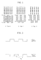
- FIGS. 1(a) to (c) shows a super-lattice of type I, type I', and type II respectively.
- Ec and Ev respectively denote conduction band and valence band.
- conduction band and valence band of each of two semiconductors 1 and 2 overlap each other, and the band-gap changes discontinuously.
- type I super lattice As a representative stacked (layered) structure of type I super lattice, there exists a structure in which GaAs is used in semiconductor 1 and Al x Ga 1-x As is used in semiconductor 2. As a representative stacked structure of type I' super lattice, there exists a structure in which In 1-x Ga x As and GaSb 1-y As y are used in semiconductor 1 and semiconductor 2 respectively. On the other hand, in a type II super lattice, valence band of a semiconductor overlaps the conduction band of the other semiconductor. As a representative stacked structure of this type super lattice, there exists a structure in which InAs is used as the semiconductor 1 and GaSb is used as the semiconductor 2.
- electronic state of a super lattice may be characterized by another parameters.
- electronic state of type I super-lattice may be approximately expressed by a square-well potential as shown in FIG. 2 .
- the electronic state depends on four parameters shown by with Lw of the well and with L B of the barriers.
- L W and L B are each controlled to be a similar level as de Bloglie wavelength of an electron (for example, in GaAs-Al x Ga 1-x As, L W may be controlled to be 30 nm or less, and L B may be controlled to be 10 nm or less), periodic potential longer than usual lattice spacing is introduced into a crystal, and a mini-band is formed. As a result, the role of the quantum effect is shown remarkably.
- electrons can transmit (propagate) in a material with high mobility. Such electrons are actually used in some devices.
- a representative device is a High Electron Mobility Transistor (HEMT).
- HEMT High Electron Mobility Transistor
- secondary electron gas having extremely high mobility is formed in the layers of semiconductor 1 by a modulation doping super lattice structure in which doping (for example introduction of n-type dopant) is performed only in the layers of semiconductor 2 of a type I super lattice.
- an active layer for transmitting electron current includes impurities for ensuring a conduction, but the impurities act as the the dominant scattering factor that suppresses the mobility of electrons.
- the impurities act as the the dominant scattering factor that suppresses the mobility of electrons.
- the electrons hardly suffer scattering by the impurities, and mobility is largely improved, enabling actual use.
- HEMT HEMT utilizing a wide band-gap semiconductor is paid attention to as a device by which high-temperature, high-current, and high withstand voltage operation, and GaN-AlGaN based HEMT is proposed as an alternative to the conventional GaAs-AlGaAs based HEMT.
- L B is controlled to be sufficiently larger than L W , it is possible to form a single-well state that confine carriers in a desired semiconductor layer. This is due to a carrier trapping effect utilizing an energy barrier caused by the difference in band-gaps, and is one of the main characteristics of a super-lattice.
- a quantum-well laser is a representative example. For example, in the quantum-well laser, shortening of wavelength of laser oscillation, improvement of thermal variation of threshold current density, and enhancement of luminous efficiency are realized along with reduction of L W (for example, GaAs layer is reduced from 20 nm in type I GaAs-Al x Ga 1-x As).
- thin film crystallization technology for example, by Molecular Beam Epitaxy (MBE) or Organometallic Vapor Phase Epitaxy (OMVPE) using organic metals is used in realization of a super lattice structure.
- MBE Molecular Beam Epitaxy
- OMVPE Organometallic Vapor Phase Epitaxy
- this technology has an advantage of forming a steep composition profile and impurity profile, since starting and stopping of crystal growth may be controlled by a shutter.
- Another advantage is an capability of growing various materials.
- semiconductors constituting the super-lattice is practically made of monoatomic layer or a layer of up to several tens of nm in thickness.
- epitaxial growth of high precision in the atomic order is practically required so as to realize precise periodic structure constituted of many tenth layers of those semiconductors. That is, there is increasing demand for suppressing disorder caused by fluctuation and/or strain of layer interface, crystal defects, and heterogeneity in structure so as to achieve optimum device performance by the quantum effect and trapping effect of the super lattice. Further, since the super-lattice realized by chemical compounds such as GaAs has a hetero-structure, it is impossible to avoid an introduction of defects and strains caused by mismatching of lattice constants along with introduction of crystal defects caused by non-stoichiometric composition.
- Super-lattice structures utilizing isotopes of single elements for example, 28 (Si)n 30 (Si)n or 70 (Ge)n 74 (Ge)n, are proposed for solving the above-described problems.
- carrier confinement effect utilizing an energy barrier caused by difference in band-gaps has not been observed because of small relative difference between the band-gaps achieved by the isotope effect, for example, 0.36 meV in Ge and 1 meV in Si. That is, it is difficult to obtain the super-lattice effect to sufficiently take an advantage of the barrier effect simultaneously.
- the super-lattice structure is mainly realized of semiconductor materials such as GaAs, InSb, Si, and GaN.
- semiconductor materials such as GaAs, InSb, Si, and GaN.
- replacement of the material is required.
- upper limit of operation temperature of a device is limited to about 200°C because of constraint by the band-gap. Therefore, recent enhancement of integration and operation speed of devices reaches the limit because of thermal constraint on the physical properties.
- the temperature increase of the operation channel by calorification still remains a main problem.
- an object of the present invention is to obtain a high performance device which is not restricted by conventional concept of a super lattice and overcomes or loosen limitations on physical properties of materials and problems concerning hetero-junction.
- an object of the present invention is to provide a device in which a desired barrier height, a barrier width, a barrier interval, the numbers of repetitions of stacked layers, or crystal shape are freely controlled such that the device has a desired performance.
- a fundamental constitution of a high performance device that overcomes or loosen imitation on physical properties of materials and problems concerning hetero-junction can be provided by constituting the main carrier generation region, or a carrier passage and an operation/non-operation channel of an isotope diamond (hereafter, referred to as 12 C diamond) synthesized from carbon isotope 12 C and the isotope diamond (hereafter, referred to as 13 C diamond) synthesized from carbon isotope 13 C, providing a junction-interface utilizing an energy barrier (quantum barrier) caused by difference in band-gaps formed by quantum effects of the 12 C diamond and the 13 C diamond.
- 12 C diamond isotope diamond
- 13 C diamond isotope diamond synthesized from carbon isotope 13 C
- the super-lattice denotes a crystal lattice that is formed by stacking of plural species of crystal lattices and has a periodic structure different from that of basic unit lattices.
- the effect achieved by the present invention appears even though the basic unit lattice structure in nanometer scale is not changed. Therefore, the structure including the present invention is hereafter referred to as a stacked structure.
- the present invention was completed based on the above-described findings and provides the following aspects.
- the present invention it is possible to achieve considerable degree of freedom in forming a desired barrier height, a desired barrier interval, desired numbers of repetitions of stacking(layering), or a desired crystal shape. Therefore, by a replacing the conventional material by isotope diamond while maintaining the conventional device structure, it is possible to provide a photo-luminescent device having high photo-luminescence efficiency and a photo-detecting (light-receiving) device having high light-detection efficiency, where a device performance is improved one or two or more orders compared to the conventional device. Further, the present invention can be applied variously.
- a thermal design (heat design) of a device can be eased automatically by excellent heat conduction of diamonds.
- An isotope diamond stacked body according to the present invention is a stacked body of isotope diamonds, including a 13 C film composed of carbon isotope 13 C and a 12 C film composed of carbon isotope 12 C grown on a substrate by epitaxial growth, wherein the stacked body at least has a structure in which the 12 C film is grown on the 13 C film.
- the reason for overcoming a limitations on physical properties of material by the isotope diamond stacked body of the present invention can be clearly explained with regard to the physical properties of diamonds. Practically, a diamond has a strong chemical inactivity and resistance at room temperature.
- Hardness, heat conductivity, and sonic propagation speed in a crystal of the diamond is the highest and the friction coefficient is the lowest among the existing materials.
- the tuning range of a band-gap caused by the isotope effect of a diamond shows a relatively large value of 19 meV.
- the thermal expansion coefficient of the diamond is comparative to the thermal expansion coefficient of a silica glass which is the lowest among the existing materials.
- the diamond has high dielectric break-down strength and low permittivity. An extreme difference in carrier mobility between electrons and holes as shown in a GaAs is not observed and high speed symmetrical mobility is observed in a diamond.
- Figure of merit (performance index) combining values of those physical properties is proposed in an application of a device.
- the Johonson index is used as a figure of merit of a high power high frequency device.
- the Johonson index of a diamond is 46656 times that of Si, and 49 times that of GaN.
- diamond also shows high performance in other semiconductor properties.
- diamond has low permittivity and high heat conductivity. These properties are directly required for increasing an integration density and operation speed of a device.
- the Keyes index representing the performance of a high-density high-speed device is relatively higher when diamond is used compared to other semiconductor materials. In the Keyes index, diamond shows a possibility of device performance of 33 times that of Si, 7 times that of 4H-SiC, and 19 times that of GaN. That is diamond has a performance remarkably surpassing the performance of other semiconductor materials.
- an important concept of a technology for obtaining the super-lattice effect is a way to prepare a semiconductor having a tuned band-gap.
- achievement of super-lattice structure is tried by forming layered junction of semiconductors of hetero-species having an optimized thickness in the range of mono-atomic thickness to several tens of nm.
- the present invention intends to realize a junction of semiconductors of homo-species using isotope diamonds.
- Technology for synthesizing 12 C diamond and 13 C diamond is inevitable to realize such a junction.
- the substrate used in the present invention is not limited to a specific material.
- Diamond substrate may be preferably used. Specifically, a diamond substrate having a surface of (001), (110), (111), or (113) crystallographic plane is preferably used.
- the diamond substrate may be made of a single crystalline diamond or of a polycrystalline diamond. To synthesize a defect-less high quality diamond film, it is preferable to use a single crystalline diamond plate synthesized under high-pressure and high-temperature conditions as the substrate, and homo-epitaxially grow the diamond films.
- Synthesis of a diamond stacked body according to the present invention may be performed by any of chemical vapor deposition methods including micro-wave plasma CVD method (e.g., of 915MHz or 2.45MHz in frequency), hot-filament method, electron assisted method, Plasma Torche method, Electron Cyclotron Resonance method (ECR), DC discharge plasma method, RF (radio-frequency) plasma method, RF induction thermal Plasma method, DC plasma Jet method, combustion flame method or the like.
- micro-wave plasma CVD method e.g., of 915MHz or 2.45MHz in frequency
- hot-filament method e.g., electron assisted method, Plasma Torche method, Electron Cyclotron Resonance method (ECR), DC discharge plasma method, RF (radio-frequency) plasma method, RF induction thermal Plasma method, DC plasma Jet method, combustion flame method or the like.
- the diamond film is synthesized using a diamond growth by micro-wave plasma CVD, it is possible to control the growth of a defect-less crystal having a flatness of atomic scale which is an inevitable feature of a super-lattice structure (see “ Homoepitaxial diamond film with an atomically flat surface over a large area” in Diamond and Related Materials 8 (1999), 1272-1276 ).
- a micro-wave plasma CVD apparatus having a reaction chamber made of stainless steel is used in the production of diamond stacked bodies according to the present invention.
- the apparatus is mainly constituted of a micro-wave power supply, a reaction chamber, a raw material gas supplying unit, and an evacuation unit.
- a raw material gas for producing the isotope diamond stacked body of the present invention may be selected from any gas containing carbon, for example, methane gas, carbon dioxide, carbon monoxide or the like.
- methane gas CH 4
- CH 4 methane gas
- Commercially available high purity hydrogen gas and isotope-purified high purity methane gas are used as raw materials.
- Hydrogen gas having a purity level of 9N is used so as to suppress influence of residual carbon in the hydrogen gas that constitutes the main part of the raw materials. Residual impurities such as carbon monoxide (CO), carbon dioxide (CO 2 ), hydrocarbon (e.g., CH 4 ) or the like have been removed from the hydrogen gas of this level.
- the substrate After removing a surface contaminant from a substrate and setting the substrate in the reaction chamber, the substrate is heated and maintained at a predetermined temperature while flowing the purified hydrogen gas in order to remove the residual carbonaceous (carbon-containing) gas in the reaction chamber. After that, by introducing the raw material gas, a 12 C diamond film and a 13 C diamond film are stacked alternately. When the isotope gas is changed to form the stacked structure, residual carbonaceous gas in the reaction chamber is removed by the above-described flow of highly purified hydrogen gas and heating of the substrate without removing the substrate from the reaction chamber.
- the thickness of the film is controlled by controlling the duration (time) of the synthesis in accordance with the preliminary monitored growth rate.
- the tuning of the band-gap in the isotope diamond is performed by controlling a mixing ratio of 12 CH 4 gas and 13 CH 4 gas as raw materials of the diamond utilizing an isotope effect determined by isotope ratio in the crystal.
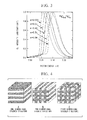
- FIG. 3 shows a change of exciton luminescence peak in accordance with the change of 13 CH 4 gas concentration (x) during growing the diamond. Observation of exciton luminescence peak was performed by a cathode luminescence method. The sample was excited by an electron beam of 13kV in an acceleration voltage and 2 ⁇ A in a beam current. The temperature of the sample was 80K.
- the mixing ratio of the 12 CH 4 gas and 13 CH 4 gas was controlled using a mass flow controller.
- the raw material gasses of the controlled flow rates controlled by the mass flow controllers were mixed by a manifold before being introduced into the synthesis chamber, and were introduced into the synthesis chamber in a desired mixing ratio.
- exciton luminescence peak accompanying the change of band-gap changes reliably in accordance with controlling the desired gas mixing ratio. This result means that the band-gap can be tuned by controlling the compositional ratio of the carbon isotopes.
- a multi-layered (plural-layered) structure having a desired barrier height, a desired barrier interval, and a desired number of repeated stacking (layering) with a considerable degree of freedom.
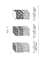
- a p-type diamond or a n-type diamond can be freely formed by introducing impurities into the environment of diamond film growth. While the above-description mainly relates to a type I super lattice structure, a two-dimensional or three-dimensional stacked structure of a diamond as shown in FIG. 4 can be realized by a production method utilizing a semiconductor processing.
- dark portions represent 13 C diamonds and white portions represent 12 C diamonds in the figures.
- FIGS. 5A, B, C each schematically shows a stacked structure of 12 C diamond film and 13 C diamond film produced in Examples 1 to 4.
- 1 denotes 13 C diamond film
- 2 denotes 12 C diamond film
- 3 denotes a high-pressure high-temperature synthesized diamond used as the substrate.
- Example 2 a high-pressure high-temperature synthesized single crystalline diamond plate having a surface of (001) crystallographic plane was used as a substrate.
- stacked (layered) body having a structure shown in FIG. 5A was produced.
- a magnetron having a maximum power output of 1.5kW, and a frequency of 2.45GHz was used as the micro-wave power supply.
- surface contaminants were removed by performing heat-cleaning using peroxide water, fluoric acid cleaning, ultra-sonic cleaning using an organic solvent, and boiling cleaning using ultra-pure water.
- the cleaned diamond plate was set on a stage in the reaction chamber.
- the interior of the chamber was maintained at a vacuum conditions in the order of 10 -8 Torr.
- pressure of residual carbonaceous gas was in the order of 10 -9 Torr or not higher than the detection limit.
- the substrate was maintained at 800°C for at least 5 hours while flowing the hydrogen gas purified by the above-described hydrogen purification so as to remove the residual carbonaceous gas in the reaction chamber.
- the above-described gasses were mixed uniformly while controlling the flow rate of each gas by the mass flow controller, and the mixed gas was introduced as a gas shower into the chamber from a shower head placed in an upper part of the reaction chamber.
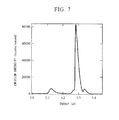
- FIG. 7 shows the results.
- an electron beam of 13 kV in acceleration voltage and 2 ⁇ A was used.
- the observation temperature of the luminescence spectrum was 80K.
- the penetration length (observation depth) of the electron beam was 1.4 ⁇ m. As it can be seen in the schematic figure, clear luminescence from excitons was observed.
- the structure of the crystal was constituted by assembled 12 C diamond films and 13 C diamond films as apparently shown in FIG. 6A , as shown in the peak position, the luminescence spectrum shown in FIG. 7 was only observed in the luminescence from the 12 C diamond film.
- This result shows that the carrier-recombination region is limited to 12 C diamond film and ensures a presence of "carrier confinement effect" which is one of characteristic properties of a super-lattice.
- the generated carrier is accumulated in the 12 C diamond film. Since the carrier is accumulated in the semiconductor layer constituting the well, recombination probability increases compared to the free space. The effective recombination results in increase of luminescence intensity.
- FIG. 8 is a schematic drawing that shows the above-explained phenomena.
- 1 and 2 shows a 13 C diamond film and a 12 C diamond film respectively.
- 4 shows a flow of carriers.
- 5 and 6 represents an electron and a hole.
- 7 and 8 denotes an exciton and a recombination luminescence process from the 12 C diamond film respectively.
- FIG. 9A shows plotting of intensities of cathodeluminescence emitted from excitons when the electron beam of the same excitation conditions is radiated to each of the samples.
- natural-C denotes a diamond synthesized using CH 4 gas which were not isotope purified.
- 12 C denotes a 12 C diamond film
- ( 12 C 13 C)n denotes a sample having a structure shown in FIG. 5A .
- integrated intensity of luminescence from natural-C was set at 1, and relative variations from this sample are shown in the figure.
- luminescence intensity was improved nearly one order in the ( 12 C 13 C)n sample having a layered structure shown in FIG. 5A .
- An isotope diamond stacked body having a structure shown in FIG. 5B was produced using conditions similar to Example 1 except for a duration of synthesis based on the growth rate calculated from FIG. 6 .
- the thus obtained diamond films respectively had film thicknesses of 875 nm, 350 nm, and 1750 nm from the upper side.
- the structure of FIG. 5A obtained in Example 1 is a multi-layered (or quantum well) structure
- the structure of Example 2 is a single-stacking (or quantum well) structure.
- FIG. 9B shows a result of Example 2. As it can be seen in FIG. 9B , photo-amplification effect can be confirmed in the "( 13 C 12 C 13 C)" structure shown in FIG. 5B as in the structure of FIG. 5A . Since this structure has a simple constitution, it can be used as a test structure for controlling an optimum barrier height and an optimum barrier interval.
- An isotope diamond stacked body having a structure shown in FIG. 5B was produced in a similar manner as in Example 2, whereas the substrate temperature was set at 900°C, the micro-wave power was 1200W, the total gas pressure was 80 Torr, the total gas flow rate was 100 SCCM, and hydrogen/methane mixing ratio was 1.2%.
- the thus obtained diamond films respectively had film thicknesses of 875 nm, 350 nm, and 1750 nm from the upper side.
- photo-amplification effect was confirmed. From this result, it can be understood that the present invention is not restricted by the synthetic conditions.
- FIG. 10 shows a result of Example 3, and shows change of spectrum in A and change of luminescence in B. As it is understood from FIG. 10A , two peaks were observed in the spectrum. The peak of low energy peak position is attributed to 12 C diamond film, and the peak of high energy peak position is attributed to the luminescence from the 13 C diamond film.
- the result shows that recombination luminescence also occurs also in the 13 C diamond film, probably caused by diffusion length of carrier generated by the electron beam excitation.
- the luminescence intensity per unit amount was amplified to 2 fold only by forming the structure of FIG. 5C .
- the results show that even in the structure of FIG. 5C where one of the 12 C diamond film is in vacuum level, the effect of the present invention is effective. That is, if an unit structure has a structure of FIG. 5C , and a state of one of the 12 C diamond film constitute a barrier for carriers, the present invention is not limited to a material to be joined.
- Isotope purification of semiconductor materials other than carbon still remains a subject of laboratory research, and requires very difficult processes for obtaining the isotope purified materials.
- carbon isotopes are already used in many fields such as medical care, environmental research, archeological dating and the like. Because of development of measuring techniques and purification techniques, it is easy to obtain carbon isotope materials of specifically high purity. Therefore, the present invention utilizing isotope diamonds constituted of carbon, has overwhelming advantages for industrial applications in the context of a supply of raw materials.
Landscapes
- Chemical & Material Sciences (AREA)
- Engineering & Computer Science (AREA)
- Materials Engineering (AREA)
- Metallurgy (AREA)
- Organic Chemistry (AREA)
- General Chemical & Material Sciences (AREA)
- Chemical Kinetics & Catalysis (AREA)
- Mechanical Engineering (AREA)
- Crystallography & Structural Chemistry (AREA)
- Inorganic Chemistry (AREA)
- Crystals, And After-Treatments Of Crystals (AREA)
- Chemical Vapour Deposition (AREA)
Abstract
Description
- The present invention relates to a stacked body of isotope diamond and a method of producing the same.
- Development of crystal growth technology has realized new semiconductor devices based on new physical concepts. One of the remarkable crystal designing technology is related to a semiconductor super-lattices constituted of different semiconductor materials alternately stacked in planer ( one dimensional ), linier (two dimensional), or blocked (three dimensional) arrangement. An important concept of this technology is in that electric structure of a crystal can be modulated by stacking two layers of semiconductor materials having different band-gap, or by forming a periodic structure in which the two-layered structure as a unit structure is repeated. Recently, attention has been paid to using a super lattice having a periodic structure of artificially developed potential as a confining technology for overcoming limits on the properties of semiconductor materials. Practically, the super-lattice is a crystal formed by artificially stacking different semiconductor materials each having a layer thickness of mono-atomic thickness to several 10s nm (typically, about 50 nm) to provide a long-range periodical structure. Numerous physical phenomena which are not shown by a bulk single crystal are observed in the super-lattice, providing various fundamental problems not only in the field of physics, but also in the field of application.
- In many cases, crystals of one dimensional super-lattice structure (hereafter, referred to as a super lattice structure or a super lattice) are classified to type I, type I', and type II in accordance with their characteristics of energy band-gap structures. Therefore, the following explanation is based on this classification.
Each ofFIGS. 1(a) to (c) shows a super-lattice of type I, type I', and type II respectively. In each figure, Ec and Ev respectively denote conduction band and valence band.
In type I and type I', conduction band and valence band of each of twosemiconductors semiconductor 1 and AlxGa1-xAs is used insemiconductor 2. As a representative stacked structure of type I' super lattice, there exists a structure in which In1-xGaxAs and GaSb1-yAsy are used insemiconductor 1 andsemiconductor 2 respectively. On the other hand, in a type II super lattice, valence band of a semiconductor overlaps the conduction band of the other semiconductor. As a representative stacked structure of this type super lattice, there exists a structure in which InAs is used as thesemiconductor 1 and GaSb is used as thesemiconductor 2. - As an alternative to the above described ΔEc and ΔEv that denote discontinuities of energy bands in conduction band and valence band, electronic state of a super lattice may be characterized by another parameters. For example, electronic state of type I super-lattice may be approximately expressed by a square-well potential as shown in
FIG. 2 . In this case, the electronic state depends on four parameters shown by with Lw of the well and with LB of the barriers.
For example, where LW and LB are each controlled to be a similar level as de Bloglie wavelength of an electron (for example, in GaAs-AlxGa1-xAs, LW may be controlled to be 30 nm or less, and LB may be controlled to be 10 nm or less), periodic potential longer than usual lattice spacing is introduced into a crystal, and a mini-band is formed. As a result, the role of the quantum effect is shown remarkably. For example, electrons can transmit (propagate) in a material with high mobility. Such electrons are actually used in some devices. A representative device is a High Electron Mobility Transistor (HEMT). In this device, secondary electron gas having extremely high mobility is formed in the layers ofsemiconductor 1 by a modulation doping super lattice structure in which doping (for example introduction of n-type dopant) is performed only in the layers ofsemiconductor 2 of a type I super lattice. In general, an active layer for transmitting electron current includes impurities for ensuring a conduction, but the impurities act as the the dominant scattering factor that suppresses the mobility of electrons. However, since an electron fallen in the well of thesemiconductor 1 is spatially separated from the impurities, the electrons hardly suffer scattering by the impurities, and mobility is largely improved, enabling actual use. Especially, in accordance with recent remarkable spreading of mobile information instruments and increasing data volume and signaling speed for wireless communication by the instruments, there is a demand for HEMT that enables high electric power conversion and high frequency operation. Currently, a HEMT utilizing a wide band-gap semiconductor is paid attention to as a device by which high-temperature, high-current, and high withstand voltage operation, and GaN-AlGaN based HEMT is proposed as an alternative to the conventional GaAs-AlGaAs based HEMT. - On the other hand, where LB is controlled to be sufficiently larger than LW, it is possible to form a single-well state that confine carriers in a desired semiconductor layer. This is due to a carrier trapping effect utilizing an energy barrier caused by the difference in band-gaps, and is one of the main characteristics of a super-lattice. A quantum-well laser is a representative example. For example, in the quantum-well laser, shortening of wavelength of laser oscillation, improvement of thermal variation of threshold current density, and enhancement of luminous efficiency are realized along with reduction of LW (for example, GaAs layer is reduced from 20 nm in type I GaAs-AlxGa1-xAs).
- However, since different species of semiconductors having different lattice constants are joined in the above-described hetero-structured super-lattice, it is impossible to avoid the introduction of defects and strains caused by mismatching the lattice constants. Recently, a super-lattice composed of the same element utilizing isotopes of Si is proposed as an alternative (see
Patent References 1 to 3, Non-Patent Reference 1). - Patent Reference 1: Japanese Unexamined Patent Application, First Publication No.
2000-26974 - Patent Reference 2: Published Japanese Translation No.
H11-500580 - Patent Reference 3: Japanese Unexamined Patent Application, First Publication, No.
H11-297624 - Non Patent Reference 1: Applied Physics Letters 83, 2318 (2003) "Growth and characterization of 28Sin/38Sin isotope superlattices".
- Currently, thin film crystallization technology, for example, by Molecular Beam Epitaxy (MBE) or Organometallic Vapor Phase Epitaxy (OMVPE) using organic metals is used in realization of a super lattice structure. In this technology, it is possible to lower the growth rate, and control the film thickness effectively. Further, this technology has an advantage of forming a steep composition profile and impurity profile, since starting and stopping of crystal growth may be controlled by a shutter. Another advantage is an capability of growing various materials. However, semiconductors constituting the super-lattice is practically made of monoatomic layer or a layer of up to several tens of nm in thickness. Therefore, epitaxial growth of high precision in the atomic order is practically required so as to realize precise periodic structure constituted of many tenth layers of those semiconductors. That is, there is increasing demand for suppressing disorder caused by fluctuation and/or strain of layer interface, crystal defects, and heterogeneity in structure so as to achieve optimum device performance by the quantum effect and trapping effect of the super lattice. Further, since the super-lattice realized by chemical compounds such as GaAs has a hetero-structure, it is impossible to avoid an introduction of defects and strains caused by mismatching of lattice constants along with introduction of crystal defects caused by non-stoichiometric composition.
- Super-lattice structures utilizing isotopes of single elements, for example, 28(Si)n30(Si)n or 70(Ge)n74(Ge)n, are proposed for solving the above-described problems. However, at preset, carrier confinement effect utilizing an energy barrier caused by difference in band-gaps has not been observed because of small relative difference between the band-gaps achieved by the isotope effect, for example, 0.36 meV in Ge and 1 meV in Si. That is, it is difficult to obtain the super-lattice effect to sufficiently take an advantage of the barrier effect simultaneously.
- Currently, the super-lattice structure is mainly realized of semiconductor materials such as GaAs, InSb, Si, and GaN. To overcome the limit of physical properties specific to the material, replacement of the material is required. For example, in Si and GaAs which are semiconductor materials used in core technologies of current electronic and optoelectronic field, upper limit of operation temperature of a device is limited to about 200°C because of constraint by the band-gap. Therefore, recent enhancement of integration and operation speed of devices reaches the limit because of thermal constraint on the physical properties. Although an application of wide-gap semiconductor of GaN may be expected, the temperature increase of the operation channel by calorification still remains a main problem.
- Based on the consideration of the above-described problems, an object of the present invention is to obtain a high performance device which is not restricted by conventional concept of a super lattice and overcomes or loosen limitations on physical properties of materials and problems concerning hetero-junction. Specifically, an object of the present invention is to provide a device in which a desired barrier height, a barrier width, a barrier interval, the numbers of repetitions of stacked layers, or crystal shape are freely controlled such that the device has a desired performance.
- As a result of extensive study to achieve the above-described object, the inventors reached the following findings. A fundamental constitution of a high performance device that overcomes or loosen imitation on physical properties of materials and problems concerning hetero-junction can be provided by constituting the main carrier generation region, or a carrier passage and an operation/non-operation channel of an isotope diamond (hereafter, referred to as 12C diamond) synthesized from carbon isotope 12C and the isotope diamond (hereafter, referred to as 13C diamond) synthesized from carbon isotope 13C, providing a junction-interface utilizing an energy barrier (quantum barrier) caused by difference in band-gaps formed by quantum effects of the 12C diamond and the 13C diamond.
While the term "super-lattice" is used in the description of the back ground art, the super-lattice denotes a crystal lattice that is formed by stacking of plural species of crystal lattices and has a periodic structure different from that of basic unit lattices. On the other hand, the effect achieved by the present invention appears even though the basic unit lattice structure in nanometer scale is not changed. Therefore, the structure including the present invention is hereafter referred to as a stacked structure. - The present invention was completed based on the above-described findings and provides the following aspects.
- [1] A stacked (layered, laminated) body of isotope diamonds, including a 13C film composed of carbon isotope 13C and a 12C film composed of carbon isotope 12C grown on a substrate by epitaxial growth, wherein the stacked body at least has a structure in which the 12C film is grown on the 13C film.
- [2] A stacked body of isotope diamonds as described in [1], wherein a thickness of the 12C film and the 13C film is mono-atomic layer thickness to 350 nm or more.
- [3] A stacked body of isotope diamonds as described in the above [1] or [2], wherein the 12C film and the 13C film are alternately stacked plural times.
- [4] A stacked body of isotope diamonds as described in the above [3], wherein a thickness of the 12C film and a thickness of the 13C film are substantially the same.
- [5] A stacked body of isotope diamonds as described in any one of the above [1] to [4], wherein the substrate is a diamond substrate.
- [6] A stacked body of isotope diamonds as described in any one of the above [1] to [5], wherein the diamond substrate is made of a single crystalline diamond, and the epitaxial growth is homo-epitaxial growth.
- [7] A method of epitaxially growing a 13C film composed of carbon isotope 13C and a 12C film composed of carbon isotope 12C on a substrate by CVD method using isotope-refined raw material gases, including performing removal of a residual gas containing unnecessary carbon from an interior of a reaction chamber by a flow of highly purified hydrogen gas and heating of the substrate, wherein the removal of the residual gas is performed before forming the films, and in the time of changing the isotope-refined raw material gas.
- According to the present invention, it is possible to achieve considerable degree of freedom in forming a desired barrier height, a desired barrier interval, desired numbers of repetitions of stacking(layering), or a desired crystal shape. Therefore, by a replacing the conventional material by isotope diamond while maintaining the conventional device structure, it is possible to provide a photo-luminescent device having high photo-luminescence efficiency and a photo-detecting (light-receiving) device having high light-detection efficiency, where a device performance is improved one or two or more orders compared to the conventional device. Further, the present invention can be applied variously. For example, it is possible to realize ultra-high speed and a low noise high-frequency device, an ultra-high current density power device or the like by applying the present invention to a channel region of a electric field effect transistor (e.g., HEMT, JFET, MESFET or the like) or a drift layer of a power device. Specifically, there is an advantage in that a thermal design (heat design) of a device can be eased automatically by excellent heat conduction of diamonds.
-
-
FIG. 1 shows types of a super-lattice. -
FIG. 2 shows a schematic drawing of a square-well potential. -
FIG. 3 shows a change of peak position of exciton luminescence in accordance with a change of 13CH4 gas concentration (x) during the growing of a diamond. -
FIG. 4 is a schematic drawing of stacked structures. -
FIG. 5 shows schematic drawings of stacked structures composed of 12C diamond films and 13C diamond films produced in Examples 1 to 3. -
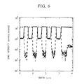
FIG. 6 shows an evaluation of the composition of isotope diamonds obtained in Example 1. -
FIG. 7 shows an evaluation of electronic states of isotope diamonds obtained in Example 1. -
FIG. 8 is a schematic drawing of carrier accumulation. -
FIG. 9 shows a change of cathode-luminescence intensity from stacked bodies of isotope diamonds obtained in Examples 1 and 2. -
FIG. 10 shows a change of cathode luminescence and luminescence intensity from a prime unit stacked structure of isotope diamonds obtained in Example 3. -
- 1:
- 13C diamond film
- 2:
- 12C diamond film
- 3:
- high-pressure high-temperature synthesized diamond
- 4:
- Flow of carriers
- 5:
- Electron
- 6:
- Hole
- 7:
- Exciton
- 8:
- Process of recombination-luminescence from a 12C diamond film.
- Next, the present invention is explained in detail.
An isotope diamond stacked body according to the present invention is a stacked body of isotope diamonds, including a 13C film composed of carbon isotope 13C and a 12C film composed of carbon isotope 12C grown on a substrate by epitaxial growth, wherein the stacked body at least has a structure in which the 12C film is grown on the 13C film.
The reason for overcoming a limitations on physical properties of material by the isotope diamond stacked body of the present invention can be clearly explained with regard to the physical properties of diamonds. Practically, a diamond has a strong chemical inactivity and resistance at room temperature. Hardness, heat conductivity, and sonic propagation speed in a crystal of the diamond is the highest and the friction coefficient is the lowest among the existing materials. In addition, the tuning range of a band-gap caused by the isotope effect of a diamond shows a relatively large value of 19 meV. Further, the thermal expansion coefficient of the diamond is comparative to the thermal expansion coefficient of a silica glass which is the lowest among the existing materials. The diamond has high dielectric break-down strength and low permittivity. An extreme difference in carrier mobility between electrons and holes as shown in a GaAs is not observed and high speed symmetrical mobility is observed in a diamond. Figure of merit (performance index) combining values of those physical properties is proposed in an application of a device. For example, the Johonson index is used as a figure of merit of a high power high frequency device. The Johonson index of a diamond is 46656 times that of Si, and 49 times that of GaN. Further, diamond also shows high performance in other semiconductor properties. For example, diamond has low permittivity and high heat conductivity. These properties are directly required for increasing an integration density and operation speed of a device. The Keyes index representing the performance of a high-density high-speed device is relatively higher when diamond is used compared to other semiconductor materials. In the Keyes index, diamond shows a possibility of device performance of 33 times that of Si, 7 times that of 4H-SiC, and 19 times that of GaN. That is diamond has a performance remarkably surpassing the performance of other semiconductor materials. - On the other hand, an important concept of a technology for obtaining the super-lattice effect is a way to prepare a semiconductor having a tuned band-gap. In general, achievement of super-lattice structure is tried by forming layered junction of semiconductors of hetero-species having an optimized thickness in the range of mono-atomic thickness to several tens of nm. Different from such junction, the present invention intends to realize a junction of semiconductors of homo-species using isotope diamonds. Technology for synthesizing 12C diamond and 13C diamond is inevitable to realize such a junction.
- The substrate used in the present invention is not limited to a specific material. Diamond substrate may be preferably used. Specifically, a diamond substrate having a surface of (001), (110), (111), or (113) crystallographic plane is preferably used. The diamond substrate may be made of a single crystalline diamond or of a polycrystalline diamond. To synthesize a defect-less high quality diamond film, it is preferable to use a single crystalline diamond plate synthesized under high-pressure and high-temperature conditions as the substrate, and homo-epitaxially grow the diamond films.
- Synthesis of a diamond stacked body according to the present invention may be performed by any of chemical vapor deposition methods including micro-wave plasma CVD method (e.g., of 915MHz or 2.45MHz in frequency), hot-filament method, electron assisted method, Plasma Torche method, Electron Cyclotron Resonance method (ECR), DC discharge plasma method, RF (radio-frequency) plasma method, RF induction thermal Plasma method, DC plasma Jet method, combustion flame method or the like. Especially, where the diamond film is synthesized using a diamond growth by micro-wave plasma CVD, it is possible to control the growth of a defect-less crystal having a flatness of atomic scale which is an inevitable feature of a super-lattice structure (see "Homoepitaxial diamond film with an atomically flat surface over a large area" in Diamond and Related Materials 8 (1999), 1272-1276).
- In the following, a method of producing a diamond stacked body of the present invention using micro-wave plasma CVD method is explained.
A micro-wave plasma CVD apparatus having a reaction chamber made of stainless steel is used in the production of diamond stacked bodies according to the present invention. The apparatus is mainly constituted of a micro-wave power supply, a reaction chamber, a raw material gas supplying unit, and an evacuation unit. - A raw material gas for producing the isotope diamond stacked body of the present invention may be selected from any gas containing carbon, for example, methane gas, carbon dioxide, carbon monoxide or the like. In general, methane gas (CH4) is used as the raw material. By modifying the CH4 to 12CH4 gas and 13CH4 gas each having isotope purified carbon (C), it is possible to realize an isotope-purified isotope diamond film. Commercially available high purity hydrogen gas and isotope-purified high purity methane gas are used as raw materials. Hydrogen gas having a purity level of 9N is used so as to suppress influence of residual carbon in the hydrogen gas that constitutes the main part of the raw materials. Residual impurities such as carbon monoxide (CO), carbon dioxide (CO2), hydrocarbon (e.g., CH4) or the like have been removed from the hydrogen gas of this level.
- After removing a surface contaminant from a substrate and setting the substrate in the reaction chamber, the substrate is heated and maintained at a predetermined temperature while flowing the purified hydrogen gas in order to remove the residual carbonaceous (carbon-containing) gas in the reaction chamber. After that, by introducing the raw material gas, a 12C diamond film and a 13C diamond film are stacked alternately. When the isotope gas is changed to form the stacked structure, residual carbonaceous gas in the reaction chamber is removed by the above-described flow of highly purified hydrogen gas and heating of the substrate without removing the substrate from the reaction chamber.
- The thickness of the film is controlled by controlling the duration (time) of the synthesis in accordance with the preliminary monitored growth rate.
The tuning of the band-gap in the isotope diamond is performed by controlling a mixing ratio of 12CH4 gas and 13CH4 gas as raw materials of the diamond utilizing an isotope effect determined by isotope ratio in the crystal.
FIG. 3 shows a change of exciton luminescence peak in accordance with the change of 13CH4 gas concentration (x) during growing the diamond. Observation of exciton luminescence peak was performed by a cathode luminescence method. The sample was excited by an electron beam of 13kV in an acceleration voltage and 2 µA in a beam current. The temperature of the sample was 80K. The mixing ratio of the 12CH4 gas and 13CH4 gas was controlled using a mass flow controller. The raw material gasses of the controlled flow rates controlled by the mass flow controllers were mixed by a manifold before being introduced into the synthesis chamber, and were introduced into the synthesis chamber in a desired mixing ratio.
As it is understood fromFIG. 3 , exciton luminescence peak accompanying the change of band-gap changes reliably in accordance with controlling the desired gas mixing ratio. This result means that the band-gap can be tuned by controlling the compositional ratio of the carbon isotopes. - By the above-explained technology, it is possible to form a multi-layered (plural-layered) structure having a desired barrier height, a desired barrier interval, and a desired number of repeated stacking (layering) with a considerable degree of freedom. In addition, based on the above-described fundamental procedure, a p-type diamond or a n-type diamond can be freely formed by introducing impurities into the environment of diamond film growth.
While the above-description mainly relates to a type I super lattice structure, a two-dimensional or three-dimensional stacked structure of a diamond as shown inFIG. 4 can be realized by a production method utilizing a semiconductor processing. Here, for example, dark portions represent 13C diamonds and white portions represent 12C diamonds in the figures. For example, there is a method for processing a one-dimensionally stacked structure in a ridge-like or mountain-like form using lithography, etching, or the like. By using such process, it is possible to form a two-dimensional or three-dimensional stacked structure in a desired form. - Next, the present invention is explained further in detail based on the Examples. It should be noted that the present invention is not limited to the examples described below.
FIGS. 5A, B, C each schematically shows a stacked structure of 12C diamond film and 13C diamond film produced in Examples 1 to 4. In thefigure, 1 denotes 13C diamond film, 2 denotes 12C diamond film, and 3 denotes a high-pressure high-temperature synthesized diamond used as the substrate. - In the Example, a high-pressure high-temperature synthesized single crystalline diamond plate having a surface of (001) crystallographic plane was used as a substrate. Using an end-lauch type micro-wave plasma CVD apparatus having a reaction chamber made of a stainless steel, stacked (layered) body having a structure shown in
FIG. 5A was produced. A magnetron having a maximum power output of 1.5kW, and a frequency of 2.45GHz was used as the micro-wave power supply.
Before setting the diamond plate in the reaction chamber, surface contaminants were removed by performing heat-cleaning using peroxide water, fluoric acid cleaning, ultra-sonic cleaning using an organic solvent, and boiling cleaning using ultra-pure water. Highly pure commercial level hydrogen gas and isotope purified high purity methane gas were used as raw material gasses. Just before mixing the hydrogen gas with the methane gas, the hydrogen gas was purified to the hydrogen gas having a purity level of 9N by removing residual impurities such as carbon monoxide (CO), carbon dioxide gas (CO2), hydrocarbon (e.g., CH4) or the like using a hydrogen defecator utilizing a chemical absorption process by a platinum catalyst. - The cleaned diamond plate was set on a stage in the reaction chamber. The interior of the chamber was maintained at a vacuum conditions in the order of 10-8 Torr. By using a potentiometer, it was confirmed that pressure of residual carbonaceous gas was in the order of 10-9 Torr or not higher than the detection limit.
Next, before depositing the diamond film, the substrate was maintained at 800°C for at least 5 hours while flowing the hydrogen gas purified by the above-described hydrogen purification so as to remove the residual carbonaceous gas in the reaction chamber.
After that, the above-described gasses were mixed uniformly while controlling the flow rate of each gas by the mass flow controller, and the mixed gas was introduced as a gas shower into the chamber from a shower head placed in an upper part of the reaction chamber. Under the conditions of a substrate temperature of 800°C, a micro-wave power of 750W, a total gas pressure of 25 Torr, a total gas flow rate of 400 SCCM, and a mixing ratio of hydrogen/methane of 0.15%, 12C diamond films and 13C diamond films were deposited alternately. At that time, mixing ratio of the gas was controlled such that hydrogen constituted 99.85% of the mixed gas, and methane constituted the rest of 0.15%.
When the isotope gas was changed to form the stacked structure, residual carbonaceous gas in the reaction chamber was removed by the flow of highly purified hydrogen gas and heating of the substrate without removing the substrate from the reaction chamber. - To examine the stacked structure of diamond obtained in Example 1, crystal composition of the thus obtained sample was measured using Secondary Ion Mass Spectroscopy (SIMS). The result is shown in
FIG. 6 . In the SIMS measurement, O2+ ion beam accelerated to 5.5 kV was irradiated to the sample surface. In the figure, solid liner denotes 12C diamond films, and the dotted line denotes 13C diamond film.
As it can be seen inFIG. 6 , a stacked structure of 12C diamond films and 13C diamond films each having a thickness of 350 nm was realized. - According to the present invention, in the 12C diamond film having relatively smaller band-gap compared to the 13C diamond film, as shown in
FIG. 3 , it was possible to form quantum-well state which was capable of confining carriers in the semiconductor layer.
Therefore, the electronic state of a structure ofFIG. 5A was examined by evaluation using a cathodeluminescence method.FIG. 7 shows the results. In the observation of luminescence spectrum, an electron beam of 13 kV in acceleration voltage and 2 µA was used. The observation temperature of the luminescence spectrum was 80K. The penetration length (observation depth) of the electron beam was 1.4 µm.
As it can be seen in the schematic figure, clear luminescence from excitons was observed. At that time, although the structure of the crystal was constituted by assembled 12C diamond films and 13C diamond films as apparently shown inFIG. 6A , as shown in the peak position, the luminescence spectrum shown inFIG. 7 was only observed in the luminescence from the 12C diamond film. This result shows that the carrier-recombination region is limited to 12C diamond film and ensures a presence of "carrier confinement effect" which is one of characteristic properties of a super-lattice. By generating carriers in the stacked structure by excitation (using photo-radiation, electron beam, radiant ray, x ray, charged particles, electric field or the like) from the outside, the generated carrier is accumulated in the 12C diamond film. Since the carrier is accumulated in the semiconductor layer constituting the well, recombination probability increases compared to the free space. The effective recombination results in increase of luminescence intensity. -
FIG. 8 is a schematic drawing that shows the above-explained phenomena. In thefigure, 1 and 2 shows a 13C diamond film and a 12C diamond film respectively. 4 shows a flow of carriers. 5 and 6 represents an electron and a hole. 7 and 8 denotes an exciton and a recombination luminescence process from the 12C diamond film respectively. -
FIG. 9A shows plotting of intensities of cathodeluminescence emitted from excitons when the electron beam of the same excitation conditions is radiated to each of the samples. In this figure, "natural-C" denotes a diamond synthesized using CH4 gas which were not isotope purified. "12C" denotes a 12C diamond film, and "(12C13C)n" denotes a sample having a structure shown inFIG. 5A . For comparison, integrated intensity of luminescence from natural-C was set at 1, and relative variations from this sample are shown in the figure. As shown in the figure, compared to the natural-C sample having natural isotope abundance ratio, and 12C diamond film sample, luminescence intensity was improved nearly one order in the (12C13C)n sample having a layered structure shown inFIG. 5A . - An isotope diamond stacked body having a structure shown in
FIG. 5B was produced using conditions similar to Example 1 except for a duration of synthesis based on the growth rate calculated fromFIG. 6 . The thus obtained diamond films respectively had film thicknesses of 875 nm, 350 nm, and 1750 nm from the upper side. While the structure ofFIG. 5A obtained in Example 1 is a multi-layered (or quantum well) structure, the structure of Example 2 is a single-stacking (or quantum well) structure.
FIG. 9B shows a result of Example 2. As it can be seen inFIG. 9B , photo-amplification effect can be confirmed in the "(13C12C13C)" structure shown inFIG. 5B as in the structure ofFIG. 5A . Since this structure has a simple constitution, it can be used as a test structure for controlling an optimum barrier height and an optimum barrier interval. - An isotope diamond stacked body having a structure shown in
FIG. 5B was produced in a similar manner as in Example 2, whereas the substrate temperature was set at 900°C, the micro-wave power was 1200W, the total gas pressure was 80 Torr, the total gas flow rate was 100 SCCM, and hydrogen/methane mixing ratio was 1.2%. The thus obtained diamond films respectively had film thicknesses of 875 nm, 350 nm, and 1750 nm from the upper side. Like as the structure ofFIG. 5A and FIG. 5B , photo-amplification effect was confirmed. From this result, it can be understood that the present invention is not restricted by the synthetic conditions. - An isotope diamond stacked body having a structure shown in
FIG. 5C was produced using conditions similar to Example 1 except for a duration of synthesis based on the growth rate calculated fromFIG. 6 . The thus obtained diamond films each had film thicknesses of 350 nm, and 3150 nm from the upper side.
FIG. 10 shows a result of Example 3, and shows change of spectrum in A and change of luminescence in B. As it is understood fromFIG. 10A , two peaks were observed in the spectrum. The peak of low energy peak position is attributed to 12C diamond film, and the peak of high energy peak position is attributed to the luminescence from the 13C diamond film. The result shows that recombination luminescence also occurs also in the 13C diamond film, probably caused by diffusion length of carrier generated by the electron beam excitation. However, as shown inFIG. 10 , compared to the free space of 12C diamond film (sample type 12C), the luminescence intensity per unit amount was amplified to 2 fold only by forming the structure ofFIG. 5C . The results show that even in the structure ofFIG. 5C where one of the 12C diamond film is in vacuum level, the effect of the present invention is effective. That is, if an unit structure has a structure ofFIG. 5C , and a state of one of the 12C diamond film constitute a barrier for carriers, the present invention is not limited to a material to be joined. - Isotope purification of semiconductor materials other than carbon still remains a subject of laboratory research, and requires very difficult processes for obtaining the isotope purified materials. On the other hand, carbon isotopes are already used in many fields such as medical care, environmental research, archeological dating and the like. Because of development of measuring techniques and purification techniques, it is easy to obtain carbon isotope materials of specifically high purity. Therefore, the present invention utilizing isotope diamonds constituted of carbon, has overwhelming advantages for industrial applications in the context of a supply of raw materials.
Application of diamond semiconductor to a power device requiring high temperature, high current, and high dielectric strength operation, high speed transistors, high frequency devices, deep ultraviolet ray emitting devices, ultraviolet ray detecting devices, superconductor devices, radiant ray detectors, biosensor, quantum computing devices and the like is currently studied. The present invention provides the principal concept of realizing such next-generation semiconductor materials composed of diamond, and enhances its industrial application.
Claims (7)
- A stacked body of isotope diamonds, comprising a 13C film composed of carbon isotope 13C and a 12C film composed of carbon isotope 12C grown on a substrate by epitaxial growth, wherein the stacked body at least has a structure in which the 12C film is grown on the 13C film.
- A stacked body of isotope diamonds according to claim 1, wherein a thickness of the 12C film and the 13C film is monoatmic layer thickness to 350 nm or more.
- A stacked body of isotope diamonds according to claims 1 or 2, wherein the 12C film and the 13C film are alternately stacked plural times.
- A stacked body of isotope diamonds according to claim 3, wherein a thickness of the 12C film and a thickness of the 13C film are substantially the same.
- A stacked body of isotope diamonds according to any one of claims 1 to 4, wherein the substrate is a diamond substrate.
- A stacked body of isotope diamonds according to any one of claims 1 to 5, wherein the diamond substrate is made of a single crystalline diamond, and the epitaxial growth is homo-epitaxial growth.
- A method of producing a stacked body of isotope diamond according to claim 1, including epitaxially growing a 13C film composed of carbon isotope 13C and a 12C film composed of carbon isotope 12C on a substrate by CVD method using isotope-refined raw material gases, the method comprising
performing removal of a residual gas containing unnecessary carbon from an interior of a reaction chamber by a flow of highly purified hydrogen gas and heating of the substrate, wherein the removal of the residual gas is performed before forming the films, and in the time of changing the isotope-refined raw material gas.
Applications Claiming Priority (2)
| Application Number | Priority Date | Filing Date | Title |
|---|---|---|---|
| JP2007259942 | 2007-10-03 | ||
| PCT/JP2008/068091 WO2009044882A1 (en) | 2007-10-03 | 2008-10-03 | Isotope diamond laminate |
Publications (3)
| Publication Number | Publication Date |
|---|---|
| EP2196564A1 true EP2196564A1 (en) | 2010-06-16 |
| EP2196564A4 EP2196564A4 (en) | 2011-05-11 |
| EP2196564B1 EP2196564B1 (en) | 2013-03-06 |
Family
ID=40526302
Family Applications (1)
| Application Number | Title | Priority Date | Filing Date |
|---|---|---|---|
| EP08834751A Active EP2196564B1 (en) | 2007-10-03 | 2008-10-03 | Isotope diamond laminate |
Country Status (4)
| Country | Link |
|---|---|
| US (1) | US20100247884A1 (en) |
| EP (1) | EP2196564B1 (en) |
| JP (1) | JP5263893B2 (en) |
| WO (1) | WO2009044882A1 (en) |
Cited By (2)
| Publication number | Priority date | Publication date | Assignee | Title |
|---|---|---|---|---|
| WO2014079836A3 (en) * | 2012-11-21 | 2014-07-17 | Element Six Technologies Limited | Synthetic diamond heat spreaders |
| CN106024862A (en) * | 2016-06-28 | 2016-10-12 | 上海大学 | Preparation method for novel diamond film/GaN heterojunction with electrode |
Families Citing this family (4)
| Publication number | Priority date | Publication date | Assignee | Title |
|---|---|---|---|---|
| JP2013229493A (en) * | 2012-04-26 | 2013-11-07 | Sharp Corp | Group-iii nitride semiconductor stacked substrate and group-iii nitride semiconductor field-effect transistor |
| JP6098050B2 (en) * | 2012-07-02 | 2017-03-22 | 住友電気工業株式会社 | Composite polycrystalline diamond and method for producing the same |
| GB201707486D0 (en) | 2017-05-10 | 2017-06-21 | Univ Bristol | Radiation powered devices comprising diamond material |
| US10866503B1 (en) | 2019-07-26 | 2020-12-15 | Applied Materials, Inc. | Low emission implantation mask and substrate assembly |
Family Cites Families (8)
| Publication number | Priority date | Publication date | Assignee | Title |
|---|---|---|---|---|
| US5360479A (en) * | 1990-07-02 | 1994-11-01 | General Electric Company | Isotopically pure single crystal epitaxial diamond films and their preparation |
| JPH05270987A (en) * | 1992-03-27 | 1993-10-19 | Kanagawa Pref Gov | Carbon 13 isotope diamond substrate and its production |
| US5917195A (en) | 1995-02-17 | 1999-06-29 | B.A. Painter, Iii | Phonon resonator and method for its production |
| JPH11297624A (en) | 1998-04-08 | 1999-10-29 | Japan Science & Technology Corp | Thin film element and method of manufacturing the same |
| US6582513B1 (en) * | 1998-05-15 | 2003-06-24 | Apollo Diamond, Inc. | System and method for producing synthetic diamond |
| JP2000026974A (en) | 1998-07-08 | 2000-01-25 | Fujitsu Ltd | Thin film forming method and thin film forming apparatus |
| US6653212B1 (en) * | 1999-04-20 | 2003-11-25 | Sony Corporation | Method and apparatus for thin-film deposition, and method of manufacturing thin-film semiconductor device |
| JP2003051609A (en) * | 2001-08-03 | 2003-02-21 | Tokyo Gas Co Ltd | Diamond high-intensity ultraviolet light emitting element |
-
2008
- 2008-10-03 JP JP2009536120A patent/JP5263893B2/en active Active
- 2008-10-03 WO PCT/JP2008/068091 patent/WO2009044882A1/en not_active Ceased
- 2008-10-03 EP EP08834751A patent/EP2196564B1/en active Active
- 2008-10-03 US US12/681,145 patent/US20100247884A1/en not_active Abandoned
Cited By (5)
| Publication number | Priority date | Publication date | Assignee | Title |
|---|---|---|---|---|
| WO2014079836A3 (en) * | 2012-11-21 | 2014-07-17 | Element Six Technologies Limited | Synthetic diamond heat spreaders |
| GB2511156A (en) * | 2012-11-21 | 2014-08-27 | Element Six Ltd | Synthetic diamond heat spreaders |
| US9214407B2 (en) | 2012-11-21 | 2015-12-15 | Element Six Technologies Limited | Synthetic diamond heat spreaders |
| CN106024862A (en) * | 2016-06-28 | 2016-10-12 | 上海大学 | Preparation method for novel diamond film/GaN heterojunction with electrode |
| CN106024862B (en) * | 2016-06-28 | 2019-06-25 | 上海大学 | A kind of preparation method of diamond thin film/GaN heterojunction with electrode |
Also Published As
| Publication number | Publication date |
|---|---|
| EP2196564B1 (en) | 2013-03-06 |
| WO2009044882A1 (en) | 2009-04-09 |
| JPWO2009044882A1 (en) | 2011-02-10 |
| US20100247884A1 (en) | 2010-09-30 |
| JP5263893B2 (en) | 2013-08-14 |
| EP2196564A4 (en) | 2011-05-11 |
Similar Documents
| Publication | Publication Date | Title |
|---|---|---|
| US8876973B2 (en) | Film of n type (100) oriented single crystal diamond semiconductor doped with phosphorous atoms, and a method of producing the same | |
| EP2196564B1 (en) | Isotope diamond laminate | |
| He et al. | Growth and characterization of ternary AlGaN alloy nanocones across the entire composition range | |
| Yuan et al. | Synthesis, microstructure, and cathodoluminescence of [0001]-oriented GaN nanorods grown on conductive graphite substrate | |
| EP1179621A1 (en) | N-type semiconductor diamond and its fabrication method | |
| Rudder et al. | Thermal CVD of homoepitaxial diamond using CF4 and F2 | |
| Vézian et al. | Origins of GaN (0 0 0 1) surface reconstructions | |
| Almalawi et al. | Simultaneous growth strategy of high-optical-efficiency GaN NWs on a wide range of substrates by pulsed laser deposition | |
| Bae et al. | Heteroepitaxial growth of Ga2O3 thin films on nickel-nanodot-induced buffer layers for solar-blind ultraviolet photodetector applications | |
| Kato et al. | N-type doping on (001)-oriented diamond | |
| Nanishi et al. | Plasma-excited MBE—Proposal and achievements through R&D of compound semiconductor materials and devices | |
| Chen et al. | Growth and Characterization of Nonpolar Nanoporous AlN by Inward Conversion of (004) γ-LiAlO2 Crystals | |
| Wang et al. | Effects of gallium surfactant on AlN thin films by microwave plasma chemical vapor deposition | |
| US6966948B2 (en) | Method to manufacture Indium Nitride quantum dots | |
| Nilsson | Doping of high-Al-content AlGaN grown by MOCVD | |
| Mao et al. | Comparative study of the effect of H2 addition on ZnO films grown by different zinc and oxygen precursors | |
| Ma et al. | Controlled lateral epitaxial growth in vertical β-Ga2O3 nanowires on sapphire by MOCVD | |
| Kato et al. | n-Type diamond growth by phosphorus doping | |
| Wang | Epitaxial growth and characterization of hexagonal boron gallium nitride semiconductor alloys | |
| Lemettinen | Epitaxy of gallium nitride films on silicon substrates | |
| Teraji | Chemical vapor deposition of homoepitaxial diamond films | |
| Koizumi | N-type diamond growth | |
| Carrascon | Epitaxy of group III-nitride materials using different nucleation schemes | |
| Nipa | Effect of Growth Conditions on the Performance of Vertically Conducting Beta-Ga2O3 Diodes on 4H-SiC Substrate by MOCVD | |
| Abas | Indium nitride growth with in situ surface modification by RF-MBE |
Legal Events
| Date | Code | Title | Description |
|---|---|---|---|
| PUAI | Public reference made under article 153(3) epc to a published international application that has entered the european phase |
Free format text: ORIGINAL CODE: 0009012 |
|
| 17P | Request for examination filed |
Effective date: 20100412 |
|
| AK | Designated contracting states |
Kind code of ref document: A1 Designated state(s): AT BE BG CH CY CZ DE DK EE ES FI FR GB GR HR HU IE IS IT LI LT LU LV MC MT NL NO PL PT RO SE SI SK TR |
|
| AX | Request for extension of the european patent |
Extension state: AL BA MK RS |
|
| DAX | Request for extension of the european patent (deleted) | ||
| A4 | Supplementary search report drawn up and despatched |
Effective date: 20110411 |
|
| GRAP | Despatch of communication of intention to grant a patent |
Free format text: ORIGINAL CODE: EPIDOSNIGR1 |
|
| GRAS | Grant fee paid |
Free format text: ORIGINAL CODE: EPIDOSNIGR3 |
|
| GRAA | (expected) grant |
Free format text: ORIGINAL CODE: 0009210 |
|
| AK | Designated contracting states |
Kind code of ref document: B1 Designated state(s): AT BE BG CH CY CZ DE DK EE ES FI FR GB GR HR HU IE IS IT LI LT LU LV MC MT NL NO PL PT RO SE SI SK TR |
|
| REG | Reference to a national code |
Ref country code: GB Ref legal event code: FG4D |
|
| REG | Reference to a national code |
Ref country code: CH Ref legal event code: EP Ref country code: AT Ref legal event code: REF Ref document number: 599684 Country of ref document: AT Kind code of ref document: T Effective date: 20130315 |
|
| REG | Reference to a national code |
Ref country code: IE Ref legal event code: FG4D |
|
| REG | Reference to a national code |
Ref country code: DE Ref legal event code: R096 Ref document number: 602008022775 Country of ref document: DE Effective date: 20130502 |
|
| REG | Reference to a national code |
Ref country code: AT Ref legal event code: MK05 Ref document number: 599684 Country of ref document: AT Kind code of ref document: T Effective date: 20130306 |
|
| PG25 | Lapsed in a contracting state [announced via postgrant information from national office to epo] |
Ref country code: AT Free format text: LAPSE BECAUSE OF FAILURE TO SUBMIT A TRANSLATION OF THE DESCRIPTION OR TO PAY THE FEE WITHIN THE PRESCRIBED TIME-LIMIT Effective date: 20130306 Ref country code: BG Free format text: LAPSE BECAUSE OF FAILURE TO SUBMIT A TRANSLATION OF THE DESCRIPTION OR TO PAY THE FEE WITHIN THE PRESCRIBED TIME-LIMIT Effective date: 20130606 Ref country code: LT Free format text: LAPSE BECAUSE OF FAILURE TO SUBMIT A TRANSLATION OF THE DESCRIPTION OR TO PAY THE FEE WITHIN THE PRESCRIBED TIME-LIMIT Effective date: 20130306 Ref country code: SE Free format text: LAPSE BECAUSE OF FAILURE TO SUBMIT A TRANSLATION OF THE DESCRIPTION OR TO PAY THE FEE WITHIN THE PRESCRIBED TIME-LIMIT Effective date: 20130306 Ref country code: NO Free format text: LAPSE BECAUSE OF FAILURE TO SUBMIT A TRANSLATION OF THE DESCRIPTION OR TO PAY THE FEE WITHIN THE PRESCRIBED TIME-LIMIT Effective date: 20130606 Ref country code: ES Free format text: LAPSE BECAUSE OF FAILURE TO SUBMIT A TRANSLATION OF THE DESCRIPTION OR TO PAY THE FEE WITHIN THE PRESCRIBED TIME-LIMIT Effective date: 20130617 |
|
| REG | Reference to a national code |
Ref country code: NL Ref legal event code: VDEP Effective date: 20130306 |
|
| REG | Reference to a national code |
Ref country code: LT Ref legal event code: MG4D |
|
| PG25 | Lapsed in a contracting state [announced via postgrant information from national office to epo] |
Ref country code: SI Free format text: LAPSE BECAUSE OF FAILURE TO SUBMIT A TRANSLATION OF THE DESCRIPTION OR TO PAY THE FEE WITHIN THE PRESCRIBED TIME-LIMIT Effective date: 20130306 Ref country code: FI Free format text: LAPSE BECAUSE OF FAILURE TO SUBMIT A TRANSLATION OF THE DESCRIPTION OR TO PAY THE FEE WITHIN THE PRESCRIBED TIME-LIMIT Effective date: 20130306 Ref country code: GR Free format text: LAPSE BECAUSE OF FAILURE TO SUBMIT A TRANSLATION OF THE DESCRIPTION OR TO PAY THE FEE WITHIN THE PRESCRIBED TIME-LIMIT Effective date: 20130607 Ref country code: LV Free format text: LAPSE BECAUSE OF FAILURE TO SUBMIT A TRANSLATION OF THE DESCRIPTION OR TO PAY THE FEE WITHIN THE PRESCRIBED TIME-LIMIT Effective date: 20130306 |
|
| PG25 | Lapsed in a contracting state [announced via postgrant information from national office to epo] |
Ref country code: BE Free format text: LAPSE BECAUSE OF FAILURE TO SUBMIT A TRANSLATION OF THE DESCRIPTION OR TO PAY THE FEE WITHIN THE PRESCRIBED TIME-LIMIT Effective date: 20130306 Ref country code: HR Free format text: LAPSE BECAUSE OF FAILURE TO SUBMIT A TRANSLATION OF THE DESCRIPTION OR TO PAY THE FEE WITHIN THE PRESCRIBED TIME-LIMIT Effective date: 20130306 |
|
| PG25 | Lapsed in a contracting state [announced via postgrant information from national office to epo] |
Ref country code: PT Free format text: LAPSE BECAUSE OF FAILURE TO SUBMIT A TRANSLATION OF THE DESCRIPTION OR TO PAY THE FEE WITHIN THE PRESCRIBED TIME-LIMIT Effective date: 20130708 Ref country code: SK Free format text: LAPSE BECAUSE OF FAILURE TO SUBMIT A TRANSLATION OF THE DESCRIPTION OR TO PAY THE FEE WITHIN THE PRESCRIBED TIME-LIMIT Effective date: 20130306 Ref country code: EE Free format text: LAPSE BECAUSE OF FAILURE TO SUBMIT A TRANSLATION OF THE DESCRIPTION OR TO PAY THE FEE WITHIN THE PRESCRIBED TIME-LIMIT Effective date: 20130306 Ref country code: IS Free format text: LAPSE BECAUSE OF FAILURE TO SUBMIT A TRANSLATION OF THE DESCRIPTION OR TO PAY THE FEE WITHIN THE PRESCRIBED TIME-LIMIT Effective date: 20130706 Ref country code: NL Free format text: LAPSE BECAUSE OF FAILURE TO SUBMIT A TRANSLATION OF THE DESCRIPTION OR TO PAY THE FEE WITHIN THE PRESCRIBED TIME-LIMIT Effective date: 20130306 Ref country code: RO Free format text: LAPSE BECAUSE OF FAILURE TO SUBMIT A TRANSLATION OF THE DESCRIPTION OR TO PAY THE FEE WITHIN THE PRESCRIBED TIME-LIMIT Effective date: 20130306 Ref country code: CZ Free format text: LAPSE BECAUSE OF FAILURE TO SUBMIT A TRANSLATION OF THE DESCRIPTION OR TO PAY THE FEE WITHIN THE PRESCRIBED TIME-LIMIT Effective date: 20130306 |
|
| PG25 | Lapsed in a contracting state [announced via postgrant information from national office to epo] |
Ref country code: CY Free format text: LAPSE BECAUSE OF FAILURE TO SUBMIT A TRANSLATION OF THE DESCRIPTION OR TO PAY THE FEE WITHIN THE PRESCRIBED TIME-LIMIT Effective date: 20130306 Ref country code: PL Free format text: LAPSE BECAUSE OF FAILURE TO SUBMIT A TRANSLATION OF THE DESCRIPTION OR TO PAY THE FEE WITHIN THE PRESCRIBED TIME-LIMIT Effective date: 20130306 |
|
| PLBE | No opposition filed within time limit |
Free format text: ORIGINAL CODE: 0009261 |
|
| STAA | Information on the status of an ep patent application or granted ep patent |
Free format text: STATUS: NO OPPOSITION FILED WITHIN TIME LIMIT |
|
| PG25 | Lapsed in a contracting state [announced via postgrant information from national office to epo] |
Ref country code: DK Free format text: LAPSE BECAUSE OF FAILURE TO SUBMIT A TRANSLATION OF THE DESCRIPTION OR TO PAY THE FEE WITHIN THE PRESCRIBED TIME-LIMIT Effective date: 20130306 |
|
| 26N | No opposition filed |
Effective date: 20131209 |
|
| PG25 | Lapsed in a contracting state [announced via postgrant information from national office to epo] |
Ref country code: IT Free format text: LAPSE BECAUSE OF FAILURE TO SUBMIT A TRANSLATION OF THE DESCRIPTION OR TO PAY THE FEE WITHIN THE PRESCRIBED TIME-LIMIT Effective date: 20130306 |
|
| REG | Reference to a national code |
Ref country code: DE Ref legal event code: R097 Ref document number: 602008022775 Country of ref document: DE Effective date: 20131209 |
|
| PG25 | Lapsed in a contracting state [announced via postgrant information from national office to epo] |
Ref country code: MC Free format text: LAPSE BECAUSE OF FAILURE TO SUBMIT A TRANSLATION OF THE DESCRIPTION OR TO PAY THE FEE WITHIN THE PRESCRIBED TIME-LIMIT Effective date: 20130306 |
|
| REG | Reference to a national code |
Ref country code: CH Ref legal event code: PL |
|
| REG | Reference to a national code |
Ref country code: IE Ref legal event code: MM4A |
|
| PG25 | Lapsed in a contracting state [announced via postgrant information from national office to epo] |
Ref country code: LI Free format text: LAPSE BECAUSE OF NON-PAYMENT OF DUE FEES Effective date: 20131031 Ref country code: CH Free format text: LAPSE BECAUSE OF NON-PAYMENT OF DUE FEES Effective date: 20131031 |
|
| PG25 | Lapsed in a contracting state [announced via postgrant information from national office to epo] |
Ref country code: IE Free format text: LAPSE BECAUSE OF NON-PAYMENT OF DUE FEES Effective date: 20131003 |
|
| PG25 | Lapsed in a contracting state [announced via postgrant information from national office to epo] |
Ref country code: TR Free format text: LAPSE BECAUSE OF FAILURE TO SUBMIT A TRANSLATION OF THE DESCRIPTION OR TO PAY THE FEE WITHIN THE PRESCRIBED TIME-LIMIT Effective date: 20130306 |
|
| PG25 | Lapsed in a contracting state [announced via postgrant information from national office to epo] |
Ref country code: LU Free format text: LAPSE BECAUSE OF NON-PAYMENT OF DUE FEES Effective date: 20131003 Ref country code: HU Free format text: LAPSE BECAUSE OF FAILURE TO SUBMIT A TRANSLATION OF THE DESCRIPTION OR TO PAY THE FEE WITHIN THE PRESCRIBED TIME-LIMIT; INVALID AB INITIO Effective date: 20081003 |
|
| PG25 | Lapsed in a contracting state [announced via postgrant information from national office to epo] |
Ref country code: MT Free format text: LAPSE BECAUSE OF FAILURE TO SUBMIT A TRANSLATION OF THE DESCRIPTION OR TO PAY THE FEE WITHIN THE PRESCRIBED TIME-LIMIT Effective date: 20130306 |
|
| REG | Reference to a national code |
Ref country code: FR Ref legal event code: PLFP Year of fee payment: 9 |
|
| REG | Reference to a national code |
Ref country code: FR Ref legal event code: PLFP Year of fee payment: 10 |
|
| REG | Reference to a national code |
Ref country code: FR Ref legal event code: PLFP Year of fee payment: 11 |
|
| PGFP | Annual fee paid to national office [announced via postgrant information from national office to epo] |
Ref country code: GB Payment date: 20250820 Year of fee payment: 18 |
|
| PGFP | Annual fee paid to national office [announced via postgrant information from national office to epo] |
Ref country code: FR Payment date: 20250821 Year of fee payment: 18 |
|
| PGFP | Annual fee paid to national office [announced via postgrant information from national office to epo] |
Ref country code: DE Payment date: 20250820 Year of fee payment: 18 |