EP2194646A1 - Method of improving noise characteristics of an ADPLL and a relative ADPLL - Google Patents
Method of improving noise characteristics of an ADPLL and a relative ADPLL Download PDFInfo
- Publication number
- EP2194646A1 EP2194646A1 EP09177501A EP09177501A EP2194646A1 EP 2194646 A1 EP2194646 A1 EP 2194646A1 EP 09177501 A EP09177501 A EP 09177501A EP 09177501 A EP09177501 A EP 09177501A EP 2194646 A1 EP2194646 A1 EP 2194646A1
- Authority
- EP
- European Patent Office
- Prior art keywords
- tdc
- signal
- digital
- time
- word
- Prior art date
- Legal status (The legal status is an assumption and is not a legal conclusion. Google has not performed a legal analysis and makes no representation as to the accuracy of the status listed.)
- Granted
Links
Images




Classifications
-
- H—ELECTRICITY
- H03—ELECTRONIC CIRCUITRY
- H03L—AUTOMATIC CONTROL, STARTING, SYNCHRONISATION OR STABILISATION OF GENERATORS OF ELECTRONIC OSCILLATIONS OR PULSES
- H03L7/00—Automatic control of frequency or phase; Synchronisation
- H03L7/06—Automatic control of frequency or phase; Synchronisation using a reference signal applied to a frequency- or phase-locked loop
- H03L7/08—Details of the phase-locked loop
- H03L7/099—Details of the phase-locked loop concerning mainly the controlled oscillator of the loop
- H03L7/0991—Details of the phase-locked loop concerning mainly the controlled oscillator of the loop the oscillator being a digital oscillator, e.g. composed of a fixed oscillator followed by a variable frequency divider
-
- H—ELECTRICITY
- H03—ELECTRONIC CIRCUITRY
- H03L—AUTOMATIC CONTROL, STARTING, SYNCHRONISATION OR STABILISATION OF GENERATORS OF ELECTRONIC OSCILLATIONS OR PULSES
- H03L2207/00—Indexing scheme relating to automatic control of frequency or phase and to synchronisation
- H03L2207/50—All digital phase-locked loop
Definitions
- This invention relates to phase locked loops and more particularly to a method of improving noise characteristics of an all-digital phase locked loop and a relative all-digital phase locked loop.
- ADPLLs all-digital PLLs
- DCO digitally controlled oscillator
- TDC time-to-digital converter
- ADPLLs offer wide programmability, easy technology scaling, and environmental robustness, while maintaining the same input-output behavior as analog PLLs.
- the "dividerless" architecture is most attractive, because it avoids the need for a critical multimodulus divider by integrating the functions of PFD-CP/dividers (Phase Frequency Detector - Charge Pump) from a classic analog synthesizer into the TDC.
- PFD-CP/dividers Phase Frequency Detector - Charge Pump
- Fref represents the reference clock
- Fout the ADPLL output signal.
- the Frequency Control Word (FCW) defines the desired ratio between Fout and Fref.
- the TDC generates a digital word RDCO that represents the DCO output phase, and the word RR represents the reference phase.
- the divider, Phase Frequency Detector (PFD) and Charge Pump (CP) are all replaced by the TDC, which must provide a measurement of how the oscillator phase differs from the reference one.
- the TDC computes the ratio between Fout and Fref
- an integrator INTEGRATOR converts the frequency error ⁇ into a phase information, that exactly corresponds to the phase difference between the output signal and the reference signal (except for a constant phase offset arising from integration).
- a low-pass digital filter DIGITAL LPF extracts the low-pass part of the output of the integrator, that is used to control the DCO.
- the TDC depicted in FIG. 1 may be substantially composed of a simple clocked-resettable integer counter INTEGER COUNTER, characterized by a resolution equal to a whole DCO period. Significantly better ADPLL performance can be achieved if a fractional counter FRACTIONAL COUNTER is used in conjunction with it, to improve the TDC resolution whilst keeping the same dynamic range of the integer counter, as shown in FIG. 3 .
- the digital output C F [n] of the fractional counter is derived by the block 1-z -1 and is added to the output C I [n] of the integer counter to generate the digital word Fout/Fref.
- the fractional counter is used to compute the residual time distance between two reference edges after integer counting, as illustrated in the time diagram of FIG. 4 .
- the time interval Integer Count represents the result of integer counting operation (C I [n]), i.e. the number of DCO periods (periods of the continuous-time oscillating signal Fout) between two reference edges.
- the time interval Fractional Count (indicated in gray) is the result of the fractional counter computation (C F [n]), i.e. a measurement of the time distance between each reference edge and the last DCO edge.
- the residual time distance between two reference edges can be computed as C F [n]+(1-C F [n-1]), i.e. 1+(1-z -1 )C F [n], as shown in FIG. 3 (where the constant contribution is not highlighted).
- in band spurious tones [4] is clearly visible in FIG. 6 , at frequencies of about 10 6 Hz and 2 ⁇ 10 6 Hz.
- the amplitude of these tones is reduced by 30dB in the reported figure compared to the real value, due to the use of a 1kHz resolution bandwidth for the measurement [4].
- this may be done by adding a dither signal to the digital word generated by the time-to-digital converter.
- a second dither signal generated as an inverted and amplified replica of the first dither signal may be added to the digital word generated by the time-to-digital converter, in order to compensate noise introduced by delaying the reference clock or the oscillating signal by a time determined in function of the level of the first dither signal.
- variations of the digital word are measured in function of variations of the delay time in respect to a reference delay time and a look-up table is filled with the measured variations and the corresponding variations of the delay time.
- a method of generating a digital feedback word of an ADPLL and a relative feedback circuit for an ADPLL and a relative ADPLL are also disclosed.
- FIG. 5 A first embodiment aimed to cancel the spurious tones introduced at the output due to the finite resolution of the TDC (quantization) is depicted in FIG. 5 .
- the signal (a) is obtained with an integer counter alone, the signals (b) with an integer counter and an infinite resolution fractional counter, the signals (c) with an integer counter and a 4-level fractional counter.
- the finite resolution causes the ⁇ [n] signal to have periodic information, that produces spurs at the synthesizer output.
- the output C F [n] is corrupted by a dither signal such that the quantization error becomes randomized.
- a dither signal with a small amplitude, for example of about one quantization step of the TDC, either as a variable analog delay element immediately before the TDC on the reference path ( FIG. 6 ) or on the DCO path (Fout in FIG. 6 ), or in a second embodiment (not depicted) as a digital signal added to the TDC output Fout/Fref.
- a shaped dither signal is preferably used to avoid a negative impact to the in-band noise. More particularly, a dither signal whose energy increases with frequency is preferably used, such that the in-band contribution is negligible and the low-pass nature of the loop counteracts the higher noise power out of band. Independently on whether the spectral density of the dither signal is white or highpass shaped, a multi-level dither is more effective than a two-level dither.
- a multi-level dither can be done by using a programmable delay element (or any alternative means for phase programmability) with a fine delay granularity. Mismatches in the extra delay element itself do not negatively affect performances.
- the novel technique of this disclosure removes spurs due to temporal quantization inherent in the TDC, while requiring minimal hardware modifications to a TDC-based ADPLL.
- By placing a variable delay element before the TDC and providing a properly shaped dither signal, as shown in FIG. 7 minimal impact to in-band noise performance is achieved.
- a pseudorandom dither signal generated by a LFSR Linear Feedback Shift Register
- LFSR Linear Feedback Shift Register
- the novel technique of this disclosure increases the amplitude of the dither signal and uses a multi-level dither sequence and so allows reduction of spurs due to non-linearity of the TDC to below the in-band noise floor, trading for an increase of the in-band noise power.
- Another improvement consists in compensating the undesired effect of the voluntarily injected dither, that is the effect of increasing the in-band noise floor.
- the input dither is a pseudorandom sequence, it is always possible to predict the resulting injected phase error and thus to compensate it, as shown in FIG. 9 .
- the gain ⁇ relating the analog delays to the digital compensation signal is a high-resolution word, and thus can be precisely controlled.
- digitally cancelling the introduced dither using a digital feed-forward path achieves the same reduction of spurs due to both quantization and non-linearity without penalizing significantly the in-band noise power.
- a technique for an accurate estimation of the gain ⁇ used for compensation is used to make the in-band noise floor equal to that of an undithered ADPLL.
- a delay value of the additional variable delay element is chosen to be the "reference delay”.
- a different delay value to be calibrated against the "reference delay” is alternated for many samples with the "reference delay", as shown in FIG. 10 , for the simplified case of a short periodicity channel with a large number of TDC quantization levels.
- each sample is subtracted from the previous one for measuring the relative time difference between the delays in terms of TDC output values TDC OUT .
- the absolute values of the results are averaged, obtaining an accurate measurement of the relative time difference between the delays for various TDC output values.
- This preferred technique based on a digital estimation preferably executed at the start-up of the proposed ADPLL, relaxes analog precision requirements of the delay element of the embodiments disclosed hereinbefore.
- the most preferred embodiment of the proposed method is in practice a self-calibrating spur reduction method for ADPLLs with no impact to the in-band noise floor.
- the applied dither signal has a dynamic range equal to ⁇ 1 LSB of the fractional TDC ( ⁇ 8ps) and a step of 1ps (16 levels).
- the effect of white and 1 st order shaped dither on the ADPLL phase noise around the carrier is compared in FIG. 11 .
Landscapes
- Analogue/Digital Conversion (AREA)
- Stabilization Of Oscillater, Synchronisation, Frequency Synthesizers (AREA)
Abstract
Description
- This invention relates to phase locked loops and more particularly to a method of improving noise characteristics of an all-digital phase locked loop and a relative all-digital phase locked loop.
- Classical analog fractional synthesizers are generally over-constrained in the design phase by shrinking processes, reduced supply voltage and multi-standard integration.
- Essentially digital PLL architectures, such as all-digital PLLs (ADPLLs) [1-3], obviate to these limitations thanks to the intrinsically digital nature, with a digitally controlled oscillator (DCO) and a time-to-digital converter (TDC) as the sole analog blocks. As a result, ADPLLs offer wide programmability, easy technology scaling, and environmental robustness, while maintaining the same input-output behavior as analog PLLs. From a complexity standpoint, the "dividerless" architecture is most attractive, because it avoids the need for a critical multimodulus divider by integrating the functions of PFD-CP/dividers (Phase Frequency Detector - Charge Pump) from a classic analog synthesizer into the TDC. An example [5] of a dividerless architecture is depicted in FIG. l. Another known [6] dividerless architecture is depicted in
FIG. 2 . - In
FIG. 1 , Fref represents the reference clock, Fout the ADPLL output signal. The Frequency Control Word (FCW) defines the desired ratio between Fout and Fref. InFIG. 2 , the TDC generates a digital word RDCO that represents the DCO output phase, and the word RR represents the reference phase. - Compared to a classical analog PLL, the divider, Phase Frequency Detector (PFD) and Charge Pump (CP) are all replaced by the TDC, which must provide a measurement of how the oscillator phase differs from the reference one. In particular, as shown in
FIG. 1 , the TDC computes the ratio between Fout and Fref, and an integrator INTEGRATOR converts the frequency error ε into a phase information, that exactly corresponds to the phase difference between the output signal and the reference signal (except for a constant phase offset arising from integration). A low-pass digital filter DIGITAL LPF extracts the low-pass part of the output of the integrator, that is used to control the DCO. - In a practical application, however, the accuracy of such phase information is degraded by the finite resolution of the TDC, which adds a quantization noise in the ADPLL loop.
- The TDC depicted in
FIG. 1 may be substantially composed of a simple clocked-resettable integer counter INTEGER COUNTER, characterized by a resolution equal to a whole DCO period. Significantly better ADPLL performance can be achieved if a fractional counter FRACTIONAL COUNTER is used in conjunction with it, to improve the TDC resolution whilst keeping the same dynamic range of the integer counter, as shown inFIG. 3 . The digital output CF[n] of the fractional counter is derived by the block 1-z-1 and is added to the output CI[n] of the integer counter to generate the digital word Fout/Fref. - The fractional counter is used to compute the residual time distance between two reference edges after integer counting, as illustrated in the time diagram of
FIG. 4 . - In this figure, the time interval Integer Count represents the result of integer counting operation (CI[n]), i.e. the number of DCO periods (periods of the continuous-time oscillating signal Fout) between two reference edges. The time interval Fractional Count (indicated in gray) is the result of the fractional counter computation (CF[n]), i.e. a measurement of the time distance between each reference edge and the last DCO edge. The residual time distance between two reference edges can be computed as CF[n]+(1-CF[n-1]), i.e. 1+(1-z-1)CF[n], as shown in
FIG. 3 (where the constant contribution is not highlighted). - To illustrate why the fractional counter is useful, let us first consider the degenerate case where only an integer counter is used (and thus CF[n]=0). As an example,
FIG. 5 depicts time graphs that show the synthesis of a fractional channel defined by FCW=120.2 starting from a 25MHz reference, corresponding to a fractional frequency Ffrac=0.2*Fref=5MHz. - As with a conventional fractional PLL, when the ADPLL is locked, in correspondence of every reference edge the distance between the last DCO (Fout) edge and the reference edge itself increases by 0.2*Tout, wherein Tout is the period of the signal Fout, due to non integer frequency multiplication. Moreover, the average value of the integer counter must equal the FCW, such that the average value of ε[n] is zero.
- Using an integer counter, in each group of 5 counts, as an average, only once the number 121 and four times the
number 120 are attained (curve CI[n] inFIG. 5 ). This repeating sequence manifests itself periodically, so that a strong harmonic on ε[n] appears (curve (a)), the fundamental period of which is the fractional frequency Ffrac. - By contrast, if a fractional counter with infinite precision were available, as in curves (b), ε[n] is identically 0 and thus the TDC would add no quantization noise to the system.
- In realistic cases, a fractional counter with temporal resolution Tlsb is used, i.e. with K=Tout/Tlsb available quantization levels. As an example, let us consider the simple case of K=4 quantization levels. The corresponding CF[n] and ε[n] waveforms are reported in curves (c): the restriction to finite fractional counter resolution has re-introduced harmonics in ε[n]. In particular, the larger the number of quantization levels, i.e. the better the TDC resolution, the lower the output spur level. Since the fundamental period of this sequence is related to the fractional frequency, spurs in the output at multiples of this frequency should be expected.
- The preceding analysis shows that even with perfectly-spaced quantization levels, a TDC-based ADPLL will have spurs at the output arising from quantization error. In addition, it shows that the waveform of the sampled phase difference from the fractional counter is a ramp with period equal to the period of Ffrac. If this periodic ramp enters in a non-linear region of the characteristics of the TDC transfer function, spurs may be enhanced in the ADPLL output.
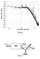
- The generation of in band spurious tones [4] is clearly visible in
FIG. 6 , at frequencies of about 106 Hz and 2·106 Hz. The amplitude of these tones is reduced by 30dB in the reported figure compared to the real value, due to the use of a 1kHz resolution bandwidth for the measurement [4]. - The main drawback of these digital frequency synthesizers compared to the corresponding analog devices is that they suffer of relatively large in-band output spurious tones, which appear near the carrier at frequency offsets that are related to the periodicity in the TDC output pattern, caused by TDC finite resolution. This phenomenon is further worsened by analog mismatches within the TDC.
- A method of improving noise characteristics of an all-digital phase locked loop has been devised.
- The applicants found that in-band spurious tones that corrupt the feedback word generated by an all-digital phase locked loop may be canceled by corrupting with a dither signal the digital word generated by the time-to-digital converter, or the reference clock input to the TDC Fref or the oscillating signal Fout input to the TDC. The novel technique is effective whether the digital word represents the ratio between the reference clock Fref and the oscillating signal Fout, or the DCO output phase.
- This may be done for example by delaying the reference clock Fref or the oscillating signal Fout by a time determined in function of the level of the dither signal.
- According to an embodiment, this may be done by adding a dither signal to the digital word generated by the time-to-digital converter.
- As an option, a second dither signal generated as an inverted and amplified replica of the first dither signal may be added to the digital word generated by the time-to-digital converter, in order to compensate noise introduced by delaying the reference clock or the oscillating signal by a time determined in function of the level of the first dither signal.
- According to an embodiment, variations of the digital word are measured in function of variations of the delay time in respect to a reference delay time and a look-up table is filled with the measured variations and the corresponding variations of the delay time. By generating the dither signal as a pseudo-random signal, in-band noise is minimized by adjusting the amplification gain in order to compensate variations of the digital word due to variations of the delay time according to the values stored in the look-up table.
- A method of generating a digital feedback word of an ADPLL and a relative feedback circuit for an ADPLL and a relative ADPLL are also disclosed.
- The invention is defined in the annexed claims.
-
-
FIG. 1 : Example of a high performance fractional ADPLL block diagram without feedback divider. -
FIG. 2 : Another example of a fractional ADPLL. -
FIG. 3 : Complete TDC block diagram. -
FIG. 4 : TDC counting operation (Fractional Count result is highlighted in gray). -
FIG. 5 : Fractional ADPLL operation with FCW=120.2. (a) Integer counter alone; (b) Integer counter and infinite resolution fractional counter; (c) Integer counter and 4-level fractional counter. -
FIG. 6 : output spectrum of an ADPLL disclosed in [4]. -
FIG. 7 : CF[n] dither by insertion of an analog delay element before the TDC on the reference path. -
FIG. 8 : (a) Small dither does not counteract TDC nonlinearity; (b) large dither forces a large deviation of the TDC output from the value affected by non linearity. -
FIG. 9 : Compensation of the voluntarily injected dither. -
FIG. 10 : Initial estimation phase: single delay value alternated with the "reference delay" value for many samples to achieve a precise measurement of the difference in delay. -
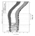
FIG. 11 : White vs shaped dither effect on an ideal ADPLL phase noise spectrum. -
FIG. 12 : Small vs large dither effect on a typical ADPLL phase noise spectrum. -
FIG. 13 : Uniform compensation effect on a typical ADPLL phase noise spectrum. -
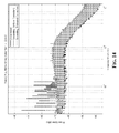
FIG. 14 : Estimated compensation effect on a typical ADPLL phase noise spectrum. - A first embodiment aimed to cancel the spurious tones introduced at the output due to the finite resolution of the TDC (quantization) is depicted in
FIG. 5 . In this figure, the signal (a) is obtained with an integer counter alone, the signals (b) with an integer counter and an infinite resolution fractional counter, the signals (c) with an integer counter and a 4-level fractional counter. As may be observed, although the TDC has perfectly linear quantization steps, the finite resolution causes the ε[n] signal to have periodic information, that produces spurs at the synthesizer output. - To cancel these tones, according to a first embodiment the output CF[n] is corrupted by a dither signal such that the quantization error becomes randomized. This can be achieved for example by injecting a dither signal with a small amplitude, for example of about one quantization step of the TDC, either as a variable analog delay element immediately before the TDC on the reference path (
FIG. 6 ) or on the DCO path (Fout inFIG. 6 ), or in a second embodiment (not depicted) as a digital signal added to the TDC output Fout/Fref. - Because the signal path from the injected dither signal to the ADPLL output is low-pass, a shaped dither signal is preferably used to avoid a negative impact to the in-band noise. More particularly, a dither signal whose energy increases with frequency is preferably used, such that the in-band contribution is negligible and the low-pass nature of the loop counteracts the higher noise power out of band. Independently on whether the spectral density of the dither signal is white or highpass shaped, a multi-level dither is more effective than a two-level dither.
- A multi-level dither can be done by using a programmable delay element (or any alternative means for phase programmability) with a fine delay granularity. Mismatches in the extra delay element itself do not negatively affect performances.
- The novel technique of this disclosure removes spurs due to temporal quantization inherent in the TDC, while requiring minimal hardware modifications to a TDC-based ADPLL. By placing a variable delay element before the TDC and providing a properly shaped dither signal, as shown in
FIG. 7 , minimal impact to in-band noise performance is achieved. - An injected dither signal of relatively small amplitude is sufficient to break the periodicity of the quantization error signal on ε[n], however such a dither signal is insufficient to counteract the effects of TDC nonlinearity, which is another major cause of spur increase in TDC based ADPLLs. In order to counteract TDC nonlinearity (as exemplified in
FIG. 8 ), a dither signal of sufficient magnitude must be introduced. - In doing so, a reduction of spur power is traded for an increase of the in-band noise floor, which is no longer dominated by TDC output noise, as it was in the case of the previous embodiment.
- In a hardware implementation of the algorithm, instead of a truly random dither signal, a pseudorandom dither signal generated by a LFSR (Linear Feedback Shift Register) of sufficient length with respect to fractional periodicity is preferably used.
- The novel technique of this disclosure increases the amplitude of the dither signal and uses a multi-level dither sequence and so allows reduction of spurs due to non-linearity of the TDC to below the in-band noise floor, trading for an increase of the in-band noise power.
- Another improvement consists in compensating the undesired effect of the voluntarily injected dither, that is the effect of increasing the in-band noise floor. In fact, if the input dither is a pseudorandom sequence, it is always possible to predict the resulting injected phase error and thus to compensate it, as shown in
FIG. 9 . - With this embodiment it is possible to choose an arbitrary dither signal for effectively reducing the spur increase due to TDC nonlinearities. The gain α relating the analog delays to the digital compensation signal is a high-resolution word, and thus can be precisely controlled.
- This is an additional advantage over an analog calibration solution, wherein the adjustable gain to be calibrated cannot be determined very precisely because of analog mismatches. Even a rough estimation of the value of the gain α is enough to obtain significant compensation effectiveness.
- According to an embodiment, digitally cancelling the introduced dither using a digital feed-forward path achieves the same reduction of spurs due to both quantization and non-linearity without penalizing significantly the in-band noise power.
- According to another embodiment, a technique for an accurate estimation of the gain α used for compensation is used to make the in-band noise floor equal to that of an undithered ADPLL. According to this method, during an initial digital estimation phase, a delay value of the additional variable delay element is chosen to be the "reference delay". Then, a different delay value to be calibrated against the "reference delay" is alternated for many samples with the "reference delay", as shown in
FIG. 10 , for the simplified case of a short periodicity channel with a large number of TDC quantization levels. - At the end of this sample collection phase, each sample is subtracted from the previous one for measuring the relative time difference between the delays in terms of TDC output values TDCOUT. The absolute values of the results are averaged, obtaining an accurate measurement of the relative time difference between the delays for various TDC output values.
- By taking a plurality of samples and choosing an appropriate channel for the calibration phase, it is possible to ensure that the full range of the TDC is swept and thus all nonlinearities are substantially averaged out. By computing the digital value corresponding to each analog delay level of the additional variable delay element instead of using a single constant α for various delay levels, a look-up table is filled in and is used for canceling effects of non-linearities in the additional delay element itself. This method produces an accurate matching between the analog delay element and the digital feed-forward path.
- This preferred technique, based on a digital estimation preferably executed at the start-up of the proposed ADPLL, relaxes analog precision requirements of the delay element of the embodiments disclosed hereinbefore.
- The most preferred embodiment of the proposed method is in practice a self-calibrating spur reduction method for ADPLLs with no impact to the in-band noise floor.
- Let us consider an exemplary test case of an ADPLL used to synthesize fractional channels around 3GHz, starting from a 25MHz reference frequency, with closed loop bandwidth of about 1MHz, using a 25 bit FCW (7 bits for the integer part, 18 bits for the fractional part). A 42 levels fractional TDC is used (i.e. with a resolution of 333ps/42=8ps). As an example, a 3kHz fractionality channel (FCW=120+25/218) is selected.
- To show the effectiveness of the first proposed embodiment (
FIG. 6 ), let us consider the case of an ideal ADPLL. Only the TDC quantization effect is kept into account inside the ADPLL loop. The applied dither signal has a dynamic range equal to ±1 LSB of the fractional TDC (± 8ps) and a step of 1ps (16 levels). The effect of white and 1st order shaped dither on the ADPLL phase noise around the carrier is compared inFIG. 11 . - To show the effectiveness of the second proposed embodiment, consider the case of a real ADPLL. Also the TDC mismatch effect is kept into account inside the ADPLL model. A white dither is applied. The effects of a dither dynamic range equal to ±1 LSB of the fractional TDC (± 8ps) and of ±8 LSB of the fractional TDC (± 64ps), with a step of 1ps (16 vs 64 levels), are compared in
FIG. 12 . - To show the effectiveness of the third proposed embodiment (
FIG. 9 ), consider the case of a real ADPLL. Also the TDC mismatch effect is kept into account inside the ADPLL loop. A white dither is applied, with a dither dynamic range equal to ±8 LSB of the fractional TDC (± 64ps) and a nominal step of 8ps (16 levels). Mismatches between the dither levels are kept into account. The effects of a compensation based on the nominal step value and without the compensation are compared inFIG. 13 . - To show the effectiveness of the most preferred embodiment, consider the case of a real ADPLL. Also the TDC mismatch effect is kept into account inside the ADPLL loop. A white dither is applied, with a dither dynamic range equal to ±8 LSB of the fractional TDC (± 64ps) and a nominal step of 8ps (16 levels). Mismatches between the dither levels are kept into account. The effects of a compensation based on the nominal step value and with the estimated value using the proposed digital estimation algorithm are compared in
FIG. 14 . -
- [1] A. V. Rylyakov, J. A. Tierno, D. Z. Turker, J.-O. Plouchart, H. A. Ainspan, D. Friedman, "A modular all-digital PLL architecture enabling both 1 to 2 GHz and 24-to-32 GHz operation in 65nm CMOS", 2008 IEEE International Solid-State Circuits Conference, Session 28, Non-volatile memory & digital clocking, 28.6, pages 516-517.
- [2] R. B. Staszewski, D. Leipold, C.-M. Hung, P. T. Balsara, "TDC-based frequency synthesizer for wireless applications", 2004 IEEE Radio Frequency Integrated Symposium, pages 215-218.
- [3] R. B. Staszewski, J. L. Wallberg, S. Rezeq, C.-M. Hung, O. E. Eliezer, S. K. Vemulapalli, C. Fernando, K. Maggio, R. Staszewski, N. Barton, M.-C. Lee, P. Cruise, M. Entezari, K. Muhammad, D. Leipold, "All-digital PLL and transmitter for mobile phones", IEEE Journal of Solid-State Circuits, Vol. 40, No. 12, December 2005, pages 2469-2482.
- [4] R. Tonietto, E. Zuffetti, R. Castello, I. Bietti, "A 3MHz bandwidth low noise RF all digital PLL with 12ps resolution time to digital converter", Proceedings of the ESSCIRC 2006, September 18 - 22, 2006, pages 150-153.
- [5] C. Weltin-Wu, E. Temporiti, D. Baldi, F. Svelto, "A 3GHz fractional-N all-digital PLL with precise time-to-digital converter calibration and mismatch correction", 2008 IEEE International Solid-State Circuits Conference, Session 19, PLLs & Oscillators, 19.3, pages 344-345.
- [6] I. L. Syllaios, R. B. staszewski, P. T. Balsara, "Time-domain modeling of an RF All-Digital PLL", IEEE Trans. Circuits Syst. II, Exp. Briefs, vol. 55, n°6 pp. 601-605, June 2008.
Claims (11)
- A method of improving noise characteristics of an all-digital phase locked loop generating a feedback word representing a continuous-time oscillating signal (Fout), including a time-to-digital converter input with said continuous-time oscillating signal (Fout) and a reference signal (FrefTDC) function of a reference clock (Fref), said time-to-digital converter generating a digital word (TDCOUT) representing either the ratio between said oscillating signal (Fout) and said reference signal (FrefTDC) or the DCO output phase, said feedback word being a function of said digital word (TDCOUT), characterized in that the method comprises
corrupting with a dither signal at least one among said reference clock (Fref), said digital word (TDCOUT) and said oscillating signal (Fout). - The method of claim 1, comprising the step of either generating said reference signal (FrefTDC) by delaying said reference clock (Fref), or inputting to said time-to-digital converter a replica of said oscillating signal (Fout) delayed by a time determined in function of the level of said dither signal.
- The method of claim 1, comprising the step of generating said feedback word by adding said dither signal to said digital word (TDCOUT).
- The method of claim 2, wherein said dither signal is a pseudo-random sequence, the method further comprising the step of generating said feedback word by adding said digital word (TDCOUT) to a second dither signal generated as an inverted and amplified replica of said first dither signal by an amplification gain.
- The method of one of claims from 1 to 4, wherein said dither signal is of a multi-level type and/or the spectrum of frequency amplitudes of said dither signal is relatively small in a certain frequency band and increases with frequency out of said pass-band.
- The method of claim 4, further comprising the steps of:measuring variations of said digital word (TDCOUT) in function of variations of said delay time in respect to a reference delay time and filling a look-up table with the measured variations and the corresponding variations of said delay time;generating said first dither signal as a pseudo-random signal;minimizing in-band noise by adjusting said amplification gain in order to compensate variations of said digital word (TDCOUT) due to variations of said delay time according to the values stored in said look-up table.
- A method of generating a digital feedback word of an all-digital phase locked loop (ADPLL) generating a feedback word representing a continuous-time oscillating signal (Fout) through a time-to-digital converter input with said continuous-time oscillating signal (Fout) and a reference signal (FrefTDC) function of a reference clock (Fref), by generating with said time-to-digital converter a digital word (TDCOUT) representing either the ratio between said oscillating signal (Fout) and said reference signal (FrefTDC) or their mutual outphasing, said feedback word being a function of said digital word (TDCOUT), characterized in that the method comprises the step of improving noise characteristics of the all-digital phase locked loop by executing the method of one of claims from 1 to 6.
- A feedback circuit for an all-digital phase locked loop, generating a feedback word representing a continuous-time oscillating signal (Fout) and including a time-to-digital converter input with said continuous-time oscillating signal (Fout) and a reference signal (FrefTDC) function of a reference clock (Fref), said time-to-digital converter being adapted to generate a digital word (TDCOUT) representing either the ratio between said oscillating signal (Fout) and said reference signal (FrefTDC) or their mutual outphasing, said feedback word being a function of said digital word (TDCOUT), characterized in that said feedback circuit further comprises:a delay circuit input with either said reference clock (Fref) or said oscillating signal (Fout), being controlled by a dither signal and being either adapted to generate said reference signal (FrefTDC) as a replica of said reference clock (Fref) delayed by a time determined by the level of said dither signal, or being adapted to input the time-to-digital converter with a replica of said oscillating signal (Fout) delayed by a time determined by the level of said dither signal, in the latter case said reference signal (FrefTDC) being a replica of said reference clock (Fref).
- The feedback circuit of claim 8, further comprising:an inverting amplifier input with said dither signal and adapted to generate a second dither signal as an amplified replica of said first dither signal;an adder adapted to generate said feedback word as the sum of said digital word (TDCOUT) with said second dither signal.
- A feedback circuit for an all-digital phase locked loop, generating a feedback word representing a continuous-time oscillating signal (Fout) and including a time-to-digital converter input with said continuous-time oscillating signal (Fout) and a reference signal (FrefTDC) function of a reference clock (Fref, said time-to-digital converter being adapted to generate a digital word (TDCOUT) representing either the ratio between said oscillating signal (Fout) and said reference signal (FrefTDC) or their mutual outphasing, said feedback word being a function of said digital word (TDCOUT), characterized in that said feedback circuit further comprises:an adder adapted to generate said feedback word as the sum of said digital word (TDCOUT) with said dither signal.
- An all-digital phase locked loop, comprising a feedback circuit as defined in one of claims from 8 to 10.
Applications Claiming Priority (1)
| Application Number | Priority Date | Filing Date | Title |
|---|---|---|---|
| ITVA20080060 | 2008-12-04 |
Publications (2)
| Publication Number | Publication Date |
|---|---|
| EP2194646A1 true EP2194646A1 (en) | 2010-06-09 |
| EP2194646B1 EP2194646B1 (en) | 2013-01-02 |
Family
ID=40903734
Family Applications (1)
| Application Number | Title | Priority Date | Filing Date |
|---|---|---|---|
| EP09177501A Active EP2194646B1 (en) | 2008-12-04 | 2009-11-30 | Method of improving noise characteristics of an ADPLL and a relative ADPLL |
Country Status (2)
| Country | Link |
|---|---|
| US (1) | US7940099B2 (en) |
| EP (1) | EP2194646B1 (en) |
Cited By (1)
| Publication number | Priority date | Publication date | Assignee | Title |
|---|---|---|---|---|
| EP3249817A1 (en) | 2016-05-25 | 2017-11-29 | IMEC vzw | Dtc-based pll and method for operating the dtc-based pll |
Families Citing this family (21)
| Publication number | Priority date | Publication date | Assignee | Title |
|---|---|---|---|---|
| JP2010034618A (en) * | 2008-07-24 | 2010-02-12 | Sony Corp | Pll circuit, radio terminal device, and control method of pll circuit |
| US8134393B1 (en) * | 2010-09-29 | 2012-03-13 | Motorola Solutions, Inc. | Method and apparatus for correcting phase offset errors in a communication device |
| US8548111B2 (en) | 2010-09-30 | 2013-10-01 | ST-Ericsson-SA | Sampler circuit |
| US8395428B2 (en) | 2010-09-30 | 2013-03-12 | St-Ericsson Sa | Reference clock sampling digital PLL |
| US8749280B2 (en) * | 2011-10-17 | 2014-06-10 | Mediatek Inc. | Frequency synthesizer and associated method |
| US8669890B2 (en) * | 2012-01-20 | 2014-03-11 | Mediatek Inc. | Method and apparatus of estimating/calibrating TDC mismatch |
| EP2796945A1 (en) * | 2013-04-24 | 2014-10-29 | Asahi Kasei Microdevices Corporation | Time-to-digital conversion with analog dithering |
| WO2016063700A1 (en) * | 2014-10-22 | 2016-04-28 | ソニー株式会社 | Phase synchronization circuit and frequency synthesizer |
| EP3119000B1 (en) * | 2015-07-17 | 2018-03-28 | Stichting IMEC Nederland | All digital phase locked loop |
| EP3190704B1 (en) * | 2016-01-06 | 2018-08-01 | Nxp B.V. | Digital phase locked loops |
| US10715157B2 (en) | 2016-03-31 | 2020-07-14 | Apple Inc. | Methods and mobile communication devices for performing spur relocation for phase-locked loops |
| JP6572251B2 (en) | 2017-03-17 | 2019-09-04 | 株式会社東芝 | Time measuring circuit and distance measuring device |
| WO2019017864A1 (en) * | 2017-07-17 | 2019-01-24 | Intel IP Corporation | A method and a system for calibrating a phase nonlinearity of a digital-to-time converter |
| US10516401B2 (en) * | 2018-03-09 | 2019-12-24 | Texas Instruments Incorporated | Wobble reduction in an integer mode digital phase locked loop |
| JP2019161442A (en) | 2018-03-13 | 2019-09-19 | 株式会社東芝 | TDC circuit and PLL circuit |
| JP2021027496A (en) * | 2019-08-07 | 2021-02-22 | セイコーエプソン株式会社 | Circuit device, physical amount measurement device, electronic apparatus, and movable body |
| CN110784212B (en) * | 2019-11-18 | 2020-06-30 | 华南理工大学 | A frequency locking method and circuit of a phase-locked loop |
| JP7619622B2 (en) | 2021-05-17 | 2025-01-22 | 北陽電機株式会社 | TDC device, distance measuring device and correction method |
| JP7619623B2 (en) | 2021-05-17 | 2025-01-22 | 北陽電機株式会社 | TDC device, ranging device and ranging method |
| US11658666B1 (en) * | 2022-03-30 | 2023-05-23 | Nxp B.V. | Fractional-N ADPLL with reference dithering |
| CN115421367B (en) * | 2022-08-10 | 2024-02-27 | 麦斯塔微电子(深圳)有限公司 | Calibration methods and systems |
Citations (2)
| Publication number | Priority date | Publication date | Assignee | Title |
|---|---|---|---|---|
| US20060103566A1 (en) * | 2004-11-18 | 2006-05-18 | Texas Instruments Incorporated | Circuit for high-resolution phase detection in a digital RF processor |
| EP1956714A1 (en) * | 2007-02-08 | 2008-08-13 | Stmicroelectronics SA | Method for adding random noise in a time-to-digital converter circuit and circuits for implementing the method |
Family Cites Families (6)
| Publication number | Priority date | Publication date | Assignee | Title |
|---|---|---|---|---|
| US7498890B2 (en) * | 2005-10-19 | 2009-03-03 | Texas Instruments Incorporated | Continuous reversible gear shifting mechanism |
| US7714665B2 (en) * | 2006-02-16 | 2010-05-11 | Texas Instruments Incorporated | Harmonic characterization and correction of device mismatch |
| JP2008060895A (en) * | 2006-08-31 | 2008-03-13 | Nec Electronics Corp | Phase-locked circuit |
| US8045670B2 (en) * | 2007-06-22 | 2011-10-25 | Texas Instruments Incorporated | Interpolative all-digital phase locked loop |
| US8433025B2 (en) * | 2008-01-04 | 2013-04-30 | Qualcomm Incorporated | Digital phase-locked loop with gated time-to-digital converter |
| US20100074387A1 (en) * | 2008-09-24 | 2010-03-25 | Infineon Technologies Ag | Frequency to Phase Converter with Uniform Sampling for all Digital Phase Locked Loops |
-
2009
- 2009-11-30 EP EP09177501A patent/EP2194646B1/en active Active
- 2009-12-03 US US12/630,585 patent/US7940099B2/en active Active
Patent Citations (2)
| Publication number | Priority date | Publication date | Assignee | Title |
|---|---|---|---|---|
| US20060103566A1 (en) * | 2004-11-18 | 2006-05-18 | Texas Instruments Incorporated | Circuit for high-resolution phase detection in a digital RF processor |
| EP1956714A1 (en) * | 2007-02-08 | 2008-08-13 | Stmicroelectronics SA | Method for adding random noise in a time-to-digital converter circuit and circuits for implementing the method |
Non-Patent Citations (6)
| Title |
|---|
| 1. L. SYLLAIOS; R. B. STASZEWSKI; P. T. BALSARA: "Time-domain modeling of an RF All-Digital PLL", IEEE TRANS. CIRCUITS SYST. II, EXP. BRIEFS, vol. 55, no. 6, June 2008 (2008-06-01), pages 601 - 605 |
| A. V. RYLYAKOV ET AL.: "A modular all-digital PLL architecture enabling both 1 to 2 GHz and 24-to-32 GHz operation in 65nm CMOS", 2008 IEEE INTERNATIONAL SOLID-STATE CIRCUITS CONFERENCE, pages 516 - 517 |
| C. WELTIN-WU ET AL.: "A 3GHz fractional-N all-digital PLL with precise time-to-digital converter calibration and mismatch correction", IEEE INTERNATIONAL SOLID-STATE CIRCUITS CONFERENCE, vol. 19.3, 2008, pages 344 - 345 |
| R. B. STASZEWSKI ET AL.: "All-digital PLL and transmitter for mobile phones", IEEE JOURNAL OF SOLID-STATE CIRCUITS, vol. 40, no. 12, December 2005 (2005-12-01), pages 2469 - 2482 |
| R. B. STASZEWSKI ET AL.: "TDC-based frequency synthesizer for wireless applications", 2004 IEEE RADIO FREQUENCY INTEGRATED SYMPOSIUM, pages 215 - 218 |
| R. TONIETTO ET AL.: "A 3MHz bandwidth low noise RF all digital PLL with 12ps resolution time to digital converter", PROCEEDINGS OF THE ESSCIRC, vol. 22, 18 September 2006 (2006-09-18), pages 150 - 153 |
Cited By (2)
| Publication number | Priority date | Publication date | Assignee | Title |
|---|---|---|---|---|
| EP3249817A1 (en) | 2016-05-25 | 2017-11-29 | IMEC vzw | Dtc-based pll and method for operating the dtc-based pll |
| US10200047B2 (en) | 2016-05-25 | 2019-02-05 | Imec Vzw | DTC-based PLL and method for operating the DTC-based PLL |
Also Published As
| Publication number | Publication date |
|---|---|
| US20100141316A1 (en) | 2010-06-10 |
| EP2194646B1 (en) | 2013-01-02 |
| US7940099B2 (en) | 2011-05-10 |
Similar Documents
| Publication | Publication Date | Title |
|---|---|---|
| EP2194646B1 (en) | Method of improving noise characteristics of an ADPLL and a relative ADPLL | |
| CN113169738B (en) | Adaptive Nonlinear Identification and Compensation Using Orthogonal Functions in Mixed-Signal Circuits | |
| De Muer et al. | CMOS fractional-N synthesizers: design for high spectral purity and monolithic integration | |
| Levantino et al. | An adaptive pre-distortion technique to mitigate the DTC nonlinearity in digital PLLs | |
| US9762250B2 (en) | Cancellation of spurious tones within a phase-locked loop with a time-to-digital converter | |
| US7365607B2 (en) | Low-power, low-jitter, fractional-N all-digital phase-locked loop (PLL) | |
| Pamarti et al. | A wideband 2.4-GHz delta-sigma fractional-NPLL with 1-Mb/s in-loop modulation | |
| US9705521B1 (en) | Noise shaping signed digital-to-analog converter | |
| US10680624B2 (en) | Phase-locked loop with filtered quantization noise | |
| US8198929B2 (en) | Dynamic element matching for time-to-digital converters | |
| Venerus et al. | A TDC-free mostly-digital FDC-PLL frequency synthesizer with a 2.8-3.5 GHz DCO | |
| Su et al. | Fractional-$ N $ Phase-Locked-Loop-Based Frequency Synthesis: A Tutorial | |
| WO2010032184A2 (en) | Signal processing using timing comparison | |
| US7271666B1 (en) | Method and apparatus for canceling jitter in a fractional-N phase-lock loop (PLL) | |
| Kennedy et al. | Nonlinearity-induced spurs in fractional-N frequency synthesizers | |
| Rhee et al. | Fractional-N frequency synthesis: overview and practical aspects with FIR-embedded design | |
| US20250167797A1 (en) | Dtc linearization via mismatch-noise cancellation for digital fractional-n plls | |
| Moreira et al. | Distributed DDS in a white rabbit network: An IEEE 1588 application | |
| Chen | Trends and new opportunities in digital phase-locked loop design: Design principles, key overheads, and new opportunities in this emerging architecture | |
| Wang et al. | Linearized analysis and quantization error minimization for mid-rise TDCs: A tutorial | |
| Temporiti et al. | Insights into wideband fractional all-digital PLLs for RF applications | |
| Pamarti | Digital techniques for integrated frequency synthesizers: A tutorial | |
| US20250247099A1 (en) | Suppressing spurious tones resulting from the requantization of the accumulated quantization error when performing fractional frequency division | |
| Borkowski | Digital Δ-Σ Modulation: variable modulus and tonal behaviour in a fixed-point digital environment | |
| Reddy | Noise shaping with sigma delta modulators in fractional-N synthesizers |
Legal Events
| Date | Code | Title | Description |
|---|---|---|---|
| PUAI | Public reference made under article 153(3) epc to a published international application that has entered the european phase |
Free format text: ORIGINAL CODE: 0009012 |
|
| AK | Designated contracting states |
Kind code of ref document: A1 Designated state(s): AT BE BG CH CY CZ DE DK EE ES FI FR GB GR HR HU IE IS IT LI LT LU LV MC MK MT NL NO PL PT RO SE SI SK SM TR |
|
| AX | Request for extension of the european patent |
Extension state: AL BA RS |
|
| 17P | Request for examination filed |
Effective date: 20101126 |
|
| 17Q | First examination report despatched |
Effective date: 20110112 |
|
| RAP1 | Party data changed (applicant data changed or rights of an application transferred) |
Owner name: STMICROELECTRONICS SRL |
|
| GRAP | Despatch of communication of intention to grant a patent |
Free format text: ORIGINAL CODE: EPIDOSNIGR1 |
|
| GRAS | Grant fee paid |
Free format text: ORIGINAL CODE: EPIDOSNIGR3 |
|
| GRAA | (expected) grant |
Free format text: ORIGINAL CODE: 0009210 |
|
| AK | Designated contracting states |
Kind code of ref document: B1 Designated state(s): AT BE BG CH CY CZ DE DK EE ES FI FR GB GR HR HU IE IS IT LI LT LU LV MC MK MT NL NO PL PT RO SE SI SK SM TR |
|
| REG | Reference to a national code |
Ref country code: GB Ref legal event code: FG4D |
|
| REG | Reference to a national code |
Ref country code: CH Ref legal event code: EP Ref country code: AT Ref legal event code: REF Ref document number: 592084 Country of ref document: AT Kind code of ref document: T Effective date: 20130115 |
|
| REG | Reference to a national code |
Ref country code: IE Ref legal event code: FG4D |
|
| REG | Reference to a national code |
Ref country code: DE Ref legal event code: R096 Ref document number: 602009012410 Country of ref document: DE Effective date: 20130228 |
|
| REG | Reference to a national code |
Ref country code: AT Ref legal event code: MK05 Ref document number: 592084 Country of ref document: AT Kind code of ref document: T Effective date: 20130102 |
|
| REG | Reference to a national code |
Ref country code: NL Ref legal event code: VDEP Effective date: 20130102 |
|
| PG25 | Lapsed in a contracting state [announced via postgrant information from national office to epo] |
Ref country code: SI Free format text: LAPSE BECAUSE OF FAILURE TO SUBMIT A TRANSLATION OF THE DESCRIPTION OR TO PAY THE FEE WITHIN THE PRESCRIBED TIME-LIMIT Effective date: 20130102 |
|
| REG | Reference to a national code |
Ref country code: LT Ref legal event code: MG4D |
|
| PG25 | Lapsed in a contracting state [announced via postgrant information from national office to epo] |
Ref country code: BG Free format text: LAPSE BECAUSE OF FAILURE TO SUBMIT A TRANSLATION OF THE DESCRIPTION OR TO PAY THE FEE WITHIN THE PRESCRIBED TIME-LIMIT Effective date: 20130402 Ref country code: SE Free format text: LAPSE BECAUSE OF FAILURE TO SUBMIT A TRANSLATION OF THE DESCRIPTION OR TO PAY THE FEE WITHIN THE PRESCRIBED TIME-LIMIT Effective date: 20130102 Ref country code: BE Free format text: LAPSE BECAUSE OF FAILURE TO SUBMIT A TRANSLATION OF THE DESCRIPTION OR TO PAY THE FEE WITHIN THE PRESCRIBED TIME-LIMIT Effective date: 20130102 Ref country code: ES Free format text: LAPSE BECAUSE OF FAILURE TO SUBMIT A TRANSLATION OF THE DESCRIPTION OR TO PAY THE FEE WITHIN THE PRESCRIBED TIME-LIMIT Effective date: 20130413 Ref country code: CZ Free format text: LAPSE BECAUSE OF FAILURE TO SUBMIT A TRANSLATION OF THE DESCRIPTION OR TO PAY THE FEE WITHIN THE PRESCRIBED TIME-LIMIT Effective date: 20130102 Ref country code: AT Free format text: LAPSE BECAUSE OF FAILURE TO SUBMIT A TRANSLATION OF THE DESCRIPTION OR TO PAY THE FEE WITHIN THE PRESCRIBED TIME-LIMIT Effective date: 20130102 Ref country code: IS Free format text: LAPSE BECAUSE OF FAILURE TO SUBMIT A TRANSLATION OF THE DESCRIPTION OR TO PAY THE FEE WITHIN THE PRESCRIBED TIME-LIMIT Effective date: 20130502 Ref country code: LT Free format text: LAPSE BECAUSE OF FAILURE TO SUBMIT A TRANSLATION OF THE DESCRIPTION OR TO PAY THE FEE WITHIN THE PRESCRIBED TIME-LIMIT Effective date: 20130102 Ref country code: NO Free format text: LAPSE BECAUSE OF FAILURE TO SUBMIT A TRANSLATION OF THE DESCRIPTION OR TO PAY THE FEE WITHIN THE PRESCRIBED TIME-LIMIT Effective date: 20130402 |
|
| PG25 | Lapsed in a contracting state [announced via postgrant information from national office to epo] |
Ref country code: NL Free format text: LAPSE BECAUSE OF FAILURE TO SUBMIT A TRANSLATION OF THE DESCRIPTION OR TO PAY THE FEE WITHIN THE PRESCRIBED TIME-LIMIT Effective date: 20130102 Ref country code: FI Free format text: LAPSE BECAUSE OF FAILURE TO SUBMIT A TRANSLATION OF THE DESCRIPTION OR TO PAY THE FEE WITHIN THE PRESCRIBED TIME-LIMIT Effective date: 20130102 Ref country code: GR Free format text: LAPSE BECAUSE OF FAILURE TO SUBMIT A TRANSLATION OF THE DESCRIPTION OR TO PAY THE FEE WITHIN THE PRESCRIBED TIME-LIMIT Effective date: 20130403 Ref country code: PT Free format text: LAPSE BECAUSE OF FAILURE TO SUBMIT A TRANSLATION OF THE DESCRIPTION OR TO PAY THE FEE WITHIN THE PRESCRIBED TIME-LIMIT Effective date: 20130502 Ref country code: LV Free format text: LAPSE BECAUSE OF FAILURE TO SUBMIT A TRANSLATION OF THE DESCRIPTION OR TO PAY THE FEE WITHIN THE PRESCRIBED TIME-LIMIT Effective date: 20130102 Ref country code: PL Free format text: LAPSE BECAUSE OF FAILURE TO SUBMIT A TRANSLATION OF THE DESCRIPTION OR TO PAY THE FEE WITHIN THE PRESCRIBED TIME-LIMIT Effective date: 20130102 |
|
| PG25 | Lapsed in a contracting state [announced via postgrant information from national office to epo] |
Ref country code: HR Free format text: LAPSE BECAUSE OF FAILURE TO SUBMIT A TRANSLATION OF THE DESCRIPTION OR TO PAY THE FEE WITHIN THE PRESCRIBED TIME-LIMIT Effective date: 20130102 |
|
| PG25 | Lapsed in a contracting state [announced via postgrant information from national office to epo] |
Ref country code: SK Free format text: LAPSE BECAUSE OF FAILURE TO SUBMIT A TRANSLATION OF THE DESCRIPTION OR TO PAY THE FEE WITHIN THE PRESCRIBED TIME-LIMIT Effective date: 20130102 Ref country code: EE Free format text: LAPSE BECAUSE OF FAILURE TO SUBMIT A TRANSLATION OF THE DESCRIPTION OR TO PAY THE FEE WITHIN THE PRESCRIBED TIME-LIMIT Effective date: 20130102 Ref country code: RO Free format text: LAPSE BECAUSE OF FAILURE TO SUBMIT A TRANSLATION OF THE DESCRIPTION OR TO PAY THE FEE WITHIN THE PRESCRIBED TIME-LIMIT Effective date: 20130102 Ref country code: DK Free format text: LAPSE BECAUSE OF FAILURE TO SUBMIT A TRANSLATION OF THE DESCRIPTION OR TO PAY THE FEE WITHIN THE PRESCRIBED TIME-LIMIT Effective date: 20130102 |
|
| PLBE | No opposition filed within time limit |
Free format text: ORIGINAL CODE: 0009261 |
|
| STAA | Information on the status of an ep patent application or granted ep patent |
Free format text: STATUS: NO OPPOSITION FILED WITHIN TIME LIMIT |
|
| PG25 | Lapsed in a contracting state [announced via postgrant information from national office to epo] |
Ref country code: CY Free format text: LAPSE BECAUSE OF FAILURE TO SUBMIT A TRANSLATION OF THE DESCRIPTION OR TO PAY THE FEE WITHIN THE PRESCRIBED TIME-LIMIT Effective date: 20130102 |
|
| 26N | No opposition filed |
Effective date: 20131003 |
|
| REG | Reference to a national code |
Ref country code: DE Ref legal event code: R097 Ref document number: 602009012410 Country of ref document: DE Effective date: 20131003 |
|
| PGFP | Annual fee paid to national office [announced via postgrant information from national office to epo] |
Ref country code: IT Payment date: 20131023 Year of fee payment: 5 |
|
| REG | Reference to a national code |
Ref country code: CH Ref legal event code: PL |
|
| GBPC | Gb: european patent ceased through non-payment of renewal fee |
Effective date: 20131130 |
|
| PG25 | Lapsed in a contracting state [announced via postgrant information from national office to epo] |
Ref country code: LI Free format text: LAPSE BECAUSE OF NON-PAYMENT OF DUE FEES Effective date: 20131130 Ref country code: MC Free format text: LAPSE BECAUSE OF FAILURE TO SUBMIT A TRANSLATION OF THE DESCRIPTION OR TO PAY THE FEE WITHIN THE PRESCRIBED TIME-LIMIT Effective date: 20130102 Ref country code: CH Free format text: LAPSE BECAUSE OF NON-PAYMENT OF DUE FEES Effective date: 20131130 |
|
| REG | Reference to a national code |
Ref country code: FR Ref legal event code: ST Effective date: 20140731 |
|
| REG | Reference to a national code |
Ref country code: IE Ref legal event code: MM4A |
|
| PG25 | Lapsed in a contracting state [announced via postgrant information from national office to epo] |
Ref country code: IE Free format text: LAPSE BECAUSE OF NON-PAYMENT OF DUE FEES Effective date: 20131130 |
|
| PG25 | Lapsed in a contracting state [announced via postgrant information from national office to epo] |
Ref country code: FR Free format text: LAPSE BECAUSE OF NON-PAYMENT OF DUE FEES Effective date: 20131202 Ref country code: GB Free format text: LAPSE BECAUSE OF NON-PAYMENT OF DUE FEES Effective date: 20131130 |
|
| REG | Reference to a national code |
Ref country code: DE Ref legal event code: R082 Ref document number: 602009012410 Country of ref document: DE |
|
| PG25 | Lapsed in a contracting state [announced via postgrant information from national office to epo] |
Ref country code: SM Free format text: LAPSE BECAUSE OF FAILURE TO SUBMIT A TRANSLATION OF THE DESCRIPTION OR TO PAY THE FEE WITHIN THE PRESCRIBED TIME-LIMIT Effective date: 20130102 |
|
| PG25 | Lapsed in a contracting state [announced via postgrant information from national office to epo] |
Ref country code: TR Free format text: LAPSE BECAUSE OF FAILURE TO SUBMIT A TRANSLATION OF THE DESCRIPTION OR TO PAY THE FEE WITHIN THE PRESCRIBED TIME-LIMIT Effective date: 20130102 |
|
| PG25 | Lapsed in a contracting state [announced via postgrant information from national office to epo] |
Ref country code: LU Free format text: LAPSE BECAUSE OF NON-PAYMENT OF DUE FEES Effective date: 20131130 Ref country code: HU Free format text: LAPSE BECAUSE OF FAILURE TO SUBMIT A TRANSLATION OF THE DESCRIPTION OR TO PAY THE FEE WITHIN THE PRESCRIBED TIME-LIMIT; INVALID AB INITIO Effective date: 20091130 Ref country code: MK Free format text: LAPSE BECAUSE OF FAILURE TO SUBMIT A TRANSLATION OF THE DESCRIPTION OR TO PAY THE FEE WITHIN THE PRESCRIBED TIME-LIMIT Effective date: 20130102 |
|
| PG25 | Lapsed in a contracting state [announced via postgrant information from national office to epo] |
Ref country code: MT Free format text: LAPSE BECAUSE OF FAILURE TO SUBMIT A TRANSLATION OF THE DESCRIPTION OR TO PAY THE FEE WITHIN THE PRESCRIBED TIME-LIMIT Effective date: 20130102 |
|
| PG25 | Lapsed in a contracting state [announced via postgrant information from national office to epo] |
Ref country code: IT Free format text: LAPSE BECAUSE OF NON-PAYMENT OF DUE FEES Effective date: 20141130 |
|
| PGFP | Annual fee paid to national office [announced via postgrant information from national office to epo] |
Ref country code: DE Payment date: 20251022 Year of fee payment: 17 |