EP2194055A1 - Bridged pyridoquinazoline or phenanthroline compounds and organic semiconducting material comprising that compound - Google Patents
Bridged pyridoquinazoline or phenanthroline compounds and organic semiconducting material comprising that compound Download PDFInfo
- Publication number
- EP2194055A1 EP2194055A1 EP08020941A EP08020941A EP2194055A1 EP 2194055 A1 EP2194055 A1 EP 2194055A1 EP 08020941 A EP08020941 A EP 08020941A EP 08020941 A EP08020941 A EP 08020941A EP 2194055 A1 EP2194055 A1 EP 2194055A1
- Authority
- EP
- European Patent Office
- Prior art keywords
- organic
- alkyl
- layer
- compound according
- doped
- Prior art date
- Legal status (The legal status is an assumption and is not a legal conclusion. Google has not performed a legal analysis and makes no representation as to the accuracy of the status listed.)
- Granted
Links
- VWXBYBVQAUVFFP-UHFFFAOYSA-N O=C1c2nc(-c3ccccc3)cc(-c3ccccc3)c2CCC1 Chemical compound O=C1c2nc(-c3ccccc3)cc(-c3ccccc3)c2CCC1 VWXBYBVQAUVFFP-UHFFFAOYSA-N 0.000 description 3
- LGDUZIGBIPSHKN-UHFFFAOYSA-N COC1C=C(C=O)C=C1 Chemical compound COC1C=C(C=O)C=C1 LGDUZIGBIPSHKN-UHFFFAOYSA-N 0.000 description 1
- HNXCEGJABTWIMU-NCOOAAOESA-N O=C1c2nc(-c3ccccc3)cc(-c3ccccc3)c2CC/C1=C\c1cc(-c2cc(/C=C(\CCc(c3nc(-c4ccccc4)c4)c4-c4ccccc4)/C3=O)ccc2)ccc1 Chemical compound O=C1c2nc(-c3ccccc3)cc(-c3ccccc3)c2CC/C1=C\c1cc(-c2cc(/C=C(\CCc(c3nc(-c4ccccc4)c4)c4-c4ccccc4)/C3=O)ccc2)ccc1 HNXCEGJABTWIMU-NCOOAAOESA-N 0.000 description 1
- VSRMOSGGNRZBEH-UTKMUYHOSA-N O=C1c2nc(-c3ccccc3)cc(-c3ccccc3)c2CC/C1=C\c1nc(-c2nc(/C=C(\CCc(c(-c3ccccc3)c3)c4nc3-c3ccccc3)/C4=O)ccc2)ccc1 Chemical compound O=C1c2nc(-c3ccccc3)cc(-c3ccccc3)c2CC/C1=C\c1nc(-c2nc(/C=C(\CCc(c(-c3ccccc3)c3)c4nc3-c3ccccc3)/C4=O)ccc2)ccc1 VSRMOSGGNRZBEH-UTKMUYHOSA-N 0.000 description 1
- KRCLRHSEMGXKMY-UHFFFAOYSA-N O=Cc1cccc(-c2cc(C=O)ccc2)c1 Chemical compound O=Cc1cccc(-c2cc(C=O)ccc2)c1 KRCLRHSEMGXKMY-UHFFFAOYSA-N 0.000 description 1
- NHWCJRHPJLHJPL-UHFFFAOYSA-N O=Cc1cccc(-c2nc(C=O)ccc2)n1 Chemical compound O=Cc1cccc(-c2nc(C=O)ccc2)n1 NHWCJRHPJLHJPL-UHFFFAOYSA-N 0.000 description 1
Images

Classifications
-
- C—CHEMISTRY; METALLURGY
- C07—ORGANIC CHEMISTRY
- C07D—HETEROCYCLIC COMPOUNDS
- C07D471/00—Heterocyclic compounds containing nitrogen atoms as the only ring hetero atoms in the condensed system, at least one ring being a six-membered ring with one nitrogen atom, not provided for by groups C07D451/00 - C07D463/00
- C07D471/02—Heterocyclic compounds containing nitrogen atoms as the only ring hetero atoms in the condensed system, at least one ring being a six-membered ring with one nitrogen atom, not provided for by groups C07D451/00 - C07D463/00 in which the condensed system contains two hetero rings
- C07D471/04—Ortho-condensed systems
-
- H—ELECTRICITY
- H10—SEMICONDUCTOR DEVICES; ELECTRIC SOLID-STATE DEVICES NOT OTHERWISE PROVIDED FOR
- H10K—ORGANIC ELECTRIC SOLID-STATE DEVICES
- H10K85/00—Organic materials used in the body or electrodes of devices covered by this subclass
- H10K85/60—Organic compounds having low molecular weight
- H10K85/649—Aromatic compounds comprising a hetero atom
- H10K85/655—Aromatic compounds comprising a hetero atom comprising only sulfur as heteroatom
-
- H—ELECTRICITY
- H10—SEMICONDUCTOR DEVICES; ELECTRIC SOLID-STATE DEVICES NOT OTHERWISE PROVIDED FOR
- H10K—ORGANIC ELECTRIC SOLID-STATE DEVICES
- H10K85/00—Organic materials used in the body or electrodes of devices covered by this subclass
- H10K85/60—Organic compounds having low molecular weight
- H10K85/649—Aromatic compounds comprising a hetero atom
- H10K85/657—Polycyclic condensed heteroaromatic hydrocarbons
- H10K85/6572—Polycyclic condensed heteroaromatic hydrocarbons comprising only nitrogen in the heteroaromatic polycondensed ring system, e.g. phenanthroline or carbazole
-
- H—ELECTRICITY
- H10—SEMICONDUCTOR DEVICES; ELECTRIC SOLID-STATE DEVICES NOT OTHERWISE PROVIDED FOR
- H10K—ORGANIC ELECTRIC SOLID-STATE DEVICES
- H10K30/00—Organic devices sensitive to infrared radiation, light, electromagnetic radiation of shorter wavelength or corpuscular radiation
- H10K30/20—Organic devices sensitive to infrared radiation, light, electromagnetic radiation of shorter wavelength or corpuscular radiation comprising organic-organic junctions, e.g. donor-acceptor junctions
- H10K30/211—Organic devices sensitive to infrared radiation, light, electromagnetic radiation of shorter wavelength or corpuscular radiation comprising organic-organic junctions, e.g. donor-acceptor junctions comprising multiple junctions, e.g. double heterojunctions
-
- H—ELECTRICITY
- H10—SEMICONDUCTOR DEVICES; ELECTRIC SOLID-STATE DEVICES NOT OTHERWISE PROVIDED FOR
- H10K—ORGANIC ELECTRIC SOLID-STATE DEVICES
- H10K30/00—Organic devices sensitive to infrared radiation, light, electromagnetic radiation of shorter wavelength or corpuscular radiation
- H10K30/30—Organic devices sensitive to infrared radiation, light, electromagnetic radiation of shorter wavelength or corpuscular radiation comprising bulk heterojunctions, e.g. interpenetrating networks of donor and acceptor material domains
-
- H—ELECTRICITY
- H10—SEMICONDUCTOR DEVICES; ELECTRIC SOLID-STATE DEVICES NOT OTHERWISE PROVIDED FOR
- H10K—ORGANIC ELECTRIC SOLID-STATE DEVICES
- H10K30/00—Organic devices sensitive to infrared radiation, light, electromagnetic radiation of shorter wavelength or corpuscular radiation
- H10K30/50—Photovoltaic [PV] devices
-
- H—ELECTRICITY
- H10—SEMICONDUCTOR DEVICES; ELECTRIC SOLID-STATE DEVICES NOT OTHERWISE PROVIDED FOR
- H10K—ORGANIC ELECTRIC SOLID-STATE DEVICES
- H10K50/00—Organic light-emitting devices
- H10K50/10—OLEDs or polymer light-emitting diodes [PLED]
- H10K50/14—Carrier transporting layers
-
- H—ELECTRICITY
- H10—SEMICONDUCTOR DEVICES; ELECTRIC SOLID-STATE DEVICES NOT OTHERWISE PROVIDED FOR
- H10K—ORGANIC ELECTRIC SOLID-STATE DEVICES
- H10K50/00—Organic light-emitting devices
- H10K50/10—OLEDs or polymer light-emitting diodes [PLED]
- H10K50/14—Carrier transporting layers
- H10K50/15—Hole transporting layers
- H10K50/155—Hole transporting layers comprising dopants
-
- H—ELECTRICITY
- H10—SEMICONDUCTOR DEVICES; ELECTRIC SOLID-STATE DEVICES NOT OTHERWISE PROVIDED FOR
- H10K—ORGANIC ELECTRIC SOLID-STATE DEVICES
- H10K50/00—Organic light-emitting devices
- H10K50/10—OLEDs or polymer light-emitting diodes [PLED]
- H10K50/14—Carrier transporting layers
- H10K50/16—Electron transporting layers
- H10K50/165—Electron transporting layers comprising dopants
-
- Y—GENERAL TAGGING OF NEW TECHNOLOGICAL DEVELOPMENTS; GENERAL TAGGING OF CROSS-SECTIONAL TECHNOLOGIES SPANNING OVER SEVERAL SECTIONS OF THE IPC; TECHNICAL SUBJECTS COVERED BY FORMER USPC CROSS-REFERENCE ART COLLECTIONS [XRACs] AND DIGESTS
- Y02—TECHNOLOGIES OR APPLICATIONS FOR MITIGATION OR ADAPTATION AGAINST CLIMATE CHANGE
- Y02E—REDUCTION OF GREENHOUSE GAS [GHG] EMISSIONS, RELATED TO ENERGY GENERATION, TRANSMISSION OR DISTRIBUTION
- Y02E10/00—Energy generation through renewable energy sources
- Y02E10/50—Photovoltaic [PV] energy
- Y02E10/549—Organic PV cells
Definitions
- the present invention relates to bridged pyridoquinazoline and phenanthroline compounds and derivatives thereof, and to organic semiconducting materials and devices containing these compounds.
- Organic semiconductors can be used to fabricate simple electronic components e.g. resistors, diodes, field effect transistors, and also optoelectronic components like light emitting devices (e.g. OLED), solar cells, and many others.
- Non-volatile and volatile, re-writable memories can be created using much different physical mechanism, such as molecular bi-stability, ferromagnetic properties (e.g. US2006073658 ), ion transfer and charge wells (e.g. WO08125100 ).
- the industrial and economical significance of the organic semiconductors and their devices is reflected in the increased number of devices using organic semiconducting active layers and the increasing industry focus on the subject.
- Conjugated organic compounds can be small molecules, for instance monomers, oligomers, polymers, copolymers, copolymers of conjugated and non-conjugated blocks, completely or partially cross-linked layers, aggregate structures, or brush like structures.
- Organic electronic semiconductors can be used in organic electronic devices, and in organic-inorganic hybrid devices.
- Typical organic semiconducting compounds may have a gap that is still high enough so that the compounds are optically active.
- Organic field effect transistors are explained, for example, in US7026643 , US2005146262 and US2008230776 .
- the resistance of a semiconductive layer that is contacted by two electrodes (source and drain) can be controlled by the voltage that is applied to the gate.
- the gate is displaced on an insulator that is displaced parallel in contact to the semiconductive layer.
- Various geometries can be used, such as bottom gate (on the substrate), top gate (on the opposite side of the semiconductive layer relative to the substrate) or on both sides.
- Many different arrangements of layers can be used such as bipolar layers, injection layer, insulating layer between electrode and semiconductive layer to lower the off current, etc.
- OTFTs need high mobility materials in their active channel.
- Transparent circuits, such as transparent OTFTs require that the high mobility organic material also comprises a wide electronic band gap; the electric injection of holes and / or electrons must be still provided.
- Solar cells and OLEDs require transparent transport layers, with high conductivity. The transparency is necessary in those opto-electric devices to avoid non desired absorption of the light.
- These so called “window” materials can be used as transport layers, exciton or charge blocking layers.
- the thickness of the layers made with the window materials is used to adjust the micro cavity of the OLEDs and solar cells in such a way that the outcoupled emission of the OLED is a maximum, and in the case of the solar cell, the absorption and respective photocurrent of the device is a maximum.
- the non-optically active layers of all kinds of semiconductor devices can be exchanged for window materials in order to fabricate fully transparent components and circuits (e.g US20060033115 ).
- Electronic devices also need high stability towards temperature, meaning that the intrinsic properties of the amorphous organic semiconducting materials, such as triphenyl amine derivatives, or phenantronine derivatives, must include a high glass transition temperature (Tg) and high temperature stability in the device.
- Tg glass transition temperature
- the conductivity can be, for example, measured by the so-called 2-point or 4-point-method.
- contacts of a conductive material such as gold or indium-tin-oxide
- the thin film to be examined is applied onto the substrate, so that the contacts are covered by the thin film.
- the current is measured. From the geometry of the contacts and the thickness of the sample the resistance and therefore the conductivity of the thin film material can be determined.
- the four point or two point method give the same conductivity values for doped layers since the doped layers grant a good ohmic contact.
- the temperature stability can be also measured with that method in that the (undoped or doped) layer is heated stepwise, and after a waiting period the conductivity is measured.
- the maximum temperature which can be applied to the layer without loosing the desired semiconducting properties, is then the temperature just before the conductivity breaks down.
- a doped layer can be heated on the substrate with two electrodes, as disclosed above, in steps of 1°C, wherein after each step there is a waiting period of 10 seconds. Then the conductivity is measured.
- the conductivity changes with temperature and breaks down abruptly at a particular temperature.
- the temperature stability is therefore the temperature up to which the conductivity does not break down abruptly.
- the measurement is performed in vacuum.
- HOMO highest occupied molecular orbital energy level
- LUMO lowest unoccupied molecular orbital energy level
- IP ionization potentials
- UPS ultraviolet photo spectroscopy
- the IP is related to beginning of the photoemission spectra in the region of the large kinetic energy of the photoelectrons, i.e. the energy of the most weakly bounded electrons.
- a related method to UPS, the inverted photo electron spectroscopy (IPES) can be used to determine the electron affinity (EA) (see e.g. W. Gao et. al, Appl. Phys. Lett. 82, 4815 (2003 ). However, this method is less common.
- Electrochemical measurements in solution are an alternative to the determination of solid state oxidation (Eox) and reduction (Ered) potential.
- the given potentials correspond to the solid-state potentials.
- the HOMO levels of the emitter materials are in the range of 5 eV to 6.5 eV, and the LUMO in the range from 2 to 3 eV.
- Electron transport materials including their respective blockers, have their HOMO in range of 5,5 eV to 6.8 eV and LUMO in the range of 2,3 eV to 3.3 eV, larger (lower laying) LUMO and HOMO levels may be required for solar cells.
- the work function of the contact materials is around 4 to 5 eV for the anode and 3 to 4.5 eV for the cathode.
- the performance characteristics of (opto)electronic multilayered components are determined from the ability of the layers to transport the charge carriers, amongst others.
- the ohmic losses in the charge transport layers during operation are associated with their conductivity.
- the conductivity directly influences the operating voltage required and also determines the thermal load of the component.
- bending of the band in the vicinity of a metal contact results which simplifies the injection of charge carriers and can therefore reduce the contact resistance.
- Similar deliberations in terms of organic solar cells also lead to the conclusion that their efficiency is also determined by the transport and extraction to the electrode properties of charge carriers.
- doped charge-carrier transport layers p-doping of the hole transport layer by admixture of acceptor-like molecules, n-doping of the electron transport layer by admixture of donor-like molecules
- US2008203406 and US 5,093,698 The use of doped charge-carrier transport layers (p-doping of the hole transport layer by admixture of acceptor-like molecules, n-doping of the electron transport layer by admixture of donor-like molecules) in organic light-emitting diodes is described in US2008203406 and US 5,093,698 .
- US2008227979 discloses in detail the doping of organic transport materials, also called matrix, with inorganic and with organic dopants. Basically, an effective electronic transfer occurs from the dopant to the matrix increasing the Fermi level of the matrix.
- the LUMO energy level of the dopant must be lower laying or at least slightly higher, not more than 0.5 eV, to the HOMO energy level of the matrix.
- the HOMO energy level of the dopant must be higher laying or at least slightly lower, not lower than 0.5 eV, to the LUMO energy level of the matrix. It is furthermore desired that the energy level difference for energy transfer from dopant to matrix is smaller than + 0.3 eV.
- the dopant donor is a molecule or a neutral radical or combination thereof with a HOMO energy level (ionization potential in solid state) lower than 3.3 eV, preferably lower than 2,8 eV, more preferably lower than 2.6 eV and its respectively gas phase ionization potential is lower than 4.3 eV, preferably lower than 3.8 eV, more preferably lower than 3.6 eV.
- the HOMO of the donor can be estimated by ciclo-voltametric measurements.
- An alternative way to measure the reduction potencial is to measure the cation of the donor salt.
- the donor has to exhibit an oxidation potential that is smaller or equal than -1.5 V vs Fc / Fc+ (Ferrum/Ferrocenium redox-pair), preferably smaller than -1.5 V, more preferably smaller or equal than approximately -2.0 V, even more preferably smaller or equal than -2.2 V.
- the molar mass of the donor is in a range between 100 and 2000 g/mol, preferably in a range from 200 and 1000 g / mol.
- the molar doping concentration is in the range of 1:0000 (dopant molecule : matrix molecule) and 1:2, preferably between 1:00 and 1:5, more preferably between 1:100 and 1:10. In individual cases doping concentrations larger than 1:2 are applied, e.g.
- the donor can be created by a precursor during the layer forming (deposition) process or during a subsequent process of layer formation (see DE 10307125.3 ).
- the above given value of the HOMO level of the donor refers to the resulting molecule or molecule radical.
- a dopant acceptor is a molecule or a neutral radical or combination thereof with a LUMO level larger than 4.5 eV, preferably larger than 4.8 eV, more preferably larger than 5.04 eV.
- the LUMO of the acceptor can be estimated by cyclo-voltammetric measurements.
- the acceptor has to exhibit a reduction potential that is larger or equal than approximately -0.3 V vs Fc / Fc+ (Ferrum/Ferrocenium redox-pair), preferably larger or equal than 0.0 V, preferably larger or equal than 0.24 V.
- the molar mass of the aceptor is preferably in the range of 100 to 2000 g / mol, more preferably between 200 and 1000 g / mol, and even more preferably between 300 g/mol and 2000 g/mol.
- the molar doping concentration is in the range of 1:0000 (dopant molecule : matrix molecule) and 1:2, preferably between 1:00 and 1:5, more preferably between 1:100 and 1:10. In individual cases doping concentrations larger than 1:2 are applied, e.g. if large conductivities are required.
- the acceptor can be created by a precursor during the layer forming (deposition) process or during a subsequent process of layer formation.
- the above given value of the LUMO level of the acceptor refers to the resulted molecule or molecule radical.
- Typical examples of doped electron transport materials are: fullerene C60 doped with acridine orange base (AOB); perylene-3,4,9,10-tetracarboxylic-3,4,9,10-dianhydride (PTCDA) doped with leuco crystal violet; 2,9 - di (phenanthren-9-yl) - 4,7 - diphenyl - 1,10 - phenanthroline doped with Tetrakis ( 1,3,4,6,7,8 - Hexahydro - 2H - pyrimido [ 1,2 - a] pyrimidinato) ditungsten (II) (W(hpp) 4 ); naphthalene tetracarboxylic acid di-anhydride (NTCDA) doped with 3,6-bis-(dimethyl amino)-acridine; NTCDA doped with bis(ethylene-. dithio) tetrathiafulvalene (BEDT-TTF).
- AOB a
- ETM electron transport materials
- EMH emitter host
- a technical challenge for organic solar cells is to provide electron transport materials with low laying LUMO level that can easily align with the LUMO of the heterojunction acceptor of the solar cell. Furthermore, materials are required with the low laying LUMO level and a very low laying HOMO level that can be used to block holes.
- X and Y are independently selected from N, C-H, C-alkyl having 1 to 20 carbon atoms, C-cycloalkyl having 3 to 20 carbon atoms, C-aryl, C-heteroaryl, C-CN, C-COOalkyl, C-COaryl or C-COalkyl, wherein, when one of X or Y is C-H, the remaining Y or X is not C-H;
- R 3 and R 4 are independently selected form H, substituted or unsubstituted aryl, heteroaryl, alkyl having 1 to 20 carbon atoms, cycloalkyl having 3 to 20 carbon atoms, NH 2 , NHR 0 , NR 0 2 with
- A does not have to be present at all, and the ring structures are directly connected via a single bond.
- A is selected from
- X and Y are: N or C-CN More preferably, at least one of X and Y is N. More preferably, R 1 -R 6 are phenyl. Even preferred, R 1 -R 6 are substituted aryl, and/or the spacer A is substituted.
- an organic semiconducting material comprising at least one organic matrix material which is optionally doped with at least one dopant, wherein the matrix material comprises a compound according to the invention.
- an electronic, optoelectronic or electroluminescent element having an electronically functionally effective region, wherein the electronically effective region comprises at least one compound according to the invention.
- the electronic, optoelectronic or electroluminescent element is in the form of an organic light-emitting diode, a field effect transistor, a photo detector or an organic solar cell.
- inventive materials can be used in electron transport layers, which might be optionally doped.
- inventive materials can be also used in light-emitting diodes in interlayers such as hole blocking layers.
- the materials may be used to provide stable electron transport layers (ETL), wherein the ETLs can be further doped.
- ETL stable electron transport layers
- the invention provides stable materials for buffer layers for solar cells that can be doped or undoped.
- a window semiconducting organic material that can be electrically doped achieving a high conductivity while it remains highly transparent in the visible spectra and has a high thermal stability.
- an organic field-effect transistor comprising at least one inventive material for use in a transport layer.
- An organic field effect transistor may also comprise at least one material of the invention as electronically inert buffer layer, when no charge is injected due to high potential barrier.
- An organic field effect transistor may also comprise at least one material of the invention as doped injection layer.
- pn-transitions in an organic electronic element for combining stacked organic light-emitting diodes, stacked solar cells and converting contacts to an electrode, respectively, as is, for example, known from EP 1 804 308 or EP 1 808 910 .
- pn-transitions in OLEDs are also called charge generation layer or connection unit.
- pn-transitions in organic solar cells are also called recombination layer.
- the organic layer arrangement of an OLED or an solar cell comprises several organic layers which are stacked.
- one organic layer arrangement there may be also provided one or more pn-transitions, such as is known for stacked OLEDs (see EP 1 478 025 A2 ), wherein such a pn-transition is formed in one embodiment by means of a p-doped hole transport layer and an n-doped electron transport layer which are in direct contact with one another.
- a pn-transition provides a structure generating electric charges, in which, when applying an electrical potential, electrical charges are generated, preferred in the boarder area between both layers.
- the pn-transition is also utilized to combine stacked hetero junctions and to, thus, add voltage generated by this element ( US 2006 027 834 A ).
- the transitions have the same function as tunnel-transitions in stacked inorganic heterojunction solar cells, although the physical mechanisms are different.
- transitions are also used to achieve an improved injection (extraction for solar cells) to the electrodes ( EP 1 808 910 ).
- interlayer In order to stabilize the pn-transition there is utilized one layer of a different material as interlayer. Such stabilized pn-transitions are for example disclosed in US 2006040132 A . There a metal is utilized as interlayer. OLEDs having a metal layer have a lower lifetime due to the diffusion of the metal atoms.
- the compounds of this invention can be used in OLEDs in electron transport layers as a neat layer, or as a doped layer in combination with a redox dopant.
- the compounds can also be used in mixture with other electron transport materials, other hole transport materials or other functional materials such as emitter dopants.
- the compounds can be used as hole blocking layers. Advantageous effects are seen over the prior art since the materials have a higher glass transition temperature compared to materials described in the prior art, such as in DE 10 2007 012 794 or EP 07 400 033.2 (not published yet).
- the prior art deals with electron transporting materials that can be doped in order to improve their conductivity in an OLED layer, for example. Those materials' substitution patterns strongly influence their final conductivity, as well as their thermal properties (melting points, sublimation temperatures and glass transition temperatures). It was found that the electronic properties are mainly governed by the core structure of a defined class of materials. The surrounding chemical groups can though be employed to alter the photo-physical properties: Melting point, solubility, decomposition temperature, sublimation temperature, glass transition temperature, etc..
- Fig. 1 shows a typical layer structure of an organic light emitting diode.
- the layers are disposed on a substrate (10) in the following order: anode (11), p-doped hole transport layer (12), electron blocking layer (13), emission layer (14), hole blocking layer (15), n-electron transport layer (16), and cathode (17).
- Two or more layers can collapse into a smaller number of layers if properties can be combined.
- Inverted structure and multiple stacked OLEDs are also well known in the field.
- the emission layer is usually composed by an emitter matrix material and an emitter dopant; this layer can be also composed by several other layers to generate light with a broad spectrum combining several emitters, for example, to generate white light.
- Fig.2 shows a typical small molecule organic solar cell. Many variations are possible.
- One simple structure that offers reasonable efficiencies is composed by a substrate (20), followed by: anode (21), p-doped hole transport layer (22), thin interlayer that is non-doped (23), the photo-active bulk-heterojunction (24), and electron transport layer (25), a buffer layer (26), and the cathode (27).
- the syntheses of the claimed materials are common until the 3 rd synthetic step (synthesis of 6,7-dihydro-2,4-diphenylchinolin-8(5H)-one, see below).
- the spacer (A) is introduced first by the use of the appropriate di-aldehyde (taken out of the following list, for instance: thiophene dicarboxaldehyde, pyrrole dicarboxaldehyde, pyridine dicarboxaldehyde, oxadiazole dicarboxaldehyde, anthracene dicarboxaldehyde, diphenyl dicarbioxaldehyde phenyl dicarboxaldehyde, all of them with a selected substitution pattern) at the 4 th step.
- This di-aldehyde is either commercially available or prepared by classical methods.
- the last oxidation step is common for all the claimed materials, using Palladium on coal as oxidant under reflux in a high boiling point solvent.
- the pyrylium salts dissolved after addition, and a yellow compound precipitated after a few hours. After 7 hours is the precipitate thicker. The reaction was cooled to room temperature.
- the voluminous precipitate was filtrated using a Büchner paper filter and washed portionwise with 250 mL methanol. The yellow powder was dried in a vacuum-oven overnight at 50°C.
- Second step Synthesis of 5,6,7,8-tetrahydro-8-oxo-2,4-diphenyl-1-benzopyrylium-tetrafluoroborate (2). All manipulations were carried out in air, without any further purification of commercial solvents/chemicals.
- the precipitate is filtered, using a Büchner paper filter, and washed with 475 ml water, and dried.
- the purple powder is suspended in 30 mL methanol and mixed with 240 mL diethylether. The mixture was agitated for 1 hour and filtered with a paper filter. The red-purple filtrate was not kept and the crème-powder was washed portionwise with diethylether and dried in a vacuum oven at 50°C. Melting Point: 178°C
- the mixture was neutralized with acetic acid (20 mL). Water was added (300mL), and a precipitate appeared. 300mL chloroform was added to solubilize the precipitate and obtain two phases. The mixture was stirred for 30 minutes at room temperature. The organic phase was separated and the water phase extracted once again with 100 mL chloroform. The organic phases were combined and dried with magnesium sulfate. All volatiles were evaporated and the residues washed with ether to obtain a light brown powder.
- Steps 1 to 3 are exactly same as Example 1.
- R 1 -R 6 are Phenyl
- Steps 1 to 4 are the same as for example 1.
- the mixture was neutralized with acetic acid (10mL), a precipitate appeared and was filtered using a Büchner paper filter and washed with 300 mL water and three times sonicated in suspension in 25 mL ethanol (15 minutes each time).
- the light beige powder was dried in a vacuum oven at 60 °C.
- Device 1 (comparative).
- a state of the art organic solar cell was fabricated with the following procedure: patterned glass substrate coated with ITO was cleaned in an ultrasound bath with etanol, acetone and isopropanol. Afterwards the ITO substrate was exposed to oxygen plasma treatment for 15 minutes. The substrate was loaded into the vacuum trough a glove box with nitrogen. In vacuum the organic layers were deposited with conventional VTE (vacuum thermal evaporation). First a 10 nm thick 5% (molar) F4-TCNQ doped CuPc layer was deposited through a shadow mask over the ITO. A 10 nm undoped CuPc layer was deposited over the doped CuPc layer.
- a 30 nm thick mixed layer of fullerene C60 and CuPc was deposited with a molar ratio of 2(C60):1(CuPc).
- a 40 nm thick C60 layer was deposited on top of the mixed layer.
- a 10 nm BPhen (4,7-diphyenyl-1,10-phenanthroline) layer was deposited on top of the C60 layer.
- the BPhen layer is followed by a 100 nm thick A1 cathode. Under standard simulated AM1.5 normal the device shows a short circuit current of 8 mA/cm ⁇ 2, a FF of 41 % and an open circuit voltage of 0.51 V.
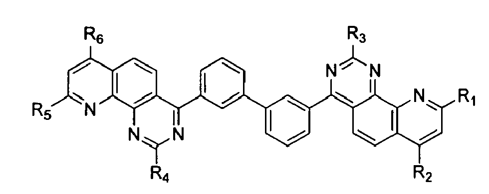
- Device 2 An inventive organic solar cell was made with the same layer structure as device 1 except that a 10 nm thick layer of 3,3'-bis(2,7,9-triphenylpyrido[3,2-h]quinazolin-4-yl)biphenyl was used instead of the BPhen layer. Under standard simulated AM1.5 the device shows a short circuit current of 8 mA/cm ⁇ 2, a FF of 42 % and an open circuit voltage of 0.50 V.
- the small differences in the characteristic photo conversion parameters are considered as normal fluctuations; basically the two devices have the same photoelectrical conversion performance. Both devices were submitted to thermal stress: the temperature was increased by 1 °C followed by a pause of 20 seconds and a I-V curve measurement. The procedure was repeated increasing the temperature by 1 °C in each step. The device 1 stopped to work at 67 °C, the I-V curve turned very flat, the FF dropped to 25 %. Device 2 kept working until 85 °C, after that the measurement was stopped.
- An OLED was fabricated with the following procedure: A glass substrate coated with ITO (90 nm thick, pre-patterned) was cleaned in organic solvents in conventional ultra-sound. Afterwards the substrate was treated with ozone plasma for 5 minutes. After the cleaning, the substrate was transferred to vacuum. The organic layers were deposited in high vacuum (base pressure lower than 10 ⁇ -3 Pa) by conventional VTE (Vacuum thermal evaporation). The deposited area was defined by a shadow mask, keeping some area of the ITO surface free so that an electrical contact for the measurements could (later on) be established.
- the organic layer sequence over the ITO layer is: 60 nm thick NPD layer doped with 2,2'-(perfluoronaphthalene-2,6-diylidene) dimalononitrile; 10 nm thick non-doped NPD layer, 20 nm thick emitter layer doped with Rubrene (10 % in weight); 10 nm ETL (structure 1 of table 1), 60 nm ETL (structure 1 of table 1) doped with W(hpp) 4 (10 % in weight). A 100 nm aluminum layer was deposited as Cathode. The OLED reached 1000 cd/m ⁇ 2 at 2,5 V.
- This OLED again reached 1000 cd/m ⁇ 2 at around 2,5 V.
- Both devices were submitted to thermal stress: the temperature was increased by 1 °C followed by a pause of 20 seconds and one I-V-L (current - voltage - luminance) curve measurement. The procedure was repeated increasing the temperature by 1 °C in each step. The device 4 stopped to work at 67°C. Device 3 kept working until 85°C, after that the measurement was stopped.
- doping refers to the electrical doping also called redox doping of a matrix semiconductor.
- P-doping increases the density of positive charge carriers (holes) and lowers the Fermi level in the semiconductor, towards the HOMO, the HOMO can also be considered as the valence band.
- N-doping increases the density of negative charge carriers (electrons) and raises the Fermi level in the semiconductor towards the LUMO, the LUMO can also be considered as the conduction band.
- Doping of a semiconductor increases its net charge carrier density and in consequence it increases its dark conductivity.
- the pure term doping refers to electrical doping and should not be confused with the emitter doping or any other form of mixture of two or more components that does not consists of an electrical doping.
Landscapes
- Chemical & Material Sciences (AREA)
- Organic Chemistry (AREA)
- Physics & Mathematics (AREA)
- Spectroscopy & Molecular Physics (AREA)
- Engineering & Computer Science (AREA)
- Materials Engineering (AREA)
- Electroluminescent Light Sources (AREA)
- Photovoltaic Devices (AREA)
Abstract
Description
- The present invention relates to bridged pyridoquinazoline and phenanthroline compounds and derivatives thereof, and to organic semiconducting materials and devices containing these compounds.
- Conjugated organic compounds have different applications. One important field comprises organic semiconductors. Organic semiconductors can be used to fabricate simple electronic components e.g. resistors, diodes, field effect transistors, and also optoelectronic components like light emitting devices (e.g. OLED), solar cells, and many others. Non-volatile and volatile, re-writable memories can be created using much different physical mechanism, such as molecular bi-stability, ferromagnetic properties (e.g.
US2006073658 ), ion transfer and charge wells (e.g.WO08125100 - A simple OLED is demonstrated in
US4356429A . There, between conductive electrodes, two semiconductive organic layers are brought together: one transporting holes and the other transporting electrons. The recombination of holes and electrons forms excitons in one or both of the organic layers, the excitons are eventually emitted following the spin statistics. Excitons with triplet spin can also be harvested by using the materials and techniques described inEP1705727 . More elaborated OLEDs are described inEP1804309 andUS2008182129 . - A simple, two layer, organic solar cell is described in
US4164431A . Many different solar cells use organic layers, for instance, Grätzel cells, polymer cells and small molecule solar cells. Many different approaches are tried out to increase the conversion performance; the so called bulk heterojunction solar cells have reached around 5 % conversion efficiency. - Conjugated organic compounds can be small molecules, for instance monomers, oligomers, polymers, copolymers, copolymers of conjugated and non-conjugated blocks, completely or partially cross-linked layers, aggregate structures, or brush like structures. A device made with different types of compounds, in different layers or mixed together, for example with polymer and small molecule layers, is also called a polymer - small molecule hybrid device.
- Organic electronic semiconductors can be used in organic electronic devices, and in organic-inorganic hybrid devices.
- Despite the large electronic gap usually up to 3 eV formed between the highest occupied molecular orbital (HOMO) and the lowest unoccupied molecular orbital (LUMO) of the molecule it is normally still low enough such that both positive and negative charge carriers can be injected by special electrodes. Typical organic semiconducting compounds may have a gap that is still high enough so that the compounds are optically active.
- Organic field effect transistors are explained, for example, in
US7026643 ,US2005146262 andUS2008230776 . The resistance of a semiconductive layer that is contacted by two electrodes (source and drain) can be controlled by the voltage that is applied to the gate. The gate is displaced on an insulator that is displaced parallel in contact to the semiconductive layer. Various geometries can be used, such as bottom gate (on the substrate), top gate (on the opposite side of the semiconductive layer relative to the substrate) or on both sides. Many different arrangements of layers can be used such as bipolar layers, injection layer, insulating layer between electrode and semiconductive layer to lower the off current, etc. - Different functional layers in different organic semiconductor devices request a variety of special characteristics.
- For instance OTFTs need high mobility materials in their active channel. Transparent circuits, such as transparent OTFTs require that the high mobility organic material also comprises a wide electronic band gap; the electric injection of holes and / or electrons must be still provided.
- Solar cells and OLEDs require transparent transport layers, with high conductivity. The transparency is necessary in those opto-electric devices to avoid non desired absorption of the light. These so called "window" materials can be used as transport layers, exciton or charge blocking layers. The thickness of the layers made with the window materials is used to adjust the micro cavity of the OLEDs and solar cells in such a way that the outcoupled emission of the OLED is a maximum, and in the case of the solar cell, the absorption and respective photocurrent of the device is a maximum. The non-optically active layers of all kinds of semiconductor devices can be exchanged for window materials in order to fabricate fully transparent components and circuits (e.g
US20060033115 ). - The functionality and nomenclature of the layers are typical as used in the field. Further explanation can be found in
US2006244370 . - Electronic devices also need high stability towards temperature, meaning that the intrinsic properties of the amorphous organic semiconducting materials, such as triphenyl amine derivatives, or phenantronine derivatives, must include a high glass transition temperature (Tg) and high temperature stability in the device.
- The conductivity can be, for example, measured by the so-called 2-point or 4-point-method. Here, contacts of a conductive material, such as gold or indium-tin-oxide, are disposed on a substrate. Then, the thin film to be examined is applied onto the substrate, so that the contacts are covered by the thin film. After applying a voltage to the contacts the current is measured. From the geometry of the contacts and the thickness of the sample the resistance and therefore the conductivity of the thin film material can be determined. The four point or two point method give the same conductivity values for doped layers since the doped layers grant a good ohmic contact.
- The temperature stability can be also measured with that method in that the (undoped or doped) layer is heated stepwise, and after a waiting period the conductivity is measured. The maximum temperature, which can be applied to the layer without loosing the desired semiconducting properties, is then the temperature just before the conductivity breaks down. For example, a doped layer can be heated on the substrate with two electrodes, as disclosed above, in steps of 1°C, wherein after each step there is a waiting period of 10 seconds. Then the conductivity is measured. The conductivity changes with temperature and breaks down abruptly at a particular temperature. The temperature stability is therefore the temperature up to which the conductivity does not break down abruptly. The measurement is performed in vacuum.
- The properties of the many different used materials can be described by the position of their highest occupied molecular orbital energy level (HOMO, synonym of ionization potential), and the lowest unoccupied molecular orbital energy level (LUMO, synonym of electro affinity).
- A method to determine the ionization potentials (IP) is the ultraviolet photo spectroscopy (UPS). It is usual to measure the ionization potential for solid state materials; however, it is also possible to measure the IP in the gas phase. Both values are differentiated by their solid state effects, which are, for example the polarization energy of the holes that are created during the photo ionization process (N. Sato et al., J.. Chem. Soc. Faraday Trans. 2, 77, 1621 (1981)). A typical value for the polarization energy is approximately 1 eV (E.V. Tsiper et al., Phys. Rev. B 195124 (2001)), but larger discrepancies of the values can also occur (N. Sato et al., J. Chem. Soc. Faraday Trans 2, 77, 1621 (1981)). The IP is related to beginning of the photoemission spectra in the region of the large kinetic energy of the photoelectrons, i.e. the energy of the most weakly bounded electrons. A related method to UPS, the inverted photo electron spectroscopy (IPES) can be used to determine the electron affinity (EA) (see e.g. W. Gao et. al, Appl. Phys. Lett. 82, 4815 (2003). However, this method is less common. Electrochemical measurements in solution are an alternative to the determination of solid state oxidation (Eox) and reduction (Ered) potential. An adequate method is for example the cyclo-voltammetry (e.g. J.D. Anderson, J. Amer. Chem. Soc. 120, 9646 (1998)). Empiric methods for the extraction of the solid state ionization potentials are known from the literature. (e.g.. B.W. Andrade et al., Org. Electron. 6, 11 (2005); T.B. Tang, J. Appl. Phys. 59, 5 (1986); V.D. Parker, J. Amer. Chem. Soc. 96, 5656 (1974); L.L. Miller, J. Org. Chem. 37, 916 (1972), Y. Fu et al., J. Amer. Chem. Soc. 127, 7227 (2005)). There are no known empiric equations for the conversion of reduction potentials into electro affinities. The reason for that is difficulty of the determination of the electro affinity. Therefore, a simple rule is used very often: IP=4.8 eV+ e*Eox (vs. Ferrocen/Ferrocenium) and EA=4.8eV +e*Ered (vs. Ferrocen/Ferrocenium) respectively (see B.W. Andrade, Org. Electron. 6, 11 (2005) and Refs. 25-28 therein). Processes are known for the correction of the electrochemical potentials in the case other reference electrodes or other redox pair are used (see A.J. Bard, L.R. Faulkner, "Electrochemical Methods: Fundamentals and Applications", Wiley, 2. Ausgabe 2000). The information about the influence of the solution used can be found in N.G. Connelly et al., Chem. Rev. 96, 877 (1996). It is usual, even if not exactly correct to use the terms "Energy of the HOMO" E(HOMO) and "energy of the LUMO" E(LUMO) respectively as synonyms for the ionization energy and electro affinity (Koopmans Theorem). It has to be taken in consideration, that the ionization potentials and the electron affinities are given in such a way that a larger value represents a stronger binding of a released or respectively of an absorbed electron. The energy scale of the molecular orbitals (HOMO, LUMO) is opposed to this. Therefore, in a rough approximation, is valid: IP=-E(HOMO) und EA=-E(LUMO). The given potentials correspond to the solid-state potentials. Hole transport layers, including the respective blockers, mostly have HOMO in the range from 4,5 to 5,5 eV (below the vacuum level) and LUMO in the range of 1.5 eV to 3 eV. The HOMO levels of the emitter materials are in the range of 5 eV to 6.5 eV, and the LUMO in the range from 2 to 3 eV. Electron transport materials, including their respective blockers, have their HOMO in range of 5,5 eV to 6.8 eV and LUMO in the range of 2,3 eV to 3.3 eV, larger (lower laying) LUMO and HOMO levels may be required for solar cells. The work function of the contact materials is around 4 to 5 eV for the anode and 3 to 4.5 eV for the cathode.
- The performance characteristics of (opto)electronic multilayered components are determined from the ability of the layers to transport the charge carriers, amongst others. In the case of light-emitting diodes, the ohmic losses in the charge transport layers during operation are associated with their conductivity. The conductivity directly influences the operating voltage required and also determines the thermal load of the component. Furthermore, depending on the charge carrier concentration in the organic layers, bending of the band in the vicinity of a metal contact results which simplifies the injection of charge carriers and can therefore reduce the contact resistance. Similar deliberations in terms of organic solar cells also lead to the conclusion that their efficiency is also determined by the transport and extraction to the electrode properties of charge carriers.
- By electrically doping hole transport layers with a suitable acceptor material (p-doping) or electron transport layers with a donor material (n-doping), respectively, the density of charge carriers in organic solids (and therefore the conductivity) can be increased substantially. Additionally, analogous to the experience with inorganic semiconductors, applications can be anticipated which are precisely based on the use of p- and n-doped layers in a component and otherwise would be not conceivable. The use of doped charge-carrier transport layers (p-doping of the hole transport layer by admixture of acceptor-like molecules, n-doping of the electron transport layer by admixture of donor-like molecules) in organic light-emitting diodes is described in
US2008203406 andUS 5,093,698 . -
US2008227979 discloses in detail the doping of organic transport materials, also called matrix, with inorganic and with organic dopants. Basically, an effective electronic transfer occurs from the dopant to the matrix increasing the Fermi level of the matrix. For an efficient transfer in a p-doping case, the LUMO energy level of the dopant must be lower laying or at least slightly higher, not more than 0.5 eV, to the HOMO energy level of the matrix. For the n-doping case, the HOMO energy level of the dopant must be higher laying or at least slightly lower, not lower than 0.5 eV, to the LUMO energy level of the matrix. It is furthermore desired that the energy level difference for energy transfer from dopant to matrix is smaller than + 0.3 eV. - The dopant donor is a molecule or a neutral radical or combination thereof with a HOMO energy level (ionization potential in solid state) lower than 3.3 eV, preferably lower than 2,8 eV, more preferably lower than 2.6 eV and its respectively gas phase ionization potential is lower than 4.3 eV, preferably lower than 3.8 eV, more preferably lower than 3.6 eV. The HOMO of the donor can be estimated by ciclo-voltametric measurements. An alternative way to measure the reduction potencial is to measure the cation of the donor salt. The donor has to exhibit an oxidation potential that is smaller or equal than -1.5 V vs Fc / Fc+ (Ferrum/Ferrocenium redox-pair), preferably smaller than -1.5 V, more preferably smaller or equal than approximately -2.0 V, even more preferably smaller or equal than -2.2 V. The molar mass of the donor is in a range between 100 and 2000 g/mol, preferably in a range from 200 and 1000 g / mol. The molar doping concentration is in the range of 1:0000 (dopant molecule : matrix molecule) and 1:2, preferably between 1:00 and 1:5, more preferably between 1:100 and 1:10. In individual cases doping concentrations larger than 1:2 are applied, e.g. if large conductivities are required. The donor can be created by a precursor during the layer forming (deposition) process or during a subsequent process of layer formation (see
DE 10307125.3 ). The above given value of the HOMO level of the donor refers to the resulting molecule or molecule radical. - A dopant acceptor is a molecule or a neutral radical or combination thereof with a LUMO level larger than 4.5 eV, preferably larger than 4.8 eV, more preferably larger than 5.04 eV. The LUMO of the acceptor can be estimated by cyclo-voltammetric measurements. The acceptor has to exhibit a reduction potential that is larger or equal than approximately -0.3 V vs Fc / Fc+ (Ferrum/Ferrocenium redox-pair), preferably larger or equal than 0.0 V, preferably larger or equal than 0.24 V. The molar mass of the aceptor is preferably in the range of 100 to 2000 g / mol, more preferably between 200 and 1000 g / mol, and even more preferably between 300 g/mol and 2000 g/mol. The molar doping concentration is in the range of 1:0000 (dopant molecule : matrix molecule) and 1:2, preferably between 1:00 and 1:5, more preferably between 1:100 and 1:10. In individual cases doping concentrations larger than 1:2 are applied, e.g. if large conductivities are required. The acceptor can be created by a precursor during the layer forming (deposition) process or during a subsequent process of layer formation. The above given value of the LUMO level of the acceptor refers to the resulted molecule or molecule radical.
- Typical examples of doped hole transport materials are: copperphthalocyanine (CuPc), which HOMO level is approximately 5.2 eV, doped with tetrafluoro-tetracyanoquinonedimethane (F4TCNQ), which LUMO level is about 5.2 eV; zincphthalocyanine (ZnPc) (HOMO = 5.2 eV) doped with F4TCNQ; pentacene, with its HOMO around 4.6 eV, doped with tris { 2, 5 - bis ( 3, 5 - bis - trifluoromethyl - phenyl) - thieno } [ 3, 4 - b, h, n] - 1, 4, 5, 8, 9, 12 - hexaazatriphenylene, which has its LUMO level at about 4.6 eV; α-NPD doped with 2,2'-(perfluoronaphthalene-2,6-diylidene) dimalononitrile.
- Typical examples of doped electron transport materials are: fullerene C60 doped with acridine orange base (AOB); perylene-3,4,9,10-tetracarboxylic-3,4,9,10-dianhydride (PTCDA) doped with leuco crystal violet; 2,9 - di (phenanthren-9-yl) - 4,7 - diphenyl - 1,10 - phenanthroline doped with Tetrakis ( 1,3,4,6,7,8 - Hexahydro - 2H - pyrimido [ 1,2 - a] pyrimidinato) ditungsten (II) (W(hpp)4); naphthalene tetracarboxylic acid di-anhydride (NTCDA) doped with 3,6-bis-(dimethyl amino)-acridine; NTCDA doped with bis(ethylene-. dithio) tetrathiafulvalene (BEDT-TTF).
- There is a technical challenge to provide electron transport materials (ETM) and emitter host (EMH) materials that have a sufficiently low laying LUMO level so that they can be doped, and still have a enough high laying LUMO level which can efficiently transfer charge to emitter host (in case of an ETM) and transfer energy to the emitter dopant (in case of EMH). The limitation for high laying LUMO level of the ETL is given by the dopability, since the n-dopants with very high HOMO tend to be unstable; also the injection is difficult for very high LUMO of the ETL.
- A technical challenge for organic solar cells is to provide electron transport materials with low laying LUMO level that can easily align with the LUMO of the heterojunction acceptor of the solar cell. Furthermore, materials are required with the low laying LUMO level and a very low laying HOMO level that can be used to block holes.
- It is an object of the present invention to provide a new class of functional materials which can be utilized in organic semiconducting materials to overcome the drawbacks of the prior art. It is a further object of the invention to provide organic semiconducting materials that are transparent. Another object of the invention is to provide thermally stable matrix materials. It is an additional object of the invention to provide dopable matrix materials. It is also an object to provide doped and thermally stable matrix materials. Further, combinations of the object are highly desired, such as a dopable window electron transport layer with high glass transition temperature which may be used in semiconducting layers and in electronic devices.
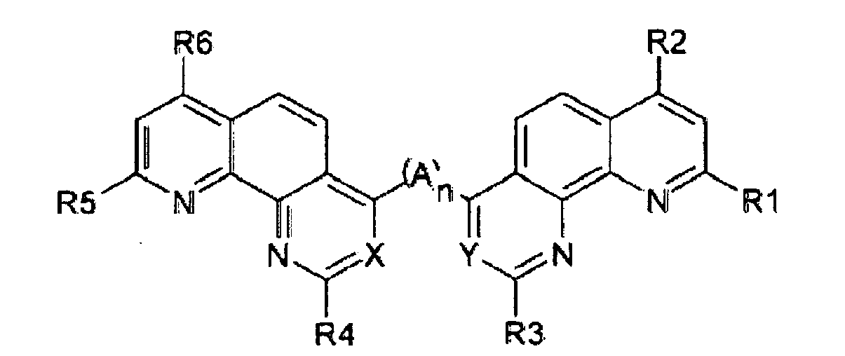
- These objects are achieved by a compound according to formula:

R1 and R2 and R5 and R6 are independently selected from aryl, heteroaryl, alkyl having the formula CHR2 or alkyl having the formula CR3 with R= C1-C20-alkyl;
R3 and R4 are independently selected form H, substituted or unsubstituted aryl, heteroaryl, alkyl having 1 to 20 carbon atoms, cycloalkyl having 3 to 20 carbon atoms, NH2, NHR0, NR0 2 with R0 = substituted or unsubstituted aryl, heteroaryl, alkyl with 1 to 20 carbon atoms, cycloalkyl, N as member of cyclic amines, carbazolyl, dibenzazepinyl, O-alkyl or O-aryl;
and A is a spacer selected from aryl, heteroaryl or alkyl, and wherein n is 0 or 1. - Thus, in one embodiment, A does not have to be present at all, and the ring structures are directly connected via a single bond.
- Preferably, A is selected from


- Preferably, X and Y are: N or C-CN
More preferably, at least one of X and Y is N.
More preferably, R1-R6 are phenyl.
Even preferred, R1-R6 are substituted aryl, and/or the spacer A is substituted. - Also preferred are compounds as follows:


- According to the invention is also an organic semiconducting material comprising at least one organic matrix material which is optionally doped with at least one dopant, wherein the matrix material comprises a compound according to the invention.
- The object is achieved also by an electronic, optoelectronic or electroluminescent element having an electronically functionally effective region, wherein the electronically effective region comprises at least one compound according to the invention.
- Preferably, the electronic, optoelectronic or electroluminescent element is in the form of an organic light-emitting diode, a field effect transistor, a photo detector or an organic solar cell.
- In a light-emitting diode the inventive materials can be used in electron transport layers, which might be optionally doped. The inventive materials can be also used in light-emitting diodes in interlayers such as hole blocking layers. Further, for organic solar cells, the materials may be used to provide stable electron transport layers (ETL), wherein the ETLs can be further doped. Additionally, the invention provides stable materials for buffer layers for solar cells that can be doped or undoped.
- According to the invention, especially a window semiconducting organic material is provided that can be electrically doped achieving a high conductivity while it remains highly transparent in the visible spectra and has a high thermal stability.
- According to the invention, also an organic field-effect transistor may be provided comprising at least one inventive material for use in a transport layer. An organic field effect transistor may also comprise at least one material of the invention as electronically inert buffer layer, when no charge is injected due to high potential barrier. An organic field effect transistor may also comprise at least one material of the invention as doped injection layer.
- Provided can be also a doped pn-transition in an organic electronic element, for combining stacked organic light-emitting diodes, stacked solar cells and converting contacts to an electrode, respectively, as is, for example, known from
EP 1 804 308 orEP 1 808 910 . pn-transitions in OLEDs are also called charge generation layer or connection unit. pn-transitions in organic solar cells are also called recombination layer. - Typically, the organic layer arrangement of an OLED or an solar cell comprises several organic layers which are stacked. Within one organic layer arrangement there may be also provided one or more pn-transitions, such as is known for stacked OLEDs (see
EP 1 478 025 A2 ), wherein such a pn-transition is formed in one embodiment by means of a p-doped hole transport layer and an n-doped electron transport layer which are in direct contact with one another. Such a pn-transition provides a structure generating electric charges, in which, when applying an electrical potential, electrical charges are generated, preferred in the boarder area between both layers. - In solar cells and photo sensors the pn-transition is also utilized to combine stacked hetero junctions and to, thus, add voltage generated by this element (
US 2006 027 834 A ). The transitions have the same function as tunnel-transitions in stacked inorganic heterojunction solar cells, although the physical mechanisms are different. - The transitions are also used to achieve an improved injection (extraction for solar cells) to the electrodes (
EP 1 808 910 ). - For improving the energetic properties in an organic electronic element it was suggested in
WO 2005/109 542 A1 to form a pn-transition with one layer of an organic semiconducting material of n-type and one layer of an organic material of p-type, wherein the layer of the organic semiconducting material of n-type is in contact with an electrode formed as an anode. By this, an improved injection of charge carriers in the form of holes into the layer of the organic semiconducting material of p-type is achieved. - In order to stabilize the pn-transition there is utilized one layer of a different material as interlayer. Such stabilized pn-transitions are for example disclosed in
US 2006040132 A . There a metal is utilized as interlayer. OLEDs having a metal layer have a lower lifetime due to the diffusion of the metal atoms. - Utilizing the inventive compounds stable interlayers and doped interlayers between pn-transitions can be provided, in order to form stabile organic semiconducting elements. Here, it is known that such a pn-transition functions very efficiently, if both materials of p-and n-type are doped.
- It is also possible to provide a material and a material combination, in order to result in an efficient and stable, mainly thermally stable pn-transition.
- The compounds of this invention can be used in OLEDs in electron transport layers as a neat layer, or as a doped layer in combination with a redox dopant. The compounds can also be used in mixture with other electron transport materials, other hole transport materials or other functional materials such as emitter dopants. The compounds can be used as hole blocking layers. Advantageous effects are seen over the prior art since the materials have a higher glass transition temperature compared to materials described in the prior art, such as in
DE 10 2007 012 794EP 07 400 033.2 - The prior art deals with electron transporting materials that can be doped in order to improve their conductivity in an OLED layer, for example. Those materials' substitution patterns strongly influence their final conductivity, as well as their thermal properties (melting points, sublimation temperatures and glass transition temperatures). It was found that the electronic properties are mainly governed by the core structure of a defined class of materials. The surrounding chemical groups can though be employed to alter the photo-physical properties: Melting point, solubility, decomposition temperature, sublimation temperature, glass transition temperature, etc..
- Additional features and advantages of the invention can be taken from the following detailed description of preferred embodiments, together with the drawings as attached.
-
-
Fig. 1 shows a cross section of a typical small molecule OLED. -
Fig. 2 shows a cross section of a typical small molecule organic solar cell. - The new conjugated organic compound of this invention is especially suitable for use in organic light emitting diodes.
Fig. 1 shows a typical layer structure of an organic light emitting diode. The layers are disposed on a substrate (10) in the following order: anode (11), p-doped hole transport layer (12), electron blocking layer (13), emission layer (14), hole blocking layer (15), n-electron transport layer (16), and cathode (17). Two or more layers can collapse into a smaller number of layers if properties can be combined. Inverted structure and multiple stacked OLEDs are also well known in the field. The emission layer is usually composed by an emitter matrix material and an emitter dopant; this layer can be also composed by several other layers to generate light with a broad spectrum combining several emitters, for example, to generate white light. -
Fig.2 shows a typical small molecule organic solar cell. Many variations are possible. One simple structure that offers reasonable efficiencies is composed by a substrate (20), followed by: anode (21), p-doped hole transport layer (22), thin interlayer that is non-doped (23), the photo-active bulk-heterojunction (24), and electron transport layer (25), a buffer layer (26), and the cathode (27). - It was surprisingly found that especially the thermal stability of doped layers can be significantly increased utilizing the compounds according to the present invention as matrix material. Especially, a glass transition temperature of about 200 °C was achieved with the compound of structure 1, whereas for compounds of the prior art, as can be taken from
DE 10 2007 012 794EP 07400033.2 -

- The syntheses of the claimed materials are common until the 3rd synthetic step (synthesis of 6,7-dihydro-2,4-diphenylchinolin-8(5H)-one, see below). The spacer (A) is introduced first by the use of the appropriate di-aldehyde (taken out of the following list, for instance: thiophene dicarboxaldehyde, pyrrole dicarboxaldehyde, pyridine dicarboxaldehyde, oxadiazole dicarboxaldehyde, anthracene dicarboxaldehyde, diphenyl dicarbioxaldehyde phenyl dicarboxaldehyde, all of them with a selected substitution pattern) at the 4th step. This di-aldehyde is either commercially available or prepared by classical methods. The X and Y groups are selected by choosing the appropriate reagent at the 5th step (benzimidiniumchloride for X or Y = N, or 3-amino-3-phenylacrylonitrile when X or Y = CN, both commercially available). The last oxidation step is common for all the claimed materials, using Palladium on coal as oxidant under reflux in a high boiling point solvent.
-

-

- The pyrylium salts dissolved after addition, and a yellow compound precipitated after a few hours. After 7 hours is the precipitate thicker. The reaction was cooled to room temperature.
- The voluminous precipitate was filtrated using a Büchner paper filter and washed portionwise with 250 mL methanol. The yellow powder was dried in a vacuum-oven overnight at 50°C.
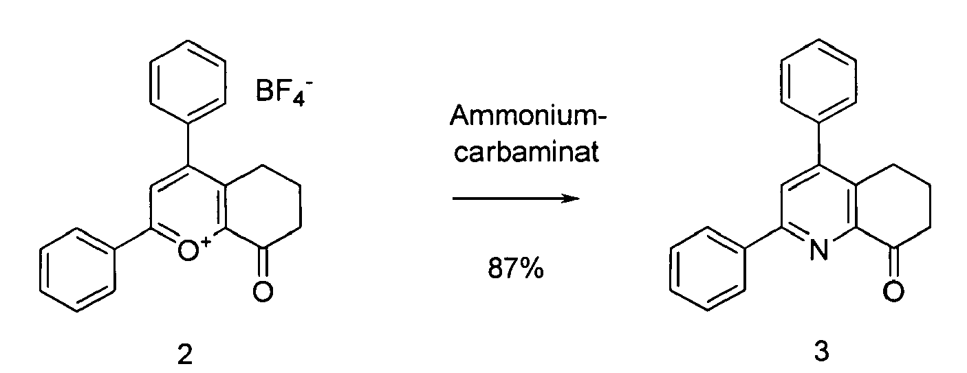
- Second step: Synthesis of 5,6,7,8-tetrahydro-8-oxo-2,4-diphenyl-1-benzopyrylium-tetrafluoroborate (2). All manipulations were carried out in air, without any further purification of commercial solvents/chemicals.

- A mixture of 5,6-dihydro-2-phenacyl-2,4-diphenyl-2H,7H-1-benzopyran-8-one (1) and 170 mL BF3.MeOH complex (1.3 mol.L-1) in 300 mL di-n-butylether was heated to 90°C. The reaction medium quickly turned red and the voluminous precipitate solubilised for a short time before precipitating again as a fine deep-red powder. The suspension was kept refluxing for 1h and cooled to room temperature.
- 200 mL diethylether were added through the cooler under strong agitation providing a bigger amount of precipitate. The suspension was then cooled using an ice bath and agitated for two hours. The suspension was filtered using a Büchner apparatus and washed portionwise with 250 mL diethylether. The red powder is then dried using a vacuum oven at 50°C.
The filtrate solution was not kept any further.
Melting Point: 213°C - Third step: Synthesis of 6,7-dihydro-2,4-diphenylchinolin-8(5H)-one (3). All manipulations were carried out in air, without any further purification of commercial solvents/chemicals.
- The precipitate is filtered, using a Büchner paper filter, and washed with 475 ml water, and dried. The purple powder is suspended in 30 mL methanol and mixed with 240 mL diethylether. The mixture was agitated for 1 hour and filtered with a paper filter. The red-purple filtrate was not kept and the crème-powder was washed portionwise with diethylether and dried in a vacuum oven at 50°C.
Melting Point: 178°C - Fourth step: Synthesis of 7,7'-(1,3-phenylenebis(methan-1-yl-1-ylidene))bis(2,4-diphenyl-6,7-dihydroquinolin-8(5H)-one) (4). All manipulations were carried out in air, without any further purification of commercial solvents/chemicals.

- To a mixture of 6,7-dihydro-2,4-diphenylchinolin-8(5H)-one (3) (66,8mmol) and isophthalaldehyde (334 mmol) in 300 mL methanol was added under stirring potassium hydroxide (8.2 g in 70 mL Water). The suspension was stirred for 10 h at 100°C.
- After two days the reaction was neutralised with 20 mL acetic acid and stirred for 30 min. The precipitate was then filtered using a Buchner filter and washed with 700 mL water. The white powder was suspended in 100 mL Methanol and sonicated for 10 min at room temperature (4 times). The powder was dried using a vacuum oven at 50 °C.
- Fifth step: Synthesis of 1,3-bis(2,7,9-triphenyl-1,4,5,6-tetrahydropyrido[3,2-h]quinazolin-4-yl)benzene (5). All manipulations were carried out in air, Absolute Ethanol was freshly distilled before manipulation.

- A mixture of (7E,7'E)-7,7'-(1,3-phenylenebis(methan-1-yl-1-ylidene))bis(2,4-diphenyl-6,7-dihydroquinolin-8(5H)-one) (4) (14.3 mmol) and benzimidiniumchloride-monohydrate (35.8 mmol) in 260 mL absolute ethanol was heated to reflux, then a solution of 9.6 g potassium tert-butylate in 120 mL absolute ethanol was added dropwise while stirring and refluxing. A white precipitate appeared after 6 hours and became thicker as the reaction proceeded. After 62 hours the reaction was cooled to room temperature, and worked up.
- The mixture was neutralized with acetic acid (20 mL). Water was added (300mL), and a precipitate appeared. 300mL chloroform was added to solubilize the precipitate and obtain two phases. The mixture was stirred for 30 minutes at room temperature. The organic phase was separated and the water phase extracted once again with 100 mL chloroform. The organic phases were combined and dried with magnesium sulfate. All volatiles were evaporated and the residues washed with ether to obtain a light brown powder.
- Sixth step: Synthesis of 1,3-bis(2,7,9-triphenylpyrido[3,2-h]quinazolin-4-yl)benzene (6). All manipulations were carried out in air, without any further purification of commercial solvents/chemicals.

- A suspension of 1,3-bis(2,7,9-triphenyl-1,4,5,6-tetrahydropyrido[3,2-h]quinazolin-4-yl)benzene (5) (4.4 mmol) in 220 diethyleneglycol was heated until total dissolution. 1.2 g Pd/C was then slowly added, and the reaction was refluxed for 6 hours with argon bubbling directly in the solution. The reaction was then stopped, and the suspension cooled to room temperature.
- 600mL distilled water was then added and stirred an additional 30 min, a precipitate appeared and was filtered through celite on a fritt (porosity 4). The filtrate was discarded. The black solid was then washed portionwise with 600 mL Chloroform until chloroform filtrate became colorless. The resulting yellow-greenish solution was dried with MgSO4 and filtered through a paper filter. The solvents were then reduced to approx 30mL using a Rotavapor. 50 mL was added then at room temperature, so that a yellow precipitate was obtained. The suspension was filtered, and the solid suspended in n-hexane and sonicated for 15 minutes. The suspension was filtered again and suspended in 30 mL diethylether and sonicated again for 15 min. The suspension was filtered and dried finally.
-

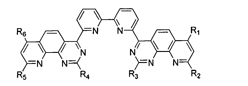
- Fourth step: Synthesis and work up are the same as in example 1, isophthalaldehyde is replaced by pyridine-2,6-dicarbaldehyde.

-

-

-

-

-

-

-

- R1-R6=Ph
-

-

-

-
- R1-R6=Ph
-

-

-

-
-

-

-

-

- Steps 1 to 4 are the same as for example 1.
-

- A mixture of (7E,7'E)-7,7'-(1,3-phenylenebis(methan-1-yl-1-ylidene))bis(2,4-diphenyl-6,7-dihydroquinolin-8(5H)-one) (4) (6.6 mmol) and 3-amino-3-phenylacrylonitrile (2.5 g, 17.1 mmol) in 50 mL absolute ethanol was heated to reflux, then a solution of 3.2 g potassium tert-butylate in 30 mL absolute ethanol was added dropwise while stirring and refluxing. A white precipitate appeared after 6 hours and became thicker as the reaction proceeded. After 24 hours the reaction was cooled to room temperature, and worked up.
- The mixture was neutralized with acetic acid (10mL), a precipitate appeared and was filtered using a Büchner paper filter and washed with 300 mL water and three times sonicated in suspension in 25 mL ethanol (15 minutes each time). The light beige powder was dried in a vacuum oven at 60 °C.
-

- A suspension of 4,4'-(1,3-phenylene)bis(2,7,9-triphenyl-1,4,5,6-tetrahydro-1,10-phenanthroline-3-carbonitrile) (5) in 2L diethyleneglycol was heated until total dissolution. 10 g Pd/C was then slowly added, and the reaction was refluxed for 72 hours with argon bubbling directly in the solution. The reaction was monitored by TLC (Silica Gel ; CH2Cl2). The starting material's spot (rf: 0.8, blue-green under 366 nm) converted into a blue fluorescent spot (rf: 0.9). Once the starting material spot has disappeared, the reaction was stopped, and the suspension cooled to room temperature.
- 800 mL distilled water was then added and stirred an additional 30 min and filtered through a fritt (porosity 4). The black residue on the fritt was washed portionwise with 2 L water and dried on the fritt. The filtrate was discarded. The black solid was then washed portionwise with 6 L chloroform. The resulting yellow-greenish solution was dried with MgSO4 and filtered through a paper filter. The solvents were then removed using a Rotavapor. The residue was washed several times with 1L cylcohexane and 500 mL diethylether. 14 g (85 %) white powder was obtained.
- Device 1 (comparative). A state of the art organic solar cell was fabricated with the following procedure: patterned glass substrate coated with ITO was cleaned in an ultrasound bath with etanol, acetone and isopropanol. Afterwards the ITO substrate was exposed to oxygen plasma treatment for 15 minutes. The substrate was loaded into the vacuum trough a glove box with nitrogen. In vacuum the organic layers were deposited with conventional VTE (vacuum thermal evaporation). First a 10 nm thick 5% (molar) F4-TCNQ doped CuPc layer was deposited through a shadow mask over the ITO. A 10 nm undoped CuPc layer was deposited over the doped CuPc layer. A 30 nm thick mixed layer of fullerene C60 and CuPc was deposited with a molar ratio of 2(C60):1(CuPc). A 40 nm thick C60 layer was deposited on top of the mixed layer. A 10 nm BPhen (4,7-diphyenyl-1,10-phenanthroline) layer was deposited on top of the C60 layer. The BPhen layer is followed by a 100 nm thick A1 cathode. Under standard simulated AM1.5 normal the device shows a short circuit current of 8 mA/cm^2, a FF of 41 % and an open circuit voltage of 0.51 V.
- Device 2. An inventive organic solar cell was made with the same layer structure as device 1 except that a 10 nm thick layer of 3,3'-bis(2,7,9-triphenylpyrido[3,2-h]quinazolin-4-yl)biphenyl was used instead of the BPhen layer. Under standard simulated AM1.5 the device shows a short circuit current of 8 mA/cm^2, a FF of 42 % and an open circuit voltage of 0.50 V.
- The small differences in the characteristic photo conversion parameters are considered as normal fluctuations; basically the two devices have the same photoelectrical conversion performance. Both devices were submitted to thermal stress: the temperature was increased by 1 °C followed by a pause of 20 seconds and a I-V curve measurement. The procedure was repeated increasing the temperature by 1 °C in each step. The device 1 stopped to work at 67 °C, the I-V curve turned very flat, the FF dropped to 25 %. Device 2 kept working until 85 °C, after that the measurement was stopped.
- An OLED was fabricated with the following procedure: A glass substrate coated with ITO (90 nm thick, pre-patterned) was cleaned in organic solvents in conventional ultra-sound. Afterwards the substrate was treated with ozone plasma for 5 minutes. After the cleaning, the substrate was transferred to vacuum. The organic layers were deposited in high vacuum (base pressure lower than 10^-3 Pa) by conventional VTE (Vacuum thermal evaporation). The deposited area was defined by a shadow mask, keeping some area of the ITO surface free so that an electrical contact for the measurements could (later on) be established. The organic layer sequence over the ITO layer is: 60 nm thick NPD layer doped with 2,2'-(perfluoronaphthalene-2,6-diylidene) dimalononitrile; 10 nm thick non-doped NPD layer, 20 nm thick emitter layer doped with Rubrene (10 % in weight); 10 nm ETL (structure 1 of table 1), 60 nm ETL (structure 1 of table 1) doped with W(hpp)4 (10 % in weight). A 100 nm aluminum layer was deposited as Cathode. The OLED reached 1000 cd/m^2 at 2,5 V.
- The device was fabricated as device 3, but the ETL was replaced by the following structure.

- This OLED again reached 1000 cd/m^2 at around 2,5 V.
- Both devices (device 3 and Device 4) were submitted to thermal stress: the temperature was increased by 1 °C followed by a pause of 20 seconds and one I-V-L (current - voltage - luminance) curve measurement. The procedure was repeated increasing the temperature by 1 °C in each step. The device 4 stopped to work at 67°C. Device 3 kept working until 85°C, after that the measurement was stopped.
- The term doping refers to the electrical doping also called redox doping of a matrix semiconductor. P-doping increases the density of positive charge carriers (holes) and lowers the Fermi level in the semiconductor, towards the HOMO, the HOMO can also be considered as the valence band. N-doping increases the density of negative charge carriers (electrons) and raises the Fermi level in the semiconductor towards the LUMO, the LUMO can also be considered as the conduction band. Doping of a semiconductor increases its net charge carrier density and in consequence it increases its dark conductivity. The pure term doping refers to electrical doping and should not be confused with the emitter doping or any other form of mixture of two or more components that does not consists of an electrical doping.
- The features disclosed in the foregoing description, the claims and the accompanying drawings may both separately and in any combination thereof be material for realizing the invention in diverse forms thereof.
Claims (9)
- Compound according to formula:

R1 and R2 and R5 and R6 are independently selected from aryl, heteroaryl, alkyl having the formula CHR2 or alkyl having the formula CR3 with R= C1-C20-alkyl;
R3 and R4 are independently selected form H, substituted or unsubstituted aryl, heteroaryl, alkyl having 1 to 20 carbon atoms, cycloalkyl having 3 to 20 carbon atoms, NH2, NHR0, NR0 2 with R0 = substituted or unsubstituted aryl, heteroaryl, alkyl with 1 to 20 carbon atoms, cycloalkyl, N as member of cyclic amines, carbazolyl, dibenzazepinyl, O-alkyl or O-aryl;
and A is a spacer selected from aryl, heteroaryl or alkyl, and wherein n is 0 or 1. - Compound according to claim 1, wherein A is selected from


- Compound according to claim 1 or 2, wherein X is N or C-CN.
- Compound according to any of the preceding claims, wherein at least one of X and Y is N.
- Compound according to any of the preceding claims, wherein R1-R6 are substituted aryl and/or spacer A is substituted.
- Compound according to any of claims 1-4, wherein R1-R6, are phenyl.
- Organic semiconducting material comprising at least one organic matrix material which is optionally doped with at least one dopant, wherein the matrix material comprises a compound according to any of claims 1 to 6.
- Electronic, optoelectronic or electroluminescent device having an electronically functionally effective region, wherein the electronically effective region comprises at least one compound according to claims 1 to 6.
- Electronic, optoelectronic or electroluminescent element according to claim 8 in the form of an organic light-emitting diode, a field effect transistor, a photo detector or an organic solar cell.
Priority Applications (3)
| Application Number | Priority Date | Filing Date | Title |
|---|---|---|---|
| EP08020941A EP2194055B1 (en) | 2008-12-03 | 2008-12-03 | Bridged pyridoquinazoline or phenanthroline compounds and organic semiconducting material comprising that compound |
| US13/132,557 US8475686B2 (en) | 2008-12-03 | 2009-12-02 | Bridged pyridoquinazoline or phenanthroline compounds and organic semiconducting material comprising that compound |
| PCT/EP2009/008597 WO2010063461A1 (en) | 2008-12-03 | 2009-12-02 | Bridged pyridoquinazoline or phenanthroline compounds and organic semiconduting material comprising that compound |
Applications Claiming Priority (1)
| Application Number | Priority Date | Filing Date | Title |
|---|---|---|---|
| EP08020941A EP2194055B1 (en) | 2008-12-03 | 2008-12-03 | Bridged pyridoquinazoline or phenanthroline compounds and organic semiconducting material comprising that compound |
Publications (2)
| Publication Number | Publication Date |
|---|---|
| EP2194055A1 true EP2194055A1 (en) | 2010-06-09 |
| EP2194055B1 EP2194055B1 (en) | 2012-04-04 |
Family
ID=40420118
Family Applications (1)
| Application Number | Title | Priority Date | Filing Date |
|---|---|---|---|
| EP08020941A Ceased EP2194055B1 (en) | 2008-12-03 | 2008-12-03 | Bridged pyridoquinazoline or phenanthroline compounds and organic semiconducting material comprising that compound |
Country Status (3)
| Country | Link |
|---|---|
| US (1) | US8475686B2 (en) |
| EP (1) | EP2194055B1 (en) |
| WO (1) | WO2010063461A1 (en) |
Cited By (5)
| Publication number | Priority date | Publication date | Assignee | Title |
|---|---|---|---|---|
| EP2452946A1 (en) | 2010-11-16 | 2012-05-16 | Novaled AG | Pyridylphosphinoxides for organic electronic device and organic electronic device |
| EP2448031A3 (en) * | 2010-10-26 | 2013-05-01 | Fujifilm Corporation | Photoelectric conversion device and solid-state imaging device |
| CN106025090A (en) * | 2015-03-25 | 2016-10-12 | 乐金显示有限公司 | Organic light emitting display device |
| CN110190195A (en) * | 2019-05-16 | 2019-08-30 | 华南理工大学 | A kind of perovskite photovoltaic-based on compound interface transmission material shines-optical detection multifunction device and preparation method thereof |
| US20260114109A1 (en) * | 2024-10-23 | 2026-04-23 | Angelee Kang | Hybrid solar cell and method for manufacturing same |
Families Citing this family (6)
| Publication number | Priority date | Publication date | Assignee | Title |
|---|---|---|---|---|
| EP2367215A1 (en) * | 2010-03-15 | 2011-09-21 | Novaled AG | An organic photoactive device |
| EP3017641B1 (en) * | 2013-11-12 | 2019-10-02 | Huawei Technologies Co., Ltd. | System and method for high efficiency wireless local area network communications |
| KR101734459B1 (en) * | 2014-05-20 | 2017-05-11 | 제일모직 주식회사 | Organic compound and composition and organic optoelectric device and display device |
| CN111100146B (en) * | 2019-12-30 | 2021-01-22 | 陕西莱特光电材料股份有限公司 | Organic compound, application and organic electroluminescent device using organic compound |
| KR102966932B1 (en) | 2020-05-12 | 2026-05-20 | 삼성디스플레이 주식회사 | Organic electroluminescence device and compound for organic electroluminescence device |
| CN115925530B (en) * | 2022-07-01 | 2024-03-12 | 滨州医学院 | 3, 4-dihydronaphthalene-1 (2H) -one compound, preparation method and application |
Citations (23)
| Publication number | Priority date | Publication date | Assignee | Title |
|---|---|---|---|---|
| US4164431A (en) | 1977-08-02 | 1979-08-14 | Eastman Kodak Company | Multilayer organic photovoltaic elements |
| US4356429A (en) | 1980-07-17 | 1982-10-26 | Eastman Kodak Company | Organic electroluminescent cell |
| US5093698A (en) | 1991-02-12 | 1992-03-03 | Kabushiki Kaisha Toshiba | Organic electroluminescent device |
| DE10307125A1 (en) | 2002-02-20 | 2004-01-08 | Novaled Gmbh | Doped organic semiconductor material for use e.g. in organic solar cells and LED's, obtained by doping with compounds which produce the doping effect after cleavage of certain groups |
| EP1478025A2 (en) | 2003-05-13 | 2004-11-17 | EASTMAN KODAK COMPANY (a New Jersey corporation) | Cascaded organic electroluminescent device having connecting units with n-type and p-type organic layers |
| US20050146262A1 (en) | 1995-03-24 | 2005-07-07 | Semiconductor Energy Laboratory Co., Ltd. | Thin film transistor, organic electroluminescence display device and manufacturing method of the same |
| WO2005109542A1 (en) | 2004-05-11 | 2005-11-17 | Lg Chem. Ltd. | Organic electronic device |
| US20060027834A1 (en) | 2004-08-05 | 2006-02-09 | Stephen Forrest | Stacked organic photosensitive devices |
| US20060033115A1 (en) | 2002-03-28 | 2006-02-16 | Jan Blochwitz | Transparent, thermally stable light-emitting component comprising organic layers |
| US20060040132A1 (en) | 2004-08-20 | 2006-02-23 | Eastman Kodak Company | White OLED having multiple white electroluminescence units |
| US20060073658A1 (en) | 2002-06-18 | 2006-04-06 | Henrik Ljungcrantz | Method for making a ferroelectric memory cell in a ferroelectric memory device, and a ferroelectric memory device |
| US7026643B2 (en) | 2001-05-04 | 2006-04-11 | International Business Machines Corporation | Organic n-channel semiconductor device of N,N' 3,4,9,10 perylene tetracarboxylic diimide |
| EP1705727A1 (en) | 2005-03-15 | 2006-09-27 | Novaled GmbH | Light emitting element |
| US20060244370A1 (en) | 2005-05-02 | 2006-11-02 | Eastman Kodak Company | Light-emitting layer spacing in tandem OLED devices |
| EP1804309A1 (en) | 2005-12-23 | 2007-07-04 | Novaled AG | Electronic device with a layer structure of organic layers |
| EP1804308A1 (en) | 2005-12-23 | 2007-07-04 | Novaled AG | An organic light emitting device with a plurality of organic electroluminescent units stacked upon each other |
| EP1808910A2 (en) | 2006-01-11 | 2007-07-18 | Novaled AG | Electronic component with at least one organic layer |
| EP1932842A1 (en) * | 2005-09-12 | 2008-06-18 | Hodogaya Chemical Co., Ltd. | Compound having oxadiazole ring structure bonded with aromatic heterocyclic ring and organic electroluminescent device |
| DE102007012794B3 (en) | 2007-03-16 | 2008-06-19 | Novaled Ag | Pyrido [3,2-h] quinazolines and / or their 5,6-dihydro derivatives, their method of preparation and doped organic semiconductor material containing them |
| US20080182129A1 (en) | 2007-01-30 | 2008-07-31 | Klubek Kevin P | Oleds having high efficiency and excellent lifetime |
| US20080203406A1 (en) | 2004-08-13 | 2008-08-28 | Novalde Gmbh | Layer Assembly for a Light-Emitting Component |
| US20080230776A1 (en) | 2007-03-20 | 2008-09-25 | Sanyo Electric Co., Ltd. | Organic semiconductor material and organic transistor using the same |
| WO2008125100A1 (en) | 2007-04-17 | 2008-10-23 | Novaled Ag | Organic electronic memory component, memory component arrangement and method for operating an organic electronic memory component |
Family Cites Families (4)
| Publication number | Priority date | Publication date | Assignee | Title |
|---|---|---|---|---|
| FR2910176B1 (en) | 2006-12-15 | 2009-10-23 | Commissariat Energie Atomique | METHOD FOR PRODUCING A DEVICE BASED ON NANOCRYSTALS COATED WITH A CVD-BASED NITRIDE LAYER |
| EP2072517B1 (en) | 2007-12-21 | 2015-01-21 | Novaled GmbH | Asymmetric phenanthrolins, method for their manufacture and doped organic semiconductor material containing them |
| CA2638130A1 (en) | 2008-07-21 | 2010-01-21 | Canadian Forest Products Ltd. | Composite wood product and method of manufacture utilizing wood infected by bark beetles |
| JP2012011968A (en) | 2010-07-05 | 2012-01-19 | Ashimori Industry Co Ltd | Airbag device |
-
2008
- 2008-12-03 EP EP08020941A patent/EP2194055B1/en not_active Ceased
-
2009
- 2009-12-02 US US13/132,557 patent/US8475686B2/en active Active
- 2009-12-02 WO PCT/EP2009/008597 patent/WO2010063461A1/en not_active Ceased
Patent Citations (24)
| Publication number | Priority date | Publication date | Assignee | Title |
|---|---|---|---|---|
| US4164431A (en) | 1977-08-02 | 1979-08-14 | Eastman Kodak Company | Multilayer organic photovoltaic elements |
| US4356429A (en) | 1980-07-17 | 1982-10-26 | Eastman Kodak Company | Organic electroluminescent cell |
| US5093698A (en) | 1991-02-12 | 1992-03-03 | Kabushiki Kaisha Toshiba | Organic electroluminescent device |
| US20050146262A1 (en) | 1995-03-24 | 2005-07-07 | Semiconductor Energy Laboratory Co., Ltd. | Thin film transistor, organic electroluminescence display device and manufacturing method of the same |
| US7026643B2 (en) | 2001-05-04 | 2006-04-11 | International Business Machines Corporation | Organic n-channel semiconductor device of N,N' 3,4,9,10 perylene tetracarboxylic diimide |
| DE10307125A1 (en) | 2002-02-20 | 2004-01-08 | Novaled Gmbh | Doped organic semiconductor material for use e.g. in organic solar cells and LED's, obtained by doping with compounds which produce the doping effect after cleavage of certain groups |
| US20060033115A1 (en) | 2002-03-28 | 2006-02-16 | Jan Blochwitz | Transparent, thermally stable light-emitting component comprising organic layers |
| US20060073658A1 (en) | 2002-06-18 | 2006-04-06 | Henrik Ljungcrantz | Method for making a ferroelectric memory cell in a ferroelectric memory device, and a ferroelectric memory device |
| EP1478025A2 (en) | 2003-05-13 | 2004-11-17 | EASTMAN KODAK COMPANY (a New Jersey corporation) | Cascaded organic electroluminescent device having connecting units with n-type and p-type organic layers |
| WO2005109542A1 (en) | 2004-05-11 | 2005-11-17 | Lg Chem. Ltd. | Organic electronic device |
| US20060027834A1 (en) | 2004-08-05 | 2006-02-09 | Stephen Forrest | Stacked organic photosensitive devices |
| US20080203406A1 (en) | 2004-08-13 | 2008-08-28 | Novalde Gmbh | Layer Assembly for a Light-Emitting Component |
| US20060040132A1 (en) | 2004-08-20 | 2006-02-23 | Eastman Kodak Company | White OLED having multiple white electroluminescence units |
| EP1705727A1 (en) | 2005-03-15 | 2006-09-27 | Novaled GmbH | Light emitting element |
| US20060244370A1 (en) | 2005-05-02 | 2006-11-02 | Eastman Kodak Company | Light-emitting layer spacing in tandem OLED devices |
| EP1932842A1 (en) * | 2005-09-12 | 2008-06-18 | Hodogaya Chemical Co., Ltd. | Compound having oxadiazole ring structure bonded with aromatic heterocyclic ring and organic electroluminescent device |
| EP1804309A1 (en) | 2005-12-23 | 2007-07-04 | Novaled AG | Electronic device with a layer structure of organic layers |
| EP1804308A1 (en) | 2005-12-23 | 2007-07-04 | Novaled AG | An organic light emitting device with a plurality of organic electroluminescent units stacked upon each other |
| EP1808910A2 (en) | 2006-01-11 | 2007-07-18 | Novaled AG | Electronic component with at least one organic layer |
| US20080182129A1 (en) | 2007-01-30 | 2008-07-31 | Klubek Kevin P | Oleds having high efficiency and excellent lifetime |
| DE102007012794B3 (en) | 2007-03-16 | 2008-06-19 | Novaled Ag | Pyrido [3,2-h] quinazolines and / or their 5,6-dihydro derivatives, their method of preparation and doped organic semiconductor material containing them |
| US20080227979A1 (en) | 2007-03-16 | 2008-09-18 | Novaled Ag | Pyrido[3,2-h]quinazolines and/or 5,6-dihydro derivatives thereof, a method for the production thereof and doped organic semiconductor material containing these |
| US20080230776A1 (en) | 2007-03-20 | 2008-09-25 | Sanyo Electric Co., Ltd. | Organic semiconductor material and organic transistor using the same |
| WO2008125100A1 (en) | 2007-04-17 | 2008-10-23 | Novaled Ag | Organic electronic memory component, memory component arrangement and method for operating an organic electronic memory component |
Non-Patent Citations (13)
| Title |
|---|
| A.J. BARD; L.R. FAULKNER: "Electrochemical Methods: Fundamentals and Applications", 2000, WILEY |
| B.W. ANDRADE ET AL., ORG. ELECTRON., vol. 6, 2005, pages 11 |
| B.W. ANDRADE, ORG. ELECTRON., vol. 6, 2005, pages 11 |
| E.V. TSIPER ET AL., PHYS. REV. B, 2001, pages 195124 |
| J.D. ANDERSON, J. AMER. CHEM. SOC., vol. 120, 1998, pages 9646 |
| L.L. MILLER, J. ORG. CHEM., vol. 37, 1972, pages 916 |
| N. SATO ET AL., J. CHEM. SOC. FARADAY TRANS, vol. 2, no. 77, 1981, pages 1621 |
| N. SATO ET AL., J.. CHEM. SOC. FARADAY TRANS., vol. 2, no. 77, 1981, pages 1621 |
| N.G. CONNELLY ET AL., CHEM. REV., vol. 96, 1996, pages 877 |
| T.B. TANG, J. APPL. PHYS., vol. 59, 1986, pages 5 |
| V.D. PARKER, J. AMER. CHEM. SOC., vol. 96, 1974, pages 5656 |
| W. GAO, APPL. PHYS. LETT., vol. 82, 2003, pages 4815 |
| Y. FU ET AL., J. AMER. CHEM. SOC., vol. 127, 2005, pages 7227 |
Cited By (10)
| Publication number | Priority date | Publication date | Assignee | Title |
|---|---|---|---|---|
| EP2448031A3 (en) * | 2010-10-26 | 2013-05-01 | Fujifilm Corporation | Photoelectric conversion device and solid-state imaging device |
| US8704213B2 (en) | 2010-10-26 | 2014-04-22 | Fujifilm Corporation | Photoelectric conversion device and solid-state imaging |
| EP2452946A1 (en) | 2010-11-16 | 2012-05-16 | Novaled AG | Pyridylphosphinoxides for organic electronic device and organic electronic device |
| US8778512B2 (en) | 2010-11-16 | 2014-07-15 | Novaled Ag | Chemical compound for organic electronic device and organic electronic device |
| CN106025090A (en) * | 2015-03-25 | 2016-10-12 | 乐金显示有限公司 | Organic light emitting display device |
| EP3082173A3 (en) * | 2015-03-25 | 2016-12-21 | LG Display Co., Ltd. | Organic light emitting display device |
| US9947877B2 (en) | 2015-03-25 | 2018-04-17 | Lg Display Co., Ltd. | Organic light emitting display device |
| CN110190195A (en) * | 2019-05-16 | 2019-08-30 | 华南理工大学 | A kind of perovskite photovoltaic-based on compound interface transmission material shines-optical detection multifunction device and preparation method thereof |
| US20260114109A1 (en) * | 2024-10-23 | 2026-04-23 | Angelee Kang | Hybrid solar cell and method for manufacturing same |
| US12701854B2 (en) * | 2024-10-23 | 2026-08-04 | Angelee Kang | Hybrid solar cell and method for manufacturing same |
Also Published As
| Publication number | Publication date |
|---|---|
| EP2194055B1 (en) | 2012-04-04 |
| US8475686B2 (en) | 2013-07-02 |
| US20120012794A1 (en) | 2012-01-19 |
| WO2010063461A1 (en) | 2010-06-10 |
Similar Documents
| Publication | Publication Date | Title |
|---|---|---|
| EP2395571B1 (en) | Organic electronic device comprising an organic semiconducting material | |
| EP2194055B1 (en) | Bridged pyridoquinazoline or phenanthroline compounds and organic semiconducting material comprising that compound | |
| EP2246862A1 (en) | Organic electronic device comprising an organic semiconducting material | |
| EP2504871B1 (en) | Organic electronic device comprising an organic semiconducting material | |
| EP2312663B1 (en) | Organic electronic device comprising an organic semiconducting material | |
| KR101891224B1 (en) | Chemical compound for organic electronic device and organic electronic device | |
| EP2463927B1 (en) | Material for organic electronic device and organic electronic device | |
| US20150060804A1 (en) | Organic electronic components having organic superdonors having at least two coupled carbene groups and use thereof as an n-type dopants | |
| US10879473B2 (en) | Organic electronic device | |
| US20190312208A1 (en) | Organic Electronic Device | |
| CN102959753B (en) | With improving ON/OFF electric current than the organic field effect tube that is moved with controllable threshold | |
| EP2718978A1 (en) | Compound for organic electronic device | |
| TW201609727A (en) | N-fluoroalkyl-substituted dibromonaphthalene diimides and their use as semiconductors | |
| CN105659403B (en) | Include the electronics or opto-electronic device of the thin molecular layer of anchoring type, preparation method and the compound used wherein | |
| KR101715219B1 (en) | Quinoxaline compounds and semiconductor materials | |
| WO2010063609A2 (en) | Hole injection material | |
| US20230131130A1 (en) | Organic semiconducting compound and organic photoelectric components using the same | |
| KR20140053101A (en) | N-doping of organic semiconductors by bis-metallosandwich compounds | |
| CN107207549A (en) | Nitrogenous two rings phosphorus alkali is used as the n-type dopant in organic electronic product | |
| 陣内青萌 | Studies on Acceptor Materials for Organic Photovoltaics Based on Molecular Arrangement Control in Thin-film by Molecular Design | |
| Mike | Synthesis and characterization of new conjugated materials based on benzobisazoles and their incorporation into electronic devices |
Legal Events
| Date | Code | Title | Description |
|---|---|---|---|
| PUAI | Public reference made under article 153(3) epc to a published international application that has entered the european phase |
Free format text: ORIGINAL CODE: 0009012 |
|
| AK | Designated contracting states |
Kind code of ref document: A1 Designated state(s): AT BE BG CH CY CZ DE DK EE ES FI FR GB GR HR HU IE IS IT LI LT LU LV MC MT NL NO PL PT RO SE SI SK TR |
|
| AX | Request for extension of the european patent |
Extension state: AL BA MK RS |
|
| 17P | Request for examination filed |
Effective date: 20101203 |
|
| 17Q | First examination report despatched |
Effective date: 20110120 |
|
| AKX | Designation fees paid |
Designated state(s): DE FR GB |
|
| GRAP | Despatch of communication of intention to grant a patent |
Free format text: ORIGINAL CODE: EPIDOSNIGR1 |
|
| GRAJ | Information related to disapproval of communication of intention to grant by the applicant or resumption of examination proceedings by the epo deleted |
Free format text: ORIGINAL CODE: EPIDOSDIGR1 |
|
| GRAP | Despatch of communication of intention to grant a patent |
Free format text: ORIGINAL CODE: EPIDOSNIGR1 |
|
| GRAC | Information related to communication of intention to grant a patent modified |
Free format text: ORIGINAL CODE: EPIDOSCIGR1 |
|
| GRAS | Grant fee paid |
Free format text: ORIGINAL CODE: EPIDOSNIGR3 |
|
| GRAA | (expected) grant |
Free format text: ORIGINAL CODE: 0009210 |
|
| AK | Designated contracting states |
Kind code of ref document: B1 Designated state(s): DE FR GB |
|
| REG | Reference to a national code |
Ref country code: GB Ref legal event code: FG4D |
|
| REG | Reference to a national code |
Ref country code: DE Ref legal event code: R096 Ref document number: 602008014563 Country of ref document: DE Effective date: 20120531 |
|
| PLBE | No opposition filed within time limit |
Free format text: ORIGINAL CODE: 0009261 |
|
| STAA | Information on the status of an ep patent application or granted ep patent |
Free format text: STATUS: NO OPPOSITION FILED WITHIN TIME LIMIT |
|
| 26N | No opposition filed |
Effective date: 20130107 |
|
| REG | Reference to a national code |
Ref country code: DE Ref legal event code: R097 Ref document number: 602008014563 Country of ref document: DE Effective date: 20130107 |
|
| REG | Reference to a national code |
Ref country code: FR Ref legal event code: PLFP Year of fee payment: 8 |
|
| REG | Reference to a national code |
Ref country code: FR Ref legal event code: PLFP Year of fee payment: 9 |
|
| REG | Reference to a national code |
Ref country code: FR Ref legal event code: PLFP Year of fee payment: 10 |
|
| REG | Reference to a national code |
Ref country code: FR Ref legal event code: PLFP Year of fee payment: 11 |
|
| P01 | Opt-out of the competence of the unified patent court (upc) registered |
Effective date: 20230515 |
|
| PGFP | Annual fee paid to national office [announced via postgrant information from national office to epo] |
Ref country code: FR Payment date: 20230929 Year of fee payment: 16 |
|
| PGFP | Annual fee paid to national office [announced via postgrant information from national office to epo] |
Ref country code: GB Payment date: 20231012 Year of fee payment: 16 |
|
| PGFP | Annual fee paid to national office [announced via postgrant information from national office to epo] |
Ref country code: DE Payment date: 20231010 Year of fee payment: 16 |
|
| REG | Reference to a national code |
Ref country code: DE Ref legal event code: R119 Ref document number: 602008014563 Country of ref document: DE |
|
| GBPC | Gb: european patent ceased through non-payment of renewal fee |
Effective date: 20241203 |
|
| PG25 | Lapsed in a contracting state [announced via postgrant information from national office to epo] |
Ref country code: DE Free format text: LAPSE BECAUSE OF NON-PAYMENT OF DUE FEES Effective date: 20250701 |
|
| PG25 | Lapsed in a contracting state [announced via postgrant information from national office to epo] |
Ref country code: GB Free format text: LAPSE BECAUSE OF NON-PAYMENT OF DUE FEES Effective date: 20241203 |
|
| PG25 | Lapsed in a contracting state [announced via postgrant information from national office to epo] |
Ref country code: FR Free format text: LAPSE BECAUSE OF NON-PAYMENT OF DUE FEES Effective date: 20241231 |