EP2188727B1 - Enhanced single-node protocol for data, address and control operations - Google Patents
Enhanced single-node protocol for data, address and control operations Download PDFInfo
- Publication number
- EP2188727B1 EP2188727B1 EP08799463.8A EP08799463A EP2188727B1 EP 2188727 B1 EP2188727 B1 EP 2188727B1 EP 08799463 A EP08799463 A EP 08799463A EP 2188727 B1 EP2188727 B1 EP 2188727B1
- Authority
- EP
- European Patent Office
- Prior art keywords
- master
- slave
- acknowledge
- scio
- scio terminal
- Prior art date
- Legal status (The legal status is an assumption and is not a legal conclusion. Google has not performed a legal analysis and makes no representation as to the accuracy of the status listed.)
- Active
Links
Images



Classifications
-
- G—PHYSICS
- G06—COMPUTING OR CALCULATING; COUNTING
- G06F—ELECTRIC DIGITAL DATA PROCESSING
- G06F13/00—Interconnection of, or transfer of information or other signals between, memories, input/output devices or central processing units
- G06F13/38—Information transfer, e.g. on bus
- G06F13/42—Bus transfer protocol, e.g. handshake; Synchronisation
- G06F13/4282—Bus transfer protocol, e.g. handshake; Synchronisation on a serial bus, e.g. I2C bus, SPI bus
- G06F13/4295—Bus transfer protocol, e.g. handshake; Synchronisation on a serial bus, e.g. I2C bus, SPI bus using an embedded synchronisation
Definitions
- the present disclosure relates generally to communications between semiconductor devices, e.g ., processors, memory, peripherals, sensors, etc ., and, more particularly, to semiconductor devices using enhanced single-node protocols for data, address and control operations.
- Integrated circuit digital devices e.g ., digital processors such as, for example but not limited to, microprocessors, microcontrollers, digital signal processors (DSP), programmable logic array (PLA), application specific integrated circuit (ASIC) and the like, are becoming smaller and with fewer external input-output (I/O) signal connections (e.g ., pins or leads) for both cost and space considerations.
- I/O input-output
- an integrated circuit device may be in an integrated circuit package having a plurality of external connections. At least two of these external connections must be used for power and ground, e.g ., V DD and V SS , respectively. The remaining few external connections are left for I/O signals.
- Serial Peripheral Interface (SPI) Bus requires four external signal connections
- USB Universal Serial Bus
- I 2 C Inter-Integrated Circuit
- CAN Controller Area Network
- the integrated circuit devices may benefit from additional device functions, e.g ., external memory, high speed interfaces, sensors, peripherals, etc .
- Memory may be, for example but not limited to, one time programmable (OTP), electrically programmable read only memory (EPROM), electrically erasable and programmable read only memory (EEPROM), FLASH memory, static random access memory (SRAM), dynamic random access memory (DRAM), etc .
- High speed interfaces may be, for example but not limited to, Ethernet, Universal Serial Bus (USB), Firewire, and the like.
- Sensors may be used to measure, for example but not limited to, pressure, temperature, humidity, voltage, current, frequency, time, radiation, pH, etc .
- Peripherals may be used to capture, for example but not limited to, video, audio, radar, infrared, ultrasonic information, etc .
- Integrated circuit package size for these devices is being more critical from both cost and printed circuit board space requirements.
- US Patent Application US2004/0208200 discloses a single wire communication bus for miniature low-power systems with a predetermined addressing scheme.
- a single-node signal connection may be used to electrically couple the integrated circuit device and any additional device functions together so that the robust data, address and control protocol may be effectively utilized, according to the teachings of this disclosure.
- peripheral additional external devices
- an integrated circuit device with a minimum number of connections, e.g ., a single-node bus for data, address and control, plus power and ground, e.g ., V DD (or V CC ) and V SS , respectively, may be required for operation of the integrated circuit device and peripheral(s), thus a minimum of three external connections (pin, surface mount lead, etc .) of an integrated circuit package, e.g., SOT 23-3, SC70-3, etc., may be used for packaging the integrated circuit device and/or peripheral.
- a minimum number of connections e.g ., a single-node bus for data, address and control, plus power and ground, e.g ., V DD (or V CC ) and V SS , respectively
- V DD or V CC
- V SS power and ground
- a minimum of three external connections (pin, surface mount lead, etc .) of an integrated circuit package e.g., SOT 23-3,
- Peripheral address selection when implementing a plurality of peripherals may utilize specifically defined device type addressing and/or additional address select connections on a low pin count integrated circuit package, e.g ., SOT 23-5, SOT 23-6, MSOP-8, SOIC-8 and the like, and/or by programming a peripheral address for each of the peripherals via the single-node data, address and control bus.
- a low pin count integrated circuit package e.g ., SOT 23-5, SOT 23-6, MSOP-8, SOIC-8 and the like
- an enhanced single-node protocol for data, address and control operations between digital devices may comprise the steps of: providing a master device having a bidirectional serial clock, and data and control input-output (SCIO) terminal; providing at least one slave device having a bidirectional SCIO terminal, wherein the master device SCIO terminal and the at least one slave device SCIO terminal are coupled together; generating a standby pulse from the master device SCIO terminal; generating a start header from the master device SCIO terminal; generating a master acknowledge from the master device SCIO terminal; generating a device address from the master device SCIO terminal; generating the master acknowledge from master device SCIO terminal; generating a slave acknowledge from the slave device SCIO terminal; generating a command from the master device SCIO terminal; generating the master acknowledge from the master device SCIO terminal; generating the slave acknowledge from the slave device SCIO terminal; generating an information byte from the master device SCIO terminal when sending information to the slave device SCIO terminal; generating an information byte from
- an enhanced single-node protocol for data, address and control operations between digital devices comprising the steps of: (a) providing a master device having a bidirectional serial clock, and data and control input-output (SCIO) terminal; (b) providing at least one slave device having a bidirectional SCIO terminal, wherein the master device SCIO terminal and the at least one slave device SCIO terminal are coupled together; (c) generating a standby pulse from the master device SCIO terminal; (d) generating a start header from the master device SCIO terminal; (e) generating a master acknowledge from the master device SCIO terminal; (f) generating a one of a plurality of device addresses from the master device SCIO terminal; (g) generating the master acknowledge from master device SCIO terminal; (h) determining whether a slave acknowledge is generated for the one of the plurality of device addresses, wherein if the slave acknowledge is generated then storing the one of the plurality of device addresses in a slave device table; and (i) providing a master device having a bidirectional serial clock, and
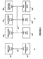
- a digital device 102 may be coupled to one or more peripheral devices 104 by a single-node data, address and control bus 106 adapted for a serial clock, and data and control input-output (hereinafter "SCIO").
- the digital device 102 may be a digital processor, e.g ., microprocessor, a microcontroller, a digital signal processor (DSP), a programmable logic array (PLA), an application specific integrated circuit (ASIC) and the like.
- the peripheral device 104 may be serial non-volatile memory, e.g ., one time programmable (OTP) memory, electrically programmable read only memory (EPROM), electrically erasable and programmable read only memory (EEPROM), FLASH memory and the like.
- the peripheral device 104 may also be serial access volatile memory, e.g ., static random access memory (SRAM), dynamic random access memory (DRAM) and the like.
- the peripheral device 104 may also be a sensor or other type of peripheral, e.g ., video camera, analog-to-digital converter (ADC), digital-to-analog converter (DAC), digital potentiometer, programmable gain amplifier, input-output (I/O) port expander, process sensor, for example but not limited to, temperature, pressure, vibration, flow rate, pH, etc.
- ADC analog-to-digital converter
- DAC digital-to-analog converter
- I/O input-output
- process sensor for example but not limited to, temperature, pressure, vibration, flow rate, pH, etc.
- the single-node data, address and control bus 106 may be a conductive node, e.g ., printed circuit board conductor, integrated circuit die bond node and the like.
- the digital device 102 and/or the peripheral device 104 may have, for example but not limited to, an active pull-up (e.g ., logic '1'), pull-down (e.g ., logic '0') and high impedance third state (tri-state) driver coupled to the single-node data, address and control bus 106.
- An open collector configuration with a pull-up resistor is also contemplated herein and within the scope of this disclosure.
- the digital device 102 and the peripheral device 104 may be coupled to a common power supply return, e.g ., V SS , ground, etc ., and power, e.g ., V CC ), V DD , etc.
- one digital device 102 may be defined as the master, and is responsible for initiating and coordinating all operations with each peripheral (slave) device 104 on the bus 106. Each peripheral device 104 responds to actions initiated by the master digital device 102.
- the peripheral device 104 may be designed for any number of purposes.
- Data may be transferred between the master device and a selected slave device with serial digital binary signals over the bus 106
- the signal protocol on the bus 106 may be, for example but not limited to, Manchester-encoding, or any other type of serial signal protocol, e.g., non-return to zero (NRZ), pulse position modulation (PPM), frequency shift keying (FSK), phase shift keying (PSK), amplitude shift keying (ASK) and the like, that may use an initial Start header byte (or other length word) to synchronize the master and slave clocks together.
- NRF non-return to zero
- PPM pulse position modulation
- FSK frequency shift keying
- PSK phase shift keying
- ASK amplitude shift keying
- Single-node data, address and control over the bus 106 is controlled by the master digital device 102 which determines the clock period, controls bus access and initiates all operations, while the peripheral device(s) 104 act as slaves. Both master and slave devices may operate as a transmitter or a receiver, but the master device determines which mode and operation is active.
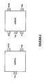
- a peripheral device 104 may be packaged in a low pin count integrated circuit package, e.g ., SOT23-3, SOT23-5, SC70-3 and the like. It is contemplated and within the scope of this disclosure that any low pin count integrated circuit package may be used to enclose the peripheral device 104.
- the integrated circuit package may have a ground terminal, V SS ; a power terminal, V DD or V CC ; and a bidirectional serial input-output (I/O) terminal adapted for receiving and transmitting the SCIO.
- hardwired address selection terminals for example but not limited to, A0 and A1 may be used when more then three terminals are available on the integrated circuit package. It is contemplated and within the scope of this disclosure that block address set-up may be performed via software instructions through the SCIO terminal over the single-node data, address and control bus 106. It is also contemplated and within the scope of the present disclosure that a digital device 102 and/or the peripheral device 104 may be packaged in a dual die integrated circuit package wherein the single-node data, address and control bus 106 may be a bond wire (not shown) or other direct die-to-die connection within the integrated circuit package.
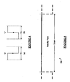
- a standby pulse 320 precedes sending a start header 322 by the master device.
- An acknowledge sequence 324 follows after the start header 322 has been sent.
- the acknowledge sequence 324 comprises a master acknowledge (MAK) followed by no slave acknowledge (NoSAK) (see Figure 9 ).
- a device address 326 is sent by the master device followed by an acknowledge (ACK) 328a sequence (see Figure 9 ).
- a command 330 is sent by the master device followed by another ACK 328a sequence.
- Word address and/or data (information) bytes 332 may thereafter be sent by the either the master and/or slave devices if required, e.g ., memory write to or data retrieval from a slave peripheral device 104.
- the ACK 328a sequence occurs after each information byte is sent until the last information byte is sent, then an ACK 328b sequence (see Figure 9 ) is sent which indicates completion of the information byte(s) transfer(s).
- FIG. 4 depicted are schematic timing diagrams of Manchester encoding of serial digital signals over the single-node data, address and control bus of Figure 1 .
- the single-node data, address and control bus 106 may operate as a bidirectional single-node bus and data transmission protocol.
- a device that sends data onto the bus 106 may be defined as a transmitter, and a device receiving data as a receiver.
- the bus 106 is controlled by the master, and the master determines a clock period, control bus access and may initiate all operations between the master and slave devices.
- the digital device 102 will be the master and the peripheral device 104 will be the slave. Both master and slave may operate as transmitter or receiver, but the master determines which operational mode (transmit or receive) is activated for each device. Multiple devices may be connected to the bus 106, though only one will serve as the master.
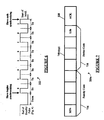
- the transmitter will change the voltage levels of SCIO on the single-node bus 106 during a bit period, T E , preferably at substantially the middle of the bit period, T E .
- the SCIO on the bus 106 is the only I/O signal required since both the serial clock and data are embedded together through Manchester encoding.
- each bit consists of a mandatory edge in substantially the middle of the bit period, T E .
- the direction of this edge determines the logic value of the bit. A rising edge indicates a logic "1" and a failing edge indicates a logic "0.”
- Examples for Manchester encoding are: (a) for a logic "0" the single-node bus voltage level will go from a high, e.g ., Vdd, to a low, e.g ., Vss (falling edge), and (b) for a logic "1" the single-node bus voltage level will go from a low, e.g., Vss, to a high, e.g ., Vdd (rising edge).
- the receiver will sense the single-node bus voltage level changes and thereby decode the rising and falling edges of the SCIO data stream into logic 1s and logic 0s, respectively, and will also synchronize its internal clock with the bit period, T E ., of the transmitter.
- the standby pulse 320 is generated by the bus 106 being driven by the master device to a logic high (1) pulse having a time duration of TSTBY, e.g ., 600 microseconds minimum.
- the standby pulse 320 indicates a reset condition to all devices connected to the bus 106, and puts these devices in a standby mode, ready for reception of a new command beginning with the start header 322.
- the standby pulse 320 is used when selecting a new slave device.
- the standby pulse 320 may also be used to prematurely terminate a command.
- the start header 322 begins when a logic level low (0) pulse is asserted by the device master on the bus 106.
- the logic level 0 pulse on the bus 106 remains low for a time duration of THDR, e.g ., about 5 microseconds.
- the time duration, THDR allows for device oscillator start-up, etc ., thereafter the start header 322 may consist of, for example but not limited to, an 8-bit binary code ( e.g , 01010101) being generated from the transmitting device.
- the slave device begins synchronization (e.g ., internal clock timing synchronization) until the last transition (after 01010101 is generated) where the slave device ends synchronization.
- the start header 322 is always the first byte transmitted for any given command. After the bits ( e.g ., byte) of the start header 322 have been sent, an acknowledge sequence is performed. Just for this specific sequence, only the MAK is asserted and there is no SAK (slave acknowledge), e.g ., a "NoSAK" occurring after the eight transmitted bits of the start header 322 have completed. See description of Figure 9 below.
- FIGS. 7 and 8 depicted are schematic diagrams of an 8-bit device addressing structure and a 12-bit device addressing structure, respectively, for the enhanced single-node protocol shown in Figure 3 .
- the device address 326 is sent.
- the device address 326 may consist of either one or two bytes depending on whether 8-bit ( Figure 7 ) or 12 -bit ( Figure 8 ) device addressing is supported, respectively.
- the purpose of the device address 326 is to select a specific slave device connected on the bus 106. Therefore, every slave device connected to the bus 106 must have a unique device address 326, otherwise bus conflicts will occur and operation will be undefined. All ones in the 12-bit select 834 indicates 12-bit addressing of the device.
- the family codes 736 and 836 are 4-bit values included in the device addresses 326a and 326b, respectively, and indicate the family in which the peripheral devices 104 reside.
- peripheral device families include, but are not limited to, memory devices, temperature sensors, programmable gain amplifiers, I/O port expanders, analog-to-digital converters (ADC) and digital-to-analog converters (DAC).
- the device codes 738 and 838 are 4-bit and 8-bit values, respectively, depending on whether 8-bit ( Figure 7 ) or 12 -bit ( Figure 8 ) device addressing is supported.
- the device codes 738 and 838 are used to differentiate devices with the same family codes. It is contemplated and with the scope of this disclosure that some devices may support programmable device codes bits 740 and 840, whereas on other devices these bits may be fixed at the time of manufacture of the device.
- the 4-bit device code 738 allows up to 16 devices from the same family on the bus 106.
- the 8-bit device code 838 allows up to 256 devices from the same family on the bus 106.
- FIG. 9 depicted are schematic timing diagrams of master and slave acknowledge sequences for the enhanced single-node protocol shown in Figure 3 .
- the acknowledge sequence, ACK 324, of Figure 3 is comprised of two bit periods, T E , the first bit period is for the MAK, at logic 1, and the second bit period is for NoSAK, NoSak appears as no edge at all, e.g ., no device transmitting, a non-asserted state (tri-state output drive).
- the acknowledge sequence, ACK 324 is used to indicate completion of the start header 322 and completion of the first byte of a 12-bit device address (see Figure 8 ).
- the acknowledge sequence, ACK 328a, of Figure 3 is comprised of two bits, the first bit is for MAK, logic 1, and the second bit is for SAK, always a logic 1.
- the acknowledge sequence, ACK 328a is used to indicate continuation of an operation, as well as to confirm reception of a byte.
- the acknowledge sequence, ACK 328b, of Figure 3 is comprised of two bits, the first bit is for NoMAK, logic 0, and the second bit is for SAK, always a logic 1.
- the acknowledge sequence, ACK 328b, is used to indicate termination of an operation, as well as to confirm reception of a byte.
- the MAK or NoMAK bit occurs as the first bit of every acknowledge sequence, ACK 324 and ACK 328. It is always sent by the master device, regardless of which device (master or slave) transmitted the preceding byte. A MAK is sent as a logic "1" and a NoMAK as a logic "0.” Sending a MAK during the acknowledge sequence, ACK 328a, indicates that the current operation is to be continued. This means that more data is to be sent by the device acting as transmitter. A NoMAK indicates that the current operation is to be terminated immediately following completion of the acknowledge sequence, ACK 328b.
- the SAK bit occurs as the second bit of the acknowledge sequence, ACK 328, and is sent strictly by the slave device regardless of which device transmitted the preceding byte.
- the SAK bit is sent as a logic "1" and the absence of a SAK bit (NoSAK) appears as no edge at all, i.e., no device transmitting. If after sending a device address 326, no SAK bit is received from the addressed slave device, then an error may have occurred. When an absence of a SAK bit occurs the master device may perform a standby pulse 320 and then may begin the desired command again.
- a non-occurrence of a SAK bit may also be used for determining the slave devices that are connected to the bus 106 ( Figure 1 ).
- the bus master 102 may send out a plurality of interrogation commands, each one of the plurality of interrogation commands has a unique address associated therewith. If a SAK bit is received after the interrogation command, then there is a slave device 104 connected to the bus 106 having the address of that interrogation command. However, if there is an absence of a SAK bit (NoSAK) then there is no slave device 104 connected to the bus 106 having the address of the interrogation command resulting in the NoSAK.
- NoSAK absence of a SAK bit
- FIG. 10 depicted is a schematic timing diagram of a hold pulse, master acknowledge and slave acknowledge for the enhanced single-node protocol shown in Figure 3 .
- the hold pulse 1050 is optional and suspends operation of the currently addressed slave device when asserted.
- the hold pulse 1050 allows the master device to service interrupts, etc.
- the master device brings SCIO to a logic low (0) on the bus 106 at the beginning of the next MAK bit period and continues to keep SCIO low while in hold, for a minimum of one bit period, TE. This will initiate a hold on the addressed slave device.
- the hold pulse 1050 is released (SCIO back to a logic high (1)) and then within the appropriate bit periods, T E , first a MAK and then a SAK, will be asserted. Thereafter normal data/address transmission resumes.
- the hold pulse 1050 cannot occur during a start header 322.
- Figure 11 illustrates a schematic diagram of a multi-byte read sequence for the enhanced single-node protocol shown in Figure 3 .
- an acknowledge sequence is sent.
- a MAK and SAK sequence occur.
- no further data byte is desired to be sent (read) from the slave device, a NoMAK and SAK sequence occur.
- the NoMAK response from the master device ends the transmission of data from the device slave to the master device.
- Figure 12 illustrates a schematic diagram of a multi-byte write sequence for the enhanced single-node protocol shown in Figure 3 .
- an acknowledge sequence is sent.
- a MAK and SAK sequence occur.
- no further data byte is to be written to the slave device, a NoMAK and SAK sequence occur.
- the NoMAK response from the master device ends the transmission of data from the master device to the slave device.
- read and/or write sequences may also comprise error checking parity bits, and/or error checking and correcting bits.
- Slave devices have a standby mode during which time the slave device is waiting to begin a new command.
- the standby mode will be entered upon the following conditions: (a) A NoMAK followed by a SAK (i.e., valid termination of a command), or (b) reception of a standby pulse 320.
- a high-to-low transition of the SCIO will cause the slave device(s) to exit standby and prepare the device for reception of the start header 322.
- the standby mode may also be used to provide a low-power mode of operation by only activating the slave device(s) at the beginning of the first low pulse of the start header 322.
- Slave devices have a device idle mode during which all serial data is ignored until a standby pulse 320 occurs.
- the idle mode will be entered upon the following conditions: (a) invalid device address, (b) invalid command byte, and/or (c) missed edge transition, except when the slave device enters the standby mode, as described hereinabove.
Landscapes
- Engineering & Computer Science (AREA)
- Theoretical Computer Science (AREA)
- Physics & Mathematics (AREA)
- General Engineering & Computer Science (AREA)
- General Physics & Mathematics (AREA)
- Information Transfer Systems (AREA)
- Communication Control (AREA)
Description
- The present disclosure relates generally to communications between semiconductor devices, e.g., processors, memory, peripherals, sensors, etc., and, more particularly, to semiconductor devices using enhanced single-node protocols for data, address and control operations.
- Integrated circuit digital devices, e.g., digital processors such as, for example but not limited to, microprocessors, microcontrollers, digital signal processors (DSP), programmable logic array (PLA), application specific integrated circuit (ASIC) and the like, are becoming smaller and with fewer external input-output (I/O) signal connections (e.g., pins or leads) for both cost and space considerations. Typically an integrated circuit device may be in an integrated circuit package having a plurality of external connections. At least two of these external connections must be used for power and ground, e.g., VDD and VSS, respectively. The remaining few external connections are left for I/O signals. For example, the Serial Peripheral Interface (SPI) Bus requires four external signal connections, the Universal Serial Bus (USB) requires two external signal connections and also may require two external power connections, the Inter-Integrated Circuit (I2C) requires two external signal connections, and The Controller Area Network (CAN) may use a two wire twisted pair bus.
- The integrated circuit devices may benefit from additional device functions, e.g., external memory, high speed interfaces, sensors, peripherals, etc. Memory may be, for example but not limited to, one time programmable (OTP), electrically programmable read only memory (EPROM), electrically erasable and programmable read only memory (EEPROM), FLASH memory, static random access memory (SRAM), dynamic random access memory (DRAM), etc. High speed interfaces may be, for example but not limited to, Ethernet, Universal Serial Bus (USB), Firewire, and the like. Sensors may be used to measure, for example but not limited to, pressure, temperature, humidity, voltage, current, frequency, time, radiation, pH, etc. Peripherals may be used to capture, for example but not limited to, video, audio, radar, infrared, ultrasonic information, etc. Integrated circuit package size for these devices is being more critical from both cost and printed circuit board space requirements.
- US Patent Application
US2004/0208200 discloses a single wire communication bus for miniature low-power systems with a predetermined addressing scheme. - Therefore what is needed is a robust more flexible data, address and control protocol for communicating between the integrated circuit devices and additional external device functions, wherein this protocol requires a minimum number of signal I/O connections between each connected package. This and other objects can be achieved by an enhanced single-node protocol and a system using such a protocol as defined in the independent claims. Further enhancements are characterized in the dependent claims.
- A single-node signal connection may be used to electrically couple the integrated circuit device and any additional device functions together so that the robust data, address and control protocol may be effectively utilized, according to the teachings of this disclosure.
- For example, additional external devices (hereinafter "peripherals") may be coupled to an integrated circuit device with a minimum number of connections, e.g., a single-node bus for data, address and control, plus power and ground, e.g., VDD (or VCC) and VSS, respectively, may be required for operation of the integrated circuit device and peripheral(s), thus a minimum of three external connections (pin, surface mount lead, etc.) of an integrated circuit package, e.g., SOT 23-3, SC70-3, etc., may be used for packaging the integrated circuit device and/or peripheral. Peripheral address selection when implementing a plurality of peripherals may utilize specifically defined device type addressing and/or additional address select connections on a low pin count integrated circuit package, e.g., SOT 23-5, SOT 23-6, MSOP-8, SOIC-8 and the like, and/or by programming a peripheral address for each of the peripherals via the single-node data, address and control bus.
- According to a specific example embodiment as described in the present disclosure, an enhanced single-node protocol for data, address and control operations between digital devices may comprise the steps of: providing a master device having a bidirectional serial clock, and data and control input-output (SCIO) terminal; providing at least one slave device having a bidirectional SCIO terminal, wherein the master device SCIO terminal and the at least one slave device SCIO terminal are coupled together; generating a standby pulse from the master device SCIO terminal; generating a start header from the master device SCIO terminal; generating a master acknowledge from the master device SCIO terminal; generating a device address from the master device SCIO terminal; generating the master acknowledge from master device SCIO terminal; generating a slave acknowledge from the slave device SCIO terminal; generating a command from the master device SCIO terminal; generating the master acknowledge from the master device SCIO terminal; generating the slave acknowledge from the slave device SCIO terminal; generating an information byte from the master device SCIO terminal when sending information to the slave device SCIO terminal; generating an information byte from the slave device SCIO terminal when sending information to the master device SCIO terminal; generating a termination master acknowledge from the master device SCIO terminal; and generating the slave acknowledge from the slave device SCIO terminal.
- According to another specific example embodiment as described in the present disclosure, an enhanced single-node protocol for data, address and control operations between digital devices, said protocol comprising the steps of: (a) providing a master device having a bidirectional serial clock, and data and control input-output (SCIO) terminal; (b) providing at least one slave device having a bidirectional SCIO terminal, wherein the master device SCIO terminal and the at least one slave device SCIO terminal are coupled together; (c) generating a standby pulse from the master device SCIO terminal; (d) generating a start header from the master device SCIO terminal; (e) generating a master acknowledge from the master device SCIO terminal; (f) generating a one of a plurality of device addresses from the master device SCIO terminal; (g) generating the master acknowledge from master device SCIO terminal; (h) determining whether a slave acknowledge is generated for the one of the plurality of device addresses, wherein if the slave acknowledge is generated then storing the one of the plurality of device addresses in a slave device table; and (i) repeating steps (c) through (h) until every one of the plurality of device addresses have been generated.
- A more complete understanding of the present disclosure thereof may be acquired by referring to the following description taken in conjunction with the accompanying drawing, wherein:
-
Figure 1 illustrates a schematic block diagram of an integrated circuit digital device coupled to a peripheral device with a single-node data, address and control bus, according to a specific example embodiment of this disclosure; -
Figure 2 illustrates schematic plan view diagrams of example low pin count integrated circuit packages, according to a specific example embodiment of this disclosure; -
Figure 3 illustrates a schematic diagram of a command structure for an enhanced single-node protocol for data, address and control operations, according to a specific example embodiment of this disclosure; -
Figure 4 illustrates schematic timing diagrams of Manchester encoding of serial digital signals over the single-node data, address and control bus ofFigure 1 ; -
Figure 5 illustrates a schematic timing diagram of a standby pulse for the enhanced single-node protocol shown inFigure 3 ; -
Figure 6 illustrates a schematic timing diagram of a start header for the enhanced single-node protocol shown inFigure 3 ; -
Figure 7 illustrates a schematic diagram of an 8-bit device addressing structure for the enhanced single-node protocol shown inFigure 3 ; -
Figure 8 illustrates a schematic diagram of a 12-bit device addressing structure for the enhanced single-node protocol shown inFigure 3 ; -
Figure 9 illustrates schematic timing diagrams of master and slave acknowledge sequences for the enhanced single-node protocol shown inFigure 3 ; -
Figure 10 illustrates a schematic timing diagram of a hold pulse, master acknowledge and slave acknowledge for the enhanced single-node protocol shown inFigure 3 ; -
Figure 11 illustrates a schematic diagram of a multi-byte read sequence for the enhanced single-node protocol shown inFigure 3 ; and -
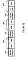
Figure 12 illustrates a schematic diagram of a multi-byte write sequence for the enhanced single-node protocol shown inFigure 3 . - While the present disclosure is susceptible to various modifications and alternative forms, specific example embodiments thereof have been shown in the drawings and are herein described in detail. It should be understood, however, that the description herein of specific example embodiments is not intended to limit the disclosure to the particular forms disclosed herein, but on the contrary, this disclosure is to cover all modifications and equivalents as defined by the appended claims.
- Referring now to the drawing, the details of specific example embodiments are schematically illustrated. Like elements in the drawings will be represented by like numbers, and similar elements will be represented by like numbers with a different lower case letter suffix.
- Referring now to
Figure 1 , depicted is a schematic block diagram of an digital device coupled to a peripheral device with a single-node data, address and control bus, according to a specific example embodiment of this disclosure. Adigital device 102 may be coupled to one or moreperipheral devices 104 by a single-node data, address andcontrol bus 106 adapted for a serial clock, and data and control input-output (hereinafter "SCIO"). Thedigital device 102 may be a digital processor, e.g., microprocessor, a microcontroller, a digital signal processor (DSP), a programmable logic array (PLA), an application specific integrated circuit (ASIC) and the like. - The
peripheral device 104 may be serial non-volatile memory, e.g., one time programmable (OTP) memory, electrically programmable read only memory (EPROM), electrically erasable and programmable read only memory (EEPROM), FLASH memory and the like. Theperipheral device 104 may also be serial access volatile memory, e.g., static random access memory (SRAM), dynamic random access memory (DRAM) and the like. Theperipheral device 104 may also be a sensor or other type of peripheral, e.g., video camera, analog-to-digital converter (ADC), digital-to-analog converter (DAC), digital potentiometer, programmable gain amplifier, input-output (I/O) port expander, process sensor, for example but not limited to, temperature, pressure, vibration, flow rate, pH, etc. The single-node data, address andcontrol bus 106 may be a conductive node, e.g., printed circuit board conductor, integrated circuit die bond node and the like. - The
digital device 102 and/or theperipheral device 104 may have, for example but not limited to, an active pull-up (e.g., logic '1'), pull-down (e.g., logic '0') and high impedance third state (tri-state) driver coupled to the single-node data, address andcontrol bus 106. An open collector configuration with a pull-up resistor is also contemplated herein and within the scope of this disclosure. Thedigital device 102 and theperipheral device 104 may be coupled to a common power supply return, e.g., VSS, ground, etc., and power, e.g., VCC), VDD, etc. - Communications through a single I/O signal between multiple devices over a single node "bussed" system is contemplated herein. According to the teachings of this disclosure, one
digital device 102 may be defined as the master, and is responsible for initiating and coordinating all operations with each peripheral (slave)device 104 on thebus 106. Eachperipheral device 104 responds to actions initiated by the masterdigital device 102. Theperipheral device 104 may be designed for any number of purposes. - Data may be transferred between the master device and a selected slave device with serial digital binary signals over the
bus 106 The signal protocol on thebus 106 may be, for example but not limited to, Manchester-encoding, or any other type of serial signal protocol, e.g., non-return to zero (NRZ), pulse position modulation (PPM), frequency shift keying (FSK), phase shift keying (PSK), amplitude shift keying (ASK) and the like, that may use an initial Start header byte (or other length word) to synchronize the master and slave clocks together. - Single-node data, address and control over the
bus 106 is controlled by the masterdigital device 102 which determines the clock period, controls bus access and initiates all operations, while the peripheral device(s) 104 act as slaves. Both master and slave devices may operate as a transmitter or a receiver, but the master device determines which mode and operation is active. - Referring to
Figure 2 , depicted are schematic plan view diagrams of example low pin count integrated circuit packages, according to a specific example embodiment of this disclosure. Aperipheral device 104 may be packaged in a low pin count integrated circuit package, e.g., SOT23-3, SOT23-5, SC70-3 and the like. It is contemplated and within the scope of this disclosure that any low pin count integrated circuit package may be used to enclose theperipheral device 104. The integrated circuit package may have a ground terminal, VSS; a power terminal, VDD or VCC; and a bidirectional serial input-output (I/O) terminal adapted for receiving and transmitting the SCIO. - In addition, hardwired address selection terminals, for example but not limited to, A0 and A1 may be used when more then three terminals are available on the integrated circuit package. It is contemplated and within the scope of this disclosure that block address set-up may be performed via software instructions through the SCIO terminal over the single-node data, address and
control bus 106. It is also contemplated and within the scope of the present disclosure that adigital device 102 and/or theperipheral device 104 may be packaged in a dual die integrated circuit package wherein the single-node data, address andcontrol bus 106 may be a bond wire (not shown) or other direct die-to-die connection within the integrated circuit package. - Referring to
Figure 3 , depicted is a schematic diagram of a command structure for an enhanced single-node protocol for data, address and control operations, according to a specific example embodiment of this disclosure. Astandby pulse 320 precedes sending astart header 322 by the master device. An acknowledgesequence 324 follows after thestart header 322 has been sent. The acknowledgesequence 324 comprises a master acknowledge (MAK) followed by no slave acknowledge (NoSAK) (seeFigure 9 ). Next adevice address 326 is sent by the master device followed by an acknowledge (ACK) 328a sequence (seeFigure 9 ). Acommand 330 is sent by the master device followed by anotherACK 328a sequence. Word address and/or data (information) bytes 332 may thereafter be sent by the either the master and/or slave devices if required, e.g., memory write to or data retrieval from a slaveperipheral device 104. TheACK 328a sequence occurs after each information byte is sent until the last information byte is sent, then anACK 328b sequence (seeFigure 9 ) is sent which indicates completion of the information byte(s) transfer(s). - Referring to
Figure 4 , depicted are schematic timing diagrams of Manchester encoding of serial digital signals over the single-node data, address and control bus ofFigure 1 . The single-node data, address andcontrol bus 106 may operate as a bidirectional single-node bus and data transmission protocol. - A device that sends data onto the
bus 106 may be defined as a transmitter, and a device receiving data as a receiver. Thebus 106 is controlled by the master, and the master determines a clock period, control bus access and may initiate all operations between the master and slave devices. Typically, thedigital device 102 will be the master and theperipheral device 104 will be the slave. Both master and slave may operate as transmitter or receiver, but the master determines which operational mode (transmit or receive) is activated for each device. Multiple devices may be connected to thebus 106, though only one will serve as the master. - The transmitter will change the voltage levels of SCIO on the single-
node bus 106 during a bit period, TE, preferably at substantially the middle of the bit period, TE. The SCIO on thebus 106 is the only I/O signal required since both the serial clock and data are embedded together through Manchester encoding. In Manchester encoding, each bit consists of a mandatory edge in substantially the middle of the bit period, TE. The direction of this edge determines the logic value of the bit. A rising edge indicates a logic "1" and a failing edge indicates a logic "0." - Examples for Manchester encoding are: (a) for a logic "0" the single-node bus voltage level will go from a high, e.g., Vdd, to a low, e.g., Vss (falling edge), and (b) for a logic "1" the single-node bus voltage level will go from a low, e.g., Vss, to a high, e.g., Vdd (rising edge). The receiver will sense the single-node bus voltage level changes and thereby decode the rising and falling edges of the SCIO data stream into logic 1s and logic 0s, respectively, and will also synchronize its internal clock with the bit period, TE., of the transmitter.
- Referring to
Figure 5 , depicted is a schematic timing diagram of a standby pulse for the enhanced single-node protocol shown inFigure 3 . Thestandby pulse 320 is generated by thebus 106 being driven by the master device to a logic high (1) pulse having a time duration of TSTBY, e.g., 600 microseconds minimum. Thestandby pulse 320 indicates a reset condition to all devices connected to thebus 106, and puts these devices in a standby mode, ready for reception of a new command beginning with thestart header 322. Thestandby pulse 320 is used when selecting a new slave device. Thestandby pulse 320 may also be used to prematurely terminate a command. - Referring to
Figure 6 , depicted is a schematic timing diagram of a start header for the enhanced single-node protocol shown inFigure 3 . Thestart header 322 begins when a logic level low (0) pulse is asserted by the device master on thebus 106. Thelogic level 0 pulse on thebus 106 remains low for a time duration of THDR, e.g., about 5 microseconds. The time duration, THDR, allows for device oscillator start-up, etc., thereafter thestart header 322 may consist of, for example but not limited to, an 8-bit binary code (e.g, 01010101) being generated from the transmitting device. At thefirst bus 106 level transition to alogic 1, the slave device begins synchronization (e.g., internal clock timing synchronization) until the last transition (after 01010101 is generated) where the slave device ends synchronization. Thestart header 322 is always the first byte transmitted for any given command. After the bits (e.g., byte) of thestart header 322 have been sent, an acknowledge sequence is performed. Just for this specific sequence, only the MAK is asserted and there is no SAK (slave acknowledge), e.g., a "NoSAK" occurring after the eight transmitted bits of thestart header 322 have completed. See description ofFigure 9 below. - Referring to
Figures 7 and8 , depicted are schematic diagrams of an 8-bit device addressing structure and a 12-bit device addressing structure, respectively, for the enhanced single-node protocol shown inFigure 3 . Following thestart header 322, thedevice address 326 is sent. Thedevice address 326 may consist of either one or two bytes depending on whether 8-bit (Figure 7 ) or12 -bit (Figure 8 ) device addressing is supported, respectively. The purpose of thedevice address 326 is to select a specific slave device connected on thebus 106. Therefore, every slave device connected to thebus 106 must have aunique device address 326, otherwise bus conflicts will occur and operation will be undefined. All ones in the 12-bit select 834 indicates 12-bit addressing of the device. - The
family codes peripheral devices 104 reside. Examples of peripheral device families include, but are not limited to, memory devices, temperature sensors, programmable gain amplifiers, I/O port expanders, analog-to-digital converters (ADC) and digital-to-analog converters (DAC). - The
device codes Figure 7 ) or12 -bit (Figure 8 ) device addressing is supported. Thedevice codes device codes bits bit device code 738 allows up to 16 devices from the same family on thebus 106. The 8-bit device code 838 allows up to 256 devices from the same family on thebus 106. - Referring to
Figure 9 , depicted are schematic timing diagrams of master and slave acknowledge sequences for the enhanced single-node protocol shown inFigure 3 . - The acknowledge sequence,
ACK 324, ofFigure 3 is comprised of two bit periods, TE, the first bit period is for the MAK, atlogic 1, and the second bit period is for NoSAK, NoSak appears as no edge at all, e.g., no device transmitting, a non-asserted state (tri-state output drive). The acknowledge sequence,ACK 324, is used to indicate completion of thestart header 322 and completion of the first byte of a 12-bit device address (seeFigure 8 ). - The acknowledge sequence,
ACK 328a, ofFigure 3 is comprised of two bits, the first bit is for MAK,logic 1, and the second bit is for SAK, always alogic 1. The acknowledge sequence,ACK 328a, is used to indicate continuation of an operation, as well as to confirm reception of a byte. - The acknowledge sequence,
ACK 328b, ofFigure 3 is comprised of two bits, the first bit is for NoMAK,logic 0, and the second bit is for SAK, always alogic 1. The acknowledge sequence,ACK 328b, is used to indicate termination of an operation, as well as to confirm reception of a byte. - However no slave device will respond with a SAK until a specific slave device has been selected. This is required in order to avoid possible bus collision due to multiple slave devices transmitting at the same time. Referring back to
Figure 7 , for 8-bit addressing, there will be no SAK occurring after thestart header 322 only. Referring back toFigure 8 , for 12-bit addressing, there will be no SAKs occurring after both thestart header 322 and the most significant byte (MSB) 834+836 of thedevice address 326b. - The MAK or NoMAK bit occurs as the first bit of every acknowledge sequence,
ACK 324 andACK 328. It is always sent by the master device, regardless of which device (master or slave) transmitted the preceding byte. A MAK is sent as a logic "1" and a NoMAK as a logic "0." Sending a MAK during the acknowledge sequence,ACK 328a, indicates that the current operation is to be continued. This means that more data is to be sent by the device acting as transmitter. A NoMAK indicates that the current operation is to be terminated immediately following completion of the acknowledge sequence,ACK 328b. - The SAK bit occurs as the second bit of the acknowledge sequence,
ACK 328, and is sent strictly by the slave device regardless of which device transmitted the preceding byte. The SAK bit is sent as a logic "1" and the absence of a SAK bit (NoSAK) appears as no edge at all, i.e., no device transmitting. If after sending adevice address 326, no SAK bit is received from the addressed slave device, then an error may have occurred. When an absence of a SAK bit occurs the master device may perform astandby pulse 320 and then may begin the desired command again. - A non-occurrence of a SAK bit may also be used for determining the slave devices that are connected to the bus 106 (
Figure 1 ). Thebus master 102 may send out a plurality of interrogation commands, each one of the plurality of interrogation commands has a unique address associated therewith. If a SAK bit is received after the interrogation command, then there is aslave device 104 connected to thebus 106 having the address of that interrogation command. However, if there is an absence of a SAK bit (NoSAK) then there is noslave device 104 connected to thebus 106 having the address of the interrogation command resulting in the NoSAK. - Referring to
Figure 10 , depicted is a schematic timing diagram of a hold pulse, master acknowledge and slave acknowledge for the enhanced single-node protocol shown inFigure 3 . Thehold pulse 1050 is optional and suspends operation of the currently addressed slave device when asserted. Thehold pulse 1050 allows the master device to service interrupts, etc. The master device brings SCIO to a logic low (0) on thebus 106 at the beginning of the next MAK bit period and continues to keep SCIO low while in hold, for a minimum of one bit period, TE. This will initiate a hold on the addressed slave device. To bring the most recently addressed slave device out of a hold condition, thehold pulse 1050 is released (SCIO back to a logic high (1)) and then within the appropriate bit periods, TE, first a MAK and then a SAK, will be asserted. Thereafter normal data/address transmission resumes. Thehold pulse 1050 cannot occur during astart header 322. -
Figure 11 illustrates a schematic diagram of a multi-byte read sequence for the enhanced single-node protocol shown inFigure 3 . After each data byte from the slave device an acknowledge sequence is sent. When another data byte is to be sent (read) from the slave device, a MAK and SAK sequence occur. When no further data byte is desired to be sent (read) from the slave device, a NoMAK and SAK sequence occur. The NoMAK response from the master device ends the transmission of data from the device slave to the master device. -
Figure 12 illustrates a schematic diagram of a multi-byte write sequence for the enhanced single-node protocol shown inFigure 3 . After each data byte to the slave device an acknowledge sequence is sent. When another data byte is to be written to the slave device, a MAK and SAK sequence occur. When no further data byte is to be written to the slave device, a NoMAK and SAK sequence occur. The NoMAK response from the master device ends the transmission of data from the master device to the slave device. - It is contemplated and within the scope of this disclosure that read and/or write sequences may also comprise error checking parity bits, and/or error checking and correcting bits.
- Slave devices have a standby mode during which time the slave device is waiting to begin a new command. The standby mode will be entered upon the following conditions: (a) A NoMAK followed by a SAK (i.e., valid termination of a command), or (b) reception of a
standby pulse 320. A high-to-low transition of the SCIO will cause the slave device(s) to exit standby and prepare the device for reception of thestart header 322. The standby mode may also be used to provide a low-power mode of operation by only activating the slave device(s) at the beginning of the first low pulse of thestart header 322. - Slave devices have a device idle mode during which all serial data is ignored until a
standby pulse 320 occurs. The idle mode will be entered upon the following conditions: (a) invalid device address, (b) invalid command byte, and/or (c) missed edge transition, except when the slave device enters the standby mode, as described hereinabove.
Claims (15)
- An enhanced single-node protocol for data, address and control operations between digital devices, said protocol comprising the steps of:providing a master device (102; 102a) having a bidirectional serial clock, and data and control input-output (SCIO) terminal;providing at least one slave device (104; 104a-e) having a bidirectional SCIO terminal, wherein the master device SCIO terminal and the at least one slave device SCIO terminal are coupled together;generating a pulse (320) having a predefined duration from the master device SCIO terminal;generating a start header (322) from the master device SCIO terminal;generating a first master acknowledge (324) from the master device SCIO terminal;generating a device address (326; 326a; 326b) from the master device SCIO terminal;generating the first master acknowledge (328a) from master device SCIO terminal;generating a slave acknowledge (328a) from the slave device SCIO terminal;generating a command (330) from the master device SCIO terminal;generating the first master acknowledge (328a) from the master device SCIO terminal;generating the slave acknowledge (328a) from the slave device SCIO terminal;generating an information byte (332) from the master device SCIO terminal when sending information to the slave device SCIO terminal and/or generating an information byte (332) from the slave device SCIO terminal when sending information to the master device SCIO terminal;generating a second master acknowledge (328b) different from said first master acknowledge (324; 328a) from the master device SCIO terminal; andgenerating the slave acknowledge (328b) from the slave device SCIO terminal.
- The enhanced single-node protocol according to claim 1, wherein the step of generating the information byte (332) further comprises the steps of generating a plurality of information bytes wherein the first master acknowledge (328a) and the slave acknowledge (328a) are generated between each of the plurality of information bytes until the second master acknowledge (328b) from the master device SCIO terminal and the slave acknowledge (328b) from the slave device SCIO terminal are generated.
- The enhanced single-node protocol according to claim 2, wherein the first master acknowledge (324; 328a) represents a first logic, the slave acknowledge (328a; 328b) represents the first logic, and the second master acknowledge (328b) represents a second logic.
- The enhanced single-node protocol according to claim 3, wherein the first logic is a logic 1 and the second logic is a logic 0 or the first logic is a logic 0 and the second logic is a logic 1.
- The enhanced single-node protocol according to one of the preceding claims, wherein the master and slave devices (102; 102a; 104; 104a-e)use a Manchester signal protocol or a serial transfer signal protocol selected from the group consisting of non-return to zero (NRZ), pulse position modulation (PPM), frequency shift keying (FSK), phase shift keying (PSK), and amplitude shift keying (ASK).
- The enhanced single-node protocol according to one of the preceding claims, wherein the standby pulse is at least 600 microseconds.
- The enhanced single-node protocol according to one of the preceding claims, wherein the start header (322) comprises at least eight (8) bits and optionally comprises an eight (8) bit pattern of 01010101.
- The enhanced single-node protocol according to one of the preceding claims, wherein the device address (326a; 326b) comprises a family code (736) and a device code (738) and wherein the family code (736) is optionally four (4) bits and the device code (738) is optionally four (4) bits or eight (8) bits.
- The enhanced single-node protocol according to claim 8, wherein the device address (326b) comprises two bytes,
a first byte of the device address (326b) comprises a select header (834) of four (4) bits having a bit pattern of 1111 and a family code (836) of four (4) bits; and
a second byte of the device address (326b) comprises a device code (838) of eight (8) bits. - The enhanced single-node protocol according to one of the preceding claims, wherein the command (330) comprises eight (8) bits.
- The enhanced single-node protocol according to one of the preceding claims, further comprising the step of generating a hold pulse (1050) from the master device SCIO terminal, wherein the hold pulse (1050) suspends operation of a currently addressed slave (104; 104a-e).
- The enhanced single-node protocol according to claim 11, wherein the currently addressed slave (104; 104a-e) comes out of a hold condition when the hold pulse (1050) from the master device SCIO terminal goes from a logic 0 to a logic 1, the master acknowledge is generated and the slave acknowledge is generated.
- The enhanced single-node protocol according to one of the preceding claims, wherein the master device SCIO terminal is a connection or connection pad on a master device integrated circuit which is enclosed in an integrated circuit package and wherein the slave device SCIO terminal is a connection or connection pad on a slave device integrated circuit which is enclosed in an integrated circuit package.
- The enhanced single-node protocol according to one of the preceding claims, wherein a transmission error can be detected by the master device (102; 102a) if no slave acknowledge has been generated.
- A system comprising a master device (102; 102a) and a slave device (104; 104a-e) coupled through a bidirectional serial clock, and data, and control input output (SCIO) single node bus using an enhanced single-node protocol for data, address and control operations, wherein said system for communication between the master and slave device (102; 102a; 104; 104a-e) is operable to:- generate a pulse (320) having a predefined duration from a master device SCIO terminal;- generate a start header (322) from the master device SCIO terminal;- generate a first master acknowledge (324) from the master device SCIO terminal;- generate a one of a plurality of device addresses (326) from the master device SCIO terminal;- generate the first master acknowledge (328a) from master device SCIO terminal;- generate a slave acknowledge (328a) from a slave device SCIO terminal;- generate a command (330) from the master device SCIO terminal;- generate the first master acknowledge (328a) from the master device SCIO terminal;- generate the slave acknowledge (328a) from the slave device SCIO terminal;- generate an information byte (332) from the master device SCIO terminal when sending information to the slave device SCIO terminal and/or generate an information byte (332) from the slave device SCIO terminal when sending information to the master device SCIO terminal;- generate a second master acknowledge (328b) different from said first master acknowledge from the master device SCIO terminal; and- to generate the slave acknowledge (328b) from the slave device SCIO terminal.
Applications Claiming Priority (2)
| Application Number | Priority Date | Filing Date | Title |
|---|---|---|---|
| US11/855,294 US7788430B2 (en) | 2007-09-14 | 2007-09-14 | Enhanced single-node protocol for data, address and control operations |
| PCT/US2008/075994 WO2009036153A1 (en) | 2007-09-14 | 2008-09-11 | Enhanced single-node protocol for data, address and control operations |
Publications (2)
| Publication Number | Publication Date |
|---|---|
| EP2188727A1 EP2188727A1 (en) | 2010-05-26 |
| EP2188727B1 true EP2188727B1 (en) | 2013-04-10 |
Family
ID=40044165
Family Applications (1)
| Application Number | Title | Priority Date | Filing Date |
|---|---|---|---|
| EP08799463.8A Active EP2188727B1 (en) | 2007-09-14 | 2008-09-11 | Enhanced single-node protocol for data, address and control operations |
Country Status (6)
| Country | Link |
|---|---|
| US (1) | US7788430B2 (en) |
| EP (1) | EP2188727B1 (en) |
| KR (1) | KR101513488B1 (en) |
| CN (1) | CN101802801B (en) |
| TW (1) | TWI465927B (en) |
| WO (1) | WO2009036153A1 (en) |
Families Citing this family (6)
| Publication number | Priority date | Publication date | Assignee | Title |
|---|---|---|---|---|
| US8291143B1 (en) * | 2009-02-11 | 2012-10-16 | Brocade Communication Systems, Inc. | Single line communication |
| CN102468901A (en) * | 2010-11-02 | 2012-05-23 | 凹凸电子(武汉)有限公司 | Method for transmitting data |
| EP2533022A1 (en) * | 2011-06-10 | 2012-12-12 | Hexagon Technology Center GmbH | Extremely precise synchronised measuring value recording |
| US8832341B2 (en) | 2011-09-27 | 2014-09-09 | International Business Machines Corporation | Dynamically determining a primary or slave assignment based on receiving a power signal from the cable at the port of a device |
| US9973431B2 (en) * | 2015-12-11 | 2018-05-15 | Qualcomm Incorporated | Single line PMIC-host low-level control interface |
| US11886366B2 (en) | 2022-02-22 | 2024-01-30 | Qualcomm Incorporated | One-wire bidirectional bus signaling with manchester encoding |
Family Cites Families (6)
| Publication number | Priority date | Publication date | Assignee | Title |
|---|---|---|---|---|
| CA2080210C (en) * | 1992-01-02 | 1998-10-27 | Nader Amini | Bidirectional data storage facility for bus interface unit |
| WO2003096036A1 (en) | 2002-05-08 | 2003-11-20 | Semtech Corporation | Single-wire communication bus for miniature low-power systems |
| TWI255406B (en) * | 2003-06-06 | 2006-05-21 | Mitac Int Corp | Method for data transmission in the master device and the slave device |
| TWI310499B (en) * | 2005-04-26 | 2009-06-01 | Sunplus Technology Co Ltd | Slave and master of serial peripheral interface, system thereof, and method thereof |
| US7376020B2 (en) * | 2005-12-13 | 2008-05-20 | Microchip Technology Incorporated | Memory using a single-node data, address and control bus |
| US7589652B2 (en) * | 2007-04-12 | 2009-09-15 | Microchip Technology Incorporated | Read and write interface communications protocol for digital-to-analog signal converter with non-volatile memory |
-
2007
- 2007-09-14 US US11/855,294 patent/US7788430B2/en active Active
-
2008
- 2008-09-11 TW TW097134896A patent/TWI465927B/en active
- 2008-09-11 WO PCT/US2008/075994 patent/WO2009036153A1/en not_active Ceased
- 2008-09-11 EP EP08799463.8A patent/EP2188727B1/en active Active
- 2008-09-11 KR KR1020107006494A patent/KR101513488B1/en active Active
- 2008-09-11 CN CN2008801068184A patent/CN101802801B/en active Active
Also Published As
| Publication number | Publication date |
|---|---|
| US7788430B2 (en) | 2010-08-31 |
| KR101513488B1 (en) | 2015-04-20 |
| WO2009036153A1 (en) | 2009-03-19 |
| EP2188727A1 (en) | 2010-05-26 |
| KR20100058596A (en) | 2010-06-03 |
| CN101802801B (en) | 2013-02-06 |
| CN101802801A (en) | 2010-08-11 |
| TWI465927B (en) | 2014-12-21 |
| TW200928768A (en) | 2009-07-01 |
| US20090077193A1 (en) | 2009-03-19 |
Similar Documents
| Publication | Publication Date | Title |
|---|---|---|
| CN102047615B (en) | Serial-peripheral interface with reduced number of connection lines | |
| EP0419112A2 (en) | Serial data transmission | |
| US5974475A (en) | Method for flexible multiple access on a serial bus by a plurality of boards | |
| US7788430B2 (en) | Enhanced single-node protocol for data, address and control operations | |
| CN100440187C (en) | Method and data structure for random access via a bus connection | |
| US7209995B2 (en) | Efficient connection between modules of removable electronic circuit cards | |
| EP2278482A2 (en) | Multiple removable non-volatile memory cards serially communicating with a host | |
| US20100064083A1 (en) | Communications device without passive pullup components | |
| US11556492B1 (en) | Synchronous serial interface allowing communication with multiple peripheral devices using a single chip select | |
| US7430259B2 (en) | Two-wire chip-to-chip interface | |
| WO2012036751A2 (en) | Different types of memory integrated in one chip by using a novel protocol | |
| WO2007124304A2 (en) | Serial communications bus with active pullup | |
| WO2000002134A2 (en) | Improved inter-device serial bus protocol | |
| WO2005106689A1 (en) | Bus system for selectively controlling a plurality of identical slave circuits connected to the bus and method therefore | |
| US20040095952A1 (en) | Method and system for a three conductor transceiver bus | |
| KR100973185B1 (en) | Memory using a single node's data, address, and control buses and digital systems using them | |
| CN115048330A (en) | Communication over I2C bus | |
| CN113886298B (en) | Electronic Systems | |
| US7561455B2 (en) | Memory system using single wavelength optical transmission | |
| EP1498823B1 (en) | Method and data structure for random acces via a bus connection | |
| JP7320707B2 (en) | Host device, slave device and data transfer system | |
| WO2004013896A2 (en) | System and method for controlling communication on a signal bus |
Legal Events
| Date | Code | Title | Description |
|---|---|---|---|
| PUAI | Public reference made under article 153(3) epc to a published international application that has entered the european phase |
Free format text: ORIGINAL CODE: 0009012 |
|
| 17P | Request for examination filed |
Effective date: 20100315 |
|
| AK | Designated contracting states |
Kind code of ref document: A1 Designated state(s): AT BE BG CH CY CZ DE DK EE ES FI FR GB GR HR HU IE IS IT LI LT LU LV MC MT NL NO PL PT RO SE SI SK TR |
|
| AX | Request for extension of the european patent |
Extension state: AL BA MK RS |
|
| DAX | Request for extension of the european patent (deleted) | ||
| 17Q | First examination report despatched |
Effective date: 20111202 |
|
| GRAP | Despatch of communication of intention to grant a patent |
Free format text: ORIGINAL CODE: EPIDOSNIGR1 |
|
| GRAS | Grant fee paid |
Free format text: ORIGINAL CODE: EPIDOSNIGR3 |
|
| GRAP | Despatch of communication of intention to grant a patent |
Free format text: ORIGINAL CODE: EPIDOSNIGR1 |
|
| GRAA | (expected) grant |
Free format text: ORIGINAL CODE: 0009210 |
|
| AK | Designated contracting states |
Kind code of ref document: B1 Designated state(s): AT BE BG CH CY CZ DE DK EE ES FI FR GB GR HR HU IE IS IT LI LT LU LV MC MT NL NO PL PT RO SE SI SK TR |
|
| REG | Reference to a national code |
Ref country code: GB Ref legal event code: FG4D |
|
| REG | Reference to a national code |
Ref country code: AT Ref legal event code: REF Ref document number: 606354 Country of ref document: AT Kind code of ref document: T Effective date: 20130415 Ref country code: CH Ref legal event code: EP |
|
| REG | Reference to a national code |
Ref country code: IE Ref legal event code: FG4D |
|
| REG | Reference to a national code |
Ref country code: DE Ref legal event code: R096 Ref document number: 602008023757 Country of ref document: DE Effective date: 20130606 |
|
| PG25 | Lapsed in a contracting state [announced via postgrant information from national office to epo] |
Ref country code: SI Free format text: LAPSE BECAUSE OF FAILURE TO SUBMIT A TRANSLATION OF THE DESCRIPTION OR TO PAY THE FEE WITHIN THE PRESCRIBED TIME-LIMIT Effective date: 20130410 |
|
| REG | Reference to a national code |
Ref country code: NL Ref legal event code: T3 |
|
| REG | Reference to a national code |
Ref country code: AT Ref legal event code: MK05 Ref document number: 606354 Country of ref document: AT Kind code of ref document: T Effective date: 20130410 |
|
| REG | Reference to a national code |
Ref country code: LT Ref legal event code: MG4D |
|
| PG25 | Lapsed in a contracting state [announced via postgrant information from national office to epo] |
Ref country code: FI Free format text: LAPSE BECAUSE OF FAILURE TO SUBMIT A TRANSLATION OF THE DESCRIPTION OR TO PAY THE FEE WITHIN THE PRESCRIBED TIME-LIMIT Effective date: 20130410 Ref country code: AT Free format text: LAPSE BECAUSE OF FAILURE TO SUBMIT A TRANSLATION OF THE DESCRIPTION OR TO PAY THE FEE WITHIN THE PRESCRIBED TIME-LIMIT Effective date: 20130410 Ref country code: PT Free format text: LAPSE BECAUSE OF FAILURE TO SUBMIT A TRANSLATION OF THE DESCRIPTION OR TO PAY THE FEE WITHIN THE PRESCRIBED TIME-LIMIT Effective date: 20130812 Ref country code: LT Free format text: LAPSE BECAUSE OF FAILURE TO SUBMIT A TRANSLATION OF THE DESCRIPTION OR TO PAY THE FEE WITHIN THE PRESCRIBED TIME-LIMIT Effective date: 20130410 Ref country code: SE Free format text: LAPSE BECAUSE OF FAILURE TO SUBMIT A TRANSLATION OF THE DESCRIPTION OR TO PAY THE FEE WITHIN THE PRESCRIBED TIME-LIMIT Effective date: 20130410 Ref country code: NO Free format text: LAPSE BECAUSE OF FAILURE TO SUBMIT A TRANSLATION OF THE DESCRIPTION OR TO PAY THE FEE WITHIN THE PRESCRIBED TIME-LIMIT Effective date: 20130710 Ref country code: ES Free format text: LAPSE BECAUSE OF FAILURE TO SUBMIT A TRANSLATION OF THE DESCRIPTION OR TO PAY THE FEE WITHIN THE PRESCRIBED TIME-LIMIT Effective date: 20130721 Ref country code: IS Free format text: LAPSE BECAUSE OF FAILURE TO SUBMIT A TRANSLATION OF THE DESCRIPTION OR TO PAY THE FEE WITHIN THE PRESCRIBED TIME-LIMIT Effective date: 20130810 Ref country code: GR Free format text: LAPSE BECAUSE OF FAILURE TO SUBMIT A TRANSLATION OF THE DESCRIPTION OR TO PAY THE FEE WITHIN THE PRESCRIBED TIME-LIMIT Effective date: 20130711 Ref country code: BE Free format text: LAPSE BECAUSE OF FAILURE TO SUBMIT A TRANSLATION OF THE DESCRIPTION OR TO PAY THE FEE WITHIN THE PRESCRIBED TIME-LIMIT Effective date: 20130410 |
|
| PG25 | Lapsed in a contracting state [announced via postgrant information from national office to epo] |
Ref country code: HR Free format text: LAPSE BECAUSE OF FAILURE TO SUBMIT A TRANSLATION OF THE DESCRIPTION OR TO PAY THE FEE WITHIN THE PRESCRIBED TIME-LIMIT Effective date: 20130410 Ref country code: CY Free format text: LAPSE BECAUSE OF FAILURE TO SUBMIT A TRANSLATION OF THE DESCRIPTION OR TO PAY THE FEE WITHIN THE PRESCRIBED TIME-LIMIT Effective date: 20130410 Ref country code: LV Free format text: LAPSE BECAUSE OF FAILURE TO SUBMIT A TRANSLATION OF THE DESCRIPTION OR TO PAY THE FEE WITHIN THE PRESCRIBED TIME-LIMIT Effective date: 20130410 Ref country code: PL Free format text: LAPSE BECAUSE OF FAILURE TO SUBMIT A TRANSLATION OF THE DESCRIPTION OR TO PAY THE FEE WITHIN THE PRESCRIBED TIME-LIMIT Effective date: 20130410 Ref country code: BG Free format text: LAPSE BECAUSE OF FAILURE TO SUBMIT A TRANSLATION OF THE DESCRIPTION OR TO PAY THE FEE WITHIN THE PRESCRIBED TIME-LIMIT Effective date: 20130710 |
|
| PG25 | Lapsed in a contracting state [announced via postgrant information from national office to epo] |
Ref country code: EE Free format text: LAPSE BECAUSE OF FAILURE TO SUBMIT A TRANSLATION OF THE DESCRIPTION OR TO PAY THE FEE WITHIN THE PRESCRIBED TIME-LIMIT Effective date: 20130410 Ref country code: SK Free format text: LAPSE BECAUSE OF FAILURE TO SUBMIT A TRANSLATION OF THE DESCRIPTION OR TO PAY THE FEE WITHIN THE PRESCRIBED TIME-LIMIT Effective date: 20130410 Ref country code: DK Free format text: LAPSE BECAUSE OF FAILURE TO SUBMIT A TRANSLATION OF THE DESCRIPTION OR TO PAY THE FEE WITHIN THE PRESCRIBED TIME-LIMIT Effective date: 20130410 Ref country code: CZ Free format text: LAPSE BECAUSE OF FAILURE TO SUBMIT A TRANSLATION OF THE DESCRIPTION OR TO PAY THE FEE WITHIN THE PRESCRIBED TIME-LIMIT Effective date: 20130410 |
|
| PLBE | No opposition filed within time limit |
Free format text: ORIGINAL CODE: 0009261 |
|
| STAA | Information on the status of an ep patent application or granted ep patent |
Free format text: STATUS: NO OPPOSITION FILED WITHIN TIME LIMIT |
|
| PG25 | Lapsed in a contracting state [announced via postgrant information from national office to epo] |
Ref country code: IT Free format text: LAPSE BECAUSE OF FAILURE TO SUBMIT A TRANSLATION OF THE DESCRIPTION OR TO PAY THE FEE WITHIN THE PRESCRIBED TIME-LIMIT Effective date: 20130410 Ref country code: RO Free format text: LAPSE BECAUSE OF FAILURE TO SUBMIT A TRANSLATION OF THE DESCRIPTION OR TO PAY THE FEE WITHIN THE PRESCRIBED TIME-LIMIT Effective date: 20130410 |
|
| 26N | No opposition filed |
Effective date: 20140113 |
|
| REG | Reference to a national code |
Ref country code: DE Ref legal event code: R097 Ref document number: 602008023757 Country of ref document: DE Effective date: 20140113 |
|
| PG25 | Lapsed in a contracting state [announced via postgrant information from national office to epo] |
Ref country code: MC Free format text: LAPSE BECAUSE OF FAILURE TO SUBMIT A TRANSLATION OF THE DESCRIPTION OR TO PAY THE FEE WITHIN THE PRESCRIBED TIME-LIMIT Effective date: 20130410 |
|
| REG | Reference to a national code |
Ref country code: CH Ref legal event code: PL |
|
| GBPC | Gb: european patent ceased through non-payment of renewal fee |
Effective date: 20130911 |
|
| REG | Reference to a national code |
Ref country code: IE Ref legal event code: MM4A |
|
| PG25 | Lapsed in a contracting state [announced via postgrant information from national office to epo] |
Ref country code: LI Free format text: LAPSE BECAUSE OF NON-PAYMENT OF DUE FEES Effective date: 20130930 Ref country code: GB Free format text: LAPSE BECAUSE OF NON-PAYMENT OF DUE FEES Effective date: 20130911 Ref country code: CH Free format text: LAPSE BECAUSE OF NON-PAYMENT OF DUE FEES Effective date: 20130930 Ref country code: IE Free format text: LAPSE BECAUSE OF NON-PAYMENT OF DUE FEES Effective date: 20130911 |
|
| PG25 | Lapsed in a contracting state [announced via postgrant information from national office to epo] |
Ref country code: MT Free format text: LAPSE BECAUSE OF FAILURE TO SUBMIT A TRANSLATION OF THE DESCRIPTION OR TO PAY THE FEE WITHIN THE PRESCRIBED TIME-LIMIT Effective date: 20130410 Ref country code: TR Free format text: LAPSE BECAUSE OF FAILURE TO SUBMIT A TRANSLATION OF THE DESCRIPTION OR TO PAY THE FEE WITHIN THE PRESCRIBED TIME-LIMIT Effective date: 20130410 |
|
| PG25 | Lapsed in a contracting state [announced via postgrant information from national office to epo] |
Ref country code: LU Free format text: LAPSE BECAUSE OF NON-PAYMENT OF DUE FEES Effective date: 20130911 Ref country code: HU Free format text: LAPSE BECAUSE OF FAILURE TO SUBMIT A TRANSLATION OF THE DESCRIPTION OR TO PAY THE FEE WITHIN THE PRESCRIBED TIME-LIMIT; INVALID AB INITIO Effective date: 20080911 |
|
| REG | Reference to a national code |
Ref country code: FR Ref legal event code: PLFP Year of fee payment: 9 |
|
| REG | Reference to a national code |
Ref country code: FR Ref legal event code: PLFP Year of fee payment: 10 |
|
| REG | Reference to a national code |
Ref country code: FR Ref legal event code: PLFP Year of fee payment: 11 |
|
| P01 | Opt-out of the competence of the unified patent court (upc) registered |
Effective date: 20230528 |
|
| PGFP | Annual fee paid to national office [announced via postgrant information from national office to epo] |
Ref country code: NL Payment date: 20250820 Year of fee payment: 18 |
|
| PGFP | Annual fee paid to national office [announced via postgrant information from national office to epo] |
Ref country code: DE Payment date: 20250820 Year of fee payment: 18 |
|
| PGFP | Annual fee paid to national office [announced via postgrant information from national office to epo] |
Ref country code: FR Payment date: 20250820 Year of fee payment: 18 |