EP2182399A1 - Optical signal processor - Google Patents
Optical signal processor Download PDFInfo
- Publication number
- EP2182399A1 EP2182399A1 EP07806619A EP07806619A EP2182399A1 EP 2182399 A1 EP2182399 A1 EP 2182399A1 EP 07806619 A EP07806619 A EP 07806619A EP 07806619 A EP07806619 A EP 07806619A EP 2182399 A1 EP2182399 A1 EP 2182399A1
- Authority
- EP
- European Patent Office
- Prior art keywords
- optical signal
- wavelength
- optical
- switching device
- diffraction grating
- Prior art date
- Legal status (The legal status is an assumption and is not a legal conclusion. Google has not performed a legal analysis and makes no representation as to the accuracy of the status listed.)
- Granted
Links
Images







Classifications
-
- G—PHYSICS
- G02—OPTICS
- G02B—OPTICAL ELEMENTS, SYSTEMS OR APPARATUS
- G02B6/00—Light guides; Structural details of arrangements comprising light guides and other optical elements, e.g. couplings
- G02B6/24—Coupling light guides
- G02B6/26—Optical coupling means
- G02B6/28—Optical coupling means having data bus means, i.e. plural waveguides interconnected and providing an inherently bidirectional system by mixing and splitting signals
- G02B6/293—Optical coupling means having data bus means, i.e. plural waveguides interconnected and providing an inherently bidirectional system by mixing and splitting signals with wavelength selective means
- G02B6/29304—Optical coupling means having data bus means, i.e. plural waveguides interconnected and providing an inherently bidirectional system by mixing and splitting signals with wavelength selective means operating by diffraction, e.g. grating
- G02B6/29305—Optical coupling means having data bus means, i.e. plural waveguides interconnected and providing an inherently bidirectional system by mixing and splitting signals with wavelength selective means operating by diffraction, e.g. grating as bulk element, i.e. free space arrangement external to a light guide
- G02B6/29313—Optical coupling means having data bus means, i.e. plural waveguides interconnected and providing an inherently bidirectional system by mixing and splitting signals with wavelength selective means operating by diffraction, e.g. grating as bulk element, i.e. free space arrangement external to a light guide characterised by means for controlling the position or direction of light incident to or leaving the diffractive element, e.g. for varying the wavelength response
-
- G—PHYSICS
- G02—OPTICS
- G02B—OPTICAL ELEMENTS, SYSTEMS OR APPARATUS
- G02B26/00—Optical devices or arrangements for the control of light using movable or deformable optical elements
- G02B26/08—Optical devices or arrangements for the control of light using movable or deformable optical elements for controlling the direction of light
- G02B26/0816—Optical devices or arrangements for the control of light using movable or deformable optical elements for controlling the direction of light by means of one or more reflecting elements
- G02B26/0833—Optical devices or arrangements for the control of light using movable or deformable optical elements for controlling the direction of light by means of one or more reflecting elements the reflecting element being a micromechanical device, e.g. a MEMS mirror, DMD
-
- G—PHYSICS
- G02—OPTICS
- G02B—OPTICAL ELEMENTS, SYSTEMS OR APPARATUS
- G02B6/00—Light guides; Structural details of arrangements comprising light guides and other optical elements, e.g. couplings
- G02B6/24—Coupling light guides
- G02B6/26—Optical coupling means
- G02B6/28—Optical coupling means having data bus means, i.e. plural waveguides interconnected and providing an inherently bidirectional system by mixing and splitting signals
- G02B6/293—Optical coupling means having data bus means, i.e. plural waveguides interconnected and providing an inherently bidirectional system by mixing and splitting signals with wavelength selective means
- G02B6/29304—Optical coupling means having data bus means, i.e. plural waveguides interconnected and providing an inherently bidirectional system by mixing and splitting signals with wavelength selective means operating by diffraction, e.g. grating
- G02B6/29305—Optical coupling means having data bus means, i.e. plural waveguides interconnected and providing an inherently bidirectional system by mixing and splitting signals with wavelength selective means operating by diffraction, e.g. grating as bulk element, i.e. free space arrangement external to a light guide
- G02B6/2931—Diffractive element operating in reflection
-
- H—ELECTRICITY
- H04—ELECTRIC COMMUNICATION TECHNIQUE
- H04J—MULTIPLEX COMMUNICATION
- H04J14/00—Optical multiplex systems
- H04J14/02—Wavelength-division multiplex systems
- H04J14/0201—Add-and-drop multiplexing
- H04J14/0202—Arrangements therefor
- H04J14/0204—Broadcast and select arrangements, e.g. with an optical splitter at the input before adding or dropping
-
- H—ELECTRICITY
- H04—ELECTRIC COMMUNICATION TECHNIQUE
- H04J—MULTIPLEX COMMUNICATION
- H04J14/00—Optical multiplex systems
- H04J14/02—Wavelength-division multiplex systems
- H04J14/0201—Add-and-drop multiplexing
- H04J14/0202—Arrangements therefor
- H04J14/0208—Interleaved arrangements
-
- H—ELECTRICITY
- H04—ELECTRIC COMMUNICATION TECHNIQUE
- H04J—MULTIPLEX COMMUNICATION
- H04J14/00—Optical multiplex systems
- H04J14/02—Wavelength-division multiplex systems
- H04J14/0201—Add-and-drop multiplexing
- H04J14/0202—Arrangements therefor
- H04J14/021—Reconfigurable arrangements, e.g. reconfigurable optical add/drop multiplexers [ROADM] or tunable optical add/drop multiplexers [TOADM]
- H04J14/0212—Reconfigurable arrangements, e.g. reconfigurable optical add/drop multiplexers [ROADM] or tunable optical add/drop multiplexers [TOADM] using optical switches or wavelength selective switches [WSS]
-
- H—ELECTRICITY
- H04—ELECTRIC COMMUNICATION TECHNIQUE
- H04J—MULTIPLEX COMMUNICATION
- H04J14/00—Optical multiplex systems
- H04J14/02—Wavelength-division multiplex systems
- H04J14/0201—Add-and-drop multiplexing
- H04J14/0202—Arrangements therefor
- H04J14/0213—Groups of channels or wave bands arrangements
-
- G—PHYSICS
- G02—OPTICS
- G02B—OPTICAL ELEMENTS, SYSTEMS OR APPARATUS
- G02B6/00—Light guides; Structural details of arrangements comprising light guides and other optical elements, e.g. couplings
- G02B6/24—Coupling light guides
- G02B6/26—Optical coupling means
- G02B6/28—Optical coupling means having data bus means, i.e. plural waveguides interconnected and providing an inherently bidirectional system by mixing and splitting signals
- G02B6/293—Optical coupling means having data bus means, i.e. plural waveguides interconnected and providing an inherently bidirectional system by mixing and splitting signals with wavelength selective means
- G02B6/29379—Optical coupling means having data bus means, i.e. plural waveguides interconnected and providing an inherently bidirectional system by mixing and splitting signals with wavelength selective means characterised by the function or use of the complete device
- G02B6/2938—Optical coupling means having data bus means, i.e. plural waveguides interconnected and providing an inherently bidirectional system by mixing and splitting signals with wavelength selective means characterised by the function or use of the complete device for multiplexing or demultiplexing, i.e. combining or separating wavelengths, e.g. 1xN, NxM
- G02B6/29382—Optical coupling means having data bus means, i.e. plural waveguides interconnected and providing an inherently bidirectional system by mixing and splitting signals with wavelength selective means characterised by the function or use of the complete device for multiplexing or demultiplexing, i.e. combining or separating wavelengths, e.g. 1xN, NxM including at least adding or dropping a signal, i.e. passing the majority of signals
- G02B6/29383—Adding and dropping
-
- G—PHYSICS
- G02—OPTICS
- G02B—OPTICAL ELEMENTS, SYSTEMS OR APPARATUS
- G02B6/00—Light guides; Structural details of arrangements comprising light guides and other optical elements, e.g. couplings
- G02B6/24—Coupling light guides
- G02B6/26—Optical coupling means
- G02B6/35—Optical coupling means having switching means
- G02B6/351—Optical coupling means having switching means involving stationary waveguides with moving interposed optical elements
- G02B6/3512—Optical coupling means having switching means involving stationary waveguides with moving interposed optical elements the optical element being reflective, e.g. mirror
-
- G—PHYSICS
- G02—OPTICS
- G02B—OPTICAL ELEMENTS, SYSTEMS OR APPARATUS
- G02B6/00—Light guides; Structural details of arrangements comprising light guides and other optical elements, e.g. couplings
- G02B6/24—Coupling light guides
- G02B6/26—Optical coupling means
- G02B6/35—Optical coupling means having switching means
- G02B6/354—Switching arrangements, i.e. number of input/output ports and interconnection types
- G02B6/356—Switching arrangements, i.e. number of input/output ports and interconnection types in an optical cross-connect device, e.g. routing and switching aspects of interconnecting different paths propagating different wavelengths to (re)configure the various input and output links
Definitions
- the light transmitting device 10 transmits an optical signal modulated in a 43 Gbit/s RZ-DPSK or CSRZ-DPSK modulation method.
- the light transmitting device 10 includes a transmitted data processing unit 11, a CW (Continuous Wave) light source 12, a phase modulator 13, and an RZ-pulsed intensity modulator 14.
- the light transmitting device 40 includes a transmitted data processing unit 41, a 1:2 separating unit (DMUX) 42, a CW light source 43, a ⁇ /2 phase shifter 44, two phase modulators 45A and 45B, and an RZ-pulsed intensity modulator 46.
- DMUX 1:2 separating unit
- the phase modulated signal transmitter 7 is a device that transmits, for example, an optical signal modulated by a 40 Gbit/s (CS) RZ-DPSK modulation method or (CS) RZ-DQPSK modulation method (specifically, see FIGS. 11 to 14 ).
- the intensity modulated signal transmitter 8 is a device that outputs, for example, an optical signal modulated by a 10 Gbit/s or 2.5 Gbit/s NRZ modulation method.
- FIG. 5 is a diagram illustrating the configuration of the wavelength selection switch 120 according to the first embodiment of the present invention.
- the wavelength selection switch 120 includes a collimator lens 121, a diffraction grating 122, a lens 123, and a mirror array 124.
- the mirror array (MEMS, liquid crystal, and the like) 124 includes a plurality of mirrors 124a to 124f and is a device that controls the rotation angle of the mirror corresponding to each channel (wavelength ⁇ n ) to switch output ports.
- the plurality of mirrors 124a to 124f is arranged in the shape of saw on the mirror array 124.
- the distance between the mirror array 350 and the mirror array 360 is set to become 20/M cm or more.
- the delays of the phase modulated signal and the intensity modulated signal are not identical to each other and the same position of the phase modulated signal does not continue to be influenced by red chirp or blue chirp (the influence of red chirp or blue chirp is dispersed), the waveform degradation (XPM degradation) of the phase modulated signal can be prevented even if the phase modulated signal and the intensity modulated signal are wavelength-multiplexed.
- the wavelength selection switch illustrated in the first to fourth embodiments of the present invention is a functional and conceptual switch. Therefore, the wavelength selection switch does not necessarily have the physical configuration as illustrated.
- the specific configuration of dispersion/integration of each device is not limited to the illustrated configuration. The whole or a part of the specific configuration can be dispersed or integrated functionally or physically in an optional unit in accordance with various types of loads, the status of use, or the like.
Landscapes
- Physics & Mathematics (AREA)
- Engineering & Computer Science (AREA)
- Computer Networks & Wireless Communication (AREA)
- Signal Processing (AREA)
- General Physics & Mathematics (AREA)
- Optics & Photonics (AREA)
- Optical Communication System (AREA)
- Use Of Switch Circuits For Exchanges And Methods Of Control Of Multiplex Exchanges (AREA)
- Mechanical Light Control Or Optical Switches (AREA)
Abstract
Description
- The present invention relates to an optical signal processing apparatus that inserts an optical signal into a multiple optical signal and splits an optical signal from the multiple optical signal when acquiring the multiple optical signal in a multiplex transmission system that transmits the multiple optical signal obtained by multiplexing an optical signal obtained by a first modulation method and an optical signal obtained by a second modulation method.
- In recent years, the request for the introduction of a next-
generation 40 Gbit/s optical transmission system has increased. Furthermore, it has been requested that the 40 Gbit/s optical transmission system should have the same transmission range and frequency use efficiency as those of a 10 Gbit/s system. To realize this, research and development for RZ-DPSK (Differential Phase-Shift Keying) modulation or CSRZ-DPSK modulation become active. The RZ-DPSK or CSRZ-DPSK modulation is a modulation method that is excellent in an optical signal to noise ratio (OSNR) bearing force and a nonlinear bearing force as compared to an NRZ (Non Return to Zero) modulation method that has been applied to a conventional 10 Gbit/s or less system. In addition to the modulation methods, research and development for a phase modulation method also become active. The phase modulation method includes RZ-DQPSK (Differential Quadrature Phase-Shift Keying) modulation or (CS) RZ-DQPSK modulation that has the special feature of a narrow spectrum (high frequency use efficiency) (for example, see Non-Patent Document 1). -
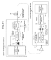
FIG. 11 is a diagram illustrating a configuration example of alight transmitting device 10 and alight receiving device 30 that employ a 43 Gbit/s RZ-DPSK or CSRZ-DPSK modulation method.FIG. 12 is a diagram illustrating the states of a light intensity and an optical phase when transmitting and receiving an optical signal modulated in a RZ-DPSK or CSRZ-DPSK modulation method. - In
FIG. 11 , thelight transmitting device 10 transmits an optical signal modulated in a 43 Gbit/s RZ-DPSK or CSRZ-DPSK modulation method. For example, thelight transmitting device 10 includes a transmitteddata processing unit 11, a CW (Continuous Wave)light source 12, aphase modulator 13, and an RZ-pulsed intensity modulator 14. - Specifically, the transmitted
data processing unit 11 has a function that acts as a framer that frames data to be input, a function that acts as an FEC (Forward Error Correction) encoder that provides an error correction code, and a function that acts as a DPSK precoder that performs an encoding process in which difference information between a code before one bit and a current code is reflected. - The
phase modulator 13 modulates the phase of continuous light output from theCW light source 12 in accordance with encoded data output from the transmitteddata processing unit 11, and outputs an optical signal of which the light intensity is constant and the binary optical phase carries on information, that is to say, an optical signal that is modulated in a DPSK method (see the lower stage ofFIG. 12 ). - The
intensity modulator 14 RZ-pulses the optical signal output from the phase modulator 13 (see the upper stage ofFIG. 12 ). Particularly, an RZ-DPSK signal indicates an optical signal RZ-pulsed by using a clock driving signal that has the same frequency (43 GHz) as the bit rate of data and an amplitude obtained by multiplying an extinction voltage (Vπ) by one. Moreover, a CSRZ-DPSK signal indicates an optical signal RZ-pulsed by using a clock driving signal that has a frequency (21.5 GHz) obtained by multiplying the bit rate of data by 1/2 and an amplitude obtained by multiplying an extinction voltage (Vπ) by two. - The
light receiving device 30 is connected to thelight transmitting device 10 via atransmission path 20 and anoptical repeater 21, and performs received signal processing on a (CS) RZ-DPSK signal output from thelight transmitting device 10 in an optical repeating transmission method. For example, thelight receiving device 30 includes adelay interferometer 31, a photo-electric converting unit 32, a reproducingcircuit 33, and a receiveddata processing unit 34. - Specifically, the
delay interferometer 31 is, for example, a Mach-Zehnder interferometer. Thedelay interferometer 31 causes a delay component of a one-bit time (23.3 ps in the configuration example ofFIG. 11 ) to interfere (delay-interfere) in a component on which a zero-radian phase control is performed, with respect to the (CS) RZ-DPSK signal transmitted through thetransmission path 20, and outputs the interference result as two outputs. In the Mach-Zehnder interferometer, a split wave guide is formed to be longer than another split wave guide by a propagation length corresponding to a one-bit time and an electrode is formed to control the phase of an optical signal propagating the other split wave guide. - The photo-
electric converting unit 32 is a dual pin photodiode that performs differential photoelectric conversion detection (balanced detection) by respectively receiving outputs from thedelay interferometer 31. In addition, a received signal detected by the photo-electric converting unit 32 is appropriately amplified by an amplifier. - The reproducing
circuit 33 extracts a data signal and a clock signal from the received signal detected by the photo-electric converting unit 32 in a differential photoelectric conversion method. The receiveddata processing unit 34 performs signal processing such as error correction based on the data signal and clock signal extracted by the reproducingcircuit 33. -
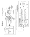
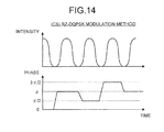
FIG. 13 is a diagram illustrating a configuration example of alight transmitting device 40 and alight receiving device 60 that employ a 43 Gbit/s RZ-DQPSK or CSRZ-DQPSK modulation method.FIG. 14 is a diagram illustrating the states of a light intensity and an optical phase when an RZ-DQPSK or CSRZ-DQPSK modulated optical signal is transmitted and received. - For example, in
FIG. 13 , thelight transmitting device 40 includes a transmitted data processing unit 41, a 1:2 separating unit (DMUX) 42, aCW light source 43, a π/2phase shifter 44, twophase modulators pulsed intensity modulator 46. - Specifically, the transmitted data processing unit 41 includes functions as a framer and an FEC encoder and a function as a DQPSK precoder that performs an encoding process in which difference information between a code before one bit and a current code is reflected, similarly to the transmitted
data processing unit 11 illustrated inFIG. 11 . - The 1:2 separating
unit 42 divides 43 Gbit/s encoded data output from the transmitted data processing unit 41 into 21.5 Gbit/s two-series encodeddata # 1 and #2. TheCW light source 43 outputs continuous light. The outputted continuous light is divided into two light beams. One light beam is input into thephase modulator 45A and the other light beam is input into thephase modulator 45B via the π/2phase shifter 44. - The
phase modulator 45A modulates the continuous light output from theCW light source 43 by using one-series encodeddata # 1 divided by the 1:2separating unit 42 and outputs an optical signal in which information is carried on a binary optical phase (0 radian or π radians). Moreover, thephase modulator 45B receives light that is obtained by phase-shifting the continuous light output from theCW light source 43 by π/2 in the π/2phase shifter 44, modulates the received light by using the other-series encodeddata # 2 separated by the 1:2 separatingunit 42, and outputs an optical signal in which information is carried on a binary optical phase (π/2 radians or 3π/2 radians. - The light modulated by the
phase modulators pulsed intensity modulator 46. In other words, modulated light output from thephase modulators FIG. 14 ) of which the light intensity is constant and information is carried on a four-value optical phase, that is to say, a DQPSK-modulated optical signal is sent to the RZ-pulsed intensity modulator 46. - The
intensity modulator 46 RZ-pulses the DQPSK-modulated optical signal output from thephase modulators intensity modulator 14 illustrated inFIG. 11 . Particularly, an RZ-DQPSK signal indicates an optical signal RZ-pulsed by using a clock driving signal that has the same frequency (21.5 GHz) as the bit rate ofdata # 1 and #2 and an amplitude obtained by multiplying an extinction voltage (Vπ) by one. Moreover, a CSRZ-DQPSK signal indicates an optical signal R2-puised by using a clock driving signal that has a frequency (10.75 GHz) obtained by multiplying the bit rate ofdata # 1 and #2 by 1/2 and an amplitude obtained by multiplying an extinction voltage (Vπ) by two. - The
light receiving device 60 is connected to thelight transmitting device 40 via atransmission path 50 and anoptical repeater 51, and performs received signal processing on the (CS) RZ-DQPSK signal output from thelight transmitting device 40 in an optical repeating transmission method. For example, thelight receiving device 60 includes asplitting unit 61 that splits the received optical signal into two. Thelight receiving device 60 further includesdelay interferometers units circuits light receiving device 60 includes a 2:1 multiplexing unit (MUX) 65 that multiplexes the data signal reproduced by the reproducingcircuits data processing unit 66. - Specifically, the
delay interferometers transmission path 50 and theoptical repeater 51 into two by using thesplitting unit 61. Thedelay interferometer 62A causes the delay component of a one-bit time (46.5 ps in the configuration example ofFIG. 13 ) to interfere (delay interfere) in a component on which the phase control of π/4 radians is performed, and outputs the interference result as two outputs. - Moreover, the
delay interferometer 62B causes the delay component of the one-bit time to interfere (delay interfere) in a component (the phase deviates by π/2 radians from the same component of thedelay interferometer 62A) on which the phase control of -π/4 radians is performed, and outputs the interference result as two outputs. In this case, each of thedelay interferometers electric converting units - The reproducing
circuit 64A reproduces an in-phase component I for the clock signal and data signal from the received signal detected by the photo-electric converting unit 63A in a differential photoelectric conversion method. Moreover, the reproducingcircuit 64B reproduces a quadrature-phase component Q for the clock signal and data signal from the received signal detected by the photo-electric converting unit 63B in a differential photoelectric conversion method. - The 2:1
multiplexing unit 65 receives the in-phase component I and the quadrature-phase component Q that are respectively output from the reproducingcircuits data processing unit 66 performs signal processing such as error correction based on the data signal output from the 2:1multiplexing unit 65. - Non-Patent Document 1: G. Charlet et al., "Non-liner Interactions between 10 Gb/s NRZ Channels and 40Gb/s Channels with RZ-DQPSK or PSBT Format over Low-Dispersion Fiber", ECOC 2006 Mo.3.2.6.
- As described above, a market demands the realization of a wavelength division multiplexing transmission system that operates based on a multiple signal obtained by mixing a 40 Gbit/s phase modulated signal (a signal modulated by (CS) RZ-DQPSK modulation method or (CS) RZ-DPSK modulation method) and a conventional 10(2.5) Gbit/s intensity modulated signal (a signal modulated by an NRZ method).
- However, when the wavelength division multiplexing transmission system is configured, the 40 Gbit/s phase modulated signal receives an optical phase shift caused by cross phase modulation (XPM) from the 10(2.5) Gbit/s intensity modulated signal. Therefore, there is a problem in that a waveform is conspicuously degraded and long distance transmission becomes difficult.
- In other words, it extremely becomes an important problem to prevent the waveform degradation (XPM degradation) of a phase modulated signal even if the phase modulated signal and the intensity modulated signal are wavelength-multiplexed.
- The present invention has been achieved in view of the above problems, and an object of the invention is to provide an optical signal processing apparatus that can prevent the waveform degradation (XPM degradation) of a phase modulated signal even if the phase modulated signal and the intensity modulated signal are wavelength-multiplexed.
- To solve the problems described above and achieve the object, the present invention is an optical signal processing apparatus for inserting and splitting an optical signal into and from an acquired multiple optical signal that is obtained by wavelength-multiplexing an optical signal modulated by a first modulation method and an optical signal modulated by a second modulation method.
The optical signal processing apparatus includes a wavelength selection switch that selects a predetermined wavelength from the multiple optical signal and outputs an optical signal having the selected wavelength to a predetermined output port. The wavelength selection switch has a different delay for each wavelength of the selected optical signal. - In the present invention, the wavelength selection switch includes a diffraction grating that separates the multiple optical signal for each wavelength; and a switching device array that includes a plurality of switching devices that respectively reflect optical signals having wavelengths separated by the diffraction grating and switch output ports that respectively output the optical signals having wavelengths by controlling angles thereof. Distances from the diffraction grating to the switching devices of the switching device array are different.
- In the present invention, the switching devices on the switching device array are arranged in the shape of saw.
- In the present invention, the switching devices on the switching device array are arranged in the shape of stairway.
- In the present invention, the wavelength selection switch includes a diffraction grating that separates the multiple optical signal for each wavelength; a plurality of switching device arrays that include a plurality of switching devices that respectively reflect optical signals having wavelengths separated by the diffraction grating and switch output ports that respectively output the optical signals having wavelengths by controlling angles thereof; and a separation switching device that divides the optical signals included in the multiple optical signal for each wavelength and reflects the divided optical signals toward the switching device arrays. Distances from the switching device arrays to the diffraction grating are different.
- In the present invention, the wavelength selection switch includes a diffraction grating that separates the multiple optical signal for each wavelength; a switching device array that includes a plurality of switching devices that respectively reflect optical signals having wavelengths separated by the diffraction grating and switch output ports that respectively output the optical signals having wavelengths by controlling angles thereof; and a fixed switching device that reflects the optical signals from the switching device array to the diffraction grating. The switching device array controls a central angle of the switching device to output an optical signal having one wavelength of adjacent wavelengths of the multiple optical signal to the output port via the fixed switching device.
- In the present invention, the wavelength selection switch includes a diffraction grating that separates the multiple optical signal for each wavelength; a switching device array that includes a plurality of switching devices that respectively reflect optical signals having wavelengths separated by the diffraction grating and switch output ports that respectively output the optical signals having wavelengths by controlling angles thereof; and a switching device unit that outputs one optical signal of optical signals having adjacent wavelengths among the optical signals from the switching device array to the output port via a fixed switching device.
- In the present invention, the wavelength selection switch includes a diffraction grating that separates the multiple optical signal for each wavelength; a switching device array that includes a plurality of switching devices that respectively reflect optical signals having wavelengths separated by the diffraction grating and switch output ports that respectively output the optical signals having wavelengths by controlling angles thereof; and a substrate that multiple-reflects only an optical signal corresponding to one wavelength of adjacent wavelengths and then transmits the multiple-reflected optical signal.
- In the present invention, the switching device array is a mirror array, and the mirror is a switching device.
- According to the present invention, the optical signal processing apparatus includes a wavelength selection switch that selects a predetermined wavelength from a multiple optical signal that is obtained by multiplexing an optical signal (a phase modulated signal) obtained by a first modulation method and an optical signal (an intensity modulated signal) obtained by a second modulation method and outputs the selected wavelength signal to a predetermined output port. Because the wavelength selection switch has a delay different for each wavelength of the multiple optical signal, the delay of the phase modulated signal and the intensity modulated signal is not identical to each other and the same position of the phase modulated signal does not continue to come under the influence of red chirp or blue chirp (the influence of red chirp or blue chirp is dispersed). Therefore, it is possible to prevent the waveform degradation (XPM degradation) of the phase modulated signal even if the phase modulated signal and the intensity modulated signal are wavelength-multiplexed.
-
-
FIG. 1 is a diagram illustrating XPM degradation between a phase modulated signal and an intensity modulated signal. -
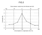
FIG. 2 is a diagram illustrating a relationship between a delay between an inline dispersion compensation ratio and a channel and a Q penalty. -
FIG. 3 is a diagram explaining the influence of an intensity modulated signal on a phase modulated signal. -
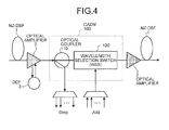
FIG. 4 is a functional block diagram illustrating the configuration of OADM according to a first embodiment of the present invention. -
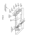
FIG. 5 is a diagram illustrating the configuration of a wavelength selection switch according to the first embodiment of the present invention. -
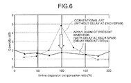
FIG. 6 is a diagram illustrating an effect when the OADM according to the first embodiment of the present invention is applied to a wavelength division multiplexing transmission system. -
FIG. 7 is a diagram illustrating the configuration of a wavelength selection switch according to a second embodiment of the present invention. -
FIG. 8 is a diagram illustrating the configuration of a wavelength selection switch according to a third embodiment of the present invention. -
FIG. 9 is a diagram illustrating the configuration of a wavelength selection switch according to a fourth embodiment of the present invention. -
FIG. 10 is a diagram illustrating the other configuration of the wavelength selection switch. -
FIG. 11 is a diagram illustrating a configuration example of a light transmitting device and a light receiving device that employ a 43 Gbit/s RZ-DPSK or CSRZ-DPSK modulation method. -
FIG. 12 is a diagram illustrating the states of a light intensity and an optical phase when an RZ-DPSK or CSRZ-DPSK modulated optical signal is transmitted and received. -
FIG. 13 is a diagram illustrating a configuration example of the light transmitting device and the light receiving device that employ a 43 Gbit/s RZ-DQPSK or CSRZ-DQPSK modulation method. -
FIG. 14 is a diagram illustrating the states of a light intensity and an optical phase when an RZ-DQPSK or CSRZ-DQPSK modulated optical signal is transmitted and received. -
FIG. 15 is a diagram illustrating a conventional wavelength division multiplexing transmission system that operates based on a multiple signal obtained by mixing a phase modulated signal and an intensity modulated signal. -
FIG. 16 is a functional block diagram illustrating the configuration of OADM. -
FIG. 17 is a diagram illustrating the configuration of a conventional wavelength selection switch. -
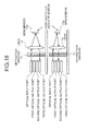
FIG. 18 is a diagram explaining the switching of an optical output port performed by a MEM mirror. -
- 1
- NZ-DSF
- 2
- Optical amplifier
- 3
- DCF
- 4, 100
- OADM
- 4a, 110
- Optical coupler
- 4b, 120, 300, 400
- Wavelength selection switch
- 5
- Wavelength multiplexer
- 6
- Wavelength demultiplexer
- 7
- Phase modulated signal transmitter
- 8
- Intensity modulated signal transmitter
- 9
- Phase modulated signal receiver
- 10, 40
- Light transmitting device
- 11, 41
- Transmitted data processing unit
- 12, 43
- CW light source
- 13, 45A, 45B
- Phase modulator
- 14, 46
- Intensity modulator
- 20, 50
- Transmission path
- 21, 51
- Optical repeater
- 30, 60
- Light receiving device
- 31, 62A, 62B
- Delay interferometer
- 32, 63A, 63B
- Photo-electric converting unit
- 33, 64A, 64B
- Reproducing circuit
- 34, 66
- Received data processing unit
- 42
- 1:2 DMUX
- 44
- π/2 phase shifter
- 61
- Splitting unit
- 65
- 2:1 MUX
- 121, 210, 310, 410
- Collimator lens
- 122, 220, 320, 420
- Diffraction grating
- 123, 230, 330a, 330b, 330c, 430
- Lens
- 124, 240, 350, 360, 450
- Mirror array
- 124a, 124b, 124c, 124d, 124e, 124f, 240a,
- 240b, 240c, 240d, 240e, 350a, 350b, 350c,
- 360a, 360b, 360c, 450a, 450b, 450c, 450d
- Mirror
- 440
- Reflecting mirror
- 440a, 440b
- Mirror unit
- Exemplary embodiments of an optical signal processing apparatus according to the present invention will be explained below in detail with reference to the accompanying drawings. The present invention is not limited to the embodiments explained below.
- Before explaining the embodiment of the present invention, it will be explained about a conventional wavelength division multiplexing transmission system that operates based on a multiple signal obtained by mixing a phase modulated signal (a signal modulated by a (CS) RZ-DPSK modulation method or a (CS) RZ-DQPSK modulation method) and an intensity modulated signal (a signal modulated by an NRZ modulation method).
FIG. 15 is a diagram illustrating a conventional wavelength division multiplexing transmission system that operates based on a multiple signal obtained by mixing a phase modulated signal and an intensity modulated signal. - As illustrated in the present drawing, the wavelength division multiplexing transmission system includes an NZ-DSF (Non-Zero Dispersion Shifted Fiber) 1, an
optical amplifier 2, a DCF (Dispersion Compensating Fiber) 3, an OADM (Optical Add-Drop Multiplexer) 4, awavelength multiplexer 5, awavelength demultiplexer 6, a phase modulatedsignal transmitter 7, an intensity modulatedsignal transmitter 8, and a phase modulatedsignal receiver 9. - Among them, the NZ-DSF (non-zero-dispersion shift single mode fiber) 1 is an optical fiber that slightly shifts a zero-dispersion wavelength from a 1550 nm band to suppress a nonlinear phenomenon at the 1550 nm band.
- The
optical amplifier 2 amplifies an optical signal. TheDCF 3 is a dispersion compensator (dispersion compensation fiber as a representative example) that compensates for the chromatic dispersion of optical signals that are transmitted on a transmission path NZ-DSF1. TheOADM 4 is an add-drop multiplexer that inserts or splits an optical signal assigned for each wavelength. -
FIG. 16 is a functional block diagram illustrating the configuration of theOADM 4. As illustrated in the present drawing, theOADM 4 includes anoptical coupler 4a and a wavelength selection switch (WSS) 4b. Theoptical coupler 4a is a device that splits an optical signal input into theOADM 4 into two or more outputs. - The
wavelength selection switch 4b is a switch that selects an arbitrary wavelength from the optical signal (wavelength-multiplexed optical signal) input into theOADM 4 and outputs an optical signal having the selected wavelength to an arbitrary optical output port.FIG. 17 is a diagram illustrating the configuration of the conventionalwavelength selection switch 4b. As illustrated in the present drawing, thewavelength selection switch 4b includes acollimator lens 70, adiffraction grating 71, alens 72, and anMEM mirror array 73. TheMEM mirror array 73 includes MEM mirrors 73a that respectively correspond to channels. - As the principle of the
wavelength selection switch 4b, thediffraction grating 71 spatially separates an optical signal input via the collimator lens (lens for forming parallel light) 70 and the rotation angles of the MEM mirrors 73a corresponding to channels (λ1, λ2, and the like) are controlled, in order to switch optical output ports. In addition, thelens 72 respectively matches the focal points of the optical signals output from thediffraction grating 71 with the MEM mirrors 73a. -
FIG. 18 is a diagram explaining the switching of the optical output ports performed by the MEM mirrors 73a. As illustrated in the present drawing, for example, a third optical output port can be switched to a second optical output port by adjusting the angles of the MEM mirrors 73a. - Referring to
FIG. 15 again, thewavelength multiplexer 5 multiplexes the phase modulated signal output from the phase modulatedsignal transmitter 7 and the intensity modulated signal output from the intensity modulatedsignal transmitter 8 and outputs the multiplexed optical signal to theOADM 4. - The
wavelength demultiplexer 6 demultiplexes, when acquiring an optical signal from theOADM 4, the acquired optical signal for each light wavelength and outputs, for example, the phase modulated signal output from the phase modulatedsignal transmitter 7 to the phase modulatedsignal receiver 9. Moreover, thewavelength demultiplexer 6 outputs the other optical signal (intensity modulated signal) to each intensity modulated signal receiver (not illustrated). - The phase modulated
signal transmitter 7 is a device that transmits, for example, an optical signal modulated by a 40 Gbit/s (CS) RZ-DPSK modulation method or (CS) RZ-DQPSK modulation method (specifically, seeFIGS. 11 to 14 ). The intensity modulatedsignal transmitter 8 is a device that outputs, for example, an optical signal modulated by a 10 Gbit/s or 2.5 Gbit/s NRZ modulation method. - The phase modulated
signal receiver 9 is connected to the phase modulatedsignal transmitter 7 via thewavelength multiplexer 5, theOADM 4, theoptical amplifier 2, NZ-DSF1, theDCF 3, and thewavelength demultiplexer 6. The phase modulatedsignal receiver 9 performs received signal processing on the phase modulated signal output from the phase modulatedsignal transmitter 7 in an optical repeating transmission method (specifically, seeFIGS. 11 to 14 ). - Next, it will be explained about XPM degradation caused by the wavelength division multiplexing transmission system illustrated in
FIG. 15 .FIG. 1 is a diagram illustrating XPM degradation between a phase modulated signal and an intensity modulated signal. InFIG. 1 , as an example, it is assumed that the transmission speed of the phase modulated signal is 40 Gbit/s and the transmission speed of the intensity modulated signal is 10 Gbit/s. InFIG. 1 , measurement results are illustrated when an optical signal is transmitted in the case of the 50 km NZ-DSF with 12 spans. Hereinafter, it is assumed that one span means the movement of optical signal from the output from the NZ-DSF to the input into the next NZ-DSF via the transmission path. - As illustrated in
FIG. 1 , when the phase modulated signal is one wave or when all the multiplexed optical signals are the phase modulated signal, a Q penalty goes low even if the intensity (for example, the intensity of the optical signal at the time point of the input from theoptical amplifier 2 into the transmission path) of the optical signal dominated by an optical fiber becomes high. A Q penalty is an index indicative of transmission signal quality. When the Q penalty is large, the symbol error rate of optical signal becomes large. - On the other hand, when a multiplexed optical signal includes a phase modulated signal and an intensity modulated signal (for example, when a multiplexed optical signal includes one phase modulated signal and four intensity modulated signals), the stronger the intensity of the optical signal input into the optical fiber becomes, the more the Q penalty becomes large. Particularly, when a relationship between the polarized wave of the phase modulated signal and the polarized wave of the intensity modulated signal is parallel, the Q penalty becomes large (the influence of XPM degradation becomes large).
- Next, it will be explained about a relationship between an inline dispersion compensation ratio in the NZ-DSF1 and the
DCF 3, a delay between adjacent channels per one span (hereinafter, a delay between channels), and a Q penalty. When the inline dispersion compensation ratio becomes 100%, an inline remaining dispersion amount becomes zero. An inline remaining dispersion amount indicates a remaining dispersion amount (average between spans) that occurs on the transmission path and in theDCF 3 per one span. -
FIG. 2 is a diagram illustrating a relationship between an inline dispersion compensation ratio, a delay between channels, and a Q penalty. As illustrated in the present drawing, in the vicinity of the point at which the inline dispersion compensation ratio becomes 100% or the delay between channels becomes 0 ps, it turns out that the Q penalty conspicuously occurs. This reason is that when the inline dispersion compensation ratio becomes 100%, the degradation of the phase modulated signal is conspicuously accumulated because the phase modulated signal continues to receive the chirp of the same code from the rising or trailing of the bit of the same intensity modulated signal in each relaying span. -
FIG. 3 is a diagram explaining an influence of an intensity modulated signal on a phase modulated signal. The phase modulated signal located at a first stage of the left side of the present drawing indicates an undegraded phase modulated signal before being influenced by an intensity modulated signal. In such a phase modulated signal (see the first stage of the left side ofFIG. 3 ), the instantaneous frequency of the phase modulated signal is shifted (red chirp) to a point at which a frequency is low (see a first stage of the right side ofFIG. 3 ) when being influenced by the rising (see a second stage of the left side ofFIG. 3 ) of the bit of the intensity modulated signal. - On the other hand, in the phase modulated signal (see the first stage of the left side of
FIG. 3 ), the instantaneous frequency of the phase modulated signal is shifted (blue chirp) to a point at which a frequency is high (see a second stage of the right side ofFIG. 3 ) when being influenced by the falling (see a third stage of the left side ofFIG. 3 ) of the bit of the intensity modulated signal. When the inline dispersion compensation ratio becomes about 100%, because the same position of the phase modulated signal continues to be influenced by red chirp or blue chirp, the optimum arrangement (a fourth stage of the left side ofFIG. 3 ) of the phase modulated signal degrades like a fourth stage of the right side ofFIG. 3 and thus the Q penalty becomes large. - Next, it will be explained about the brief and special feature of the OADM according to the first embodiment of the present invention. The OADM according to the first embodiment of the present invention has a wavelength selection switch that selects a predetermined wavelength from a multiple optical signal obtained by multiplexing a phase modulated signal and an intensity modulated signal and outputs the selected wavelength signal to a predetermined output port. The wavelength selection switch has a different delay for each wavelength of the multiple optical signal (the differential delay between channels is given from the inside of the wavelength selection switch).
- In this manner, in the OADM according to the first embodiment of the present invention, the delays of the phase modulated signal and the intensity modulated signal are not identical to each other because the differential delay between channels is given from the inside of the wavelength selection switch. Because the same position of the phase modulated signal does not continue to be influenced by red chirp or blue chirp (because the influence of red chirp or blue chirp is dispersed), the waveform degradation (XPM degradation) of the phase modulated signal can be prevented even if the phase modulated signal and the intensity modulated signal are wavelength-multiplexed.
-
FIG. 4 is a functional block diagram illustrating the configuration of anOADM 100 according to the first embodiment of the present invention. As illustrated in the present drawing, theOADM 100 includes anoptical coupler 110 and a wavelength selection switch (WSS) 120. Theoptical coupler 110 splits an optical signal input into theOADM 100 into two or more outputs. Thewavelength selection switch 120 is a switch that selects a predetermined wavelength from the optical signal (wavelength-multiplexed optical signal) input into theOADM 100 and outputs an optical signal having the selected wavelength to a predetermined optical output port. -
FIG. 5 is a diagram illustrating the configuration of thewavelength selection switch 120 according to the first embodiment of the present invention. As illustrated in the present drawing, thewavelength selection switch 120 includes acollimator lens 121, adiffraction grating 122, alens 123, and amirror array 124. - Among them, the
collimator lens 121 is a lens for forming parallel light. Thediffraction grating 122 separates a multiple optical signal for each wavelength. Thelens 123 adjusts the focal point of an optical signal that is output from thediffraction grating 122 to themirror array 124. - The mirror array (MEMS, liquid crystal, and the like) 124 includes a plurality of
mirrors 124a to 124f and is a device that controls the rotation angle of the mirror corresponding to each channel (wavelength λn) to switch output ports. In addition, the plurality ofmirrors 124a to 124f is arranged in the shape of saw on themirror array 124. - In an example illustrated in
FIG. 5 , themirror 124a selects the output port of the optical signal having a wavelength λ1. Themirror 124b selects the output port of the optical signal having a wavelength λ2. The mirror 124c selects the output port of the optical signal having a wavelength λ3. Themirror 124d selects the output port of the optical signal having a wavelength λ4. Themirror 124e selects the output port of the optical signal having a wavelength λ5. Themirror 124f selects the output port of the optical signal having a wavelength λ6. - As the principle of the
wavelength selection switch 120, thediffraction grating 122 spatially separates the optical signal input via thecollimator lens 121 and the rotation angles of themirrors 124a to 124f corresponding to channels (λ1, λ2, and the like) are controlled, in order to switch optical output ports. - Particularly, in the
wavelength selection switch 120 illustrated in the first embodiment of the present invention, as illustrated inFIG. 5 , optical paths from the surfaces of the mirrors to thediffraction grating 122 are different in the case of adjacent mirrors (for example, themirrors mirror array 124 on which one mirror is arranged is a first surface and the surface of themirror array 124 on which the other mirror is arranged is a second surface, the distance between the first surface and the second surface becomes not less than a predetermined value (for example, not less than 2 cm). - The distance between the first surface and the second surface is different depending on the transmission speed of intensity modulated signal. For example, when the transmission speed of intensity modulated signal is 10 Gbit/s, the distance between the first surface and the second surface is set to 2 cm or more. Moreover, when the transmission speed of intensity modulated signal is 2.5 Gbit/s, the distance between the first surface and the second surface is set to 8 cm or more. Furthermore, when the transmission speed of intensity modulated signal is 40 Gbit/s, the difference between the first surface and the second surface is set to 4 cm or more.
- In general, when the transmission speed of intensity modulated signal is M Gbit/s (M is an integer number not less than zero), the distance between the first surface and the second surface is set to become 20/M cm or more.
- In this manner, because optical paths from the mirrors to the
diffraction grating 122 are different by providing an optical path difference to the first surface and the second surface (arranging themirrors 124a to 124f in the shape of saw), delays between adjacent bits in a multiple optical signal are not identical to each other and thus the waveform degradation of phase modulated signal can be prevented. -
FIG. 6 is a diagram illustrating an effect when theOADM 100 according to the first embodiment of the present invention is applied to the wavelength division multiplexing transmission system. As illustrated in the present drawing, compared to a conventional wavelength transmission system, by applying theOADM 100 according to the first embodiment of the present invention to the wavelength division multiplexing transmission system, a Q penalty can be suppressed low even if an inline dispersion compensation ratio is 100%. - As described above, the
OADM 100 according to the first embodiment of the present invention has thewavelength selection switch 120 that selects a predetermined wavelength from a multiple optical signal obtained by multiplexing a phase modulated signal and an intensity modulated signal and outputs the selected wavelength signal to a predetermined output port and thewavelength selection switch 120 has a different delay for each wavelength of the multiple optical signal. Therefore, because the delays of the phase modulated signal and the intensity modulated signal are not identical to each other and the same position of the phase modulated signal does not continue to be influenced by red chirp or blue chirp (the influence of red chirp or blue chirp is dispersed), the waveform degradation (XPM degradation) of the phase modulated signal can be prevented even if the phase modulated signal and the intensity modulated signal are wavelength-multiplexed. - Even in the case of an existing relay node configuration or an existing transmission path dispersion map, a system that can reduce XPM degradation can be constructed simply and inexpensively in that XPM degradation can be solved by only the configuration change of the wavelength selection switch according to the first embodiment of the present invention.
- In addition, in the
wavelength selection switch 120 illustrated inFIG. 5 , beam diameters on the mirrors are different due to the focal-length relationship of the optical signal between adjacent channels (between even channel and odd channel) and thus the difference of coupling efficiency (optical loss) at module output ports can occur. However, because thewavelength selection switch 120 includes a compensating unit (not illustrated) that gives optical attenuation every wavelength, thewavelength selection switch 120 can compensate for an optical loss difference. - Next, it will be explained about an OADM according to the second embodiment of the present invention. The OADM according to the second embodiment of the present invention includes a waveform selection switch having the configuration different from that of the
OADM 100 illustrated in the first embodiment.FIG. 7 is a diagram illustrating the configuration of awavelength selection switch 200 according to the second embodiment of the present invention. As illustrated in the present drawing, thewavelength selection switch 200 includes acollimator lens 210, adiffraction grating 220, alens 230, and amirror array 240. - Among them, because the
collimator lens 210, thediffraction grating 220, and thelens 230 are similar to thecollimator lens 121, thediffraction grating 122, and thelens 123 illustrated inFIG. 5 , their descriptions are omitted. - The mirror array (MEMS, liquid crystal, and the like) 240 includes a plurality of
mirrors 240a to 240e. Themirror array 240 is a device that controls the rotation angles of the mirrors corresponding to channels (wavelength λn) to switch output ports. Moreover, the plurality ofmirrors 240a to 240e is arranged in the shape of stairway on themirror array 240. - In an example illustrated in
FIG. 7 , themirror 240a selects the output port of the optical signal having a wavelength λ1. Themirror 240b selects the output port of the optical signal having a wavelength λ2. Themirror 240c selects the output port of the optical signal having a wavelength λ3. Themirror 240d selects the output port of the optical signal having a wavelength λ4. Themirror 240e selects the output port of the optical signal having a wavelength λ5. - As the principle of the
wavelength selection switch 200, thediffraction grating 220 spatially separates the optical signal input via thecollimator lens 210 and the rotation angles of themirrors 240a to 240e corresponding to channels (λ1, λ2, ...) are controlled, in order to switch optical output ports. - Particularly, in the
wavelength selection switch 200 illustrated in the second embodiment of the present invention, as illustrated inFIG. 7 , optical paths from the surfaces of the mirrors to thediffraction grating 220 are different in the case of adjacent mirrors (for example, themirrors mirror array 240 on which one mirror is arranged is a first surface and the surface of themirror array 240 on which the other mirror is arranged is a second surface, the distance between the first surface and the second surface becomes not less than a predetermined value (for example, not less than 2 cm). - In addition, the distance between the first surface and the second surface is different depending on the transmission speed of intensity modulated signal. For example, when the transmission speed of intensity modulated signal is 10 Gbit/s, the distance between the first surface and the second surface is set to 2 cm or more. Moreover, when the transmission speed of intensity modulated signal is 2.5 Gbit/s, the distance between the first surface and the second surface is set to 8 cm or more. Furthermore, when the transmission speed of intensity modulated signal is 40 Gbit/s, the distance between the first surface and the second surface is set to 0.5 cm or more.
- In general, when the transmission speed of intensity modulated signal is M Gbit/s (M is an integer number not less than zero), the distance between the first surface and the second surface is set to become 20/M cm or more.
- In an example illustrated in
FIG. 7 , themirrors 240a to 240e are arranged on themirror array 240 in such a manner that optical paths between themirrors 240a to 240e and thediffraction grating 220 become large in the sequence of themirrors FIG. 7 , an optical path difference can be provided to adjacent optical signals by sequentially shifting the mirrors from themirror 240a to a predetermined mirror to the right. An optical path difference can be provided to adjacent optical signals by sequentially shifting the mirrors from a predetermined mirror to themirror 240e to the left. - By applying the OADM including the
wavelength selection switch 200 according to the second embodiment of the present invention to the wavelength division multiplexing transmission system, a Q penalty can be suppressed low even if an inline dispersion compensation ratio is 100% (seeFIG. 6 ). - As described above, the OADM according to the second embodiment of the present invention has the
wavelength selection switch 200 that selects a predetermined wavelength from a multiple optical signal obtained by multiplexing a phase modulated signal and an intensity modulated signal and outputs the selected wavelength signal to a predetermined output port and thewavelength selection switch 200 has a different delay for each wavelength of the multiple optical signal. Therefore, because the delays of the phase modulated signal and the intensity modulated signal are not identical to each other and the same position of the phase modulated signal does not continue to be influenced by red chirp or blue chirp (the influence of red chirp or blue chirp is dispersed), the waveform degradation (XPM degradation) of the phase modulated signal can be prevented even if the phase modulated signal and the intensity modulated signal are wavelength-multiplexed. - Next, it will be explained about an OADM according to the third embodiment of the present invention. The OADM according to the third embodiment of the present invention includes a wavelength selection switch having the configuration different from that of the OADM illustrated in the first and second embodiments.
FIG. 8 is a diagram illustrating the configuration of awavelength selection switch 300 according to the third embodiment of the present invention. As illustrated in the present drawing, thewavelength selection switch 300 includes acollimator lens 310, adiffraction grafting 320,lenses 330a to 330c, achannel separation mirror 340, andmirror arrays - Among them, because the
collimator lens 310, thediffraction grating 320, and thelens 330a are similar to thecollimator lens 121, thediffraction grating 122, and thelens 123 illustrated inFIG. 5 , their descriptions are omitted. - The
lens 330b adjusts the focal point of the optical signal that is reflected from thechannel separation mirror 340 to themirror array 350. Thelens 330c adjusts the focal point of the optical signal that is reflected from thechannel separation mirror 340 to themirror array 360. - The
channel separation mirror 340 receives an optical signal of each wavelength divided by thediffraction grating 320. Among the received optical signals, thechannel separation mirror 340 outputs the optical signals having wavelengths corresponding to odd channels (λ1, λ3, λ5, and the like) to themirror array 350 and outputs the optical signals having wavelengths corresponding to an even channels (λ2, λ4, λ6, and the like) to themirror array 360. - The
mirror array 350 includes a plurality ofmirrors 350a to 350c corresponding to odd channels. Themirror array 350 is a device that controls the rotation angles of the mirrors corresponding to the odd channels to switch output ports. - In an example illustrated in
FIG. 8 , themirror 350a selects the output port of the optical signal having a wavelength λ1. Themirror 350b selects the output port of the optical signal having a wavelength λ3. Themirror 350c selects the output port of the optical signal having a wavelength λ5. - The
mirror array 360 includes a plurality ofmirrors 360a to 360c corresponding to even channels. Themirror array 360 is a device that controls the rotation angles of the mirrors corresponding to the even channels to switch output ports. - In an example illustrated in
FIG. 8 , themirror 360a selects the output port of the optical signal having a wavelength λ2. Themirror 360b selects the output port of the optical signal having a wavelength λ4. Themirror 360c selects the output port of the optical signal having a wavelength λ6. - As the principle of the
wavelength selection switch 300, thediffraction grating 320 spatially separates the optical signal input via thecollimator lens 310, themirror array 350 controls the rotation angles of themirrors 350a to 350c corresponding to odd channels, and themirror array 360 controls the rotation angles of themirrors 360a to 360c corresponding to even channels, in order to switch optical output ports. - Particularly, in the
wavelength selection switch 300 illustrated in the third embodiment of the present invention, as illustrated inFIG. 8 , optical paths from the mirror array 350 (themirrors 350a to 350c) to thediffraction grating 320 and optical paths from the mirror array 360 (themirrors 360a to 360c) to thediffraction grating 320 are different. Specifically, the distance between the mirror array 350 (the surfaces of themirrors 350a to 350c) and the mirror array 360 (the surfaces of themirrors 360a to 360c) becomes not less than a predetermined value (for example, 2 cm or more). - In addition, the difference between the
mirror array 350 and themirror array 360 is different depending on the transmission speed of intensity modulated signal. For example, when the transmission speed of intensity modulated signal is 10 Gbit/s, the distance between a first surface (the surface of the mirror array 350) and a second surface (the surface of the mirror array 360) is set to 2 cm or more. Moreover, when the transmission speed of intensity modulated signal is 2.5 Gbit/s, the distance between the first surface and the second surface is set to 8 cm or more. Furthermore, when the transmission speed of intensity modulated signal is 40 Gbit/s, the distance between the first surface and the second surface is set to 0.5 cm or more. - In general, when the transmission speed of intensity modulated signal is M Gbit/s (M is an integer number not less than zero), the distance between the
mirror array 350 and themirror array 360 is set to become 20/M cm or more. - As illustrated in
FIG. 8 , because the optical paths from themirror array 350 to thediffraction grating 320 and the optical paths from themirror array 360 to thediffraction grating 320 are different by arranging themirror array 350 and themirror array 360, delays between adjacent bits in a multiple Optical signal are not identical to each other and thus the waveform degradation of phase modulated signal can be prevented. - By applying the OADM including the
wavelength selection switch 300 according to the third embodiment of the present invention to the wavelength division multiplexing transmission system, a Q penalty can be suppressed low even if an inline dispersion compensation ratio is 100% (seeFIG. 6 ). - As described above, the OADM according to the third embodiment of the present invention has the
wavelength selection switch 300 that selects a predetermined wavelength from a multiple optical signal obtained by multiplexing a phase modulated signal and an intensity modulated signal and outputs the selected wavelength signal to a predetermined output port and thewavelength selection switch 300 has a different delay for each wavelength of the multiple optical signal. Therefore, because the delays of the phase modulated signal and the intensity modulated signal are not identical to each other and the same position of the phase modulated signal does not continue to be influenced by red chirp or blue chirp (the influence of red chirp or blue chirp is dispersed), the waveform degradation (XPM degradation) of the phase modulated signal can be prevented even if the phase modulated signal and the intensity modulated signal are wavelength-multiplexed. - Next, it will be explained about an OADM according to the fourth embodiment of the present invention. The OADM according to the fourth embodiment of the present invention includes a wavelength selection switch having the configuration different from that of the OADM illustrated in the first to third embodiments.
FIG. 9 is a diagram illustrating the configuration of awavelength selection switch 400 according to the fourth embodiment of the present invention. As illustrated in the present drawing, thewavelength selection switch 400 includes acollimator lens 410, adiffraction grating 420, alens 430, a reflectingmirror 440, and amirror array 450. - Among them, because the
collimator lens 410, thediffraction grating 420, and thelens 430 are similar to thecollimator lens 121, thediffraction grating 122, and thelens 123 illustrated inFIG. 5 , their descriptions are omitted. - The reflecting
mirror 440 receives the optical signals (for example, optical signals from themirrors mirrors 450a and 450c) having wavelengths corresponding to even channels (or odd channels) and outputs the received optical signals to thediffraction grating 420. - The
mirror array 450 includes a plurality of mirrors 450a to 450d. Themirror array 450 is a device that controls the rotation angles of the mirrors 450a to 450d to switch output ports. - In an example illustrated in
FIG. 9 , the mirror 450a selects the output port of the optical signal having a wavelength λ1. Themirror 450b selects the output port of the optical signal having a wavelength λ2. Themirror 450c selects the output port of the optical signal having a wavelength λ3. Themirror 450d selects the output port of the optical signal having a wavelength λ4. - Particularly, in the
wavelength selection switch 400 illustrated in the third embodiment of the present invention, by controlling the central angles of the mirrors (themirrors mirrors 450a and 450c) for odd channels, the difference is caused between optical paths from the mirrors for even channels to thediffraction grating 420 and optical paths from the mirrors for odd channels to thediffraction grating 420. - For example, a control unit (not illustrated) controls the central angles of the mirrors for even channels to set components in such a manner that the optical signals from the mirrors for even channels arrive at the
diffraction grating 420 via the reflectingmirror 440 and holds the central angles of the mirrors for odd channels without change to set the components in such a manner that the optical signals from the mirrors for odd channels arrive at thediffraction grating 420 without passing through the reflectingmirror 440. - As illustrated in
FIG. 9 , by controlling the central angles of the mirrors for even channels or the mirrors for odd channels, the optical paths of the optical signals of even channels and the optical paths of the optical signals of odd channels are different, the delays between adjacent bits in the multiple optical signal are not identical to each other, and the waveform degradation of phase modulated signal can be prevented. - By applying the OADM including the
wavelength selection switch 400 according to the fourth embodiment of the present invention to the wavelength division multiplexing transmission system, a Q penalty can be suppressed low even if an inline dispersion compensation ratio is 100% (seeFIG. 6 ). - As described above, the OADM according to the fourth embodiment of the present invention has the
wavelength selection switch 400 that selects a predetermined wavelength from a multiple optical signal obtained by multiplexing a phase modulated signal and an intensity modulated signal and outputs the selected wavelength signal to a predetermined output port and thewavelength selection switch 400 has a different delay for each wavelength of the multiple optical signal. Therefore, because the delays of the phase modulated signal and the intensity modulated signal are not identical to each other and the same position of the phase modulated signal does not continue to be influenced by red chirp or blue chirp (the influence of red chirp or blue chirp is dispersed), the waveform degradation (XPM degradation) of the phase modulated signal can be prevented even if the phase modulated signal and the intensity modulated signal are wavelength-multiplexed. - In addition, the
wavelength selection switch 400 illustrated inFIG. 9 controls the central angles of the mirrors for even channels or the mirrors for odd channels and outputs the optical signals to thediffraction grating 420 via the reflectingmirror 440 in order to prevent the delays of adjacent optical signals from being identical to each other. However, the present invention is not limited to this. For example, by providing a mirror unit between thelens 430 and themirror array 450, the optical signals from the mirrors for even channels or the mirrors for odd channels can be directed to the reflectingmirror 440 without controlling the central angles of the mirrors. -
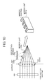
FIG. 10 is a diagram illustrating another configuration of thewavelength selection switch 400. As illustrated in the present drawing, there are provided amirror unit 440a that reflects optical signals having wavelengths corresponding to even channels or odd channels toward the reflectingmirror 440 and amirror unit 440b that receives the optical signals reflected from the reflectingmirror 440 and reflects the received optical signals to thediffraction grating 420. - In
FIG. 10 , the right side thereof illustrates the configuration of themirror unit 440a. When reflecting the optical signals having wavelengths corresponding to even channels toward the reflectingmirror 440, the mirror coatings of themirror unit 440a are provided at the positions at which the optical signals from themirrors mirrors 450a and 450c arrive at thediffraction grating 420 without being reflected on themirror units - On the other hand, when reflecting the optical signals having wavelengths corresponding to odd channels toward the reflecting
mirror 440, the mirror coatings of themirror unit 440a are provided at the positions at which the optical signals from themirrors 450a and 450c pass.
In this case, the optical signals from themirrors diffraction grating 420 without being reflected on themirror units - In this manner, by using the reflecting
mirror 440 and themirror units - Alternatively, it is possible to prevent the delays of adjacent optical signals from being identical to each other even when a saw-shaped transmission substrate (hereinafter, "substrate") is provided between the
diffraction grating 71 and theMEM mirror array 73 of thewavelength selection switch 4b illustrated inFIG. 17 . - Specifically, after the refractive indices of the positions at which the optical signals of even channels pass are previously adjusted on the substrate and the optical signals of even channels are multiple-reflected inside the substrate, the optical signals are output to the
MEM mirror array 73. The optical signals corresponding to odd channels are not multiple-reflected inside the substrate and are output to theMEM mirror array 73. In this way, it is possible to prevent the delays of adjacent optical signals from being identical to each other. - On the contrary, after the refractive indices of the positions at which the optical signals of odd channels pass are previously adjusted on a substrate and the optical signals of odd channels are multiple-reflected inside the substrate, the optical signals are output to the
MEM mirror array 73. The optical signals corresponding to even channels are not multiple-reflected inside the substrate and are output to theMEM mirror array 73. In this way, it is possible to prevent the delays of adjacent optical signals from being identical to each other. - Among the processes described in the first to fourth embodiments of the present invention, the whole or a part of the processes that are automatically performed can be manually performed. Alternatively, the whole or a part of the processes that are manually performed can be automatically performed in a well-known method.
- Moreover, the wavelength selection switch illustrated in the first to fourth embodiments of the present invention is a functional and conceptual switch. Therefore, the wavelength selection switch does not necessarily have the physical configuration as illustrated. In other words, the specific configuration of dispersion/integration of each device is not limited to the illustrated configuration. The whole or a part of the specific configuration can be dispersed or integrated functionally or physically in an optional unit in accordance with various types of loads, the status of use, or the like.
- In the first to fourth embodiments of the present invention, as an example, it has been explained about the principle of the wavelength selection switch based on a MEMS type. However, a liquid crystal wavelength selection switch as disclosed in Non-Patent Document (Glenn Baxter, "Highly programmable Wavelength Selective Switch based on Liquid Crystal on Silicon switching elements", OFC NFOEC 2006) can be utilized instead of the wavelength selection switch. In other words, a switching device array can be utilized instead of the mirror arrays (124, 240, 350, 360, and 450) explained in the embodiments. A switching device and the like can be utilized instead of the mirrors (124a, 124b, 124c, 124d, 124e, 124f, 240a, 240b, 240c, 240d, 240e, 350a, 350b, 350c, 360a, 360b, 360c, 450a, 450b, 450c, and 450d), the reflecting
mirror 440, and themirror units - In the first to fourth embodiments of the present invention, it has been explained about a mixed system of a phase modulation method and an intensity modulation method. However, the present invention is not limited to this. The wavelength selection switch explained in the first to fourth embodiments can be applied to a wavelength division multiplex system for only an intensity modulation method.
- Because waveform degradation caused by cross phase modulation (XPM) is conspicuously seen in a mixed system, the present invention has a large effect in the mixed system. On the other hand, because waveform degradation caused by cross phase modulation (XPM) slightly occurs even in a wavelength division multiplex system (for example, a 10 Gbit/s NRZ-signal wavelength division multiplex) for only an intensity modulation method, waveform degradation can be suppressed by applying the wavelength selection switch according to the present invention to the wavelength division multiplex system.
- As above, the optical signal processing apparatus according to the present invention is useful for the wavelength division multiplexing transmission system that multiplexes and transmits optical signals. Particularly, even if optical signals modulated by different modulation methods are multiplexed, the optical signal processing apparatus is suitable when it is necessary to prevent the degradation of optical signals.
Claims (9)
- An optical signal processing apparatus for inserting and splitting an optical signal into and from an acquired multiple optical signal that is obtained by wavelength-multiplexing an optical signal modulated by a first modulation method and an optical signal modulated by a second modulation method, the optical signal processing apparatus comprising:a wavelength selection switch that selects a predetermined wavelength from the multiple optical signal and outputs an optical signal having the selected wavelength to a predetermined output port, whereinthe wavelength selection switch has a different delay for each wavelength of the selected optical signal.
- The optical signal processing apparatus according to claim 1, wherein
the wavelength selection switch includesa diffraction grating that separates the multiple optical signal for each wavelength; anda switching device array that includes a plurality of switching devices that respectively reflect optical signals having wavelengths separated by the diffraction grating and switch output ports that respectively output the optical signals having wavelengths by controlling angles thereof, anddistances from the diffraction grating to the switching devices of the switching device array are different. - The optical signal processing apparatus according to claim 2, wherein the switching devices on the switching device array are arranged in the shape of saw.
- The optical signal processing apparatus according to claim 2, wherein the switching devices on the switching device array are arranged in the shape of stairway.
- The optical signal processing apparatus according to claim 1, wherein
the wavelength selection switch includesa diffraction grating that separates the multiple optical signal for each wavelength;a plurality of switching device arrays that include a plurality of switching devices that respectively reflect optical signals having wavelengths separated by the diffraction grating and switch output ports that respectively output the optical signals having wavelengths by controlling angles thereof; anda separation switching device that divides the optical signals included in the multiple optical signal for each wavelength and reflects the divided optical signals toward the switching device arrays, anddistances from the switching device arrays to the diffraction grating are different. - The optical signal processing apparatus according to claim 1, wherein
the wavelength selection switch includesa diffraction grating that separates the multiple optical signal for each wavelength;a switching device array that includes a plurality of switching devices that respectively reflect optical signals having wavelengths separated by the diffraction grating and switch output ports that respectively output the optical signals having wavelengths by controlling angles thereof; anda fixed switching device that reflects the optical signals from the switching device array to the diffraction grating, andthe switching device array controls a central angle of the switching device to output an optical signal having one wavelength of adjacent wavelengths of the multiple optical signal to the output port via the fixed switching device. - The optical signal processing apparatus according to claim 1, wherein
the wavelength selection switch includesa diffraction grating that separates the multiple optical signal for each wavelength;a switching device array that includes a plurality of switching devices that respectively reflect optical signals having wavelengths separated by the diffraction grating and switch output ports that respectively output the optical signals having wavelengths by controlling angles thereof; anda switching device unit that outputs one optical signal of optical signals having adjacent wavelengths among the optical signals from the switching device array to the output port via a fixed switching device. - The optical signal processing apparatus according to claim 1, wherein
the wavelength selection switch includesa diffraction grating that separates the multiple optical signal for each wavelength;a switching device array that includes a plurality of switching devices that respectively reflect optical signals having wavelengths separated by the diffraction grating and switch output ports that respectively output the optical signals having wavelengths by controlling angles thereof; anda substrate that multiple-reflects only an optical signal corresponding to one wavelength of adjacent wavelengths and then transmits the multiple-reflected optical signal. - The optical signal processing apparatus according to any one of claims 2 to 8, whereinthe switching device array is a mirror array, andthe mirror is a switching device.
Applications Claiming Priority (1)
| Application Number | Priority Date | Filing Date | Title |
|---|---|---|---|
| PCT/JP2007/067151 WO2009031196A1 (en) | 2007-09-03 | 2007-09-03 | Optical signal processor |
Publications (3)
| Publication Number | Publication Date |
|---|---|
| EP2182399A1 true EP2182399A1 (en) | 2010-05-05 |
| EP2182399A4 EP2182399A4 (en) | 2013-03-27 |
| EP2182399B1 EP2182399B1 (en) | 2017-08-16 |
Family
ID=40428519
Family Applications (1)
| Application Number | Title | Priority Date | Filing Date |
|---|---|---|---|
| EP07806619.8A Not-in-force EP2182399B1 (en) | 2007-09-03 | 2007-09-03 | Optical signal processor |
Country Status (4)
| Country | Link |
|---|---|
| US (1) | US8331779B2 (en) |
| EP (1) | EP2182399B1 (en) |
| JP (1) | JP5445132B2 (en) |
| WO (1) | WO2009031196A1 (en) |
Families Citing this family (10)
| Publication number | Priority date | Publication date | Assignee | Title |
|---|---|---|---|---|
| JP5645374B2 (en) | 2009-06-30 | 2014-12-24 | 日本オクラロ株式会社 | Interferometer, demodulator and optical communication module |
| JP5737874B2 (en) | 2010-07-06 | 2015-06-17 | 日本オクラロ株式会社 | Demodulator and optical transceiver |
| JP5850313B2 (en) * | 2011-10-05 | 2016-02-03 | 国立大学法人名古屋大学 | Wavelength group optical path cross-connect equipment |
| JP6021492B2 (en) * | 2012-07-27 | 2016-11-09 | 国立研究開発法人科学技術振興機構 | Optical cross-connect device |
| US10142030B1 (en) * | 2017-12-07 | 2018-11-27 | Booz Allen Hamilton Inc. | M-ARY frequency presence modulation communication system and method |
| CN113156585B (en) * | 2020-01-23 | 2025-11-14 | 华为技术有限公司 | A wavelength selective switch WSS |
| US10903930B1 (en) * | 2020-01-31 | 2021-01-26 | Fujitsu Limited | In-service defragmentation in optical networks using wavelength conversion |
| US11212010B2 (en) * | 2020-03-17 | 2021-12-28 | Raytheon Company | Optically-steered RF imaging receiver using photonic spatial beam processing |
| US11664905B2 (en) | 2020-03-17 | 2023-05-30 | Raytheon Company | Optically-steered RF imaging receiver using photonic spatial beam processing |
| US11909439B2 (en) * | 2021-04-23 | 2024-02-20 | SA Photonics, Inc. | Wavefront sensor with inner detector and outer detector |
Family Cites Families (11)
| Publication number | Priority date | Publication date | Assignee | Title |
|---|---|---|---|---|
| US6501877B1 (en) * | 1999-11-16 | 2002-12-31 | Network Photonics, Inc. | Wavelength router |
| US7236660B2 (en) * | 2002-05-20 | 2007-06-26 | Jds Uniphase Corporation | Reconfigurable optical add-drop module, system and method |
| JP3852409B2 (en) * | 2003-02-04 | 2006-11-29 | 富士通株式会社 | Optical functional device |
| JP2005070546A (en) * | 2003-08-26 | 2005-03-17 | Fujitsu Ltd | Polarization-controlled wavelength selective switch |
| JP2006133298A (en) * | 2004-11-02 | 2006-05-25 | Nikon Corp | Wavelength selective switch |
| JP4500720B2 (en) * | 2005-03-29 | 2010-07-14 | 富士通株式会社 | Light switch |
| US7263253B2 (en) * | 2005-04-11 | 2007-08-28 | Capella Photonics, Inc. | Optimized reconfigurable optical add-drop multiplexer architecture with MEMS-based attenuation or power management |
| JP2006343628A (en) * | 2005-06-10 | 2006-12-21 | Nikon Corp | Wavelength selective switch |
| JP4489678B2 (en) | 2005-09-30 | 2010-06-23 | 富士通株式会社 | Wavelength selective optical switch and optical device with spectroscopic function |
| EP1819072B1 (en) * | 2006-02-14 | 2012-11-28 | Alcatel Lucent | Optical network element with dispersion compensation |
| US7440650B2 (en) * | 2006-08-03 | 2008-10-21 | Jds Uniphase Corporation | Planar lightwave circuit based wavelength selective switch |
-
2007
- 2007-09-03 JP JP2009531037A patent/JP5445132B2/en not_active Expired - Fee Related
- 2007-09-03 WO PCT/JP2007/067151 patent/WO2009031196A1/en not_active Ceased
- 2007-09-03 EP EP07806619.8A patent/EP2182399B1/en not_active Not-in-force
-
2010
- 2010-03-02 US US12/659,270 patent/US8331779B2/en not_active Expired - Fee Related
Also Published As
| Publication number | Publication date |
|---|---|
| JP5445132B2 (en) | 2014-03-19 |
| JPWO2009031196A1 (en) | 2010-12-09 |
| US8331779B2 (en) | 2012-12-11 |
| US20100221002A1 (en) | 2010-09-02 |
| EP2182399B1 (en) | 2017-08-16 |
| EP2182399A4 (en) | 2013-03-27 |
| WO2009031196A1 (en) | 2009-03-12 |
Similar Documents
| Publication | Publication Date | Title |
|---|---|---|
| EP2182399B1 (en) | Optical signal processor | |
| US7536108B2 (en) | High precision chromatic dispersion measuring method and automatic dispersion compensating optical link system that uses this method | |
| EP1895690B1 (en) | Optical transmission apparatus | |
| US7515834B2 (en) | Upgraded optical communication system with increased transmission capacity and method | |
| CN101621336B (en) | Difference quadrature phase keying system, method and device | |
| US20050008369A1 (en) | Optical device with tunable coherent receiver | |
| JP4701192B2 (en) | Transmission system and transmission method | |
| US7277647B2 (en) | System and method of optical transmission | |
| US8098996B2 (en) | Adaptable duobinary generating filters, transmitters, systems and methods | |
| US20130177316A1 (en) | Optical communication system, and transmitter and receiver apparatus therefor | |
| EP2260588B1 (en) | Method and apparatus for demodulating and regenerating phase modulated optical signals | |
| Winzer et al. | 10× 107-Gb/s NRZ-DQPSK transmission at 1.0 b/s/Hz over 12× 100 km including 6 optical routing nodes | |
| EP1475914B1 (en) | Network element for use in an optical communication network, in particular a DWDM communication network | |
| JP5321591B2 (en) | Optical transmitter, optical receiver, and optical communication system | |
| JP3708503B2 (en) | High-accuracy chromatic dispersion measuring method and automatic dispersion compensating optical link system using the same | |
| US8320777B2 (en) | Temperature controlled interferometer for phase demodulation | |
| JPWO2009013795A1 (en) | Optical transmission apparatus, wavelength division multiplexing optical communication system, and optical transmission method | |
| JP4675796B2 (en) | Automatic dispersion compensating optical transmission system | |
| US20080199189A1 (en) | Colorless optical demodulator for differential quadrature phase shift keying dwdm systems | |
| US8811827B2 (en) | System for generating optical RZ signals based on electrical RZ signals | |
| JP4056954B2 (en) | WDM transmission system and WDM transmission method | |
| JP2004343360A (en) | Optical transmission device and optical communication system | |
| Gnauck et al. | Optical duobinary format from demodulation of DPSK using athermal delay interferometer | |
| Liu et al. | Optical technologies and techniques for high bit rate fiber transmission | |
| Liu et al. | Direct Detection of 107-Gb/s polarization-multiplexed DQPSK with electronic polarization demultiplexing |
Legal Events
| Date | Code | Title | Description |
|---|---|---|---|
| PUAI | Public reference made under article 153(3) epc to a published international application that has entered the european phase |
Free format text: ORIGINAL CODE: 0009012 |
|
| 17P | Request for examination filed |
Effective date: 20100303 |
|
| AK | Designated contracting states |
Kind code of ref document: A1 Designated state(s): AT BE BG CH CY CZ DE DK EE ES FI FR GB GR HU IE IS IT LI LT LU LV MC MT NL PL PT RO SE SI SK TR |
|
| AX | Request for extension of the european patent |
Extension state: AL BA HR MK RS |
|
| DAX | Request for extension of the european patent (deleted) | ||
| A4 | Supplementary search report drawn up and despatched |
Effective date: 20130225 |
|
| RIC1 | Information provided on ipc code assigned before grant |
Ipc: H04B 10/27 20130101ALI20130219BHEP Ipc: G02B 26/08 20060101AFI20130219BHEP Ipc: H04Q 3/52 20060101ALI20130219BHEP Ipc: H04Q 11/00 20060101ALI20130219BHEP Ipc: H04J 14/02 20060101ALI20130219BHEP |
|
| REG | Reference to a national code |
Ref country code: DE Ref legal event code: R079 Ref document number: 602007052027 Country of ref document: DE Free format text: PREVIOUS MAIN CLASS: G02B0026080000 Ipc: G02B0006350000 |
|
| RIC1 | Information provided on ipc code assigned before grant |
Ipc: H04Q 11/00 20060101ALI20170215BHEP Ipc: H04J 14/02 20060101ALI20170215BHEP Ipc: G02B 6/293 20060101ALI20170215BHEP Ipc: H04Q 3/52 20060101ALI20170215BHEP Ipc: G02B 6/35 20060101AFI20170215BHEP |
|
| GRAP | Despatch of communication of intention to grant a patent |
Free format text: ORIGINAL CODE: EPIDOSNIGR1 |
|
| INTG | Intention to grant announced |
Effective date: 20170324 |
|
| GRAS | Grant fee paid |
Free format text: ORIGINAL CODE: EPIDOSNIGR3 |
|
| GRAA | (expected) grant |
Free format text: ORIGINAL CODE: 0009210 |
|
| AK | Designated contracting states |
Kind code of ref document: B1 Designated state(s): AT BE BG CH CY CZ DE DK EE ES FI FR GB GR HU IE IS IT LI LT LU LV MC MT NL PL PT RO SE SI SK TR |
|
| REG | Reference to a national code |
Ref country code: GB Ref legal event code: FG4D |
|
| REG | Reference to a national code |
Ref country code: FR Ref legal event code: PLFP Year of fee payment: 11 |
|
| REG | Reference to a national code |
Ref country code: CH Ref legal event code: EP |
|
| REG | Reference to a national code |
Ref country code: IE Ref legal event code: FG4D |
|
| REG | Reference to a national code |
Ref country code: AT Ref legal event code: REF Ref document number: 919603 Country of ref document: AT Kind code of ref document: T Effective date: 20170915 |
|
| REG | Reference to a national code |
Ref country code: DE Ref legal event code: R096 Ref document number: 602007052027 Country of ref document: DE |
|
| PGFP | Annual fee paid to national office [announced via postgrant information from national office to epo] |
Ref country code: DE Payment date: 20170818 Year of fee payment: 11 Ref country code: FR Payment date: 20170818 Year of fee payment: 11 Ref country code: GB Payment date: 20170824 Year of fee payment: 11 |
|
| REG | Reference to a national code |
Ref country code: NL Ref legal event code: MP Effective date: 20170816 |
|
| REG | Reference to a national code |
Ref country code: LT Ref legal event code: MG4D |
|
| REG | Reference to a national code |
Ref country code: AT Ref legal event code: MK05 Ref document number: 919603 Country of ref document: AT Kind code of ref document: T Effective date: 20170816 |
|
| PG25 | Lapsed in a contracting state [announced via postgrant information from national office to epo] |
Ref country code: FI Free format text: LAPSE BECAUSE OF FAILURE TO SUBMIT A TRANSLATION OF THE DESCRIPTION OR TO PAY THE FEE WITHIN THE PRESCRIBED TIME-LIMIT Effective date: 20170816 Ref country code: LT Free format text: LAPSE BECAUSE OF FAILURE TO SUBMIT A TRANSLATION OF THE DESCRIPTION OR TO PAY THE FEE WITHIN THE PRESCRIBED TIME-LIMIT Effective date: 20170816 Ref country code: NL Free format text: LAPSE BECAUSE OF FAILURE TO SUBMIT A TRANSLATION OF THE DESCRIPTION OR TO PAY THE FEE WITHIN THE PRESCRIBED TIME-LIMIT Effective date: 20170816 Ref country code: AT Free format text: LAPSE BECAUSE OF FAILURE TO SUBMIT A TRANSLATION OF THE DESCRIPTION OR TO PAY THE FEE WITHIN THE PRESCRIBED TIME-LIMIT Effective date: 20170816 Ref country code: SE Free format text: LAPSE BECAUSE OF FAILURE TO SUBMIT A TRANSLATION OF THE DESCRIPTION OR TO PAY THE FEE WITHIN THE PRESCRIBED TIME-LIMIT Effective date: 20170816 |
|
| PG25 | Lapsed in a contracting state [announced via postgrant information from national office to epo] |
Ref country code: GR Free format text: LAPSE BECAUSE OF FAILURE TO SUBMIT A TRANSLATION OF THE DESCRIPTION OR TO PAY THE FEE WITHIN THE PRESCRIBED TIME-LIMIT Effective date: 20171117 Ref country code: PL Free format text: LAPSE BECAUSE OF FAILURE TO SUBMIT A TRANSLATION OF THE DESCRIPTION OR TO PAY THE FEE WITHIN THE PRESCRIBED TIME-LIMIT Effective date: 20170816 Ref country code: BG Free format text: LAPSE BECAUSE OF FAILURE TO SUBMIT A TRANSLATION OF THE DESCRIPTION OR TO PAY THE FEE WITHIN THE PRESCRIBED TIME-LIMIT Effective date: 20171116 Ref country code: ES Free format text: LAPSE BECAUSE OF FAILURE TO SUBMIT A TRANSLATION OF THE DESCRIPTION OR TO PAY THE FEE WITHIN THE PRESCRIBED TIME-LIMIT Effective date: 20170816 Ref country code: LV Free format text: LAPSE BECAUSE OF FAILURE TO SUBMIT A TRANSLATION OF THE DESCRIPTION OR TO PAY THE FEE WITHIN THE PRESCRIBED TIME-LIMIT Effective date: 20170816 Ref country code: IS Free format text: LAPSE BECAUSE OF FAILURE TO SUBMIT A TRANSLATION OF THE DESCRIPTION OR TO PAY THE FEE WITHIN THE PRESCRIBED TIME-LIMIT Effective date: 20171216 |
|
| PG25 | Lapsed in a contracting state [announced via postgrant information from national office to epo] |
Ref country code: CZ Free format text: LAPSE BECAUSE OF FAILURE TO SUBMIT A TRANSLATION OF THE DESCRIPTION OR TO PAY THE FEE WITHIN THE PRESCRIBED TIME-LIMIT Effective date: 20170816 Ref country code: RO Free format text: LAPSE BECAUSE OF FAILURE TO SUBMIT A TRANSLATION OF THE DESCRIPTION OR TO PAY THE FEE WITHIN THE PRESCRIBED TIME-LIMIT Effective date: 20170816 Ref country code: DK Free format text: LAPSE BECAUSE OF FAILURE TO SUBMIT A TRANSLATION OF THE DESCRIPTION OR TO PAY THE FEE WITHIN THE PRESCRIBED TIME-LIMIT Effective date: 20170816 |
|
| REG | Reference to a national code |
Ref country code: CH Ref legal event code: PL |
|
| REG | Reference to a national code |
Ref country code: DE Ref legal event code: R097 Ref document number: 602007052027 Country of ref document: DE |
|
| PG25 | Lapsed in a contracting state [announced via postgrant information from national office to epo] |
Ref country code: IT Free format text: LAPSE BECAUSE OF FAILURE TO SUBMIT A TRANSLATION OF THE DESCRIPTION OR TO PAY THE FEE WITHIN THE PRESCRIBED TIME-LIMIT Effective date: 20170816 Ref country code: MC Free format text: LAPSE BECAUSE OF FAILURE TO SUBMIT A TRANSLATION OF THE DESCRIPTION OR TO PAY THE FEE WITHIN THE PRESCRIBED TIME-LIMIT Effective date: 20170816 Ref country code: SK Free format text: LAPSE BECAUSE OF FAILURE TO SUBMIT A TRANSLATION OF THE DESCRIPTION OR TO PAY THE FEE WITHIN THE PRESCRIBED TIME-LIMIT Effective date: 20170816 Ref country code: EE Free format text: LAPSE BECAUSE OF FAILURE TO SUBMIT A TRANSLATION OF THE DESCRIPTION OR TO PAY THE FEE WITHIN THE PRESCRIBED TIME-LIMIT Effective date: 20170816 |
|
| PLBE | No opposition filed within time limit |
Free format text: ORIGINAL CODE: 0009261 |
|
| STAA | Information on the status of an ep patent application or granted ep patent |
Free format text: STATUS: NO OPPOSITION FILED WITHIN TIME LIMIT |
|
| REG | Reference to a national code |
Ref country code: IE Ref legal event code: MM4A |
|
| REG | Reference to a national code |
Ref country code: BE Ref legal event code: MM Effective date: 20170930 |
|
| PG25 | Lapsed in a contracting state [announced via postgrant information from national office to epo] |
Ref country code: LU Free format text: LAPSE BECAUSE OF NON-PAYMENT OF DUE FEES Effective date: 20170903 |
|
| 26N | No opposition filed |
Effective date: 20180517 |
|
| PG25 | Lapsed in a contracting state [announced via postgrant information from national office to epo] |
Ref country code: CH Free format text: LAPSE BECAUSE OF NON-PAYMENT OF DUE FEES Effective date: 20170930 Ref country code: LI Free format text: LAPSE BECAUSE OF NON-PAYMENT OF DUE FEES Effective date: 20170930 Ref country code: IE Free format text: LAPSE BECAUSE OF NON-PAYMENT OF DUE FEES Effective date: 20170903 |
|
| PG25 | Lapsed in a contracting state [announced via postgrant information from national office to epo] |
Ref country code: BE Free format text: LAPSE BECAUSE OF NON-PAYMENT OF DUE FEES Effective date: 20170930 Ref country code: SI Free format text: LAPSE BECAUSE OF FAILURE TO SUBMIT A TRANSLATION OF THE DESCRIPTION OR TO PAY THE FEE WITHIN THE PRESCRIBED TIME-LIMIT Effective date: 20170816 |
|
| PG25 | Lapsed in a contracting state [announced via postgrant information from national office to epo] |
Ref country code: MT Free format text: LAPSE BECAUSE OF NON-PAYMENT OF DUE FEES Effective date: 20170903 |
|
| REG | Reference to a national code |
Ref country code: DE Ref legal event code: R119 Ref document number: 602007052027 Country of ref document: DE |
|
| GBPC | Gb: european patent ceased through non-payment of renewal fee |
Effective date: 20180903 |
|
| PG25 | Lapsed in a contracting state [announced via postgrant information from national office to epo] |
Ref country code: HU Free format text: LAPSE BECAUSE OF FAILURE TO SUBMIT A TRANSLATION OF THE DESCRIPTION OR TO PAY THE FEE WITHIN THE PRESCRIBED TIME-LIMIT; INVALID AB INITIO Effective date: 20070903 |
|
| PG25 | Lapsed in a contracting state [announced via postgrant information from national office to epo] |
Ref country code: DE Free format text: LAPSE BECAUSE OF NON-PAYMENT OF DUE FEES Effective date: 20190402 |
|
| PG25 | Lapsed in a contracting state [announced via postgrant information from national office to epo] |
Ref country code: FR Free format text: LAPSE BECAUSE OF NON-PAYMENT OF DUE FEES Effective date: 20180930 |
|
| PG25 | Lapsed in a contracting state [announced via postgrant information from national office to epo] |
Ref country code: GB Free format text: LAPSE BECAUSE OF NON-PAYMENT OF DUE FEES Effective date: 20180903 Ref country code: CY Free format text: LAPSE BECAUSE OF NON-PAYMENT OF DUE FEES Effective date: 20170816 |
|
| PG25 | Lapsed in a contracting state [announced via postgrant information from national office to epo] |
Ref country code: TR Free format text: LAPSE BECAUSE OF FAILURE TO SUBMIT A TRANSLATION OF THE DESCRIPTION OR TO PAY THE FEE WITHIN THE PRESCRIBED TIME-LIMIT Effective date: 20170816 |
|
| PG25 | Lapsed in a contracting state [announced via postgrant information from national office to epo] |
Ref country code: PT Free format text: LAPSE BECAUSE OF FAILURE TO SUBMIT A TRANSLATION OF THE DESCRIPTION OR TO PAY THE FEE WITHIN THE PRESCRIBED TIME-LIMIT Effective date: 20170816 |