EP2182012A1 - Composition for organic thin film transistor, organic thin film transistor formed by using the same, and method for forming the organic film transistor - Google Patents
Composition for organic thin film transistor, organic thin film transistor formed by using the same, and method for forming the organic film transistor Download PDFInfo
- Publication number
- EP2182012A1 EP2182012A1 EP09167846A EP09167846A EP2182012A1 EP 2182012 A1 EP2182012 A1 EP 2182012A1 EP 09167846 A EP09167846 A EP 09167846A EP 09167846 A EP09167846 A EP 09167846A EP 2182012 A1 EP2182012 A1 EP 2182012A1
- Authority
- EP
- European Patent Office
- Prior art keywords
- organic
- insulating layer
- group
- chemical formula
- forming
- Prior art date
- Legal status (The legal status is an assumption and is not a legal conclusion. Google has not performed a legal analysis and makes no representation as to the accuracy of the status listed.)
- Withdrawn
Links
- 239000010409 thin film Substances 0.000 title claims abstract description 33
- 239000000203 mixture Substances 0.000 title claims abstract description 26
- 238000000034 method Methods 0.000 title claims abstract description 25
- 239000010408 film Substances 0.000 title description 4
- 239000004971 Cross linker Substances 0.000 claims abstract description 26
- 125000005439 maleimidyl group Chemical group C1(C=CC(N1*)=O)=O 0.000 claims abstract description 18
- 239000000463 material Substances 0.000 claims abstract description 17
- 239000000126 substance Substances 0.000 claims description 38
- 239000000758 substrate Substances 0.000 claims description 35
- 238000010438 heat treatment Methods 0.000 claims description 17
- 125000003545 alkoxy group Chemical group 0.000 claims description 7
- 125000000217 alkyl group Chemical group 0.000 claims description 7
- 125000003368 amide group Chemical group 0.000 claims description 7
- 238000000576 coating method Methods 0.000 claims description 7
- 125000004185 ester group Chemical group 0.000 claims description 7
- 125000004435 hydrogen atom Chemical group [H]* 0.000 claims description 7
- 125000002887 hydroxy group Chemical group [H]O* 0.000 claims description 7
- 239000003960 organic solvent Substances 0.000 claims description 7
- OKTJSMMVPCPJKN-UHFFFAOYSA-N Carbon Chemical compound [C] OKTJSMMVPCPJKN-UHFFFAOYSA-N 0.000 claims description 6
- 229910052799 carbon Inorganic materials 0.000 claims description 6
- 239000011248 coating agent Substances 0.000 claims description 6
- 238000005698 Diels-Alder reaction Methods 0.000 claims description 4
- 125000002178 anthracenyl group Chemical group C1(=CC=CC2=CC3=CC=CC=C3C=C12)* 0.000 abstract description 13
- 238000004519 manufacturing process Methods 0.000 abstract description 11
- 239000010410 layer Substances 0.000 description 69
- 239000011247 coating layer Substances 0.000 description 10
- 239000002904 solvent Substances 0.000 description 10
- 230000000052 comparative effect Effects 0.000 description 7
- 239000011368 organic material Substances 0.000 description 7
- 238000004132 cross linking Methods 0.000 description 6
- 0 CC(C)(C)C(*)C(*)C(C)(C)N Chemical compound CC(C)(C)C(*)C(*)C(C)(C)N 0.000 description 5
- VVQNEPGJFQJSBK-UHFFFAOYSA-N Methyl methacrylate Chemical compound COC(=O)C(C)=C VVQNEPGJFQJSBK-UHFFFAOYSA-N 0.000 description 5
- 238000006243 chemical reaction Methods 0.000 description 5
- 238000007641 inkjet printing Methods 0.000 description 4
- XQUPVDVFXZDTLT-UHFFFAOYSA-N 1-[4-[[4-(2,5-dioxopyrrol-1-yl)phenyl]methyl]phenyl]pyrrole-2,5-dione Chemical compound O=C1C=CC(=O)N1C(C=C1)=CC=C1CC1=CC=C(N2C(C=CC2=O)=O)C=C1 XQUPVDVFXZDTLT-UHFFFAOYSA-N 0.000 description 3
- 238000002835 absorbance Methods 0.000 description 3
- 238000010521 absorption reaction Methods 0.000 description 3
- 230000015572 biosynthetic process Effects 0.000 description 3
- 229910052737 gold Inorganic materials 0.000 description 3
- 239000010931 gold Substances 0.000 description 3
- 238000009413 insulation Methods 0.000 description 3
- 238000004528 spin coating Methods 0.000 description 3
- SCYULBFZEHDVBN-UHFFFAOYSA-N 1,1-Dichloroethane Chemical compound CC(Cl)Cl SCYULBFZEHDVBN-UHFFFAOYSA-N 0.000 description 2
- 229910052782 aluminium Inorganic materials 0.000 description 2
- MWPLVEDNUUSJAV-UHFFFAOYSA-N anthracene Chemical compound C1=CC=CC2=CC3=CC=CC=C3C=C21 MWPLVEDNUUSJAV-UHFFFAOYSA-N 0.000 description 2
- VPUGDVKSAQVFFS-UHFFFAOYSA-N coronene Chemical compound C1=C(C2=C34)C=CC3=CC=C(C=C3)C4=C4C3=CC=C(C=C3)C4=C2C3=C1 VPUGDVKSAQVFFS-UHFFFAOYSA-N 0.000 description 2
- 239000011521 glass Substances 0.000 description 2
- PCHJSUWPFVWCPO-UHFFFAOYSA-N gold Chemical compound [Au] PCHJSUWPFVWCPO-UHFFFAOYSA-N 0.000 description 2
- AMGQUBHHOARCQH-UHFFFAOYSA-N indium;oxotin Chemical compound [In].[Sn]=O AMGQUBHHOARCQH-UHFFFAOYSA-N 0.000 description 2
- 229910052751 metal Inorganic materials 0.000 description 2
- 239000002184 metal Substances 0.000 description 2
- SLIUAWYAILUBJU-UHFFFAOYSA-N pentacene Chemical compound C1=CC=CC2=CC3=CC4=CC5=CC=CC=C5C=C4C=C3C=C21 SLIUAWYAILUBJU-UHFFFAOYSA-N 0.000 description 2
- 229920000642 polymer Polymers 0.000 description 2
- 239000002861 polymer material Substances 0.000 description 2
- 229920000123 polythiophene Polymers 0.000 description 2
- -1 triisopropylsilyl pentacene Chemical compound 0.000 description 2
- 238000005019 vapor deposition process Methods 0.000 description 2
- GSOFREOFMHUMMZ-UHFFFAOYSA-N 3,4-dicarbamoylnaphthalene-1,2-dicarboxylic acid Chemical compound C1=CC=CC2=C(C(O)=N)C(C(=N)O)=C(C(O)=O)C(C(O)=O)=C21 GSOFREOFMHUMMZ-UHFFFAOYSA-N 0.000 description 1
- NAZODJSYHDYJGP-UHFFFAOYSA-N 7,18-bis[2,6-di(propan-2-yl)phenyl]-7,18-diazaheptacyclo[14.6.2.22,5.03,12.04,9.013,23.020,24]hexacosa-1(23),2,4,9,11,13,15,20(24),21,25-decaene-6,8,17,19-tetrone Chemical compound CC(C)C1=CC=CC(C(C)C)=C1N(C(=O)C=1C2=C3C4=CC=1)C(=O)C2=CC=C3C(C=C1)=C2C4=CC=C3C(=O)N(C=4C(=CC=CC=4C(C)C)C(C)C)C(=O)C1=C23 NAZODJSYHDYJGP-UHFFFAOYSA-N 0.000 description 1
- 229920000144 PEDOT:PSS Polymers 0.000 description 1
- 229920001609 Poly(3,4-ethylenedioxythiophene) Polymers 0.000 description 1
- 239000004697 Polyetherimide Substances 0.000 description 1
- 239000004642 Polyimide Substances 0.000 description 1
- XUIMIQQOPSSXEZ-UHFFFAOYSA-N Silicon Chemical compound [Si] XUIMIQQOPSSXEZ-UHFFFAOYSA-N 0.000 description 1
- 239000004809 Teflon Substances 0.000 description 1
- 229920006362 Teflon® Polymers 0.000 description 1
- XBDYBAVJXHJMNQ-UHFFFAOYSA-N Tetrahydroanthracene Natural products C1=CC=C2C=C(CCCC3)C3=CC2=C1 XBDYBAVJXHJMNQ-UHFFFAOYSA-N 0.000 description 1
- XSTXAVWGXDQKEL-UHFFFAOYSA-N Trichloroethylene Chemical group ClC=C(Cl)Cl XSTXAVWGXDQKEL-UHFFFAOYSA-N 0.000 description 1
- XAGFODPZIPBFFR-UHFFFAOYSA-N aluminium Chemical compound [Al] XAGFODPZIPBFFR-UHFFFAOYSA-N 0.000 description 1
- 125000004432 carbon atom Chemical group C* 0.000 description 1
- 238000005266 casting Methods 0.000 description 1
- 229920001940 conductive polymer Polymers 0.000 description 1
- 230000002542 deteriorative effect Effects 0.000 description 1
- 238000010017 direct printing Methods 0.000 description 1
- 125000005678 ethenylene group Chemical group [H]C([*:1])=C([H])[*:2] 0.000 description 1
- 239000011810 insulating material Substances 0.000 description 1
- 238000012986 modification Methods 0.000 description 1
- 230000004048 modification Effects 0.000 description 1
- 229910052759 nickel Inorganic materials 0.000 description 1
- 239000002245 particle Substances 0.000 description 1
- 125000002080 perylenyl group Chemical group C1(=CC=C2C=CC=C3C4=CC=CC5=CC=CC(C1=C23)=C45)* 0.000 description 1
- CSHWQDPOILHKBI-UHFFFAOYSA-N peryrene Natural products C1=CC(C2=CC=CC=3C2=C2C=CC=3)=C3C2=CC=CC3=C1 CSHWQDPOILHKBI-UHFFFAOYSA-N 0.000 description 1
- 238000000206 photolithography Methods 0.000 description 1
- IEQIEDJGQAUEQZ-UHFFFAOYSA-N phthalocyanine Chemical compound N1C(N=C2C3=CC=CC=C3C(N=C3C4=CC=CC=C4C(=N4)N3)=N2)=C(C=CC=C2)C2=C1N=C1C2=CC=CC=C2C4=N1 IEQIEDJGQAUEQZ-UHFFFAOYSA-N 0.000 description 1
- 239000002985 plastic film Substances 0.000 description 1
- 229920006255 plastic film Polymers 0.000 description 1
- 229920001467 poly(styrenesulfonates) Polymers 0.000 description 1
- 229920000058 polyacrylate Polymers 0.000 description 1
- 229920000767 polyaniline Polymers 0.000 description 1
- 229920001601 polyetherimide Polymers 0.000 description 1
- 229920000139 polyethylene terephthalate Polymers 0.000 description 1
- 229920002098 polyfluorene Polymers 0.000 description 1
- 229920001721 polyimide Polymers 0.000 description 1
- 229920000128 polypyrrole Polymers 0.000 description 1
- 229960002796 polystyrene sulfonate Drugs 0.000 description 1
- 239000011970 polystyrene sulfonate Substances 0.000 description 1
- 239000002243 precursor Substances 0.000 description 1
- YYMBJDOZVAITBP-UHFFFAOYSA-N rubrene Chemical compound C1=CC=CC=C1C(C1=C(C=2C=CC=CC=2)C2=CC=CC=C2C(C=2C=CC=CC=2)=C11)=C(C=CC=C2)C2=C1C1=CC=CC=C1 YYMBJDOZVAITBP-UHFFFAOYSA-N 0.000 description 1
- 239000004065 semiconductor Substances 0.000 description 1
- 229910052710 silicon Inorganic materials 0.000 description 1
- 239000010703 silicon Substances 0.000 description 1
- 229910052709 silver Inorganic materials 0.000 description 1
- IFLREYGFSNHWGE-UHFFFAOYSA-N tetracene Chemical compound C1=CC=CC2=CC3=CC4=CC=CC=C4C=C3C=C21 IFLREYGFSNHWGE-UHFFFAOYSA-N 0.000 description 1
- VJYJJHQEVLEOFL-UHFFFAOYSA-N thieno[3,2-b]thiophene Chemical compound S1C=CC2=C1C=CS2 VJYJJHQEVLEOFL-UHFFFAOYSA-N 0.000 description 1
- UBOXGVDOUJQMTN-UHFFFAOYSA-N trichloroethylene Natural products ClCC(Cl)Cl UBOXGVDOUJQMTN-UHFFFAOYSA-N 0.000 description 1
- 238000009281 ultraviolet germicidal irradiation Methods 0.000 description 1
Images


Classifications
-
- H—ELECTRICITY
- H10—SEMICONDUCTOR DEVICES; ELECTRIC SOLID-STATE DEVICES NOT OTHERWISE PROVIDED FOR
- H10K—ORGANIC ELECTRIC SOLID-STATE DEVICES
- H10K10/00—Organic devices specially adapted for rectifying, amplifying, oscillating or switching; Organic capacitors or resistors having potential barriers
- H10K10/40—Organic transistors
- H10K10/46—Field-effect transistors, e.g. organic thin-film transistors [OTFT]
- H10K10/462—Insulated gate field-effect transistors [IGFETs]
- H10K10/484—Insulated gate field-effect transistors [IGFETs] characterised by the channel regions
-
- C—CHEMISTRY; METALLURGY
- C08—ORGANIC MACROMOLECULAR COMPOUNDS; THEIR PREPARATION OR CHEMICAL WORKING-UP; COMPOSITIONS BASED THEREON
- C08F—MACROMOLECULAR COMPOUNDS OBTAINED BY REACTIONS ONLY INVOLVING CARBON-TO-CARBON UNSATURATED BONDS
- C08F220/00—Copolymers of compounds having one or more unsaturated aliphatic radicals, each having only one carbon-to-carbon double bond, and only one being terminated by only one carboxyl radical or a salt, anhydride ester, amide, imide or nitrile thereof
- C08F220/02—Monocarboxylic acids having less than ten carbon atoms; Derivatives thereof
- C08F220/10—Esters
- C08F220/12—Esters of monohydric alcohols or phenols
- C08F220/14—Methyl esters, e.g. methyl (meth)acrylate
-
- C—CHEMISTRY; METALLURGY
- C08—ORGANIC MACROMOLECULAR COMPOUNDS; THEIR PREPARATION OR CHEMICAL WORKING-UP; COMPOSITIONS BASED THEREON
- C08F—MACROMOLECULAR COMPOUNDS OBTAINED BY REACTIONS ONLY INVOLVING CARBON-TO-CARBON UNSATURATED BONDS
- C08F220/00—Copolymers of compounds having one or more unsaturated aliphatic radicals, each having only one carbon-to-carbon double bond, and only one being terminated by only one carboxyl radical or a salt, anhydride ester, amide, imide or nitrile thereof
- C08F220/02—Monocarboxylic acids having less than ten carbon atoms; Derivatives thereof
- C08F220/10—Esters
- C08F220/12—Esters of monohydric alcohols or phenols
- C08F220/16—Esters of monohydric alcohols or phenols of phenols or of alcohols containing two or more carbon atoms
- C08F220/18—Esters of monohydric alcohols or phenols of phenols or of alcohols containing two or more carbon atoms with acrylic or methacrylic acids
- C08F220/1818—C13or longer chain (meth)acrylate, e.g. stearyl (meth)acrylate
-
- C—CHEMISTRY; METALLURGY
- C08—ORGANIC MACROMOLECULAR COMPOUNDS; THEIR PREPARATION OR CHEMICAL WORKING-UP; COMPOSITIONS BASED THEREON
- C08F—MACROMOLECULAR COMPOUNDS OBTAINED BY REACTIONS ONLY INVOLVING CARBON-TO-CARBON UNSATURATED BONDS
- C08F220/00—Copolymers of compounds having one or more unsaturated aliphatic radicals, each having only one carbon-to-carbon double bond, and only one being terminated by only one carboxyl radical or a salt, anhydride ester, amide, imide or nitrile thereof
- C08F220/02—Monocarboxylic acids having less than ten carbon atoms; Derivatives thereof
- C08F220/10—Esters
- C08F220/26—Esters containing oxygen in addition to the carboxy oxygen
- C08F220/30—Esters containing oxygen in addition to the carboxy oxygen containing aromatic rings in the alcohol moiety
-
- C—CHEMISTRY; METALLURGY
- C08—ORGANIC MACROMOLECULAR COMPOUNDS; THEIR PREPARATION OR CHEMICAL WORKING-UP; COMPOSITIONS BASED THEREON
- C08F—MACROMOLECULAR COMPOUNDS OBTAINED BY REACTIONS ONLY INVOLVING CARBON-TO-CARBON UNSATURATED BONDS
- C08F8/00—Chemical modification by after-treatment
- C08F8/30—Introducing nitrogen atoms or nitrogen-containing groups
-
- H—ELECTRICITY
- H10—SEMICONDUCTOR DEVICES; ELECTRIC SOLID-STATE DEVICES NOT OTHERWISE PROVIDED FOR
- H10K—ORGANIC ELECTRIC SOLID-STATE DEVICES
- H10K10/00—Organic devices specially adapted for rectifying, amplifying, oscillating or switching; Organic capacitors or resistors having potential barriers
- H10K10/40—Organic transistors
- H10K10/46—Field-effect transistors, e.g. organic thin-film transistors [OTFT]
- H10K10/462—Insulated gate field-effect transistors [IGFETs]
- H10K10/464—Lateral top-gate IGFETs comprising only a single gate
-
- H—ELECTRICITY
- H10—SEMICONDUCTOR DEVICES; ELECTRIC SOLID-STATE DEVICES NOT OTHERWISE PROVIDED FOR
- H10K—ORGANIC ELECTRIC SOLID-STATE DEVICES
- H10K10/00—Organic devices specially adapted for rectifying, amplifying, oscillating or switching; Organic capacitors or resistors having potential barriers
- H10K10/40—Organic transistors
- H10K10/46—Field-effect transistors, e.g. organic thin-film transistors [OTFT]
- H10K10/462—Insulated gate field-effect transistors [IGFETs]
- H10K10/466—Lateral bottom-gate IGFETs comprising only a single gate
-
- H—ELECTRICITY
- H10—SEMICONDUCTOR DEVICES; ELECTRIC SOLID-STATE DEVICES NOT OTHERWISE PROVIDED FOR
- H10K—ORGANIC ELECTRIC SOLID-STATE DEVICES
- H10K10/00—Organic devices specially adapted for rectifying, amplifying, oscillating or switching; Organic capacitors or resistors having potential barriers
- H10K10/40—Organic transistors
- H10K10/46—Field-effect transistors, e.g. organic thin-film transistors [OTFT]
- H10K10/462—Insulated gate field-effect transistors [IGFETs]
- H10K10/468—Insulated gate field-effect transistors [IGFETs] characterised by the gate dielectrics
- H10K10/471—Insulated gate field-effect transistors [IGFETs] characterised by the gate dielectrics the gate dielectric comprising only organic materials
-
- H—ELECTRICITY
- H10—SEMICONDUCTOR DEVICES; ELECTRIC SOLID-STATE DEVICES NOT OTHERWISE PROVIDED FOR
- H10K—ORGANIC ELECTRIC SOLID-STATE DEVICES
- H10K85/00—Organic materials used in the body or electrodes of devices covered by this subclass
- H10K85/10—Organic polymers or oligomers
- H10K85/141—Organic polymers or oligomers comprising aliphatic or olefinic chains, e.g. poly N-vinylcarbazol, PVC or PTFE
-
- C—CHEMISTRY; METALLURGY
- C08—ORGANIC MACROMOLECULAR COMPOUNDS; THEIR PREPARATION OR CHEMICAL WORKING-UP; COMPOSITIONS BASED THEREON
- C08F—MACROMOLECULAR COMPOUNDS OBTAINED BY REACTIONS ONLY INVOLVING CARBON-TO-CARBON UNSATURATED BONDS
- C08F2810/00—Chemical modification of a polymer
- C08F2810/20—Chemical modification of a polymer leading to a crosslinking, either explicitly or inherently
Definitions
- the present invention disclosed herein relates to a composition for organic thin film transistors, an organic thin film transistor formed by using the composition, and a method for forming the organic thin film transistors by using the composition.
- OFTs Organic thin film transistors
- RFID Radio Frequency Identification
- polymer materials can be provided as a solution, and thus used in roll to roll processes. Therefore, a manufacturing process using polymer materials can be performed at lower manufacturing costs than typical transistor manufacturing processes.
- the present invention provides a composition for organic insulating layers having excellent electrical characteristics.
- the present invention also provides organic thin film transistors including organic insulating layers having excellent electrical characteristics.
- the present invention also provides a method for manufacturing organic thin film transistors including organic insulating layers manufactured by simple processes, but having excellent electrical characteristics.
- Embodiments of the present invention provide compositions for organic thin film transistors, including a material represented by Chemical Formula I or II and a cross-linker with a maleimide group wherein each of R' and R" in Chemical Formula I or II may be one selected from a hydrogen atom, a hydroxyl group, an ester group, an amide group, and alkyl group or an alkoxy group having 1 to 12 carbon numbers, n in Chemical Formula I may be a positive integer, n and m in Chemical Formula II may be positive integers and the ratio of m to n (m/n) may be more than 0 and less than or equal to 99.
- the cross-linker with a maleimide group may be one selected from Chemical Formulas III, IV, V, and VI: wherein n in Chemical Formulas III, IV, V, or VI is an integer of 1 to 10.
- the amount of the cross-linker may be 10 to 100 parts by weight in 100 parts by weight of the material.
- the composition may further include an organic solvent.
- organic thin film transistors include an organic insulating layer formed by a cross-linkage between a material represented by Chemical Formula I or II and a cross-linker with a maleimide group.
- R' and R" each may be one selected from a hydrogen atom, a hydroxyl group, an ester group, an amide group, and an alkyl group or an alkoxy group having 1 to 12 carbon numbers.
- n may be a positive integer.
- n and m may be positive integers and the ratio of m to n (m/n) may be more than 0 and less than or equal to 99.
- the organic insulating layer may be formed on a substrate, and the organic thin film transistor may further comprise a source electrode, a drain electrode, an organic insulating layer, and a gate electrode.
- methods for forming organic thin film transistors include preparing a solution containing a material represented by Chemical Formula I or II and a cross-linker with a maleimide group, coating the solution on a substrate; and subjecting the coated substrate to a heat treatment to form an organic insulating layer on the substrate.
- R' and R" each may be one selected from a hydrogen atom, a hydroxyl group, an ester group, an amide group, and an alkyl group or an alkoxy group having 1 to 12 carbon numbers.
- n may be a positive integer.
- n and m may be positive integers and the ratio of m to n (m/n) may be more than 0 and less than or equal to 99.
- a Diels-Alder reaction occurs between the material and the cross-linker.
- the method may further include forming a gate electrode on the substrate prior to the coating of the solution; and forming an organic active layer on the organic insulating layer and forming a source and a drain after the forming of the organic insulating layer.
- the method may further include forming a source and a drain on the substrate and forming an organic active layer on the substrate prior to the coating of the solution; and forming a gate electrode on the organic insulating layer after the forming of the organic insulating layer.
- FIG. 1 is a graph showing UV absorbance of the organic insulating layer in accordance with embodiments of the present invention and UV absorbance of the coating layer in accordance with a comparative embodiment of the present invention
- FIGS. 2A through 2C are schematic views showing an organic thin film transistor in accordance with embodiments of the present invention.
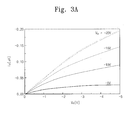
- FIG. 3A is a output curve of the organic thin film transistors in accordance with the embodiments of the present invention.
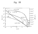
- FIG. 3B is a transfer curve of the organic thin film transistors in accordance with embodiments of the present invention.
- any material layer such as a conductive layer, a semiconductor layer, or an insulating layer is referred to as being 'on' another film or substrate, it can be directly on the other film or substrate, or intervening layers may also be present.
- the regions and the materials are not limited to these terms. These terms are used only to discriminate one region from another region. Therefore, a region referred to as a first region in one embodiment can be referred to as a second region in another embodiment.
- the composition may include an organic material with an anthracenyl group.
- the organic insulating material may be represented by Chemical Formula (I) or (II) :
- R' and R" each may be one selected from a hydrogen atom, a hydroxyl group, an ester group, an amide group, and an alkyl group or alkoxy group having 1 to 12 carbon atoms, and in Chemical Formula (I), n may be any positive integer.
- n and m may be any positive integer and the ratio of m to n (m/n) may be more than 0 and less than or equal to 99.
- the composition may also include a cross-linker with a maleimide group.
- the cross-linker with a maleimide group may be represented by one of the following Chemical Formulas (III), (IV), (V), or (VI):
- n may be any integer of 1 to 10.
- the composition may further include an organic solvent.
- An organic insulating film may be formed by using the composition.
- At least one selected from the organic materials and at least one selected from cross-linkers may be mixed with the solvent.
- a mixture thus formed may be coated on a substrate.
- a coating layer formed on the substrate may be subjected to a heat treatment. By the heat treatment, a Diels-Alder reaction may occur between an anthracenyl group of the organic material and a maleimide group of the cross-linker. The solvent in the coating layer may be removed. Thus, a cross-linked organic insulating layer may be formed on the substrate.
- n when n is more than 10 in Chemical Formulas (III), (IV), (V), or (VI) as a cross-linker, free space between the polymer chains formed may be enlarged, thereby deteriorating the insulation characteristics of the organic insulating layer.
- n may be 10 or less.
- the degree of crosslinking of the organic insulating layer may be controlled by the number of the maleimide functional groups included in Chemical Formulas (III), (IV), (V), or (VI) as a cross-linker.
- the mixing ratio of the cross-linker may be controlled in consideration of the number of the anthracenyl groups of the organic material.
- the degree of crosslinking may be low when the cross-linker is present at about 10 parts by weight per hundred (based on the weight of the organic material as 100), and the cross-linker may remain after reaction when the cross-linker is present at more than about 100 parts by weight. This can deteriorate the insulation characteristics of the formed organic insulating layer.
- the mixing ratio of the cross-linker may be about 10 to about 100 parts by weight.
- the composition including the organic material and the cross-linker may be mixed with the organic solvent at about 1 wt% to about 30 wt%, in consideration of its coatability.
- the organic solvent may be dichloroethane or trichloroethylene.
- the coating method of the mixture may be spin coating, drop casting, inkjet printing, and the like. Other direct printing methods may be used.
- a heat treatment may be performed at normal pressure, and at 95°C - 110°C for cross-linkage.
- the cross-linkage occurs at relatively low temperatures without any additional process (for example, UV irradiation).
- the 1,1'-(Methylenedi-4,1-phenylene)bis-maleimide was added in the same weight ratio (for example, 1:1) in relation to the content of the poly((methylmethacrylate)-co-(2-anthracenylmethyl acrylate) mixed with the solution.
- the solution including the 1,1'-(Methylenedi-4,1-phenylene)bis-maleimide and the poly((methylmethacrylate)-co-(2-anthracenylmethyl acrylate) was stirred enough to dissolve the materials in the solvent. After the materials were completely dissolved in the solvent, the solvent was filtered using a Teflon syringe filter in order to remove particles which remain in the solution.
- the solution was coated on the substrate to form a coating layer.
- the coating layer was formed by spin coating, and coated at 2000 rpm for 1 min. Subsequently, the coating layer was subjected to a heat treatment. The heat treatment was performed at 100°C for 10 minutes at normal pressure using a hot plate. By the heat treatment, cross-linking reactions occurred with the solution being removed in the coating layer. Thus, an organic insulating layer was formed on the substrate.
- the thickness of the organic insulating layer was about 150nm. At this time, the thickness of the organic insulating layer was measured by a step-profiler.
- the thickness of the organic insulating layer can be controlled by the concentration of the organic material including anthracenyl groups. For example, about 1 wt% poly((methylmethacrylate)-co-(2-anthracenylmethyl acrylate) was used to form an organic insulating layer with a thickness of about 70 - 100 nm and about 0.5 wt% poly((methylmethacrylate)-co-(2-anthracenylmethyl acrylate) was used to form an organic insulating layer with a thickness of 50 - 70 nm.
- a comparative sample (C1) was prepared to be compared with the samples.
- a coating layer was formed on a substrate by the same process as the manufacturing process of the samples. However, a heat treatment was not performed on the coating layer.
- an organic insulating layer was identified in the exemplary embodiment.
- the samples were prepared at different heat treatment temperatures, respectively. For example, a first sample (S1) was subjected to a heat treatment at 90°C and prepared, a second sample (S2) was subjected to a heat treatment at 100°C and prepared, a third sample was subjected to a heat treatment at 110°C and prepared, a fourth sample was subjected to a heat treatment at 120°C and prepared, and a fifth sample was subjected to a heat treatment at 130°C and prepared.
- S1 was subjected to a heat treatment at 90°C and prepared
- S2 was subjected to a heat treatment at 100°C and prepared
- a third sample was subjected to a heat treatment at 110°C and prepared
- a fourth sample was subjected to a heat treatment at 120°C and prepared
- a fifth sample was subjected to a heat treatment at 130°C and prepared.
- the UV-VIS absorbances of the comparative sample (C1) and the first to the fifth samples (S1 ⁇ S5) were measured.
- the coating layer of the comparative sample (C1) includes compositions which do not form a cross linkage.
- the absorption peak of an unreacted anthracenyl group can be shown.
- the comparative sample (C1) showed three absorption peaks in the range of 350 nm to 400 nm (for example, at 350 nm, 370 nm, and 390 nm). That is, any cross-linking reaction did not occur between anthracenyl group and maleimide group included in the composition used in formation of the comparative sample (C1).
- the samples (S1 ⁇ S5) did not show any absorption peak. That is, the samples (S1 ⁇ S5) did not include any unreacted and remaining anthracenyl group.
- the samples (S1 ⁇ S5) a formation of organic insulating layers cross-linked by a Diels-Alder reaction between anthracenyl group and maleimide group was identified.
- the first sample (S1) was treated at low temperatures of 100°C or less, the sample included an organic insulating layer formed by a cross-linking reaction between anthracenyl group and maleimide group.
- organic thin film transistors including an organic insulating layer formed by the composition and a method for manufacturing the same will be described below.
- the organic thin film transistor includes a substrate, a gate electrode, a gate insulating layer, an organic active layer, and source/drain electrodes. At this time, the organic insulating layer is used as the gate insulating layer.
- a source electrode 120 and a drain electrode 130 are formed to be disposed spaced apart on a substrate 110.
- An organic active layer 140 may be formed on the substrate 110.
- the organic active layer 140 may cover the source electrode 120 and the drain electrode 130.
- a gate insulating layer 150 may be formed on the organic active layer 140.
- a gate electrode 160 may be formed to be disposed on the gate insulating layer 150 between the source electrode 120 and the drain electrode 130.
- a gate electrode 160 may be formed on a substrate 110.
- a gate insulating layer 150 may be formed on the substrate 110 to cover the gate electrode 160.
- a source electrode 120 and a drain electrode 130 may be formed on the gate insulating layer 150 to be spaced apart the gate electrode 160.
- An organic active layer 140 may be stacked on the gate insulating layer 150 to cover the source electrode 120 and the drain electrode 130.
- a gate electrode 160 may be formed on a substrate 110.
- a gate insulating layer 150 may be formed on the substrate 110 to cover the gate electrode 160.
- An organic active layer 140 may be stacked on the gate insulating layer 150.
- a source electrode 120 and a drain electrode 130 may be formed on the organic active layer 140 to be spaced apart the gate electrode 160.
- the substrate 110 may be a n- type or p-type doped silicon wafer.
- the substrate 110 may be a glass substrate.
- the substrate 110 may be a plastic film including at least one material selected from the group consisting of polyethersulphone, polyacrylate, polyetherimide, polyimide, and polyethyleneterephtalate.
- the substrate 110 may include an indium tin oxide coated on the surface.
- the gate electrode 160 and the source/drain electrodes 120 and 130 may include a metal or a conductive polymer.
- the gate electrode 160 and the source/drain electrodes 120 and 130 may include Au, Ag, Al, Ni, and/or indium tin oxide (ITO).
- the gate electrode 160 and the source/drain electrodes 120 and 130 may include polyethylenedioxythiophene : polystyrene sulfonate (PEDOT : PSS), polypyrrole, and/or polyaniline.
- the source/drain electrodes 120 and 130 may be formed by a vapor deposition process and a photolithography process or an inkjet printing technique.
- the gate electrode 160 may be formed by a vapor deposition process using a shadow mask, or an inkjet printing technique.
- the organic active layer 140 may include polythiophene, thieno thiophene, triisopropylsilyl pentacene, pentacene precursor, polyfluorene, pentacene, tetracene, anthracene, perylene, rubrene, coronene, perylene tetracarboxylic diimide, polyparaphenylene vinylene, polythiophene vinylene, oligothiophene such as ⁇ -5-thiophene or ⁇ -6-thiophene, phthalocyanine containing or not containing a metal, and/or naphthalene tetra carboxylic acid diimide, and/or derivatives thereof.
- the organic active layer 140 may be formed by a solution process such as spin coating or inkjet printing.
- the gate insulating layer 150 may be an organic insulating layer formed by a cross-linkage between anthracenyl group and maleimide group.
- the organic insulating layer has a solvent resistance to organic solvents after a cross-linking reaction.
- another thin film may be formed by a solution process on the organic insulating layer, as described in the manufacturing method.
- top gated organic thin film transistors formed by exemplary embodiments of the manufacturing method are described.
- a Eagle 2000 glass slide was used for a substrate, gold electrodes were used as source/drain electrodes, and gold or aluminum electrode was used as a gate electrode.
- Poly(9,9-dioctylfluorene-co-bithiophene) (F8T2) was used as an organic active layer.
- An organic insulating layer formed by a cross-linkage between anthracenyl group and maleimide group was used as a gate insulating layer, and the thickness of the gate insulating layer was 150 nm .
- the drain current (Id) was measured by varying the drain voltage (Vd). Although the gate voltage and the drain voltage were increased, the drain current was stably measured, thereby confirming the physical stability of an organic insulating layer used in the organic thin film transistors.
- the drain current (Id) and the gate leakage current (Ig) were measured by varying the gate voltage (Vg).
- the values of the gate leakage current (Ig) are shown on left Y axis in log scale. Referring to FIG. 3b , the leakage current density was 1nA/cm 2 or less when a gate voltage of -20V and a drain voltage of -20V were supplied.
- a threshold voltage of the organic thin film transistor was calculated by using the measured drain current (Id).
- the threshold voltage of the organic thin film transistor was -1V.
- the threshold voltage was calculated by using a contact point at which a graph curve showing the root values of the drain current Id meets at x-axis. According to the graph, the organic thin film transistor in the embodiment showed a charge mobility of about 5 x 10 -3 cm 2 /Vs limited to amorphous semiconducting polymer F8T2.
- composition in accordance with embodiments of the present invention can be cross-linked at low temperatures of 100°C or less.
- a cross-linked organic insulating layer can have solvent resistance to other organic solvents. Also, the organic insulating layer may have a durability which high voltages can be endured in thin thicknesses. Because the organic insulating layer can be formed in thin thicknesses, organic thin film transistors including the organic insulating layer can be operated at low threshold voltages. Furthermore, the organic insulating layer has excellent insulation characteristics, which can lead to a reduction in leakage voltage.
- the manufacturing method in embodiments of the present invention can be performed at low processing temperatures less than 100 °C, processing burdens can be reduced and very suitable for top gated geometry.
Landscapes
- Chemical & Material Sciences (AREA)
- Health & Medical Sciences (AREA)
- Chemical Kinetics & Catalysis (AREA)
- Medicinal Chemistry (AREA)
- Polymers & Plastics (AREA)
- Organic Chemistry (AREA)
- General Chemical & Material Sciences (AREA)
- Engineering & Computer Science (AREA)
- Materials Engineering (AREA)
- Thin Film Transistor (AREA)
Abstract
Provided are a composition for organic thin film transistors including a material including an anthracenyl group and a cross-linker including a maleimide group, an organic thin film transistor formed by using the composition, and a method for manufacturing the same.
Description
- This patent application claims priority of Korean Patent Application No.
10-2008-0107801, filed on October 31, 2008 - The present invention disclosed herein relates to a composition for organic thin film transistors, an organic thin film transistor formed by using the composition, and a method for forming the organic thin film transistors by using the composition.
- Organic thin film transistors (OTFTs) can be applied in various flexible electronic devices such as driving devices for the next generation flexible displays (or a logic circuit of extremely low priced Radio Frequency Identification (RFID) tags for individual item unit identification). Thus, recent studies on OTFTs have been actively conducted.
- In the OTFT manufacturing process, polymer materials can be provided as a solution, and thus used in roll to roll processes. Therefore, a manufacturing process using polymer materials can be performed at lower manufacturing costs than typical transistor manufacturing processes.
- The present invention provides a composition for organic insulating layers having excellent electrical characteristics.
- The present invention also provides organic thin film transistors including organic insulating layers having excellent electrical characteristics.
- The present invention also provides a method for manufacturing organic thin film transistors including organic insulating layers manufactured by simple processes, but having excellent electrical characteristics.
- Embodiments of the present invention provide compositions for organic thin film transistors, including a material represented by Chemical Formula I or II and a cross-linker with a maleimide group


- In some embodiments, the cross-linker with a maleimide group may be one selected from Chemical Formulas III, IV, V, and VI:


- In other embodiments, the amount of the cross-linker may be 10 to 100 parts by weight in 100 parts by weight of the material.
- In still other embodiments, the composition may further include an organic solvent.
- In other embodiments of the present invention, organic thin film transistors include an organic insulating layer formed by a cross-linkage between a material represented by Chemical Formula I or II and a cross-linker with a maleimide group.


- In some embodiments, the organic insulating layer may be formed on a substrate, and the organic thin film transistor may further comprise a source electrode, a drain electrode, an organic insulating layer, and a gate electrode.
- In still other embodiments of the present invention, methods for forming organic thin film transistors include preparing a solution containing a material represented by Chemical Formula I or II and a cross-linker with a maleimide group, coating the solution on a substrate; and subjecting the coated substrate to a heat treatment to form an organic insulating layer on the substrate.


- In some embodiments, by the heat treatment, a Diels-Alder reaction occurs between the material and the cross-linker.
- In other embodiments, the method may further include forming a gate electrode on the substrate prior to the coating of the solution; and forming an organic active layer on the organic insulating layer and forming a source and a drain after the forming of the organic insulating layer.
- In still other embodiments, the method may further include forming a source and a drain on the substrate and forming an organic active layer on the substrate prior to the coating of the solution; and forming a gate electrode on the organic insulating layer after the forming of the organic insulating layer.
- The accompanying figures are included to provide a further understanding of the present invention, and are incorporated in and constitute a part of this specification. The drawings illustrate exemplary embodiments of the present invention and, together with the description, serve to explain principles of the present invention. In the figures:
-
FIG. 1 is a graph showing UV absorbance of the organic insulating layer in accordance with embodiments of the present invention and UV absorbance of the coating layer in accordance with a comparative embodiment of the present invention; -
FIGS. 2A through 2C are schematic views showing an organic thin film transistor in accordance with embodiments of the present invention; -
FIG. 3A is a output curve of the organic thin film transistors in accordance with the embodiments of the present invention; and -
FIG. 3B is a transfer curve of the organic thin film transistors in accordance with embodiments of the present invention. - Embodiments of the present invention will be described below in more detail with reference to the accompanying drawings. The present invention may, however, be embodied in different forms and should not be construed as limited to the embodiments set forth herein. Rather, these embodiments are provided so that this disclosure will be thorough and complete, and will fully convey the scope of the present invention to those skilled in the art. In the drawings, like reference numerals were used together for referring to like elements with like functions.
- In the specification, it will be understood that when any material layer such as a conductive layer, a semiconductor layer, or an insulating layer is referred to as being 'on' another film or substrate, it can be directly on the other film or substrate, or intervening layers may also be present. Also, though terms like a first, a second, and a third are used to describe various regions and materials in various embodiments of the present invention, the regions and the materials are not limited to these terms. These terms are used only to discriminate one region from another region. Therefore, a region referred to as a first region in one embodiment can be referred to as a second region in another embodiment.
- In the specification, it should be understood that the term 'and/or' refers to one or all of the listed elements before and after the term.
- According to embodiments of the present invention, a composition for organic thin film transistors will be described.
- The composition may include an organic material with an anthracenyl group. For example, the organic insulating material may be represented by Chemical Formula (I) or (II) :


- In Chemical Formula (I) or Chemical Formula (II), R' and R" each may be one selected from a hydrogen atom, a hydroxyl group, an ester group, an amide group, and an alkyl group or alkoxy group having 1 to 12 carbon atoms, and in Chemical Formula (I), n may be any positive integer. In Chemical Formula (II), n and m may be any positive integer and the ratio of m to n (m/n) may be more than 0 and less than or equal to 99.
- For example, n and m in Chemical Formula (II) may be expressed in a ratio form (eg, n:m=a:b). Then, the sum of a and b is 1, a may be any real number which is more than or equal to 0.01 and less than 1 and b may be any real number which is more than 0 and less than or equal to 0.99.
- The composition may also include a cross-linker with a maleimide group. The cross-linker with a maleimide group may be represented by one of the following Chemical Formulas (III), (IV), (V), or (VI):


- In Chemical Formulas (III), (IV), (V), or (VI), n may be any integer of 1 to 10.
- The composition may further include an organic solvent.
- An organic insulating film may be formed by using the composition.
- At least one selected from the organic materials and at least one selected from cross-linkers may be mixed with the solvent. A mixture thus formed may be coated on a substrate. A coating layer formed on the substrate may be subjected to a heat treatment. By the heat treatment, a Diels-Alder reaction may occur between an anthracenyl group of the organic material and a maleimide group of the cross-linker. The solvent in the coating layer may be removed. Thus, a cross-linked organic insulating layer may be formed on the substrate.
- Then, when n is more than 10 in Chemical Formulas (III), (IV), (V), or (VI) as a cross-linker, free space between the polymer chains formed may be enlarged, thereby deteriorating the insulation characteristics of the organic insulating layer. Thus, n may be 10 or less. The degree of crosslinking of the organic insulating layer may be controlled by the number of the maleimide functional groups included in Chemical Formulas (III), (IV), (V), or (VI) as a cross-linker.
- In the composition, the mixing ratio of the cross-linker may be controlled in consideration of the number of the anthracenyl groups of the organic material. The degree of crosslinking may be low when the cross-linker is present at about 10 parts by weight per hundred (based on the weight of the organic material as 100), and the cross-linker may remain after reaction when the cross-linker is present at more than about 100 parts by weight. This can deteriorate the insulation characteristics of the formed organic insulating layer. Thus, the mixing ratio of the cross-linker may be about 10 to about 100 parts by weight.
- The composition including the organic material and the cross-linker may be mixed with the organic solvent at about 1 wt% to about 30 wt%, in consideration of its coatability. The organic solvent may be dichloroethane or trichloroethylene.
- The coating method of the mixture may be spin coating, drop casting, inkjet printing, and the like. Other direct printing methods may be used.
- A heat treatment may be performed at normal pressure, and at 95°C - 110°C for cross-linkage. The cross-linkage occurs at relatively low temperatures without any additional process (for example, UV irradiation).
- Hereinafter, a method for forming an organic insulating layer and whether the organic insulating layer can be formed will be described in accordance with exemplary embodiments.
- 3 wt% (of a solvent) poly((methylmethacrylate)-co-(2-anthracenylmethyl acrylate)) (Sigma Aldrich) including a anthracenyl group as a side branch was dissolved in the solvent to prepare a solution. At this time, dichloroethane was used as a solvent. 1,1'-(Methylenedi-4,1-phenylene)bismaleimide (Sigma Aldrich) was mixed as a cross-linker with the solution. At this time, the 1,1'-(Methylenedi-4,1-phenylene)bis-maleimide was added in the same weight ratio (for example, 1:1) in relation to the content of the poly((methylmethacrylate)-co-(2-anthracenylmethyl acrylate) mixed with the solution.
- Subsequently, the solution including the 1,1'-(Methylenedi-4,1-phenylene)bis-maleimide and the poly((methylmethacrylate)-co-(2-anthracenylmethyl acrylate) was stirred enough to dissolve the materials in the solvent. After the materials were completely dissolved in the solvent, the solvent was filtered using a Teflon syringe filter in order to remove particles which remain in the solution.
- The solution was coated on the substrate to form a coating layer. The coating layer was formed by spin coating, and coated at 2000 rpm for 1 min. Subsequently, the coating layer was subjected to a heat treatment. The heat treatment was performed at 100°C for 10 minutes at normal pressure using a hot plate. By the heat treatment, cross-linking reactions occurred with the solution being removed in the coating layer. Thus, an organic insulating layer was formed on the substrate.
- The thickness of the organic insulating layer was about 150nm. At this time, the thickness of the organic insulating layer was measured by a step-profiler. The thickness of the organic insulating layer can be controlled by the concentration of the organic material including anthracenyl groups. For example, about 1 wt% poly((methylmethacrylate)-co-(2-anthracenylmethyl acrylate) was used to form an organic insulating layer with a thickness of about 70 - 100 nm and about 0.5 wt% poly((methylmethacrylate)-co-(2-anthracenylmethyl acrylate) was used to form an organic insulating layer with a thickness of 50 - 70 nm.
- By the process, organic insulating layer samples were prepared.
- A comparative sample (C1) was prepared to be compared with the samples. To prepare the comparative sample (C1), a coating layer was formed on a substrate by the same process as the manufacturing process of the samples. However, a heat treatment was not performed on the coating layer.
- Referring to
FIG. 1 , the formation of an organic insulating layer was identified in the exemplary embodiment. - The samples were prepared at different heat treatment temperatures, respectively. For example, a first sample (S1) was subjected to a heat treatment at 90°C and prepared, a second sample (S2) was subjected to a heat treatment at 100°C and prepared, a third sample was subjected to a heat treatment at 110°C and prepared, a fourth sample was subjected to a heat treatment at 120°C and prepared, and a fifth sample was subjected to a heat treatment at 130°C and prepared.
- The UV-VIS absorbances of the comparative sample (C1) and the first to the fifth samples (S1∼S5) were measured.
- The coating layer of the comparative sample (C1) includes compositions which do not form a cross linkage. Thus, the absorption peak of an unreacted anthracenyl group can be shown. Referring to
FIG. 1 , the comparative sample (C1) showed three absorption peaks in the range of 350 nm to 400 nm (for example, at 350 nm, 370 nm, and 390 nm). That is, any cross-linking reaction did not occur between anthracenyl group and maleimide group included in the composition used in formation of the comparative sample (C1). - On the contrary, the samples (S1∼S5) did not show any absorption peak. That is, the samples (S1∼S5) did not include any unreacted and remaining anthracenyl group. Thus, in the samples (S1∼S5), a formation of organic insulating layers cross-linked by a Diels-Alder reaction between anthracenyl group and maleimide group was identified. Furthermore, although the first sample (S1) was treated at low temperatures of 100°C or less, the sample included an organic insulating layer formed by a cross-linking reaction between anthracenyl group and maleimide group.
- Referring to
FIGS. 2a through 2c , organic thin film transistors including an organic insulating layer formed by the composition and a method for manufacturing the same will be described below. - The organic thin film transistor includes a substrate, a gate electrode, a gate insulating layer, an organic active layer, and source/drain electrodes. At this time, the organic insulating layer is used as the gate insulating layer.
- Referring to
FIG. 2a , asource electrode 120 and adrain electrode 130 are formed to be disposed spaced apart on asubstrate 110. An organicactive layer 140 may be formed on thesubstrate 110. The organicactive layer 140 may cover thesource electrode 120 and thedrain electrode 130. Agate insulating layer 150 may be formed on the organicactive layer 140. Agate electrode 160 may be formed to be disposed on thegate insulating layer 150 between thesource electrode 120 and thedrain electrode 130. - Referring to
FIG. 2b , agate electrode 160 may be formed on asubstrate 110. Agate insulating layer 150 may be formed on thesubstrate 110 to cover thegate electrode 160. Asource electrode 120 and adrain electrode 130 may be formed on thegate insulating layer 150 to be spaced apart thegate electrode 160. An organicactive layer 140 may be stacked on thegate insulating layer 150 to cover thesource electrode 120 and thedrain electrode 130. - Referring to
FIG. 2c , agate electrode 160 may be formed on asubstrate 110. Agate insulating layer 150 may be formed on thesubstrate 110 to cover thegate electrode 160. An organicactive layer 140 may be stacked on thegate insulating layer 150. Asource electrode 120 and adrain electrode 130 may be formed on the organicactive layer 140 to be spaced apart thegate electrode 160. - In
FIGS. 2a through 2c , thesubstrate 110 may be a n- type or p-type doped silicon wafer. Alternatively, thesubstrate 110 may be a glass substrate. Alternatively, thesubstrate 110 may be a plastic film including at least one material selected from the group consisting of polyethersulphone, polyacrylate, polyetherimide, polyimide, and polyethyleneterephtalate. Thesubstrate 110 may include an indium tin oxide coated on the surface. - The
gate electrode 160 and the source/drain electrodes gate electrode 160 and the source/drain electrodes gate electrode 160 and the source/drain electrodes drain electrodes gate electrode 160 may be formed by a vapor deposition process using a shadow mask, or an inkjet printing technique. - The organic
active layer 140 may include polythiophene, thieno thiophene, triisopropylsilyl pentacene, pentacene precursor, polyfluorene, pentacene, tetracene, anthracene, perylene, rubrene, coronene, perylene tetracarboxylic diimide, polyparaphenylene vinylene, polythiophene vinylene, oligothiophene such as α -5-thiophene or α -6-thiophene, phthalocyanine containing or not containing a metal, and/or naphthalene tetra carboxylic acid diimide, and/or derivatives thereof. The organicactive layer 140 may be formed by a solution process such as spin coating or inkjet printing. - As described above in the method, the
gate insulating layer 150 may be an organic insulating layer formed by a cross-linkage between anthracenyl group and maleimide group. The organic insulating layer has a solvent resistance to organic solvents after a cross-linking reaction. Thus, another thin film may be formed by a solution process on the organic insulating layer, as described in the manufacturing method. - Referring to
FIGS. 3a and3b , electrical characteristics of top gated organic thin film transistors formed by exemplary embodiments of the manufacturing method are described. - A Eagle 2000 glass slide was used for a substrate, gold electrodes were used as source/drain electrodes, and gold or aluminum electrode was used as a gate electrode. Poly(9,9-dioctylfluorene-co-bithiophene) (F8T2) was used as an organic active layer. An organic insulating layer formed by a cross-linkage between anthracenyl group and maleimide group was used as a gate insulating layer, and the thickness of the gate insulating layer was 150 nm .
- Referring to
FIG. 3a , an output curve of the organic thin film transistor is described. - When a gate voltage (Vg) was applied at -5V, -10V, -15V, and -20V, the drain current (Id) was measured by varying the drain voltage (Vd). Although the gate voltage and the drain voltage were increased, the drain current was stably measured, thereby confirming the physical stability of an organic insulating layer used in the organic thin film transistors.
- Referring to
FIG. 3b , a transfer curve of the organic thin film transistor is described. - When a drain voltage (Vd) was applied at -5V and -20V, the drain current (Id) and the gate leakage current (Ig) were measured by varying the gate voltage (Vg). The values of the gate leakage current (Ig) are shown on left Y axis in log scale. Referring to
FIG. 3b , the leakage current density was 1nA/cm2 or less when a gate voltage of -20V and a drain voltage of -20V were supplied. - In addition, a threshold voltage of the organic thin film transistor was calculated by using the measured drain current (Id). The threshold voltage of the organic thin film transistor was -1V. The threshold voltage was calculated by using a contact point at which a graph curve showing the root values of the drain current

- The composition in accordance with embodiments of the present invention can be cross-linked at low temperatures of 100°C or less.
- A cross-linked organic insulating layer can have solvent resistance to other organic solvents. Also, the organic insulating layer may have a durability which high voltages can be endured in thin thicknesses. Because the organic insulating layer can be formed in thin thicknesses, organic thin film transistors including the organic insulating layer can be operated at low threshold voltages. Furthermore, the organic insulating layer has excellent insulation characteristics, which can lead to a reduction in leakage voltage.
- Because the manufacturing method in embodiments of the present invention can be performed at low processing temperatures less than 100 °C, processing burdens can be reduced and very suitable for top gated geometry.
- The above-disclosed subject matter is to be considered illustrative, and not restrictive, and the appended claims are intended to cover all such modifications, enhancements, and other embodiments, which fall within the true spirit and scope of the present invention. Thus, to the maximum extent allowed by law, the scope of the present invention is to be determined by the broadest permissible interpretation of the following claims and their equivalents, and shall not be restricted or limited by the foregoing detailed description.
Claims (10)
- A composition for organic thin film transistor, comprising:a material represented by Chemical Formula I or II; anda cross-linker with a maleimide groupwherein each of R' and R" in Chemical Formula I or II is one selected from a hydrogen atom, a hydroxyl group, an ester group, an amide group, and an alkyl groups or an alkoxy group having 1 to 12 carbon numbers,


n in Chemical Formula I is a positive integer, and
n and m are positive integers in Chemical Formula II and the ratio of m to n (m/n) is more than 0 and less than or equal to 99. - The composition of claim 1, wherein the cross-linker with a maleimide group is one selected from Chemical Formulas III, IV, V, and VI:


- The composition of claim 1 or 2, wherein the amount of the cross-linker is 10 to 100 parts by weight in 100 parts by weight of the material.
- The composition of any of claims 1 to 3, further comprising an organic solvent.
- An organic thin film transistor, comprising:an organic insulating layer formed by a cross-linkage between a material represented by Chemical Formula I or II and a cross-linker with a maleimide groupwherein Chemical Formula I or II, R' and R" each is one selected from a hydrogen atom, a hydroxyl group, an ester group, an amide group, and an alkyl group or an alkoxy group having 1 to 12 carbon numbers,


n in Chemical Formula I is a positive integer, and
n and m in Chemical Formula II are positive integers and the ratio of m to n (m/n) is more than 0 and less than or equal to 99. - The organic thin film transistor of claim 5, wherein the organic insulating layer is formed on a substrate, and further comprising a source electrode, a drain electrode, an organic insulating layer, and a gate electrode.
- A method for forming organic thin film transistors, comprising:preparing a solution containing a material represented by Chemical Formula I or II and a cross-linker with a maleimide group;coating the solution on a substrate; andsubjecting the coated substrate to a heat treatment to form an organic insulating layer on the substratewherein each of R' and R" in Chemical Formula I or II each is one selected from a hydrogen atom, a hydroxyl group, an ester group, an amide group, and an alkyl group or an alkoxy group having 1 to 12 carbon numbers,


n in Chemical Formula I is a positive integer, and
n and m in Chemical Formula II are positive integers and the ratio of m to n (m/n) is more than 0 and less than or equal to 99. - The method of claim 7, wherein by the heat treatment, a Diels-Alder reaction occurs between the material and the cross-linker.
- The method of claim 7 or 8, further comprising:forming a gate electrode on the substrate prior to the coating of the solution; andforming an organic active layer on the organic insulating layer and forming a source and a drain after the forming of the organic insulating layer.
- The method of any of claims 7 to 9, further comprising:forming a source and a drain on the substrate and forming an organic active layer on the substrate prior to the coating of the solution,; andforming a gate electrode on the organic insulating layer after the forming of the organic insulating layer.
Applications Claiming Priority (1)
| Application Number | Priority Date | Filing Date | Title |
|---|---|---|---|
| KR1020080107801A KR100975913B1 (en) | 2008-10-31 | 2008-10-31 | Composition for organic thin film transistor, organic thin film transistor formed using same and method for forming same |
Publications (1)
| Publication Number | Publication Date |
|---|---|
| EP2182012A1 true EP2182012A1 (en) | 2010-05-05 |
Family
ID=41259679
Family Applications (1)
| Application Number | Title | Priority Date | Filing Date |
|---|---|---|---|
| EP09167846A Withdrawn EP2182012A1 (en) | 2008-10-31 | 2009-08-13 | Composition for organic thin film transistor, organic thin film transistor formed by using the same, and method for forming the organic film transistor |
Country Status (3)
| Country | Link |
|---|---|
| US (1) | US7960724B2 (en) |
| EP (1) | EP2182012A1 (en) |
| KR (1) | KR100975913B1 (en) |
Families Citing this family (3)
| Publication number | Priority date | Publication date | Assignee | Title |
|---|---|---|---|---|
| ITMI20111447A1 (en) * | 2011-07-29 | 2013-01-30 | E T C Srl | ELECTROLUMINESCENT ORGANIC TRANSISTOR |
| WO2019002273A1 (en) | 2017-06-26 | 2019-01-03 | Solvay Specialty Polymers Usa, Llc | Aromatic polymers obtainable by cycloaddition reaction |
| GB2631234A (en) * | 2023-06-21 | 2025-01-01 | Flexenable Tech Limited | Compound |
Citations (1)
| Publication number | Priority date | Publication date | Assignee | Title |
|---|---|---|---|---|
| US20080067505A1 (en) * | 2006-09-15 | 2008-03-20 | Samsung Electronics Co., Ltd. | Composition for preparing organic insulating film, organic insulating film prepared by using the same and organic thin film transistor comprising the organic insulating film |
Family Cites Families (15)
| Publication number | Priority date | Publication date | Assignee | Title |
|---|---|---|---|---|
| US4711964A (en) | 1986-05-08 | 1987-12-08 | University Of Dayton | Bisdiene from bis-benzocyclobutene compound |
| US6215130B1 (en) * | 1998-08-20 | 2001-04-10 | Lucent Technologies Inc. | Thin film transistors |
| KR20000061889A (en) * | 1999-03-31 | 2000-10-25 | 윤종용 | Chemically amplified resist compounds comprising blending polymer composed of at least two anthracene derivative-containing photosensitive polymers |
| KR100395904B1 (en) * | 1999-04-23 | 2003-08-27 | 주식회사 하이닉스반도체 | Organic Anti-reflective coating material and its preparation |
| AU2002343058A1 (en) * | 2001-12-19 | 2003-06-30 | Merck Patent Gmbh | Organic field effect transistor with an organic dielectric |
| US7884355B2 (en) * | 2003-05-12 | 2011-02-08 | Cambridge Enterprise Ltd | Polymer transistor |
| KR20050058062A (en) | 2003-12-11 | 2005-06-16 | 삼성전자주식회사 | Composition for preparing organic insulating film and the organic insulating film prepared by using the same |
| EP1839339A2 (en) * | 2004-12-23 | 2007-10-03 | Northwestern University | Siloxane-polymer dielectric compositions and related organic field-effect transistors |
| KR100741072B1 (en) * | 2005-01-17 | 2007-07-19 | 삼성에스디아이 주식회사 | A thin film transistor, a method of manufacturing the same, and a flat panel display device having the thin film transistor |
| KR101139052B1 (en) * | 2005-12-06 | 2012-04-30 | 삼성전자주식회사 | Organic Insulator composition having Fluorine and Organic Semiconductor Thin Film using the Same |
| KR101186725B1 (en) * | 2006-02-21 | 2012-09-28 | 삼성전자주식회사 | Organic Thin Film Transistor Comprising Fluorine-based Polymer Thin Film and Method for Fabricating the Same |
| US7853509B2 (en) * | 2006-03-23 | 2010-12-14 | Hartford Fire Insurance Company | Lifetime income |
| KR20080011879A (en) | 2006-08-01 | 2008-02-11 | 동우 화인켐 주식회사 | Photosensitive organic insulating film composition and organic insulating film prepared using the same |
| KR101151106B1 (en) * | 2006-09-15 | 2012-06-01 | 삼성전자주식회사 | Organic Insulating Polymer and Organic Insulating Layer and Organic Thin Film Transistor Prepared by using the Same |
| KR101258294B1 (en) | 2006-11-13 | 2013-04-25 | 삼성전자주식회사 | Composition for Preparing Organic Insulator with Crosslinking Property and the Organic Insulator Prepared by using the same |
-
2008
- 2008-10-31 KR KR1020080107801A patent/KR100975913B1/en not_active Expired - Fee Related
-
2009
- 2009-08-13 EP EP09167846A patent/EP2182012A1/en not_active Withdrawn
- 2009-08-17 US US12/542,226 patent/US7960724B2/en not_active Expired - Fee Related
Patent Citations (1)
| Publication number | Priority date | Publication date | Assignee | Title |
|---|---|---|---|---|
| US20080067505A1 (en) * | 2006-09-15 | 2008-03-20 | Samsung Electronics Co., Ltd. | Composition for preparing organic insulating film, organic insulating film prepared by using the same and organic thin film transistor comprising the organic insulating film |
Non-Patent Citations (2)
| Title |
|---|
| DE DEUS ET AL: "Nanomechanical properties of poly(methyl methacrylate-co-9-anthryl methyl methacrylate)", SURFACE AND COATINGS TECHNOLOGY, ELSEVIER, AMSTERDAM, NL, vol. 201, no. 6, 17 November 2006 (2006-11-17), pages 3615 - 3620, XP005729331, ISSN: 0257-8972 * |
| TAE-DONG K. ET AL.: "Diels-Alder "Click Chemistry" for Highly Efficient Electrooptic Polymers", MACROMOLECULES, vol. 39, no. 5, 2 February 2006 (2006-02-02), pages 1676 - 1680, XP002555835 * |
Also Published As
| Publication number | Publication date |
|---|---|
| KR20100048576A (en) | 2010-05-11 |
| US20100108996A1 (en) | 2010-05-06 |
| US7960724B2 (en) | 2011-06-14 |
| KR100975913B1 (en) | 2010-08-13 |
Similar Documents
| Publication | Publication Date | Title |
|---|---|---|
| TWI460897B (en) | Method of preparing an electronic device | |
| Kim et al. | Printable cross-linked polymer blend dielectrics. Design strategies, synthesis, microstructures, and electrical properties, with organic field-effect transistors as testbeds | |
| US7834352B2 (en) | Method of fabricating thin film transistor | |
| US9929345B1 (en) | Curable polymeric materials and their use for fabricating electronic devices | |
| US8748873B2 (en) | Electronic device with dual semiconducting layer | |
| US8202759B2 (en) | Manufacturing method of organic semiconductor device | |
| KR20130112882A (en) | Process for preparing an organic electronic device | |
| US8319206B2 (en) | Thin film transistors comprising surface modified carbon nanotubes | |
| KR20160112030A (en) | Thin-film transistor having dual gate electrode | |
| JP2009260346A (en) | Organic thin film transistor | |
| US20100140596A1 (en) | Organic thin film transistor and method of manufacturing the same | |
| US11345778B2 (en) | Organic dielectric materials and devices including them | |
| US20080070343A1 (en) | Methods for forming an organic thin film using solvent effects, organic thin film formed by the method, and organic electronic device comprising organic thin film | |
| US7960724B2 (en) | Composition for organic thin film transistor, organic thin film transistor formed by using the same, and method for forming the organic film transistor | |
| JP2006295165A (en) | Thin film transistor and method for manufacturing thin film transistor | |
| US7863694B2 (en) | Organic thin film transistors | |
| US20200266353A1 (en) | Organic thin film transistor, and fabricating method thereof | |
| JP6062182B2 (en) | Organic thin film transistor | |
| US10147895B2 (en) | Curable polymeric materials and their use for fabricating electronic devices | |
| JP2010045327A (en) | Method of locally crystallizing organic thin film and method of manufacturing organic thin-film transistor using the same | |
| Sangwan et al. | Modulating poly (methyl methacrylate) gate dielectric behavior with cosolvent and low-temperature processing for low-threshold-voltage flexible organic field-effect transistors | |
| KR101113166B1 (en) | Organic phototransistor | |
| KR20140036665A (en) | Organic thin film transistor and method of manufacturing the same | |
| KR101140686B1 (en) | Composition for Organic Gate Insulating Film And Organic Gate Insulating Film Prepared by using the same | |
| Zhao et al. | Toward Flexible Low‐Voltage Complementary Circuits with Solution‐Deposited Organic Semiconductor Single‐Crystal Films |
Legal Events
| Date | Code | Title | Description |
|---|---|---|---|
| PUAI | Public reference made under article 153(3) epc to a published international application that has entered the european phase |
Free format text: ORIGINAL CODE: 0009012 |
|
| AK | Designated contracting states |
Kind code of ref document: A1 Designated state(s): AT BE BG CH CY CZ DE DK EE ES FI FR GB GR HR HU IE IS IT LI LT LU LV MC MK MT NL NO PL PT RO SE SI SK SM TR |
|
| 17P | Request for examination filed |
Effective date: 20101105 |
|
| 17Q | First examination report despatched |
Effective date: 20140710 |
|
| STAA | Information on the status of an ep patent application or granted ep patent |
Free format text: STATUS: THE APPLICATION IS DEEMED TO BE WITHDRAWN |
|
| 18D | Application deemed to be withdrawn |
Effective date: 20141121 |