EP2180505A2 - Wafer-level fabrication of a package with stud bumps coated with solder - Google Patents
Wafer-level fabrication of a package with stud bumps coated with solder Download PDFInfo
- Publication number
- EP2180505A2 EP2180505A2 EP20090252154 EP09252154A EP2180505A2 EP 2180505 A2 EP2180505 A2 EP 2180505A2 EP 20090252154 EP20090252154 EP 20090252154 EP 09252154 A EP09252154 A EP 09252154A EP 2180505 A2 EP2180505 A2 EP 2180505A2
- Authority
- EP
- European Patent Office
- Prior art keywords
- stud bumps
- wire
- wafer
- stud
- capillary
- Prior art date
- Legal status (The legal status is an assumption and is not a legal conclusion. Google has not performed a legal analysis and makes no representation as to the accuracy of the status listed.)
- Withdrawn
Links
Images


Classifications
-
- H—ELECTRICITY
- H01—ELECTRIC ELEMENTS
- H01L—SEMICONDUCTOR DEVICES NOT COVERED BY CLASS H10
- H01L21/00—Processes or apparatus adapted for the manufacture or treatment of semiconductor or solid state devices or of parts thereof
- H01L21/02—Manufacture or treatment of semiconductor devices or of parts thereof
- H01L21/04—Manufacture or treatment of semiconductor devices or of parts thereof the devices having at least one potential-jump barrier or surface barrier, e.g. PN junction, depletion layer or carrier concentration layer
- H01L21/50—Assembly of semiconductor devices using processes or apparatus not provided for in a single one of the subgroups H01L21/06 - H01L21/326, e.g. sealing of a cap to a base of a container
- H01L21/56—Encapsulations, e.g. encapsulation layers, coatings
- H01L21/561—Batch processing
-
- H—ELECTRICITY
- H01—ELECTRIC ELEMENTS
- H01L—SEMICONDUCTOR DEVICES NOT COVERED BY CLASS H10
- H01L24/00—Arrangements for connecting or disconnecting semiconductor or solid-state bodies; Methods or apparatus related thereto
- H01L24/01—Means for bonding being attached to, or being formed on, the surface to be connected, e.g. chip-to-package, die-attach, "first-level" interconnects; Manufacturing methods related thereto
- H01L24/02—Bonding areas ; Manufacturing methods related thereto
- H01L24/04—Structure, shape, material or disposition of the bonding areas prior to the connecting process
- H01L24/05—Structure, shape, material or disposition of the bonding areas prior to the connecting process of an individual bonding area
-
- H—ELECTRICITY
- H01—ELECTRIC ELEMENTS
- H01L—SEMICONDUCTOR DEVICES NOT COVERED BY CLASS H10
- H01L24/00—Arrangements for connecting or disconnecting semiconductor or solid-state bodies; Methods or apparatus related thereto
- H01L24/01—Means for bonding being attached to, or being formed on, the surface to be connected, e.g. chip-to-package, die-attach, "first-level" interconnects; Manufacturing methods related thereto
- H01L24/10—Bump connectors ; Manufacturing methods related thereto
- H01L24/11—Manufacturing methods
-
- H—ELECTRICITY
- H01—ELECTRIC ELEMENTS
- H01L—SEMICONDUCTOR DEVICES NOT COVERED BY CLASS H10
- H01L24/00—Arrangements for connecting or disconnecting semiconductor or solid-state bodies; Methods or apparatus related thereto
- H01L24/01—Means for bonding being attached to, or being formed on, the surface to be connected, e.g. chip-to-package, die-attach, "first-level" interconnects; Manufacturing methods related thereto
- H01L24/10—Bump connectors ; Manufacturing methods related thereto
- H01L24/12—Structure, shape, material or disposition of the bump connectors prior to the connecting process
- H01L24/13—Structure, shape, material or disposition of the bump connectors prior to the connecting process of an individual bump connector
-
- H—ELECTRICITY
- H01—ELECTRIC ELEMENTS
- H01L—SEMICONDUCTOR DEVICES NOT COVERED BY CLASS H10
- H01L24/00—Arrangements for connecting or disconnecting semiconductor or solid-state bodies; Methods or apparatus related thereto
- H01L24/74—Apparatus for manufacturing arrangements for connecting or disconnecting semiconductor or solid-state bodies
- H01L24/78—Apparatus for connecting with wire connectors
-
- H—ELECTRICITY
- H01—ELECTRIC ELEMENTS
- H01L—SEMICONDUCTOR DEVICES NOT COVERED BY CLASS H10
- H01L2224/00—Indexing scheme for arrangements for connecting or disconnecting semiconductor or solid-state bodies and methods related thereto as covered by H01L24/00
- H01L2224/01—Means for bonding being attached to, or being formed on, the surface to be connected, e.g. chip-to-package, die-attach, "first-level" interconnects; Manufacturing methods related thereto
- H01L2224/02—Bonding areas; Manufacturing methods related thereto
- H01L2224/04—Structure, shape, material or disposition of the bonding areas prior to the connecting process
- H01L2224/0401—Bonding areas specifically adapted for bump connectors, e.g. under bump metallisation [UBM]
-
- H—ELECTRICITY
- H01—ELECTRIC ELEMENTS
- H01L—SEMICONDUCTOR DEVICES NOT COVERED BY CLASS H10
- H01L2224/00—Indexing scheme for arrangements for connecting or disconnecting semiconductor or solid-state bodies and methods related thereto as covered by H01L24/00
- H01L2224/01—Means for bonding being attached to, or being formed on, the surface to be connected, e.g. chip-to-package, die-attach, "first-level" interconnects; Manufacturing methods related thereto
- H01L2224/02—Bonding areas; Manufacturing methods related thereto
- H01L2224/04—Structure, shape, material or disposition of the bonding areas prior to the connecting process
- H01L2224/04042—Bonding areas specifically adapted for wire connectors, e.g. wirebond pads
-
- H—ELECTRICITY
- H01—ELECTRIC ELEMENTS
- H01L—SEMICONDUCTOR DEVICES NOT COVERED BY CLASS H10
- H01L2224/00—Indexing scheme for arrangements for connecting or disconnecting semiconductor or solid-state bodies and methods related thereto as covered by H01L24/00
- H01L2224/01—Means for bonding being attached to, or being formed on, the surface to be connected, e.g. chip-to-package, die-attach, "first-level" interconnects; Manufacturing methods related thereto
- H01L2224/02—Bonding areas; Manufacturing methods related thereto
- H01L2224/04—Structure, shape, material or disposition of the bonding areas prior to the connecting process
- H01L2224/05—Structure, shape, material or disposition of the bonding areas prior to the connecting process of an individual bonding area
- H01L2224/0554—External layer
- H01L2224/05573—Single external layer
-
- H—ELECTRICITY
- H01—ELECTRIC ELEMENTS
- H01L—SEMICONDUCTOR DEVICES NOT COVERED BY CLASS H10
- H01L2224/00—Indexing scheme for arrangements for connecting or disconnecting semiconductor or solid-state bodies and methods related thereto as covered by H01L24/00
- H01L2224/01—Means for bonding being attached to, or being formed on, the surface to be connected, e.g. chip-to-package, die-attach, "first-level" interconnects; Manufacturing methods related thereto
- H01L2224/02—Bonding areas; Manufacturing methods related thereto
- H01L2224/04—Structure, shape, material or disposition of the bonding areas prior to the connecting process
- H01L2224/05—Structure, shape, material or disposition of the bonding areas prior to the connecting process of an individual bonding area
- H01L2224/0554—External layer
- H01L2224/05575—Plural external layers
- H01L2224/0558—Plural external layers being stacked
-
- H—ELECTRICITY
- H01—ELECTRIC ELEMENTS
- H01L—SEMICONDUCTOR DEVICES NOT COVERED BY CLASS H10
- H01L2224/00—Indexing scheme for arrangements for connecting or disconnecting semiconductor or solid-state bodies and methods related thereto as covered by H01L24/00
- H01L2224/01—Means for bonding being attached to, or being formed on, the surface to be connected, e.g. chip-to-package, die-attach, "first-level" interconnects; Manufacturing methods related thereto
- H01L2224/02—Bonding areas; Manufacturing methods related thereto
- H01L2224/04—Structure, shape, material or disposition of the bonding areas prior to the connecting process
- H01L2224/05—Structure, shape, material or disposition of the bonding areas prior to the connecting process of an individual bonding area
- H01L2224/0554—External layer
- H01L2224/05599—Material
- H01L2224/056—Material with a principal constituent of the material being a metal or a metalloid, e.g. boron [B], silicon [Si], germanium [Ge], arsenic [As], antimony [Sb], tellurium [Te] and polonium [Po], and alloys thereof
- H01L2224/05617—Material with a principal constituent of the material being a metal or a metalloid, e.g. boron [B], silicon [Si], germanium [Ge], arsenic [As], antimony [Sb], tellurium [Te] and polonium [Po], and alloys thereof the principal constituent melting at a temperature of greater than or equal to 400°C and less than 950°C
- H01L2224/05624—Aluminium [Al] as principal constituent
-
- H—ELECTRICITY
- H01—ELECTRIC ELEMENTS
- H01L—SEMICONDUCTOR DEVICES NOT COVERED BY CLASS H10
- H01L2224/00—Indexing scheme for arrangements for connecting or disconnecting semiconductor or solid-state bodies and methods related thereto as covered by H01L24/00
- H01L2224/01—Means for bonding being attached to, or being formed on, the surface to be connected, e.g. chip-to-package, die-attach, "first-level" interconnects; Manufacturing methods related thereto
- H01L2224/02—Bonding areas; Manufacturing methods related thereto
- H01L2224/04—Structure, shape, material or disposition of the bonding areas prior to the connecting process
- H01L2224/06—Structure, shape, material or disposition of the bonding areas prior to the connecting process of a plurality of bonding areas
- H01L2224/061—Disposition
- H01L2224/0612—Layout
-
- H—ELECTRICITY
- H01—ELECTRIC ELEMENTS
- H01L—SEMICONDUCTOR DEVICES NOT COVERED BY CLASS H10
- H01L2224/00—Indexing scheme for arrangements for connecting or disconnecting semiconductor or solid-state bodies and methods related thereto as covered by H01L24/00
- H01L2224/01—Means for bonding being attached to, or being formed on, the surface to be connected, e.g. chip-to-package, die-attach, "first-level" interconnects; Manufacturing methods related thereto
- H01L2224/10—Bump connectors; Manufacturing methods related thereto
- H01L2224/11—Manufacturing methods
- H01L2224/113—Manufacturing methods by local deposition of the material of the bump connector
- H01L2224/1131—Manufacturing methods by local deposition of the material of the bump connector in liquid form
- H01L2224/1132—Screen printing, i.e. using a stencil
-
- H—ELECTRICITY
- H01—ELECTRIC ELEMENTS
- H01L—SEMICONDUCTOR DEVICES NOT COVERED BY CLASS H10
- H01L2224/00—Indexing scheme for arrangements for connecting or disconnecting semiconductor or solid-state bodies and methods related thereto as covered by H01L24/00
- H01L2224/01—Means for bonding being attached to, or being formed on, the surface to be connected, e.g. chip-to-package, die-attach, "first-level" interconnects; Manufacturing methods related thereto
- H01L2224/10—Bump connectors; Manufacturing methods related thereto
- H01L2224/11—Manufacturing methods
- H01L2224/113—Manufacturing methods by local deposition of the material of the bump connector
- H01L2224/1133—Manufacturing methods by local deposition of the material of the bump connector in solid form
- H01L2224/1134—Stud bumping, i.e. using a wire-bonding apparatus
-
- H—ELECTRICITY
- H01—ELECTRIC ELEMENTS
- H01L—SEMICONDUCTOR DEVICES NOT COVERED BY CLASS H10
- H01L2224/00—Indexing scheme for arrangements for connecting or disconnecting semiconductor or solid-state bodies and methods related thereto as covered by H01L24/00
- H01L2224/01—Means for bonding being attached to, or being formed on, the surface to be connected, e.g. chip-to-package, die-attach, "first-level" interconnects; Manufacturing methods related thereto
- H01L2224/10—Bump connectors; Manufacturing methods related thereto
- H01L2224/11—Manufacturing methods
- H01L2224/118—Post-treatment of the bump connector
- H01L2224/1181—Cleaning, e.g. oxide removal step, desmearing
-
- H—ELECTRICITY
- H01—ELECTRIC ELEMENTS
- H01L—SEMICONDUCTOR DEVICES NOT COVERED BY CLASS H10
- H01L2224/00—Indexing scheme for arrangements for connecting or disconnecting semiconductor or solid-state bodies and methods related thereto as covered by H01L24/00
- H01L2224/01—Means for bonding being attached to, or being formed on, the surface to be connected, e.g. chip-to-package, die-attach, "first-level" interconnects; Manufacturing methods related thereto
- H01L2224/10—Bump connectors; Manufacturing methods related thereto
- H01L2224/11—Manufacturing methods
- H01L2224/118—Post-treatment of the bump connector
- H01L2224/1182—Applying permanent coating, e.g. in-situ coating
- H01L2224/11822—Applying permanent coating, e.g. in-situ coating by dipping, e.g. in a solder bath
-
- H—ELECTRICITY
- H01—ELECTRIC ELEMENTS
- H01L—SEMICONDUCTOR DEVICES NOT COVERED BY CLASS H10
- H01L2224/00—Indexing scheme for arrangements for connecting or disconnecting semiconductor or solid-state bodies and methods related thereto as covered by H01L24/00
- H01L2224/01—Means for bonding being attached to, or being formed on, the surface to be connected, e.g. chip-to-package, die-attach, "first-level" interconnects; Manufacturing methods related thereto
- H01L2224/10—Bump connectors; Manufacturing methods related thereto
- H01L2224/11—Manufacturing methods
- H01L2224/118—Post-treatment of the bump connector
- H01L2224/1183—Reworking, e.g. shaping
- H01L2224/1184—Reworking, e.g. shaping involving a mechanical process, e.g. planarising the bump connector
-
- H—ELECTRICITY
- H01—ELECTRIC ELEMENTS
- H01L—SEMICONDUCTOR DEVICES NOT COVERED BY CLASS H10
- H01L2224/00—Indexing scheme for arrangements for connecting or disconnecting semiconductor or solid-state bodies and methods related thereto as covered by H01L24/00
- H01L2224/01—Means for bonding being attached to, or being formed on, the surface to be connected, e.g. chip-to-package, die-attach, "first-level" interconnects; Manufacturing methods related thereto
- H01L2224/10—Bump connectors; Manufacturing methods related thereto
- H01L2224/11—Manufacturing methods
- H01L2224/118—Post-treatment of the bump connector
- H01L2224/11848—Thermal treatments, e.g. annealing, controlled cooling
- H01L2224/11849—Reflowing
-
- H—ELECTRICITY
- H01—ELECTRIC ELEMENTS
- H01L—SEMICONDUCTOR DEVICES NOT COVERED BY CLASS H10
- H01L2224/00—Indexing scheme for arrangements for connecting or disconnecting semiconductor or solid-state bodies and methods related thereto as covered by H01L24/00
- H01L2224/01—Means for bonding being attached to, or being formed on, the surface to be connected, e.g. chip-to-package, die-attach, "first-level" interconnects; Manufacturing methods related thereto
- H01L2224/10—Bump connectors; Manufacturing methods related thereto
- H01L2224/11—Manufacturing methods
- H01L2224/119—Methods of manufacturing bump connectors involving a specific sequence of method steps
- H01L2224/11901—Methods of manufacturing bump connectors involving a specific sequence of method steps with repetition of the same manufacturing step
-
- H—ELECTRICITY
- H01—ELECTRIC ELEMENTS
- H01L—SEMICONDUCTOR DEVICES NOT COVERED BY CLASS H10
- H01L2224/00—Indexing scheme for arrangements for connecting or disconnecting semiconductor or solid-state bodies and methods related thereto as covered by H01L24/00
- H01L2224/01—Means for bonding being attached to, or being formed on, the surface to be connected, e.g. chip-to-package, die-attach, "first-level" interconnects; Manufacturing methods related thereto
- H01L2224/10—Bump connectors; Manufacturing methods related thereto
- H01L2224/11—Manufacturing methods
- H01L2224/119—Methods of manufacturing bump connectors involving a specific sequence of method steps
- H01L2224/1191—Forming a passivation layer after forming the bump connector
-
- H—ELECTRICITY
- H01—ELECTRIC ELEMENTS
- H01L—SEMICONDUCTOR DEVICES NOT COVERED BY CLASS H10
- H01L2224/00—Indexing scheme for arrangements for connecting or disconnecting semiconductor or solid-state bodies and methods related thereto as covered by H01L24/00
- H01L2224/01—Means for bonding being attached to, or being formed on, the surface to be connected, e.g. chip-to-package, die-attach, "first-level" interconnects; Manufacturing methods related thereto
- H01L2224/10—Bump connectors; Manufacturing methods related thereto
- H01L2224/12—Structure, shape, material or disposition of the bump connectors prior to the connecting process
- H01L2224/13—Structure, shape, material or disposition of the bump connectors prior to the connecting process of an individual bump connector
- H01L2224/13001—Core members of the bump connector
- H01L2224/13005—Structure
- H01L2224/13007—Bump connector smaller than the underlying bonding area, e.g. than the under bump metallisation [UBM]
-
- H—ELECTRICITY
- H01—ELECTRIC ELEMENTS
- H01L—SEMICONDUCTOR DEVICES NOT COVERED BY CLASS H10
- H01L2224/00—Indexing scheme for arrangements for connecting or disconnecting semiconductor or solid-state bodies and methods related thereto as covered by H01L24/00
- H01L2224/01—Means for bonding being attached to, or being formed on, the surface to be connected, e.g. chip-to-package, die-attach, "first-level" interconnects; Manufacturing methods related thereto
- H01L2224/10—Bump connectors; Manufacturing methods related thereto
- H01L2224/12—Structure, shape, material or disposition of the bump connectors prior to the connecting process
- H01L2224/13—Structure, shape, material or disposition of the bump connectors prior to the connecting process of an individual bump connector
- H01L2224/13001—Core members of the bump connector
- H01L2224/1302—Disposition
- H01L2224/13022—Disposition the bump connector being at least partially embedded in the surface
-
- H—ELECTRICITY
- H01—ELECTRIC ELEMENTS
- H01L—SEMICONDUCTOR DEVICES NOT COVERED BY CLASS H10
- H01L2224/00—Indexing scheme for arrangements for connecting or disconnecting semiconductor or solid-state bodies and methods related thereto as covered by H01L24/00
- H01L2224/01—Means for bonding being attached to, or being formed on, the surface to be connected, e.g. chip-to-package, die-attach, "first-level" interconnects; Manufacturing methods related thereto
- H01L2224/10—Bump connectors; Manufacturing methods related thereto
- H01L2224/12—Structure, shape, material or disposition of the bump connectors prior to the connecting process
- H01L2224/13—Structure, shape, material or disposition of the bump connectors prior to the connecting process of an individual bump connector
- H01L2224/13001—Core members of the bump connector
- H01L2224/13075—Plural core members
- H01L2224/1308—Plural core members being stacked
- H01L2224/13082—Two-layer arrangements
-
- H—ELECTRICITY
- H01—ELECTRIC ELEMENTS
- H01L—SEMICONDUCTOR DEVICES NOT COVERED BY CLASS H10
- H01L2224/00—Indexing scheme for arrangements for connecting or disconnecting semiconductor or solid-state bodies and methods related thereto as covered by H01L24/00
- H01L2224/01—Means for bonding being attached to, or being formed on, the surface to be connected, e.g. chip-to-package, die-attach, "first-level" interconnects; Manufacturing methods related thereto
- H01L2224/10—Bump connectors; Manufacturing methods related thereto
- H01L2224/12—Structure, shape, material or disposition of the bump connectors prior to the connecting process
- H01L2224/13—Structure, shape, material or disposition of the bump connectors prior to the connecting process of an individual bump connector
- H01L2224/13001—Core members of the bump connector
- H01L2224/13075—Plural core members
- H01L2224/1308—Plural core members being stacked
- H01L2224/13083—Three-layer arrangements
-
- H—ELECTRICITY
- H01—ELECTRIC ELEMENTS
- H01L—SEMICONDUCTOR DEVICES NOT COVERED BY CLASS H10
- H01L2224/00—Indexing scheme for arrangements for connecting or disconnecting semiconductor or solid-state bodies and methods related thereto as covered by H01L24/00
- H01L2224/01—Means for bonding being attached to, or being formed on, the surface to be connected, e.g. chip-to-package, die-attach, "first-level" interconnects; Manufacturing methods related thereto
- H01L2224/10—Bump connectors; Manufacturing methods related thereto
- H01L2224/12—Structure, shape, material or disposition of the bump connectors prior to the connecting process
- H01L2224/13—Structure, shape, material or disposition of the bump connectors prior to the connecting process of an individual bump connector
- H01L2224/13001—Core members of the bump connector
- H01L2224/13099—Material
- H01L2224/131—Material with a principal constituent of the material being a metal or a metalloid, e.g. boron [B], silicon [Si], germanium [Ge], arsenic [As], antimony [Sb], tellurium [Te] and polonium [Po], and alloys thereof
- H01L2224/13101—Material with a principal constituent of the material being a metal or a metalloid, e.g. boron [B], silicon [Si], germanium [Ge], arsenic [As], antimony [Sb], tellurium [Te] and polonium [Po], and alloys thereof the principal constituent melting at a temperature of less than 400°C
- H01L2224/13111—Tin [Sn] as principal constituent
-
- H—ELECTRICITY
- H01—ELECTRIC ELEMENTS
- H01L—SEMICONDUCTOR DEVICES NOT COVERED BY CLASS H10
- H01L2224/00—Indexing scheme for arrangements for connecting or disconnecting semiconductor or solid-state bodies and methods related thereto as covered by H01L24/00
- H01L2224/01—Means for bonding being attached to, or being formed on, the surface to be connected, e.g. chip-to-package, die-attach, "first-level" interconnects; Manufacturing methods related thereto
- H01L2224/10—Bump connectors; Manufacturing methods related thereto
- H01L2224/12—Structure, shape, material or disposition of the bump connectors prior to the connecting process
- H01L2224/13—Structure, shape, material or disposition of the bump connectors prior to the connecting process of an individual bump connector
- H01L2224/13001—Core members of the bump connector
- H01L2224/13099—Material
- H01L2224/131—Material with a principal constituent of the material being a metal or a metalloid, e.g. boron [B], silicon [Si], germanium [Ge], arsenic [As], antimony [Sb], tellurium [Te] and polonium [Po], and alloys thereof
- H01L2224/13117—Material with a principal constituent of the material being a metal or a metalloid, e.g. boron [B], silicon [Si], germanium [Ge], arsenic [As], antimony [Sb], tellurium [Te] and polonium [Po], and alloys thereof the principal constituent melting at a temperature of greater than or equal to 400°C and less than 950°C
- H01L2224/13124—Aluminium [Al] as principal constituent
-
- H—ELECTRICITY
- H01—ELECTRIC ELEMENTS
- H01L—SEMICONDUCTOR DEVICES NOT COVERED BY CLASS H10
- H01L2224/00—Indexing scheme for arrangements for connecting or disconnecting semiconductor or solid-state bodies and methods related thereto as covered by H01L24/00
- H01L2224/01—Means for bonding being attached to, or being formed on, the surface to be connected, e.g. chip-to-package, die-attach, "first-level" interconnects; Manufacturing methods related thereto
- H01L2224/10—Bump connectors; Manufacturing methods related thereto
- H01L2224/12—Structure, shape, material or disposition of the bump connectors prior to the connecting process
- H01L2224/13—Structure, shape, material or disposition of the bump connectors prior to the connecting process of an individual bump connector
- H01L2224/13001—Core members of the bump connector
- H01L2224/13099—Material
- H01L2224/131—Material with a principal constituent of the material being a metal or a metalloid, e.g. boron [B], silicon [Si], germanium [Ge], arsenic [As], antimony [Sb], tellurium [Te] and polonium [Po], and alloys thereof
- H01L2224/13138—Material with a principal constituent of the material being a metal or a metalloid, e.g. boron [B], silicon [Si], germanium [Ge], arsenic [As], antimony [Sb], tellurium [Te] and polonium [Po], and alloys thereof the principal constituent melting at a temperature of greater than or equal to 950°C and less than 1550°C
- H01L2224/13144—Gold [Au] as principal constituent
-
- H—ELECTRICITY
- H01—ELECTRIC ELEMENTS
- H01L—SEMICONDUCTOR DEVICES NOT COVERED BY CLASS H10
- H01L2224/00—Indexing scheme for arrangements for connecting or disconnecting semiconductor or solid-state bodies and methods related thereto as covered by H01L24/00
- H01L2224/01—Means for bonding being attached to, or being formed on, the surface to be connected, e.g. chip-to-package, die-attach, "first-level" interconnects; Manufacturing methods related thereto
- H01L2224/10—Bump connectors; Manufacturing methods related thereto
- H01L2224/12—Structure, shape, material or disposition of the bump connectors prior to the connecting process
- H01L2224/13—Structure, shape, material or disposition of the bump connectors prior to the connecting process of an individual bump connector
- H01L2224/13001—Core members of the bump connector
- H01L2224/13099—Material
- H01L2224/131—Material with a principal constituent of the material being a metal or a metalloid, e.g. boron [B], silicon [Si], germanium [Ge], arsenic [As], antimony [Sb], tellurium [Te] and polonium [Po], and alloys thereof
- H01L2224/13138—Material with a principal constituent of the material being a metal or a metalloid, e.g. boron [B], silicon [Si], germanium [Ge], arsenic [As], antimony [Sb], tellurium [Te] and polonium [Po], and alloys thereof the principal constituent melting at a temperature of greater than or equal to 950°C and less than 1550°C
- H01L2224/13147—Copper [Cu] as principal constituent
-
- H—ELECTRICITY
- H01—ELECTRIC ELEMENTS
- H01L—SEMICONDUCTOR DEVICES NOT COVERED BY CLASS H10
- H01L2224/00—Indexing scheme for arrangements for connecting or disconnecting semiconductor or solid-state bodies and methods related thereto as covered by H01L24/00
- H01L2224/01—Means for bonding being attached to, or being formed on, the surface to be connected, e.g. chip-to-package, die-attach, "first-level" interconnects; Manufacturing methods related thereto
- H01L2224/10—Bump connectors; Manufacturing methods related thereto
- H01L2224/12—Structure, shape, material or disposition of the bump connectors prior to the connecting process
- H01L2224/13—Structure, shape, material or disposition of the bump connectors prior to the connecting process of an individual bump connector
- H01L2224/1354—Coating
- H01L2224/1356—Disposition
- H01L2224/13562—On the entire exposed surface of the core
-
- H—ELECTRICITY
- H01—ELECTRIC ELEMENTS
- H01L—SEMICONDUCTOR DEVICES NOT COVERED BY CLASS H10
- H01L2224/00—Indexing scheme for arrangements for connecting or disconnecting semiconductor or solid-state bodies and methods related thereto as covered by H01L24/00
- H01L2224/01—Means for bonding being attached to, or being formed on, the surface to be connected, e.g. chip-to-package, die-attach, "first-level" interconnects; Manufacturing methods related thereto
- H01L2224/10—Bump connectors; Manufacturing methods related thereto
- H01L2224/12—Structure, shape, material or disposition of the bump connectors prior to the connecting process
- H01L2224/13—Structure, shape, material or disposition of the bump connectors prior to the connecting process of an individual bump connector
- H01L2224/1354—Coating
- H01L2224/1357—Single coating layer
-
- H—ELECTRICITY
- H01—ELECTRIC ELEMENTS
- H01L—SEMICONDUCTOR DEVICES NOT COVERED BY CLASS H10
- H01L2224/00—Indexing scheme for arrangements for connecting or disconnecting semiconductor or solid-state bodies and methods related thereto as covered by H01L24/00
- H01L2224/01—Means for bonding being attached to, or being formed on, the surface to be connected, e.g. chip-to-package, die-attach, "first-level" interconnects; Manufacturing methods related thereto
- H01L2224/10—Bump connectors; Manufacturing methods related thereto
- H01L2224/12—Structure, shape, material or disposition of the bump connectors prior to the connecting process
- H01L2224/13—Structure, shape, material or disposition of the bump connectors prior to the connecting process of an individual bump connector
- H01L2224/1354—Coating
- H01L2224/13599—Material
- H01L2224/136—Material with a principal constituent of the material being a metal or a metalloid, e.g. boron [B], silicon [Si], germanium [Ge], arsenic [As], antimony [Sb], tellurium [Te] and polonium [Po], and alloys thereof
- H01L2224/13601—Material with a principal constituent of the material being a metal or a metalloid, e.g. boron [B], silicon [Si], germanium [Ge], arsenic [As], antimony [Sb], tellurium [Te] and polonium [Po], and alloys thereof the principal constituent melting at a temperature of less than 400°C
- H01L2224/13611—Tin [Sn] as principal constituent
-
- H—ELECTRICITY
- H01—ELECTRIC ELEMENTS
- H01L—SEMICONDUCTOR DEVICES NOT COVERED BY CLASS H10
- H01L2224/00—Indexing scheme for arrangements for connecting or disconnecting semiconductor or solid-state bodies and methods related thereto as covered by H01L24/00
- H01L2224/01—Means for bonding being attached to, or being formed on, the surface to be connected, e.g. chip-to-package, die-attach, "first-level" interconnects; Manufacturing methods related thereto
- H01L2224/10—Bump connectors; Manufacturing methods related thereto
- H01L2224/15—Structure, shape, material or disposition of the bump connectors after the connecting process
- H01L2224/16—Structure, shape, material or disposition of the bump connectors after the connecting process of an individual bump connector
-
- H—ELECTRICITY
- H01—ELECTRIC ELEMENTS
- H01L—SEMICONDUCTOR DEVICES NOT COVERED BY CLASS H10
- H01L2224/00—Indexing scheme for arrangements for connecting or disconnecting semiconductor or solid-state bodies and methods related thereto as covered by H01L24/00
- H01L2224/01—Means for bonding being attached to, or being formed on, the surface to be connected, e.g. chip-to-package, die-attach, "first-level" interconnects; Manufacturing methods related thereto
- H01L2224/26—Layer connectors, e.g. plate connectors, solder or adhesive layers; Manufacturing methods related thereto
- H01L2224/27—Manufacturing methods
- H01L2224/274—Manufacturing methods by blanket deposition of the material of the layer connector
-
- H—ELECTRICITY
- H01—ELECTRIC ELEMENTS
- H01L—SEMICONDUCTOR DEVICES NOT COVERED BY CLASS H10
- H01L2224/00—Indexing scheme for arrangements for connecting or disconnecting semiconductor or solid-state bodies and methods related thereto as covered by H01L24/00
- H01L2224/01—Means for bonding being attached to, or being formed on, the surface to be connected, e.g. chip-to-package, die-attach, "first-level" interconnects; Manufacturing methods related thereto
- H01L2224/42—Wire connectors; Manufacturing methods related thereto
- H01L2224/44—Structure, shape, material or disposition of the wire connectors prior to the connecting process
- H01L2224/45—Structure, shape, material or disposition of the wire connectors prior to the connecting process of an individual wire connector
- H01L2224/45001—Core members of the connector
- H01L2224/4501—Shape
- H01L2224/45012—Cross-sectional shape
- H01L2224/45015—Cross-sectional shape being circular
-
- H—ELECTRICITY
- H01—ELECTRIC ELEMENTS
- H01L—SEMICONDUCTOR DEVICES NOT COVERED BY CLASS H10
- H01L2224/00—Indexing scheme for arrangements for connecting or disconnecting semiconductor or solid-state bodies and methods related thereto as covered by H01L24/00
- H01L2224/01—Means for bonding being attached to, or being formed on, the surface to be connected, e.g. chip-to-package, die-attach, "first-level" interconnects; Manufacturing methods related thereto
- H01L2224/42—Wire connectors; Manufacturing methods related thereto
- H01L2224/44—Structure, shape, material or disposition of the wire connectors prior to the connecting process
- H01L2224/45—Structure, shape, material or disposition of the wire connectors prior to the connecting process of an individual wire connector
- H01L2224/45001—Core members of the connector
- H01L2224/45099—Material
- H01L2224/451—Material with a principal constituent of the material being a metal or a metalloid, e.g. boron (B), silicon (Si), germanium (Ge), arsenic (As), antimony (Sb), tellurium (Te) and polonium (Po), and alloys thereof
- H01L2224/45117—Material with a principal constituent of the material being a metal or a metalloid, e.g. boron (B), silicon (Si), germanium (Ge), arsenic (As), antimony (Sb), tellurium (Te) and polonium (Po), and alloys thereof the principal constituent melting at a temperature of greater than or equal to 400°C and less than 950°C
- H01L2224/45124—Aluminium (Al) as principal constituent
-
- H—ELECTRICITY
- H01—ELECTRIC ELEMENTS
- H01L—SEMICONDUCTOR DEVICES NOT COVERED BY CLASS H10
- H01L2224/00—Indexing scheme for arrangements for connecting or disconnecting semiconductor or solid-state bodies and methods related thereto as covered by H01L24/00
- H01L2224/01—Means for bonding being attached to, or being formed on, the surface to be connected, e.g. chip-to-package, die-attach, "first-level" interconnects; Manufacturing methods related thereto
- H01L2224/42—Wire connectors; Manufacturing methods related thereto
- H01L2224/44—Structure, shape, material or disposition of the wire connectors prior to the connecting process
- H01L2224/45—Structure, shape, material or disposition of the wire connectors prior to the connecting process of an individual wire connector
- H01L2224/45001—Core members of the connector
- H01L2224/45099—Material
- H01L2224/451—Material with a principal constituent of the material being a metal or a metalloid, e.g. boron (B), silicon (Si), germanium (Ge), arsenic (As), antimony (Sb), tellurium (Te) and polonium (Po), and alloys thereof
- H01L2224/45138—Material with a principal constituent of the material being a metal or a metalloid, e.g. boron (B), silicon (Si), germanium (Ge), arsenic (As), antimony (Sb), tellurium (Te) and polonium (Po), and alloys thereof the principal constituent melting at a temperature of greater than or equal to 950°C and less than 1550°C
- H01L2224/45144—Gold (Au) as principal constituent
-
- H—ELECTRICITY
- H01—ELECTRIC ELEMENTS
- H01L—SEMICONDUCTOR DEVICES NOT COVERED BY CLASS H10
- H01L2224/00—Indexing scheme for arrangements for connecting or disconnecting semiconductor or solid-state bodies and methods related thereto as covered by H01L24/00
- H01L2224/01—Means for bonding being attached to, or being formed on, the surface to be connected, e.g. chip-to-package, die-attach, "first-level" interconnects; Manufacturing methods related thereto
- H01L2224/42—Wire connectors; Manufacturing methods related thereto
- H01L2224/44—Structure, shape, material or disposition of the wire connectors prior to the connecting process
- H01L2224/45—Structure, shape, material or disposition of the wire connectors prior to the connecting process of an individual wire connector
- H01L2224/45001—Core members of the connector
- H01L2224/45099—Material
- H01L2224/451—Material with a principal constituent of the material being a metal or a metalloid, e.g. boron (B), silicon (Si), germanium (Ge), arsenic (As), antimony (Sb), tellurium (Te) and polonium (Po), and alloys thereof
- H01L2224/45138—Material with a principal constituent of the material being a metal or a metalloid, e.g. boron (B), silicon (Si), germanium (Ge), arsenic (As), antimony (Sb), tellurium (Te) and polonium (Po), and alloys thereof the principal constituent melting at a temperature of greater than or equal to 950°C and less than 1550°C
- H01L2224/45147—Copper (Cu) as principal constituent
-
- H—ELECTRICITY
- H01—ELECTRIC ELEMENTS
- H01L—SEMICONDUCTOR DEVICES NOT COVERED BY CLASS H10
- H01L2224/00—Indexing scheme for arrangements for connecting or disconnecting semiconductor or solid-state bodies and methods related thereto as covered by H01L24/00
- H01L2224/01—Means for bonding being attached to, or being formed on, the surface to be connected, e.g. chip-to-package, die-attach, "first-level" interconnects; Manufacturing methods related thereto
- H01L2224/42—Wire connectors; Manufacturing methods related thereto
- H01L2224/47—Structure, shape, material or disposition of the wire connectors after the connecting process
- H01L2224/48—Structure, shape, material or disposition of the wire connectors after the connecting process of an individual wire connector
- H01L2224/485—Material
- H01L2224/48505—Material at the bonding interface
- H01L2224/48599—Principal constituent of the connecting portion of the wire connector being Gold (Au)
- H01L2224/486—Principal constituent of the connecting portion of the wire connector being Gold (Au) with a principal constituent of the bonding area being a metal or a metalloid, e.g. boron (B), silicon (Si), germanium (Ge), arsenic (As), antimony (Sb), tellurium (Te) and polonium (Po), and alloys thereof
- H01L2224/48617—Principal constituent of the connecting portion of the wire connector being Gold (Au) with a principal constituent of the bonding area being a metal or a metalloid, e.g. boron (B), silicon (Si), germanium (Ge), arsenic (As), antimony (Sb), tellurium (Te) and polonium (Po), and alloys thereof the principal constituent melting at a temperature of greater than or equal to 400°C and less than 950 °C
- H01L2224/48624—Aluminium (Al) as principal constituent
-
- H—ELECTRICITY
- H01—ELECTRIC ELEMENTS
- H01L—SEMICONDUCTOR DEVICES NOT COVERED BY CLASS H10
- H01L2224/00—Indexing scheme for arrangements for connecting or disconnecting semiconductor or solid-state bodies and methods related thereto as covered by H01L24/00
- H01L2224/01—Means for bonding being attached to, or being formed on, the surface to be connected, e.g. chip-to-package, die-attach, "first-level" interconnects; Manufacturing methods related thereto
- H01L2224/42—Wire connectors; Manufacturing methods related thereto
- H01L2224/47—Structure, shape, material or disposition of the wire connectors after the connecting process
- H01L2224/48—Structure, shape, material or disposition of the wire connectors after the connecting process of an individual wire connector
- H01L2224/485—Material
- H01L2224/48505—Material at the bonding interface
- H01L2224/48699—Principal constituent of the connecting portion of the wire connector being Aluminium (Al)
- H01L2224/487—Principal constituent of the connecting portion of the wire connector being Aluminium (Al) with a principal constituent of the bonding area being a metal or a metalloid, e.g. boron (B), silicon (Si), germanium (Ge), arsenic (As), antimony (Sb), tellurium (Te) and polonium (Po), and alloys thereof
- H01L2224/48717—Principal constituent of the connecting portion of the wire connector being Aluminium (Al) with a principal constituent of the bonding area being a metal or a metalloid, e.g. boron (B), silicon (Si), germanium (Ge), arsenic (As), antimony (Sb), tellurium (Te) and polonium (Po), and alloys thereof the principal constituent melting at a temperature of greater than or equal to 400°C and less than 950 °C
- H01L2224/48724—Aluminium (Al) as principal constituent
-
- H—ELECTRICITY
- H01—ELECTRIC ELEMENTS
- H01L—SEMICONDUCTOR DEVICES NOT COVERED BY CLASS H10
- H01L2224/00—Indexing scheme for arrangements for connecting or disconnecting semiconductor or solid-state bodies and methods related thereto as covered by H01L24/00
- H01L2224/01—Means for bonding being attached to, or being formed on, the surface to be connected, e.g. chip-to-package, die-attach, "first-level" interconnects; Manufacturing methods related thereto
- H01L2224/42—Wire connectors; Manufacturing methods related thereto
- H01L2224/47—Structure, shape, material or disposition of the wire connectors after the connecting process
- H01L2224/48—Structure, shape, material or disposition of the wire connectors after the connecting process of an individual wire connector
- H01L2224/485—Material
- H01L2224/48505—Material at the bonding interface
- H01L2224/48799—Principal constituent of the connecting portion of the wire connector being Copper (Cu)
- H01L2224/488—Principal constituent of the connecting portion of the wire connector being Copper (Cu) with a principal constituent of the bonding area being a metal or a metalloid, e.g. boron (B), silicon (Si), germanium (Ge), arsenic (As), antimony (Sb), tellurium (Te) and polonium (Po), and alloys thereof
- H01L2224/48817—Principal constituent of the connecting portion of the wire connector being Copper (Cu) with a principal constituent of the bonding area being a metal or a metalloid, e.g. boron (B), silicon (Si), germanium (Ge), arsenic (As), antimony (Sb), tellurium (Te) and polonium (Po), and alloys thereof the principal constituent melting at a temperature of greater than or equal to 400°C and less than 950 °C
- H01L2224/48824—Aluminium (Al) as principal constituent
-
- H—ELECTRICITY
- H01—ELECTRIC ELEMENTS
- H01L—SEMICONDUCTOR DEVICES NOT COVERED BY CLASS H10
- H01L2224/00—Indexing scheme for arrangements for connecting or disconnecting semiconductor or solid-state bodies and methods related thereto as covered by H01L24/00
- H01L2224/74—Apparatus for manufacturing arrangements for connecting or disconnecting semiconductor or solid-state bodies and for methods related thereto
- H01L2224/741—Apparatus for manufacturing means for bonding, e.g. connectors
- H01L2224/742—Apparatus for manufacturing bump connectors
-
- H—ELECTRICITY
- H01—ELECTRIC ELEMENTS
- H01L—SEMICONDUCTOR DEVICES NOT COVERED BY CLASS H10
- H01L2224/00—Indexing scheme for arrangements for connecting or disconnecting semiconductor or solid-state bodies and methods related thereto as covered by H01L24/00
- H01L2224/74—Apparatus for manufacturing arrangements for connecting or disconnecting semiconductor or solid-state bodies and for methods related thereto
- H01L2224/78—Apparatus for connecting with wire connectors
- H01L2224/7825—Means for applying energy, e.g. heating means
- H01L2224/78267—Flame torch, e.g. hydrogen torch
-
- H—ELECTRICITY
- H01—ELECTRIC ELEMENTS
- H01L—SEMICONDUCTOR DEVICES NOT COVERED BY CLASS H10
- H01L2224/00—Indexing scheme for arrangements for connecting or disconnecting semiconductor or solid-state bodies and methods related thereto as covered by H01L24/00
- H01L2224/74—Apparatus for manufacturing arrangements for connecting or disconnecting semiconductor or solid-state bodies and for methods related thereto
- H01L2224/78—Apparatus for connecting with wire connectors
- H01L2224/7825—Means for applying energy, e.g. heating means
- H01L2224/783—Means for applying energy, e.g. heating means by means of pressure
- H01L2224/78301—Capillary
- H01L2224/78302—Shape
- H01L2224/78303—Shape of the pressing surface, e.g. tip or head
-
- H—ELECTRICITY
- H01—ELECTRIC ELEMENTS
- H01L—SEMICONDUCTOR DEVICES NOT COVERED BY CLASS H10
- H01L2224/00—Indexing scheme for arrangements for connecting or disconnecting semiconductor or solid-state bodies and methods related thereto as covered by H01L24/00
- H01L2224/74—Apparatus for manufacturing arrangements for connecting or disconnecting semiconductor or solid-state bodies and for methods related thereto
- H01L2224/78—Apparatus for connecting with wire connectors
- H01L2224/786—Means for supplying the connector to be connected in the bonding apparatus
- H01L2224/78611—Feeding means
-
- H—ELECTRICITY
- H01—ELECTRIC ELEMENTS
- H01L—SEMICONDUCTOR DEVICES NOT COVERED BY CLASS H10
- H01L2224/00—Indexing scheme for arrangements for connecting or disconnecting semiconductor or solid-state bodies and methods related thereto as covered by H01L24/00
- H01L2224/80—Methods for connecting semiconductor or other solid state bodies using means for bonding being attached to, or being formed on, the surface to be connected
- H01L2224/85—Methods for connecting semiconductor or other solid state bodies using means for bonding being attached to, or being formed on, the surface to be connected using a wire connector
- H01L2224/852—Applying energy for connecting
- H01L2224/85201—Compression bonding
- H01L2224/85205—Ultrasonic bonding
- H01L2224/85207—Thermosonic bonding
-
- H—ELECTRICITY
- H01—ELECTRIC ELEMENTS
- H01L—SEMICONDUCTOR DEVICES NOT COVERED BY CLASS H10
- H01L23/00—Details of semiconductor or other solid state devices
- H01L23/28—Encapsulations, e.g. encapsulating layers, coatings, e.g. for protection
- H01L23/29—Encapsulations, e.g. encapsulating layers, coatings, e.g. for protection characterised by the material, e.g. carbon
- H01L23/291—Oxides or nitrides or carbides, e.g. ceramics, glass
-
- H—ELECTRICITY
- H01—ELECTRIC ELEMENTS
- H01L—SEMICONDUCTOR DEVICES NOT COVERED BY CLASS H10
- H01L23/00—Details of semiconductor or other solid state devices
- H01L23/28—Encapsulations, e.g. encapsulating layers, coatings, e.g. for protection
- H01L23/29—Encapsulations, e.g. encapsulating layers, coatings, e.g. for protection characterised by the material, e.g. carbon
- H01L23/293—Organic, e.g. plastic
-
- H—ELECTRICITY
- H01—ELECTRIC ELEMENTS
- H01L—SEMICONDUCTOR DEVICES NOT COVERED BY CLASS H10
- H01L24/00—Arrangements for connecting or disconnecting semiconductor or solid-state bodies; Methods or apparatus related thereto
- H01L24/01—Means for bonding being attached to, or being formed on, the surface to be connected, e.g. chip-to-package, die-attach, "first-level" interconnects; Manufacturing methods related thereto
- H01L24/42—Wire connectors; Manufacturing methods related thereto
- H01L24/44—Structure, shape, material or disposition of the wire connectors prior to the connecting process
- H01L24/45—Structure, shape, material or disposition of the wire connectors prior to the connecting process of an individual wire connector
-
- H—ELECTRICITY
- H01—ELECTRIC ELEMENTS
- H01L—SEMICONDUCTOR DEVICES NOT COVERED BY CLASS H10
- H01L2924/00—Indexing scheme for arrangements or methods for connecting or disconnecting semiconductor or solid-state bodies as covered by H01L24/00
- H01L2924/0001—Technical content checked by a classifier
- H01L2924/00013—Fully indexed content
-
- H—ELECTRICITY
- H01—ELECTRIC ELEMENTS
- H01L—SEMICONDUCTOR DEVICES NOT COVERED BY CLASS H10
- H01L2924/00—Indexing scheme for arrangements or methods for connecting or disconnecting semiconductor or solid-state bodies as covered by H01L24/00
- H01L2924/01—Chemical elements
- H01L2924/01005—Boron [B]
-
- H—ELECTRICITY
- H01—ELECTRIC ELEMENTS
- H01L—SEMICONDUCTOR DEVICES NOT COVERED BY CLASS H10
- H01L2924/00—Indexing scheme for arrangements or methods for connecting or disconnecting semiconductor or solid-state bodies as covered by H01L24/00
- H01L2924/01—Chemical elements
- H01L2924/01006—Carbon [C]
-
- H—ELECTRICITY
- H01—ELECTRIC ELEMENTS
- H01L—SEMICONDUCTOR DEVICES NOT COVERED BY CLASS H10
- H01L2924/00—Indexing scheme for arrangements or methods for connecting or disconnecting semiconductor or solid-state bodies as covered by H01L24/00
- H01L2924/01—Chemical elements
- H01L2924/01013—Aluminum [Al]
-
- H—ELECTRICITY
- H01—ELECTRIC ELEMENTS
- H01L—SEMICONDUCTOR DEVICES NOT COVERED BY CLASS H10
- H01L2924/00—Indexing scheme for arrangements or methods for connecting or disconnecting semiconductor or solid-state bodies as covered by H01L24/00
- H01L2924/01—Chemical elements
- H01L2924/01015—Phosphorus [P]
-
- H—ELECTRICITY
- H01—ELECTRIC ELEMENTS
- H01L—SEMICONDUCTOR DEVICES NOT COVERED BY CLASS H10
- H01L2924/00—Indexing scheme for arrangements or methods for connecting or disconnecting semiconductor or solid-state bodies as covered by H01L24/00
- H01L2924/01—Chemical elements
- H01L2924/01023—Vanadium [V]
-
- H—ELECTRICITY
- H01—ELECTRIC ELEMENTS
- H01L—SEMICONDUCTOR DEVICES NOT COVERED BY CLASS H10
- H01L2924/00—Indexing scheme for arrangements or methods for connecting or disconnecting semiconductor or solid-state bodies as covered by H01L24/00
- H01L2924/01—Chemical elements
- H01L2924/01029—Copper [Cu]
-
- H—ELECTRICITY
- H01—ELECTRIC ELEMENTS
- H01L—SEMICONDUCTOR DEVICES NOT COVERED BY CLASS H10
- H01L2924/00—Indexing scheme for arrangements or methods for connecting or disconnecting semiconductor or solid-state bodies as covered by H01L24/00
- H01L2924/01—Chemical elements
- H01L2924/01033—Arsenic [As]
-
- H—ELECTRICITY
- H01—ELECTRIC ELEMENTS
- H01L—SEMICONDUCTOR DEVICES NOT COVERED BY CLASS H10
- H01L2924/00—Indexing scheme for arrangements or methods for connecting or disconnecting semiconductor or solid-state bodies as covered by H01L24/00
- H01L2924/01—Chemical elements
- H01L2924/0105—Tin [Sn]
-
- H—ELECTRICITY
- H01—ELECTRIC ELEMENTS
- H01L—SEMICONDUCTOR DEVICES NOT COVERED BY CLASS H10
- H01L2924/00—Indexing scheme for arrangements or methods for connecting or disconnecting semiconductor or solid-state bodies as covered by H01L24/00
- H01L2924/01—Chemical elements
- H01L2924/01074—Tungsten [W]
-
- H—ELECTRICITY
- H01—ELECTRIC ELEMENTS
- H01L—SEMICONDUCTOR DEVICES NOT COVERED BY CLASS H10
- H01L2924/00—Indexing scheme for arrangements or methods for connecting or disconnecting semiconductor or solid-state bodies as covered by H01L24/00
- H01L2924/01—Chemical elements
- H01L2924/01079—Gold [Au]
-
- H—ELECTRICITY
- H01—ELECTRIC ELEMENTS
- H01L—SEMICONDUCTOR DEVICES NOT COVERED BY CLASS H10
- H01L2924/00—Indexing scheme for arrangements or methods for connecting or disconnecting semiconductor or solid-state bodies as covered by H01L24/00
- H01L2924/01—Chemical elements
- H01L2924/01082—Lead [Pb]
-
- H—ELECTRICITY
- H01—ELECTRIC ELEMENTS
- H01L—SEMICONDUCTOR DEVICES NOT COVERED BY CLASS H10
- H01L2924/00—Indexing scheme for arrangements or methods for connecting or disconnecting semiconductor or solid-state bodies as covered by H01L24/00
- H01L2924/013—Alloys
- H01L2924/014—Solder alloys
-
- H—ELECTRICITY
- H01—ELECTRIC ELEMENTS
- H01L—SEMICONDUCTOR DEVICES NOT COVERED BY CLASS H10
- H01L2924/00—Indexing scheme for arrangements or methods for connecting or disconnecting semiconductor or solid-state bodies as covered by H01L24/00
- H01L2924/10—Details of semiconductor or other solid state devices to be connected
- H01L2924/11—Device type
- H01L2924/12—Passive devices, e.g. 2 terminal devices
- H01L2924/1204—Optical Diode
- H01L2924/12042—LASER
-
- H—ELECTRICITY
- H01—ELECTRIC ELEMENTS
- H01L—SEMICONDUCTOR DEVICES NOT COVERED BY CLASS H10
- H01L2924/00—Indexing scheme for arrangements or methods for connecting or disconnecting semiconductor or solid-state bodies as covered by H01L24/00
- H01L2924/10—Details of semiconductor or other solid state devices to be connected
- H01L2924/11—Device type
- H01L2924/14—Integrated circuits
Definitions
- the present invention relates to generally to integrated circuit packaging technology. More specifically, embodiments of the invention pertain to the use of wire bonding techniques to form stud bumps for wafer-level packages.
- Integrated circuits are typically packaged before being used in electronic systems.
- Integrated circuit (IC) packages protect the integrated circuits from the surrounding environment and provide electrical connections to other components of the electronic systems.
- IC integrated circuit
- a wafer containing integrated circuits is first singulated into individual chips and then packaged for testing and delivery. This normally includes transporting the wafer (or singulated chips) from a semiconductor manufacturing facility where front-end processes are performed to a separate packaging facility where back-end process are performed to assemble and package the IC.
- IC packaging is formed at the wafer level on the wafer prior to singulation.
- the packages can be manufactured at chip size and at reduced cost compared to standard IC packages.
- Typical wafer level packages use solder bumps to form electrical connections between the packaged semiconductor die and external devices.
- Under bump metallurgy (UMB) is formed underneath the solder bumps to minimize metallurgical reactions with the solder and improve the connection.
- the present invention relates to generally to wafer level packaging technology. More specifically, embodiments of the invention pertain to the use of wire bonding techniques to form stud bumps for wafer-level packages,
- a method of fabricating a wafer level package includes fabricating at least one active device on a semiconductor wafer that has not been singulated where the active device having a plurality of bonding pads exposed at an upper surface of the wafer.
- a plurality of corresponding stud bumps are formed on the plurality of bonding pads with a wire bonding tool.
- a molding encapsulation layer is applied over the semiconductor wafer leaving an upper portion of each of the plurality of stud bumps exposed.
- the stud bumps are formed by lowering the capillary of the wire bonding tool towards the semiconductor wafer to allow an extruded portion of the wire from the feed hole to contact and form a first bond with a corresponding bond pad without breaking the wire; raising the capillary away from the semiconductor wafer while allowing the extruded portion of the wire to stay in contact with the bond pad without breaking the wire; offsetting the capillary from the first bond in a direction parallel to the upper surface of the semiconductor wafer; lowering the capillary so that the bottom face of the capillary contacts the stud bump and flattens a top surface of the stud bump; and moving the capillary away from the semiconductor die to separate the wire from the stud bump.
- a method of fabricating a plurality of wafer-level packages includes fabricating a plurality of active devices on a semiconductor wafer that has not been singulated. Each of the active devices has a plurality of bonding pads exposed at an upper surface of the wafer.
- the method Prior to singulating the semiconductor wafer to separate the plurality of active devices, for each of the plurality of active devices the method includes: forming a plurality of stud bumps corresponding to the plurality of bonding pads associated with the active device using a wire bonding tool; applying a molding encapsulation layer over the semiconductor wafer leaving an upper portion of each of the plurality of stud bumps formed on each of the active devices exposed; applying solder paste over each of the exposed of stud bumps; reflowing the solder paste; and cleaning the substrate with flux.
- the plurality of stud bumps are copper stud bumps.
- a semiconductor wafer package in yet another specific embodiment of the present invention includes a semiconductor die having an upper surface, a plurality of bonding pads formed on the semiconductor die, and a plurality of stud bumps corresponding to the plurality of bonding pads. Each stud bump is directly coupled to a bonding pad without under bump metallization between the stud bump and the bonding pad.
- the package additionally includes an encapsulation layer overlying the semiconductor die which leaves an upper portion of each of the plurality of stud bumps exposed.
- the plurality of stud bumps are copper stud bumps.
- Figure 1 is a simplified cross-sectional drawing of a wafer-level package incorporating stud bumps according to one embodiment of the invention
- Figure 2 is a flowchart illustrating steps employed in the formation and singulation of a wafer-level package according to an embodiment of the present invention
- Figure 3 is a simplified process flow showing the formation and singulation of a wafer-level package according to the steps recited in the flowchart of Fig. 2 ;
- Figures 4A-4D are simplified cross-sectional drawings of a wafer level package at various stages of formation as set forth in figs. 2 and 3 ;
- Figure 5 is a flowchart illustrating steps employed in a stud bumping process according to one embodiment of the invention.
- Figures 6A-6E are simplified cross-sectional drawings of the formation of a wafer-level package incorporating stud bumps according to an embodiment of the present invention
- Figures 7A-7C are diagrams showing the selection of angles used to form bumps of varying heights according to embodiments of the present invention.
- Figure 8 is a simplified cross-sectional drawing of a wafer-level package incorporating stacked stud bumps according to another embodiment of the invention.
- the present invention relates to generally to wafer level packaging technology. More specifically, embodiments of the invention pertain to the use of wire bonding techniques used to form stud bumps for wafer-level packages.
- FIG. 1 is a simplified cross-sectional drawing of a wafer-level package 100 according to an embodiment of the present invention.
- Package 100 includes a semiconductor die 102 having one or more active devices (not shown) formed thereon using conventional semiconductor manufacturing processes during front-end processing.
- the active devices include bond pads 104 which may be made from aluminum or other suitable materials and a passivation layer 112. Passivation layer electrically isolates bond pads 104 from each other to prevent short-circuiting of the active devices and may be, for example, a nitride layer or other suitable material.
- Bond pads 104 can be designed and fabricated in a peripheral format, array format or any other suitable arrangement.
- Wafer-level package 100 further includes stud bumps 106 coated with solder 110 as interconnects for the package. Stud bumps 106 are formed using wire bonding techniques as described in detail below directly over bond pads 104 without an intermediate under-bump metallization layer used in conventional wafer level packages. In one embodiment, stud bumps 106 are made from copper wire but other embodiments of the invention can use wire made from other suitable materials to form the stud bumps.
- a mold encapsulation layer 108 surrounds the outside surface of stud bumps 106 providing stability and environmental protection to wafer-level package 100. Mold encapsulation layer 108 may be formed from plastic or epoxy and does not cover the entirety of stud bumps 106. The protrusion of stud bumps 106 from mold encapsulation layer 108 allows electrical connection between the active devices within semiconductor die 102 and an exterior portion of the package.
- Figure 2 is a flow chart illustrating steps used in the formation and singulation of a wafer-level package according to an embodiment of the present invention. To better understand the invention, Figure 2 may be viewed in conjunction with Figure 3 , a simplified process flow showing the formation and singulation of a wafer-level package according to an embodiment of the present invention.
- a wafer 300 is provided (Step 202).
- Wafer 300 includes a semiconductor die 302 having active devices formed thereon and bond pads overlying the semiconductor die. Stud bumps are then formed overlying the bond pads (Step 204). The result of this process is shown as partially completed package in 304.
- a molding encapsulation process is then performed (Step 206) that leaves an upper portion of the stud bumps exposed in a partially completed package in 306.
- the molding encapsulates 1/2-3/4 of the total bump height of the stud bumps.
- the molding layer completely encapsulates the stud bumps when initially deposited but is then opened to expose the stud bumps using a laser, back grinding or other technique.
- the protrusion of stud bumps 106 ( Fig. 1 ) from mold encapsulation layer 108 provides for leads between the active devices within semiconductor die 102 and an exterior portion of the package.
- the use of mold encapsulation layer 108 obviates the need for an underfill layer, thus reducing the number of processes needed to fully package the devices for shipment.
- over molding can be used to completely encapsulate package 100, with an etching, laser etching, or grinding process then used to expose the stud bumps.
- a screen printing or solder dipping process is then used to deposit a layer of solder paste on top of the stud bumps (Step 208) forming partially completed package 308, and a reflow process (Step 210) is used to form the solder into ball interconnects better suited for electrical interconnection as shown in partially completed package in 310.
- tin may be used as the solder material but other appropriate solders may be used as well.
- the wafer is then cleaned using a flux cleaning process as known to those of skill in the art to remove oxidation from the solder overlying the stud bumps (Step 212).
- the flux cleaning process also serves to improve wetting characteristics of the solder for improved bonds between the balls and a printed circuit board or other device. The result of this process is shown as partially completed package 312.
- the wafer is then singulated into individual packaged IC integrated circuits 314 (Step 214), which can be packaged onto tape and reel or waffle packs for shipment as a finished product to customers.
- Each wafer-level package 314 formed after singulation includes one or more active devices.
- wafer-level test and burn-in of the chips is performed prior to singulation. This offers cost-savings as compared to individually performing similar processes upon each chip package after singulation.
- Figs. 4A-4D represent simplified cross-sectional views of a wafer-level package 100 at the various steps of formation described in Figs. 2 and 3 .
- Fig. 4A shows package 100 at step 202 of Fig. 2 ;
- Fig. 4B shows package 100 at step 204;
- Fig. 4C shows the package at step 206 and
- Fig. 4D shows the package at step 208.
- a wafer-level package formed according to the steps set forth in Figure 2 can be formed at a lower cost than conventional implementations.
- the use of wire-bonding to form the stud bump obviates the need to use an under-bump metallization layer, while still maintaining a reliable interconnection between the stud bump and the underlying bond pad. This, in turn, reduces the need for masking, etching, or plating processes that are normally used to form the under-bump metallization layer.
- the completed wafer package 100 has sufficient structural strength that it meets the standard board-level reliability metrics for wafer-level packaging without employing an underfill layer for board mounting in some embodiments of the invention.
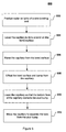
- Figure 5 is a flowchart illustrating the steps used to form stud bumps 106 according to one embodiment of the invention.
- Figure 5 may be viewed in conjunction with Figures 6A-6E , which are simplified cross-sectional drawings of a wire bonding tool at various stages of the stud bump formation process according to an embodiment of the invention.
- a semiconductor wafer such as wafer 300 shown in Fig. 3
- Wafer 300 has formed thereon a plurality of integrated circuits, each of which includes a plurality of bonding pads (represented in Figures 6A-6E as bonding surfaces 612).
- the wire bonding tool includes a capillary 602 with a bottom face 606 that is positioned above bonding surface 612 during the wire bonding operation.
- Wire bonding tool also includes a feed hole (not labeled) for receiving a wire 608 and a chamfer 604 surrounding the feed hole at the bottom face 606.
- Capillary 602 contains a wire 608 that can be gradually extruded from feed hole 614 in capillary 602.
- wire 608 may be housed within a threaded capillary used for precise control over the amount of wire 608 extended from capillary 602.
- An electric flame-off tool (not shown) may be used to form the end of wire 608 into a free air ball (not shown) for optimal deposition.
- the free air ball can then be captured by the capillary 602 within the chamfer area 604 and then lowered to the bond surface 612 to form stud bump 610.
- step 504 capillary 602 is lowered so that the extruded portion of wire 608 is contacts and forms a bond on bond surface 612 (step 504).
- a number of different wire bonding techniques may be utilized to form and bond stud bump 610 to bond surface 612 including compression bonding, thermo-compression bonding, thermosonic bonding and ultrasonic bonding. Through the application of mechanical force, heat, and/or ultrasonic energy, a bond is formed between stud bump 610 and bond surface 612.
- Bond surface 612 may be for example, a bond pad overlying a semiconductor die, which includes one or more active devices.
- the initial formation of stud bump 610 at this stage is shown in Figure 6A .
- Capillary 602 is then raised from bond surface 612 while allowing stud bump 610 to stay in contact with bond surface 612 without breaking wire 608 (step 506). Thus, stud bump 610 is still coupled with wire 608 during process 506. The result of this process is shown in Figure 6B .
- bond surface 612 and stud bump 610 are offset from capillary 602 by an width W (step 508) while the wire is still attached to the top of the stud bump.
- the offset may be accomplished by displacing a table removably coupled with the semiconductor die thus translating bond surface 612 and stud bump 610 in a lateral direction.
- capillary 602 may also be moved while keeping bond surface 612 and stud bump 610 stationary.
- width W is in the range of 1.0-2.0 times the diameter of the wire size.
- Capillary 602 is then lowered downward so that the bottom face 606 of capillary 602 contacts stud bump 610 pressing the pulled portion of the wire (still connected to the top of the stud bump) downwards onto the top surface of the stud bump (step 510).
- This step flattens the top of stud bump 610 and forms what is referred to herein as a second bond.
- the flattened surface on stud bump 610 allows for easier deposition and adhesion of the solder paste onto the stud bump as a result of the increased amount of sidewall surface as compared to a more vertical surface. The result of this process is shown in Figure 6D .
- capillary 602 is moved upwards to separate wire 608 from stud bump 610 (step 512).
- the upwards movement of the entire capillary serves to break wire 608 away from stud bump 610, which remains bonded to bond surface 612. Because of the strong bond created by the previous steps, the pulling up and breaking of the wire does not affect the flattened profile of the top of stud bump 610.
- Figure 6E The result of this process is shown in Figure 6E .
- a clean break between wire 608 and bond surface 612 can be obtained so that the process flow 500 can be repeated to form additional stud bumps on the remaining bond pads. Examples of the height and width of typical stud bumps formed using the processes described in Figures 6A-6E is set forth in Table 1 below.
- Figures 7A-7C are diagrams showing different capillary designs that can be used to form bumps of varying heights according to an embodiments of the present invention.
- the angles and dimensions described shown in Figure 7A may be used by one of skill in the art to design a capillary where ball height is 70% of the eventually desired overall bump height.
- Figures 7B and 7C show angles and dimensions that may be used to design capillaries with different internal chamfer angles to form a desired bump size.
- the use of different angle selection parameters allows for increased flexibility as all that is needed to change the wire-bonding device is a change in the bumping parameters used in the capillary.
- stacked stud bumps can be formed to increase the height of the stud bump for particular packages.
- FIG 8 is a simplified cross-sectional drawing of a wafer-level package incorporating a stacked stud bump design according to an embodiment of the present invention.
- Wafer-level package 800 shown in Figure 8 may be used if an increased height of the stud bumps is required to couple wafer-level package 800 with a printed circuit device or other device.
- Figure 8 shares many similar elements with Figure 1 , such as semiconductor die 102, bond pads 104, passivation layer 112, encapsulation layer 108, and solder 110.
- package 800 includes stacked stud bumps formed by stacking stud bumps 814 directly on top of stud bumps 106.
- Stud bump 814 is essentially formed by repeating the stud bump formation process described in Figs. 5 and 6A-6E a second time.
- Stud bump 806 is formed directly overlying first stud bump 106 and provides additional height to the package 800 for improved interconnections.
- stacked stud bumps comprising two, three, or more stud bumps are possible, depending upon the specific bump height requirements of the package.
- a typical height of the stacked stud bump 106, 806 is between 3-6 mm, about twice the height of the stud bumps formed in package 100.
- a stacked bump design allows for an increased bump height without increasing the bump diameter, as often required by area-array packages.
- the same material e.g., copper
- the same material is used to form the all of the multiple stud bumps in a stacked stud bump configuration.
- An alternate method of increasing the bump height is to use wire of a greater diameter, as the eventual bump height following formation is correlated with the diameter of the wire used.
- the bump height obtained may be comparable to that obtained using a stacked bump process.
- copper wire with a diameter between 1-4 mm can be used to form the stud bumps.
- stud bumps 104 have been described as being formed using a copper process, other suitable wire materials that can be used for ball bonding can be used instead of copper to form the stud bumps.
- the stud bumps can be made out of gold or aluminum wires in other embodiments.
Abstract
Description
- The present invention relates to generally to integrated circuit packaging technology. More specifically, embodiments of the invention pertain to the use of wire bonding techniques to form stud bumps for wafer-level packages.
- Integrated circuits are typically packaged before being used in electronic systems. Integrated circuit (IC) packages protect the integrated circuits from the surrounding environment and provide electrical connections to other components of the electronic systems. In a conventional packaging arrangement, a wafer containing integrated circuits is first singulated into individual chips and then packaged for testing and delivery. This normally includes transporting the wafer (or singulated chips) from a semiconductor manufacturing facility where front-end processes are performed to a separate packaging facility where back-end process are performed to assemble and package the IC.
- In contrast, in a wafer-level packaging approach. IC packaging is formed at the wafer level on the wafer prior to singulation. The packages can be manufactured at chip size and at reduced cost compared to standard IC packages. Typical wafer level packages use solder bumps to form electrical connections between the packaged semiconductor die and external devices. Under bump metallurgy (UMB) is formed underneath the solder bumps to minimize metallurgical reactions with the solder and improve the connection.
- While a number of commercially successful wafer-level packaging processes have been developed, improved waver level packages are desirable.
- The present invention relates to generally to wafer level packaging technology. More specifically, embodiments of the invention pertain to the use of wire bonding techniques to form stud bumps for wafer-level packages,
- In one embodiment of the present invention, a method of fabricating a wafer level package is described. The method includes fabricating at least one active device on a semiconductor wafer that has not been singulated where the active device having a plurality of bonding pads exposed at an upper surface of the wafer. Prior to singulating the semiconductor wafer, a plurality of corresponding stud bumps are formed on the plurality of bonding pads with a wire bonding tool. Thereafter, a molding encapsulation layer is applied over the semiconductor wafer leaving an upper portion of each of the plurality of stud bumps exposed.
- In some embodiments, the stud bumps are formed by lowering the capillary of the wire bonding tool towards the semiconductor wafer to allow an extruded portion of the wire from the feed hole to contact and form a first bond with a corresponding bond pad without breaking the wire; raising the capillary away from the semiconductor wafer while allowing the extruded portion of the wire to stay in contact with the bond pad without breaking the wire; offsetting the capillary from the first bond in a direction parallel to the upper surface of the semiconductor wafer; lowering the capillary so that the bottom face of the capillary contacts the stud bump and flattens a top surface of the stud bump; and moving the capillary away from the semiconductor die to separate the wire from the stud bump.
- In another embodiment of the present invention, a method of fabricating a plurality of wafer-level packages is described. The method includes fabricating a plurality of active devices on a semiconductor wafer that has not been singulated. Each of the active devices has a plurality of bonding pads exposed at an upper surface of the wafer. Prior to singulating the semiconductor wafer to separate the plurality of active devices, for each of the plurality of active devices the method includes: forming a plurality of stud bumps corresponding to the plurality of bonding pads associated with the active device using a wire bonding tool; applying a molding encapsulation layer over the semiconductor wafer leaving an upper portion of each of the plurality of stud bumps formed on each of the active devices exposed; applying solder paste over each of the exposed of stud bumps; reflowing the solder paste; and cleaning the substrate with flux. In some specific embodiments the plurality of stud bumps are copper stud bumps.
- In yet another specific embodiment of the present invention a semiconductor wafer package is provided. The package includes a semiconductor die having an upper surface, a plurality of bonding pads formed on the semiconductor die, and a plurality of stud bumps corresponding to the plurality of bonding pads. Each stud bump is directly coupled to a bonding pad without under bump metallization between the stud bump and the bonding pad. The package additionally includes an encapsulation layer overlying the semiconductor die which leaves an upper portion of each of the plurality of stud bumps exposed. In some specific embodiments the plurality of stud bumps are copper stud bumps.
- These and other embodiments of the present invention, as well its advantages and features, are described in more detail in conjunction with the description below and attached figures.
-
Figure 1 is a simplified cross-sectional drawing of a wafer-level package incorporating stud bumps according to one embodiment of the invention; -
Figure 2 is a flowchart illustrating steps employed in the formation and singulation of a wafer-level package according to an embodiment of the present invention; -
Figure 3 is a simplified process flow showing the formation and singulation of a wafer-level package according to the steps recited in the flowchart ofFig. 2 ; -
Figures 4A-4D are simplified cross-sectional drawings of a wafer level package at various stages of formation as set forth infigs. 2 and3 ; -
Figure 5 is a flowchart illustrating steps employed in a stud bumping process according to one embodiment of the invention; -
Figures 6A-6E are simplified cross-sectional drawings of the formation of a wafer-level package incorporating stud bumps according to an embodiment of the present invention; -
Figures 7A-7C are diagrams showing the selection of angles used to form bumps of varying heights according to embodiments of the present invention; -
Figure 8 is a simplified cross-sectional drawing of a wafer-level package incorporating stacked stud bumps according to another embodiment of the invention. - The present invention relates to generally to wafer level packaging technology. More specifically, embodiments of the invention pertain to the use of wire bonding techniques used to form stud bumps for wafer-level packages.
-
Figure 1 is a simplified cross-sectional drawing of a wafer-level package 100 according to an embodiment of the present invention.Package 100 includes a semiconductor die 102 having one or more active devices (not shown) formed thereon using conventional semiconductor manufacturing processes during front-end processing. The active devices includebond pads 104 which may be made from aluminum or other suitable materials and apassivation layer 112. Passivation layer electrically isolatesbond pads 104 from each other to prevent short-circuiting of the active devices and may be, for example, a nitride layer or other suitable material.Bond pads 104 can be designed and fabricated in a peripheral format, array format or any other suitable arrangement. - Wafer-
level package 100 further includesstud bumps 106 coated withsolder 110 as interconnects for the package.Stud bumps 106 are formed using wire bonding techniques as described in detail below directly overbond pads 104 without an intermediate under-bump metallization layer used in conventional wafer level packages. In one embodiment,stud bumps 106 are made from copper wire but other embodiments of the invention can use wire made from other suitable materials to form the stud bumps. - A
mold encapsulation layer 108 surrounds the outside surface ofstud bumps 106 providing stability and environmental protection to wafer-level package 100.Mold encapsulation layer 108 may be formed from plastic or epoxy and does not cover the entirety ofstud bumps 106. The protrusion ofstud bumps 106 frommold encapsulation layer 108 allows electrical connection between the active devices within semiconductor die 102 and an exterior portion of the package. -
Figure 2 is a flow chart illustrating steps used in the formation and singulation of a wafer-level package according to an embodiment of the present invention. To better understand the invention,Figure 2 may be viewed in conjunction withFigure 3 , a simplified process flow showing the formation and singulation of a wafer-level package according to an embodiment of the present invention. - Referring to
Figs. 2 and3 , awafer 300 is provided (Step 202). Wafer 300 includes a semiconductor die 302 having active devices formed thereon and bond pads overlying the semiconductor die. Stud bumps are then formed overlying the bond pads (Step 204). The result of this process is shown as partially completed package in 304. A molding encapsulation process is then performed (Step 206) that leaves an upper portion of the stud bumps exposed in a partially completed package in 306. - In a specific embodiment of the present invention, the molding encapsulates 1/2-3/4 of the total bump height of the stud bumps. In another embodiment, the molding layer completely encapsulates the stud bumps when initially deposited but is then opened to expose the stud bumps using a laser, back grinding or other technique. The protrusion of stud bumps 106 (
Fig. 1 ) frommold encapsulation layer 108 provides for leads between the active devices within semiconductor die 102 and an exterior portion of the package. In addition, the use ofmold encapsulation layer 108 obviates the need for an underfill layer, thus reducing the number of processes needed to fully package the devices for shipment. In another embodiment of the present invention, over molding can be used to completely encapsulatepackage 100, with an etching, laser etching, or grinding process then used to expose the stud bumps. - A screen printing or solder dipping process is then used to deposit a layer of solder paste on top of the stud bumps (Step 208) forming partially completed
package 308, and a reflow process (Step 210) is used to form the solder into ball interconnects better suited for electrical interconnection as shown in partially completed package in 310. In one embodiment, tin may be used as the solder material but other appropriate solders may be used as well. - The wafer is then cleaned using a flux cleaning process as known to those of skill in the art to remove oxidation from the solder overlying the stud bumps (Step 212). In addition to removal of potential oxidation from the solder, the flux cleaning process also serves to improve wetting characteristics of the solder for improved bonds between the balls and a printed circuit board or other device. The result of this process is shown as partially completed
package 312. - The wafer is then singulated into individual packaged IC integrated circuits 314 (Step 214), which can be packaged onto tape and reel or waffle packs for shipment as a finished product to customers. Each wafer-
level package 314 formed after singulation includes one or more active devices. In some embodiments wafer-level test and burn-in of the chips is performed prior to singulation. This offers cost-savings as compared to individually performing similar processes upon each chip package after singulation. -
Figs. 4A-4D represent simplified cross-sectional views of a wafer-level package 100 at the various steps of formation described inFigs. 2 and3 . Specifically,Fig. 4A showspackage 100 atstep 202 ofFig. 2 ;Fig. 4B showspackage 100 atstep 204;Fig. 4C shows the package atstep 206 andFig. 4D shows the package atstep 208. - A wafer-level package formed according to the steps set forth in
Figure 2 can be formed at a lower cost than conventional implementations. The use of wire-bonding to form the stud bump obviates the need to use an under-bump metallization layer, while still maintaining a reliable interconnection between the stud bump and the underlying bond pad. This, in turn, reduces the need for masking, etching, or plating processes that are normally used to form the under-bump metallization layer. In addition, the completedwafer package 100 has sufficient structural strength that it meets the standard board-level reliability metrics for wafer-level packaging without employing an underfill layer for board mounting in some embodiments of the invention. -
Figure 5 is a flowchart illustrating the steps used to form stud bumps 106 according to one embodiment of the invention.Figure 5 may be viewed in conjunction withFigures 6A-6E , which are simplified cross-sectional drawings of a wire bonding tool at various stages of the stud bump formation process according to an embodiment of the invention. - As shown in
Figure 5 , a semiconductor wafer, such aswafer 300 shown inFig. 3 , is positioned on a table associated with an appropriate wire bonding tool (step 502).Wafer 300 has formed thereon a plurality of integrated circuits, each of which includes a plurality of bonding pads (represented inFigures 6A-6E as bonding surfaces 612). The wire bonding tool includes a capillary 602 with abottom face 606 that is positioned abovebonding surface 612 during the wire bonding operation. Wire bonding tool also includes a feed hole (not labeled) for receiving awire 608 and achamfer 604 surrounding the feed hole at thebottom face 606. -
Capillary 602 contains awire 608 that can be gradually extruded from feed hole 614 incapillary 602. For example,wire 608 may be housed within a threaded capillary used for precise control over the amount ofwire 608 extended fromcapillary 602. An electric flame-off tool (not shown) may be used to form the end ofwire 608 into a free air ball (not shown) for optimal deposition. The free air ball can then be captured by the capillary 602 within thechamfer area 604 and then lowered to thebond surface 612 to formstud bump 610. - During the bond
formation process capillary 602 is lowered so that the extruded portion ofwire 608 is contacts and forms a bond on bond surface 612 (step 504). A number of different wire bonding techniques may be utilized to form andbond stud bump 610 tobond surface 612 including compression bonding, thermo-compression bonding, thermosonic bonding and ultrasonic bonding. Through the application of mechanical force, heat, and/or ultrasonic energy, a bond is formed betweenstud bump 610 andbond surface 612.Bond surface 612 may be for example, a bond pad overlying a semiconductor die, which includes one or more active devices. The initial formation ofstud bump 610 at this stage is shown inFigure 6A . -
Capillary 602 is then raised frombond surface 612 while allowingstud bump 610 to stay in contact withbond surface 612 without breaking wire 608 (step 506). Thus,stud bump 610 is still coupled withwire 608 duringprocess 506. The result of this process is shown inFigure 6B . Next,bond surface 612 andstud bump 610 are offset fromcapillary 602 by an width W (step 508) while the wire is still attached to the top of the stud bump. The offset may be accomplished by displacing a table removably coupled with the semiconductor die thus translatingbond surface 612 andstud bump 610 in a lateral direction. Alternatively, capillary 602 may also be moved while keepingbond surface 612 andstud bump 610 stationary. The effect of the lateral offset is thatcapillary 602 is shifted a width W from thebond surface 612 andstud bump 610. In some embodiments, width W is in the range of 1.0-2.0 times the diameter of the wire size. The result of this process is shown inFigure 6C . -
Capillary 602 is then lowered downward so that thebottom face 606 of capillary 602contacts stud bump 610 pressing the pulled portion of the wire (still connected to the top of the stud bump) downwards onto the top surface of the stud bump (step 510). This step flattens the top ofstud bump 610 and forms what is referred to herein as a second bond. The flattened surface onstud bump 610 allows for easier deposition and adhesion of the solder paste onto the stud bump as a result of the increased amount of sidewall surface as compared to a more vertical surface. The result of this process is shown inFigure 6D . - Next,
capillary 602 is moved upwards toseparate wire 608 from stud bump 610 (step 512). The upwards movement of the entire capillary serves to breakwire 608 away fromstud bump 610, which remains bonded tobond surface 612. Because of the strong bond created by the previous steps, the pulling up and breaking of the wire does not affect the flattened profile of the top ofstud bump 610. The result of this process is shown inFigure 6E . By utilizing this process, a clean break betweenwire 608 andbond surface 612 can be obtained so that theprocess flow 500 can be repeated to form additional stud bumps on the remaining bond pads. Examples of the height and width of typical stud bumps formed using the processes described inFigures 6A-6E is set forth in Table 1 below.Table 1 Wire Size Bump Type Bump Height Bump Size 1.0 mil Single bump 50 ± 10 µm 85 ± 10 µm 1.0 mil Two stack bump 90 ± 10 µm 90 ± 10 µm 1.0 mil Three stack bump 125 ± 10 µm 95 ± 10 µm 2.0 mil Single bump 101 ± 10 µm 140 ± 10 µm 4.0 mil Single bump 150 ± 10 µm 317 ± 20 µm -
Figures 7A-7C are diagrams showing different capillary designs that can be used to form bumps of varying heights according to an embodiments of the present invention. For example, the angles and dimensions described shown inFigure 7A may be used by one of skill in the art to design a capillary where ball height is 70% of the eventually desired overall bump height. Similarly,Figures 7B and 7C show angles and dimensions that may be used to design capillaries with different internal chamfer angles to form a desired bump size. The use of different angle selection parameters allows for increased flexibility as all that is needed to change the wire-bonding device is a change in the bumping parameters used in the capillary. - In some embodiments of the invention, stacked stud bumps can be formed to increase the height of the stud bump for particular packages. An example of such a package is illustrated in
Figure 8 , which is a simplified cross-sectional drawing of a wafer-level package incorporating a stacked stud bump design according to an embodiment of the present invention. Wafer-level package 800 shown inFigure 8 may be used if an increased height of the stud bumps is required to couple wafer-level package 800 with a printed circuit device or other device.Figure 8 shares many similar elements withFigure 1 , such as semiconductor die 102,bond pads 104,passivation layer 112,encapsulation layer 108, andsolder 110. The primary difference betweenpackage 100 andpackage 800 is thatpackage 800 includes stacked stud bumps formed by stacking stud bumps 814 directly on top of stud bumps 106. Stud bump 814 is essentially formed by repeating the stud bump formation process described inFigs. 5 and6A-6E a second time.Stud bump 806 is formed directly overlyingfirst stud bump 106 and provides additional height to thepackage 800 for improved interconnections. Thus, stacked stud bumps comprising two, three, or more stud bumps are possible, depending upon the specific bump height requirements of the package. For example, a typical height of the stackedstud bump package 100. The use of a stacked bump design allows for an increased bump height without increasing the bump diameter, as often required by area-array packages. Typically, the same material (e.g., copper) is used to form the all of the multiple stud bumps in a stacked stud bump configuration. - An alternate method of increasing the bump height is to use wire of a greater diameter, as the eventual bump height following formation is correlated with the diameter of the wire used. By using thicker wire and appropriate parameters, the bump height obtained may be comparable to that obtained using a stacked bump process. For example, copper wire with a diameter between 1-4 mm can be used to form the stud bumps.
- The description above has been given to help illustrate the principles of this invention. It is not intended to limit the scope of this invention in any way. A large variety of variants are apparent, which are encompassed within the scope of this invention.
- While the stud bumps 104 have been described as being formed using a copper process, other suitable wire materials that can be used for ball bonding can be used instead of copper to form the stud bumps. As an example, the stud bumps can be made out of gold or aluminum wires in other embodiments. Also, while the invention has been described in detail and with reference to specific examples thereof, it will be apparent to one skilled in the art that various changes and modifications can be made therein without departing from the spirit and scope thereof.
Claims (16)
- A method of fabricating a wafer-level package comprising:fabricating at least one active device on a semiconductor wafer that has not been singulated, the active device having a plurality of bonding pads exposed at an upper surface of the wafer; andprior to singulating the semiconductor wafer: (i) forming a plurality of corresponding stud bumps on the plurality of bonding pads, and thereafter (ii) applying a molding encapsulation layer over the semiconductor wafer leaving an upper portion of each of the plurality of stud bumps exposed.
- A method as set forth in claim 1 wherein the height of the stud bumps is increased by forming stacked stud bumps or increasing a diameter of a wire from which the stud bumps are formed.
- A method as set forth in claim 1 or 2 wherein the molding encapsulation layer completely encapsulates the stud bumps when initially applied and the stud bumps are exposed with a laser, back grinding or other process.
- A method as set forth in any one of the preceding claims further comprising coating each of the plurality of stud bumps with solder, and optionally:reflowing the solder;using a flux cleaning process to clean the stud bumps; andthereafter, singulating the semiconductor wafer to form a plurality of wafer-level packages.
- A method of fabricating a wafer-level package set forth in any one of the preceding claims wherein the plurality of bonding pads are in peripheral format or array format.
- The method of fabricating a wafer-level package set forth in any one of the preceding claims wherein the wire bonding tool used to form the plurality of stud bumps includes a capillary having a feed hole for dispensing a wire, a bottom face, and a chamfer surrounding the feed hole at the bottom face, and wherein each of the plurality of stud bumps formed on the bonding pads is formed by:lowering the capillary towards the semiconductor wafer to allow an extruded portion of the wire from the feed hole to contact and form a first bond with a corresponding bond pad without breaking the wire;raising the capillary away from the semiconductor wafer while allowing the extruded portion of the wire to stay in contact with the bond pad without breaking the wire;offsetting the capillary from the first bond in the direction parallel to the upper surface of the semiconductor wafer;lowering the capillary so that the bottom face of the capillary contacts the stud bump and flattens a top surface of the stud bump; andmoving the capillary away from the semiconductor die to separate the wire from the stud bump.
- A method of fabricating a plurality of wafer-level packages comprising:fabricating a plurality of active devices on a semiconductor wafer that has not been singulated, wherein each of the active devices has a plurality of bonding pads exposed at an upper surface of the wafer; andprior to singulating the semiconductor wafer to separate the plurality of active devices: (i) for each of the plurality of active devices, forming a plurality of copper stud bumps corresponding to the plurality of bonding pads associated with the active device using a wire bonding tool, (ii) applying a molding encapsulation layer over the semiconductor wafer leaving an upper portion of each of the plurality of stud bumps formed on each of the active devices exposed, (iii) applying solder paste over each of the exposed of copper stud bumps, (iv) reflowing the solder paste, and (v) cleaning the substrate with flux.
- A method as set forth in claim 7 further comprising singulating the semiconductor wafer to separate the plurality of active devices and form the plurality of wafer-level packages, for example so that each wafer-level package comprises a single active device.
- The method as set forth in any one of the preceding claims wherein the plurality of stud bumps are stacked stud bumps, where each stacked stud bump is formed by forming a plurality of stud bumps directly overlying each other, wherein each of the plurality of stud bumps in a stack of stud bumps is formed with a wire bonding tool.
- The method set forth in any one of the preceding claims wherein the plurality of stud bumps formed on the plurality of bonding pads are copper, gold or aluminium stud bumps.
- The method as set forth in any one of the preceding claims wherein the molding encapsulation layer encapsulates between 50-75% of the bump height of the stud bumps.
- A semiconductor wafer package comprising:a semiconductor die having an upper surface;a plurality of bonding pads formed on the semiconductor die;a plurality of copper stud bumps corresponding to the plurality of bonding pads, each copper stud bumps being directly coupled to a bonding pad without under bump metallization between the stud bump and the bonding pad; andan encapsulation layer overlying the semiconductor die while leaving an upper portion of each of the plurality of stud bumps exposed.
- The semiconductor wafer package set forth in claim 14 further comprising a plurality of solder balls corresponding to the plurality of copper stud bumps, wherein each solder ball is attached to a respective one of the copper stud bumps.
- The semiconductor wafer package set forth in claim 12 or 13 wherein each of the plurality of the stud bumps is a stacked stud bump comprising a plurality of copper bumps stacked on top of each other and/or the package does not include underfill and has sufficient structural strength to meet standard board-level reliability metrics for a wafer-level package.
- A method of forming a stud bump on a semiconductor die using a wire bonding tool including a capillary having a feed hole for dispensing a wire, a bottom face and a chamfer surrounding the feed hole at the bottom face, the method comprising:providing a semiconductor wafer upon which the semiconductor die is formed;prior to singulating the semiconductor wafer:(a) lowering the capillary towards the semiconductor wafer to allow an extruded portion of the wire from the feed hole to contact and form a first bond with a corresponding bond pad without breaking the wire;(b) raising the capillary away from the semiconductor wafer while allowing the extruded portion of the wire to stay in contact with the bond pad without breaking the wire;(c) offsetting the capillary from the first bond in a direction parallel to the upper surface of the semiconductor wafer;(d) lowering the capillary so that the bottom face of the capillary contacts the stud bump and flattens a top surface of the stud bump; and(e) moving the capillary away from the semiconductor die to separate the wire from the stud bump.
- The method of forming a stud bump as recited in claim 15 wherein the step of lowering the capillary towards the semiconductor die further comprises applying mechanical force, heat, or ultrasonic energy to improve the bond between the extruded portion of the wire and the bond pad; wherein the step of offsetting the capillary comprises displacing a table upon which the semiconductor wafer is positioned during the wire bonding process; and wherein the step of lowering the capillary to flatten a top surface of the stud bump further comprises allowing an extended portion of the wire to form a second bond adjacent to the first bond where the stud bump is made up of the first and second bonds.
Applications Claiming Priority (1)
| Application Number | Priority Date | Filing Date | Title |
|---|---|---|---|
| MYPI20084228 MY149251A (en) | 2008-10-23 | 2008-10-23 | Wafer-level package using stud bump coated with solder |
Publications (2)
| Publication Number | Publication Date |
|---|---|
| EP2180505A2 true EP2180505A2 (en) | 2010-04-28 |
| EP2180505A3 EP2180505A3 (en) | 2013-02-27 |
Family
ID=41479103
Family Applications (1)
| Application Number | Title | Priority Date | Filing Date |
|---|---|---|---|
| EP20090252154 Withdrawn EP2180505A3 (en) | 2008-10-23 | 2009-09-10 | Wafer-level fabrication of a package with stud bumps coated with solder |
Country Status (4)
| Country | Link |
|---|---|
| US (2) | US8071470B2 (en) |
| EP (1) | EP2180505A3 (en) |
| CN (1) | CN101728287A (en) |
| MY (1) | MY149251A (en) |
Cited By (3)
| Publication number | Priority date | Publication date | Assignee | Title |
|---|---|---|---|---|
| WO2013055453A3 (en) * | 2011-10-10 | 2013-06-13 | Conexant Systems, Inc. | Solder-coated copper stud bump wafer level package and manufacturing method thereof |
| US10598874B2 (en) | 2017-11-02 | 2020-03-24 | International Business Machines Corporation | Fabrication method of high aspect ratio solder bumping with stud bump and injection molded solder, and flip chip joining with the solder bump |
| FR3088018A1 (en) * | 2018-11-06 | 2020-05-08 | Mbda France | BREWING LINKAGE METHOD FOR IMPROVING FATIGUE HOLDING OF BRAZED JOINTS |
Families Citing this family (82)
| Publication number | Priority date | Publication date | Assignee | Title |
|---|---|---|---|---|
| JP5592055B2 (en) | 2004-11-03 | 2014-09-17 | テッセラ,インコーポレイテッド | Improved stacking packaging |
| US8058101B2 (en) | 2005-12-23 | 2011-11-15 | Tessera, Inc. | Microelectronic packages and methods therefor |
| US7608484B2 (en) * | 2006-10-31 | 2009-10-27 | Texas Instruments Incorporated | Non-pull back pad package with an additional solder standoff |
| US8482111B2 (en) | 2010-07-19 | 2013-07-09 | Tessera, Inc. | Stackable molded microelectronic packages |
| US9159708B2 (en) | 2010-07-19 | 2015-10-13 | Tessera, Inc. | Stackable molded microelectronic packages with area array unit connectors |
| KR101075241B1 (en) | 2010-11-15 | 2011-11-01 | 테세라, 인코포레이티드 | Microelectronic package with terminals on dielectric mass |
| US20120146206A1 (en) | 2010-12-13 | 2012-06-14 | Tessera Research Llc | Pin attachment |
| KR101128063B1 (en) | 2011-05-03 | 2012-04-23 | 테세라, 인코포레이티드 | Package-on-package assembly with wire bonds to encapsulation surface |
| US8618659B2 (en) | 2011-05-03 | 2013-12-31 | Tessera, Inc. | Package-on-package assembly with wire bonds to encapsulation surface |
| US8829676B2 (en) * | 2011-06-28 | 2014-09-09 | Taiwan Semiconductor Manufacturing Company, Ltd. | Interconnect structure for wafer level package |
| CN103797569A (en) * | 2011-07-06 | 2014-05-14 | 弗莱克斯电子有限责任公司 | Solder desposition system and method for metal bumps |
| US8404520B1 (en) | 2011-10-17 | 2013-03-26 | Invensas Corporation | Package-on-package assembly with wire bond vias |
| US9691706B2 (en) * | 2012-01-23 | 2017-06-27 | Taiwan Semiconductor Manufacturing Company, Ltd. | Multi-chip fan out package and methods of forming the same |
| US8643150B1 (en) * | 2012-02-15 | 2014-02-04 | Maxim Integrated Products, Inc. | Wafer-level package device having solder bump assemblies that include an inner pillar structure |
| US9583425B2 (en) * | 2012-02-15 | 2017-02-28 | Maxim Integrated Products, Inc. | Solder fatigue arrest for wafer level package |
| US8946757B2 (en) | 2012-02-17 | 2015-02-03 | Invensas Corporation | Heat spreading substrate with embedded interconnects |
| US8372741B1 (en) | 2012-02-24 | 2013-02-12 | Invensas Corporation | Method for package-on-package assembly with wire bonds to encapsulation surface |
| US9349706B2 (en) | 2012-02-24 | 2016-05-24 | Invensas Corporation | Method for package-on-package assembly with wire bonds to encapsulation surface |
| US9263412B2 (en) | 2012-03-09 | 2016-02-16 | Taiwan Semiconductor Manufacturing Company, Ltd. | Packaging methods and packaged semiconductor devices |
| US20130234317A1 (en) * | 2012-03-09 | 2013-09-12 | Taiwan Semiconductor Manufacturing Company, Ltd. | Packaging Methods and Packaged Semiconductor Devices |
| US8531040B1 (en) | 2012-03-14 | 2013-09-10 | Honeywell International Inc. | Controlled area solder bonding for dies |
| US9515036B2 (en) * | 2012-04-20 | 2016-12-06 | Taiwan Semiconductor Manufacturing Company, Ltd. | Methods and apparatus for solder connections |
| US8835228B2 (en) | 2012-05-22 | 2014-09-16 | Invensas Corporation | Substrate-less stackable package with wire-bond interconnect |
| US9391008B2 (en) | 2012-07-31 | 2016-07-12 | Invensas Corporation | Reconstituted wafer-level package DRAM |
| US9502390B2 (en) | 2012-08-03 | 2016-11-22 | Invensas Corporation | BVA interposer |
| US9627347B2 (en) * | 2012-09-24 | 2017-04-18 | National Institute Of Advanced Industrial Science And Technology | Method of manufacturing semiconductor device and semiconductor device manufacturing apparatus |
| US8975738B2 (en) | 2012-11-12 | 2015-03-10 | Invensas Corporation | Structure for microelectronic packaging with terminals on dielectric mass |
| US9704780B2 (en) | 2012-12-11 | 2017-07-11 | STATS ChipPAC, Pte. Ltd. | Semiconductor device and method of forming low profile fan-out package with vertical interconnection units |
| US9240331B2 (en) | 2012-12-20 | 2016-01-19 | Stats Chippac, Ltd. | Semiconductor device and method of making bumpless flipchip interconnect structures |
| US9287204B2 (en) | 2012-12-20 | 2016-03-15 | Stats Chippac, Ltd. | Semiconductor device and method of bonding semiconductor die to substrate in reconstituted wafer form |
| US9245770B2 (en) | 2012-12-20 | 2016-01-26 | Stats Chippac, Ltd. | Semiconductor device and method of simultaneous molding and thermalcompression bonding |
| US8878353B2 (en) | 2012-12-20 | 2014-11-04 | Invensas Corporation | Structure for microelectronic packaging with bond elements to encapsulation surface |
| US9136254B2 (en) | 2013-02-01 | 2015-09-15 | Invensas Corporation | Microelectronic package having wire bond vias and stiffening layer |
| US9351436B2 (en) * | 2013-03-08 | 2016-05-24 | Cochlear Limited | Stud bump bonding in implantable medical devices |
| US9368460B2 (en) | 2013-03-15 | 2016-06-14 | Taiwan Semiconductor Manufacturing Company, Ltd. | Fan-out interconnect structure and method for forming same |
| US8883563B1 (en) | 2013-07-15 | 2014-11-11 | Invensas Corporation | Fabrication of microelectronic assemblies having stack terminals coupled by connectors extending through encapsulation |
| US9023691B2 (en) | 2013-07-15 | 2015-05-05 | Invensas Corporation | Microelectronic assemblies with stack terminals coupled by connectors extending through encapsulation |
| US9034696B2 (en) | 2013-07-15 | 2015-05-19 | Invensas Corporation | Microelectronic assemblies having reinforcing collars on connectors extending through encapsulation |
| US9167710B2 (en) | 2013-08-07 | 2015-10-20 | Invensas Corporation | Embedded packaging with preformed vias |
| US9685365B2 (en) | 2013-08-08 | 2017-06-20 | Invensas Corporation | Method of forming a wire bond having a free end |
| US20150076714A1 (en) | 2013-09-16 | 2015-03-19 | Invensas Corporation | Microelectronic element with bond elements to encapsulation surface |
| US9508702B2 (en) * | 2013-09-27 | 2016-11-29 | Freescale Semiconductor, Inc. | 3D device packaging using through-substrate posts |
| US9515006B2 (en) * | 2013-09-27 | 2016-12-06 | Freescale Semiconductor, Inc. | 3D device packaging using through-substrate posts |
| US9508701B2 (en) | 2013-09-27 | 2016-11-29 | Freescale Semiconductor, Inc. | 3D device packaging using through-substrate pillars |
| US9087815B2 (en) | 2013-11-12 | 2015-07-21 | Invensas Corporation | Off substrate kinking of bond wire |
| US9082753B2 (en) | 2013-11-12 | 2015-07-14 | Invensas Corporation | Severing bond wire by kinking and twisting |
| US9263394B2 (en) | 2013-11-22 | 2016-02-16 | Invensas Corporation | Multiple bond via arrays of different wire heights on a same substrate |
| US9379074B2 (en) | 2013-11-22 | 2016-06-28 | Invensas Corporation | Die stacks with one or more bond via arrays of wire bond wires and with one or more arrays of bump interconnects |
| US9583456B2 (en) | 2013-11-22 | 2017-02-28 | Invensas Corporation | Multiple bond via arrays of different wire heights on a same substrate |
| US9583411B2 (en) | 2014-01-17 | 2017-02-28 | Invensas Corporation | Fine pitch BVA using reconstituted wafer with area array accessible for testing |
| US9355997B2 (en) | 2014-03-12 | 2016-05-31 | Invensas Corporation | Integrated circuit assemblies with reinforcement frames, and methods of manufacture |
| US20150262902A1 (en) | 2014-03-12 | 2015-09-17 | Invensas Corporation | Integrated circuits protected by substrates with cavities, and methods of manufacture |
| US9214454B2 (en) | 2014-03-31 | 2015-12-15 | Invensas Corporation | Batch process fabrication of package-on-package microelectronic assemblies |
| US9165793B1 (en) | 2014-05-02 | 2015-10-20 | Invensas Corporation | Making electrical components in handle wafers of integrated circuit packages |
| US10381326B2 (en) | 2014-05-28 | 2019-08-13 | Invensas Corporation | Structure and method for integrated circuits packaging with increased density |
| US9646917B2 (en) | 2014-05-29 | 2017-05-09 | Invensas Corporation | Low CTE component with wire bond interconnects |
| US9412714B2 (en) | 2014-05-30 | 2016-08-09 | Invensas Corporation | Wire bond support structure and microelectronic package including wire bonds therefrom |
| US9741649B2 (en) | 2014-06-04 | 2017-08-22 | Invensas Corporation | Integrated interposer solutions for 2D and 3D IC packaging |
| US9412806B2 (en) | 2014-06-13 | 2016-08-09 | Invensas Corporation | Making multilayer 3D capacitors using arrays of upstanding rods or ridges |
| US9252127B1 (en) | 2014-07-10 | 2016-02-02 | Invensas Corporation | Microelectronic assemblies with integrated circuits and interposers with cavities, and methods of manufacture |
| CN204221161U (en) * | 2014-07-15 | 2015-03-25 | 派克泰克封装技术有限公司 | Soldered ball feed arrangement and induction system |
| US9496154B2 (en) | 2014-09-16 | 2016-11-15 | Invensas Corporation | Use of underfill tape in microelectronic components, and microelectronic components with cavities coupled to through-substrate vias |
| US9735084B2 (en) | 2014-12-11 | 2017-08-15 | Invensas Corporation | Bond via array for thermal conductivity |
| US9806066B2 (en) | 2015-01-23 | 2017-10-31 | Samsung Electronics Co., Ltd. | Semiconductor package including exposed connecting stubs |
| US9888579B2 (en) | 2015-03-05 | 2018-02-06 | Invensas Corporation | Pressing of wire bond wire tips to provide bent-over tips |
| US9502372B1 (en) | 2015-04-30 | 2016-11-22 | Invensas Corporation | Wafer-level packaging using wire bond wires in place of a redistribution layer |
| US9761554B2 (en) | 2015-05-07 | 2017-09-12 | Invensas Corporation | Ball bonding metal wire bond wires to metal pads |
| US9478504B1 (en) | 2015-06-19 | 2016-10-25 | Invensas Corporation | Microelectronic assemblies with cavities, and methods of fabrication |
| FR3041625B1 (en) * | 2015-09-29 | 2021-07-30 | Tronics Microsystems | DEVICE FOR FIXING TWO ELEMENTS SUCH AS A CHIP, AN INTERPOSER AND A BRACKET |
| US9490222B1 (en) | 2015-10-12 | 2016-11-08 | Invensas Corporation | Wire bond wires for interference shielding |
| US10490528B2 (en) | 2015-10-12 | 2019-11-26 | Invensas Corporation | Embedded wire bond wires |
| US10332854B2 (en) | 2015-10-23 | 2019-06-25 | Invensas Corporation | Anchoring structure of fine pitch bva |
| US10181457B2 (en) | 2015-10-26 | 2019-01-15 | Invensas Corporation | Microelectronic package for wafer-level chip scale packaging with fan-out |
| US10043779B2 (en) | 2015-11-17 | 2018-08-07 | Invensas Corporation | Packaged microelectronic device for a package-on-package device |
| US9659848B1 (en) | 2015-11-18 | 2017-05-23 | Invensas Corporation | Stiffened wires for offset BVA |
| US9984992B2 (en) | 2015-12-30 | 2018-05-29 | Invensas Corporation | Embedded wire bond wires for vertical integration with separate surface mount and wire bond mounting surfaces |
| DE102016112390B4 (en) | 2016-07-06 | 2021-08-12 | Infineon Technologies Ag | Solder pad and method for improving the solder pad surface |
| US9935075B2 (en) | 2016-07-29 | 2018-04-03 | Invensas Corporation | Wire bonding method and apparatus for electromagnetic interference shielding |
| US10299368B2 (en) | 2016-12-21 | 2019-05-21 | Invensas Corporation | Surface integrated waveguides and circuit structures therefor |
| US10600756B1 (en) * | 2017-02-15 | 2020-03-24 | United States Of America, As Represented By The Secretary Of The Navy | Wire bonding technique for integrated circuit board connections |
| KR20220029232A (en) | 2020-09-01 | 2022-03-08 | 삼성전자주식회사 | Semiconductor package and semiconductor apparatus comprising the same |
| KR20220056309A (en) | 2020-10-27 | 2022-05-06 | 삼성전자주식회사 | Semiconductor package |
Citations (5)
| Publication number | Priority date | Publication date | Assignee | Title |
|---|---|---|---|---|
| US5908317A (en) * | 1996-03-11 | 1999-06-01 | Anam Semiconductor Inc. | Method of forming chip bumps of bump chip scale semiconductor package |
| JP2000200800A (en) * | 1999-01-06 | 2000-07-18 | Fujitsu Ltd | Semiconductor device and its manufacture |
| US20020056741A1 (en) * | 2000-11-16 | 2002-05-16 | Shieh Wen Lo | Application of wire bonding technology on wafer bump, wafer level chip scale package structure and the method of manufacturing the same |
| US20040018713A1 (en) * | 2002-07-11 | 2004-01-29 | Hiatt William M. | Semiconductor component having encapsulated, bonded, interconnect contacts and method of fabrication |
| KR100830348B1 (en) * | 2001-11-15 | 2008-05-20 | 페어차일드코리아반도체 주식회사 | Wafer level chip size package and method for fabricating the same |
Family Cites Families (29)
| Publication number | Priority date | Publication date | Assignee | Title |
|---|---|---|---|---|
| US5496775A (en) * | 1992-07-15 | 1996-03-05 | Micron Semiconductor, Inc. | Semiconductor device having ball-bonded pads |
| US5328079A (en) * | 1993-03-19 | 1994-07-12 | National Semiconductor Corporation | Method of and arrangement for bond wire connecting together certain integrated circuit components |
| US5559054A (en) * | 1994-12-23 | 1996-09-24 | Motorola, Inc. | Method for ball bumping a semiconductor device |
| US6407333B1 (en) | 1997-11-04 | 2002-06-18 | Texas Instruments Incorporated | Wafer level packaging |
| US5976964A (en) * | 1997-04-22 | 1999-11-02 | Micron Technology, Inc. | Method of improving interconnect of semiconductor device by utilizing a flattened ball bond |
| US6098868A (en) | 1997-05-23 | 2000-08-08 | Masushita Electric Industrial Co., Ltd. | Bump forming method and bump bonder |
| JP3377934B2 (en) | 1997-07-22 | 2003-02-17 | 松下電器産業株式会社 | Bump bonding method and bump bonding apparatus |
| US5933713A (en) * | 1998-04-06 | 1999-08-03 | Micron Technology, Inc. | Method of forming overmolded chip scale package and resulting product |
| KR100265563B1 (en) | 1998-06-29 | 2000-09-15 | 김영환 | Ball grid array package and fabricating method thereof |
| US6277669B1 (en) | 1999-09-15 | 2001-08-21 | Industrial Technology Research Institute | Wafer level packaging method and packages formed |
| US6452238B1 (en) | 1999-10-04 | 2002-09-17 | Texas Instruments Incorporated | MEMS wafer level package |
| US6242283B1 (en) | 1999-12-30 | 2001-06-05 | Siliconware Precision Industries Co., Ltd. | Wafer level packaging process of semiconductor |
| US7262082B1 (en) * | 2000-10-13 | 2007-08-28 | Bridge Semiconductor Corporation | Method of making a three-dimensional stacked semiconductor package with a metal pillar and a conductive interconnect in an encapsulant aperture |
| US6387795B1 (en) | 2001-03-22 | 2002-05-14 | Apack Technologies Inc. | Wafer-level packaging |
| US6732913B2 (en) * | 2001-04-26 | 2004-05-11 | Advanpack Solutions Pte Ltd. | Method for forming a wafer level chip scale package, and package formed thereby |
| US20040130034A1 (en) * | 2001-06-13 | 2004-07-08 | Advanpack Solutions Pte Ltd. | Method for forming a wafer level chip scale package |
| US6885101B2 (en) | 2002-08-29 | 2005-04-26 | Micron Technology, Inc. | Methods for wafer-level packaging of microelectronic devices and microelectronic devices formed by such methods |
| US6934065B2 (en) | 2003-09-18 | 2005-08-23 | Micron Technology, Inc. | Microelectronic devices and methods for packaging microelectronic devices |
| US7446419B1 (en) * | 2004-11-10 | 2008-11-04 | Bridge Semiconductor Corporation | Semiconductor chip assembly with welded metal pillar of stacked metal balls |
| US7268421B1 (en) * | 2004-11-10 | 2007-09-11 | Bridge Semiconductor Corporation | Semiconductor chip assembly with welded metal pillar that includes enlarged ball bond |
| JP2008091527A (en) | 2006-09-29 | 2008-04-17 | Sanyo Electric Co Ltd | Method of manufacturing semiconductor device |
| US20090236726A1 (en) * | 2007-12-12 | 2009-09-24 | United Test And Assembly Center Ltd. | Package-on-package semiconductor structure |
| US20090206480A1 (en) * | 2008-02-20 | 2009-08-20 | Atmel Corporation | Fabricating low cost solder bumps on integrated circuit wafers |
| US7919406B2 (en) * | 2009-07-08 | 2011-04-05 | Taiwan Semiconductor Manufacturing Company, Ltd. | Structure and method for forming pillar bump structure having sidewall protection |
| US7923304B2 (en) * | 2009-09-10 | 2011-04-12 | Stats Chippac Ltd. | Integrated circuit packaging system with conductive pillars and method of manufacture thereof |
| US8409922B2 (en) * | 2010-09-14 | 2013-04-02 | Stats Chippac, Ltd. | Semiconductor device and method of forming leadframe interposer over semiconductor die and TSV substrate for vertical electrical interconnect |
| US9679863B2 (en) * | 2011-09-23 | 2017-06-13 | STATS ChipPAC Pte. Ltd. | Semiconductor device and method of forming interconnect substrate for FO-WLCSP |
| US8860222B2 (en) * | 2011-12-27 | 2014-10-14 | Maxim Integrated Products, Inc. | Techniques for wafer-level processing of QFN packages |
| US8659153B2 (en) * | 2012-07-16 | 2014-02-25 | Micron Technology, Inc. | Pillar on pad interconnect structures, semiconductor dice and die assemblies including such interconnect structures, and related methods |
-
2008
- 2008-10-23 MY MYPI20084228 patent/MY149251A/en unknown
-
2009
- 2009-05-29 US US12/475,362 patent/US8071470B2/en not_active Expired - Fee Related
- 2009-09-10 EP EP20090252154 patent/EP2180505A3/en not_active Withdrawn
- 2009-09-16 CN CN200910175101A patent/CN101728287A/en active Pending
-
2011
- 2011-11-01 US US13/287,065 patent/US20120043655A1/en not_active Abandoned
Patent Citations (5)
| Publication number | Priority date | Publication date | Assignee | Title |
|---|---|---|---|---|
| US5908317A (en) * | 1996-03-11 | 1999-06-01 | Anam Semiconductor Inc. | Method of forming chip bumps of bump chip scale semiconductor package |
| JP2000200800A (en) * | 1999-01-06 | 2000-07-18 | Fujitsu Ltd | Semiconductor device and its manufacture |
| US20020056741A1 (en) * | 2000-11-16 | 2002-05-16 | Shieh Wen Lo | Application of wire bonding technology on wafer bump, wafer level chip scale package structure and the method of manufacturing the same |
| KR100830348B1 (en) * | 2001-11-15 | 2008-05-20 | 페어차일드코리아반도체 주식회사 | Wafer level chip size package and method for fabricating the same |
| US20040018713A1 (en) * | 2002-07-11 | 2004-01-29 | Hiatt William M. | Semiconductor component having encapsulated, bonded, interconnect contacts and method of fabrication |
Non-Patent Citations (2)
| Title |
|---|
| LIN J-K ET AL: "Low thermo-mechanical stress flip chip bumps", MOTOROLA TECHNICAL DEVELOPMENTS, MOTOROLA INC., SCHAUMBURG, ILLINOIS, USA, vol. 18, March 1993 (1993-03), pages 76-77, XP000349565, ISSN: 0887-5286 * |
| TAKAHASHI T ET AL: "High Resolution CdTe Detector and Applications to Imaging Devices", NUCLEAR SCIENCE SYMPOSIUM CONFERENCE RECORD, 2000, IEEE, LYON, FRANCE, 15-20 OCTOBER 2000, PISCATAWAY, NJ, USA, IEEE, vol. 1, 15 October 2000 (2000-10-15), pages 4-31-4-35, XP010556434, ISBN: 978-0-7803-6503-2 * |
Cited By (8)
| Publication number | Priority date | Publication date | Assignee | Title |
|---|---|---|---|---|
| WO2013055453A3 (en) * | 2011-10-10 | 2013-06-13 | Conexant Systems, Inc. | Solder-coated copper stud bump wafer level package and manufacturing method thereof |
| US10598874B2 (en) | 2017-11-02 | 2020-03-24 | International Business Machines Corporation | Fabrication method of high aspect ratio solder bumping with stud bump and injection molded solder, and flip chip joining with the solder bump |
| US11112570B2 (en) | 2017-11-02 | 2021-09-07 | International Business Machines Corporation | Fabrication method of high aspect ratio solder bumping with stud bump and injection molded solder, and flip chip joining with the solder bump |
| US11181704B2 (en) | 2017-11-02 | 2021-11-23 | International Business Machines Corporation | Fabrication method of high aspect ratio solder bumping with stud bump and injection molded solder, and flip chip joining with the solder bump |
| FR3088018A1 (en) * | 2018-11-06 | 2020-05-08 | Mbda France | BREWING LINKAGE METHOD FOR IMPROVING FATIGUE HOLDING OF BRAZED JOINTS |
| EP3651190A1 (en) * | 2018-11-06 | 2020-05-13 | MBDA France | Method for connection by brazing suitable for improving the fatigue resistance of brazed joints |
| WO2020094936A1 (en) * | 2018-11-06 | 2020-05-14 | Mbda France | Method for connection by brazing enabling improved fatigue resistance of brazed joints |
| US20220001475A1 (en) * | 2018-11-06 | 2022-01-06 | Mbda France | Method for connection by brazing enabling improved fatigue resistance of brazed joints |
Also Published As
| Publication number | Publication date |
|---|---|
| US20100102444A1 (en) | 2010-04-29 |
| MY149251A (en) | 2013-07-31 |
| CN101728287A (en) | 2010-06-09 |
| US8071470B2 (en) | 2011-12-06 |
| EP2180505A3 (en) | 2013-02-27 |
| US20120043655A1 (en) | 2012-02-23 |
Similar Documents
| Publication | Publication Date | Title |
|---|---|---|
| US8071470B2 (en) | Wafer level package using stud bump coated with solder | |
| US11848310B2 (en) | Semiconductor device and method of manufacturing thereof | |
| US7326592B2 (en) | Stacked die package | |
| KR101478875B1 (en) | Package on package devices and methods of packaging semiconductor dies | |
| US7211466B2 (en) | Stacked die semiconductor device | |
| US6706557B2 (en) | Method of fabricating stacked die configurations utilizing redistribution bond pads | |
| US7355274B2 (en) | Semiconductor package, manufacturing method thereof and IC chip | |
| US20090134507A1 (en) | Adhesive on wire stacked semiconductor package | |
| US7656048B2 (en) | Encapsulated chip scale package having flip-chip on lead frame structure | |
| US10074628B2 (en) | System-in-package and fabrication method thereof | |
| JP2003051580A (en) | Semiconductor device and its manufacturing method | |
| US20120217657A1 (en) | Multi-chip module package | |
| US11437310B2 (en) | Connection structure and method of forming the same | |
| EP3151275A2 (en) | System-in-package and fabrication method thereof | |
| US20080258306A1 (en) | Semiconductor Device and Method for Fabricating the Same | |
| EP2669936B1 (en) | Discrete semiconductor device package and manufacturing method | |
| CN110021572B (en) | Stacked package structure and method for manufacturing the same | |
| US20080251937A1 (en) | Stackable semiconductor device and manufacturing method thereof | |
| US7229849B2 (en) | Method for packaging a semiconductor device | |
| US11024603B2 (en) | Manufacturing method and a related stackable chip package | |
| US8283760B1 (en) | Lead frame interconnect scheme with high power density | |
| CN111564379A (en) | Chip packaging method and chip structure | |
| JPH11340267A (en) | Semiconductor chip and its manufacture and semiconductor device |
Legal Events
| Date | Code | Title | Description |
|---|---|---|---|
| PUAI | Public reference made under article 153(3) epc to a published international application that has entered the european phase |
Free format text: ORIGINAL CODE: 0009012 |
|
| AK | Designated contracting states |
Kind code of ref document: A2 Designated state(s): AT BE BG CH CY CZ DE DK EE ES FI FR GB GR HR HU IE IS IT LI LT LU LV MC MK MT NL NO PL PT RO SE SI SK SM TR |
|
| AX | Request for extension of the european patent |
Extension state: AL BA RS |
|
| RIC1 | Information provided on ipc code assigned before grant |
Ipc: H01L 21/60 20060101AFI20121008BHEP Ipc: H01L 23/485 20060101ALI20121008BHEP |
|
| PUAL | Search report despatched |
Free format text: ORIGINAL CODE: 0009013 |
|
| AK | Designated contracting states |
Kind code of ref document: A3 Designated state(s): AT BE BG CH CY CZ DE DK EE ES FI FR GB GR HR HU IE IS IT LI LT LU LV MC MK MT NL NO PL PT RO SE SI SK SM TR |
|
| AX | Request for extension of the european patent |
Extension state: AL BA RS |
|
| RIC1 | Information provided on ipc code assigned before grant |
Ipc: H01L 23/485 20060101ALI20130122BHEP Ipc: H01L 21/60 20060101AFI20130122BHEP |
|
| STAA | Information on the status of an ep patent application or granted ep patent |
Free format text: STATUS: THE APPLICATION IS DEEMED TO BE WITHDRAWN |
|
| 18D | Application deemed to be withdrawn |
Effective date: 20130828 |